

Page 1
HiPerFET
TM
Power MOSFETs
Q-Class
IXFA 4N100Q
IXFP 4N100Q
V
I
D25
R
DSS
DS(on)
=1000 V
=4A
= 3.0 W
N-Channel Enhancement Mode
Avalanche Rated, Low Qg, High dv/dt
Preliminary Data Sheet
Symbol Test Conditions Maximum Ratings
V
DSS
V
DGR
V
GS
V
GSM
I
D25
I
DM
I
AR
E
AR
E
AS
dv/dt I
P
D
T
J
T
JM
T
stg
T
L
M
d
Weight TO-220 4 g
Symbol Test Conditions Characteristic Values
V
DSS
V
GS(th)
I
GSS
I
DSS
R
DS(on)
TJ= 25°C to 150°C 1000 V
TJ= 25°C to 150°C; RGS = 1 MW 1000 V
Continuous ±20 V
Transient ±30 V
TC= 25°C4A
TC= 25°C, pulse width limited by T
JM
16 A
TC= 25°C4A
TC= 25°C 20mJ
700 mJ
£ IDM, di/dt £ 100 A/ms, VDD £ V
S
T
£ 150°C, RG = 2 W
J
, 5 V/ns
DSS
TC= 25°C 150 W
-55 to +150 °C
150 °C
-55 to +150 °C
1.6 mm (0.063 in) from case for 10 s 300 °C
Mounting torque (TO-220) 1.13/10 Nm/lb.in.
TO-263 2 g
(TJ = 25°C, unless otherwise specified)
min. typ. max.
VGS= 0 V, ID = 1 mA 1000 V
VDS= VGS, ID = 1.5 mA 3.0 5.0 V
VGS= ±20 VDC, VDS = 0 ±100 nA
VDS= V
VGS= 0 V TJ = 125°C1mA
VGS= 10 V, ID = 0.5 I
Pulse test, t £ 300 ms, duty cycle d £ 2 %
DSS
D25
TJ = 25°C50mA
3.0 W
trr £ 250 ns
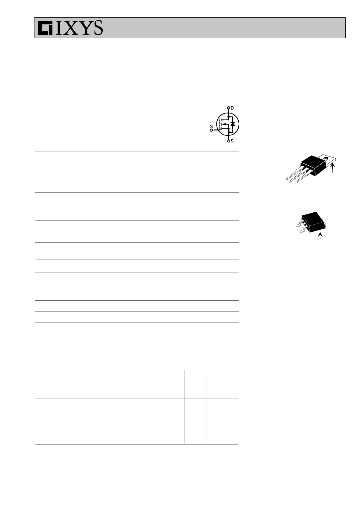
TO-220 (IXFP)
G
D
S
TO-263 (IXFA)
G
S
G = Gate D = Drain
S = Source TAB = Drain
Features
• IXYS advanced low Qg process
• Low gate charge and capacitances
- easier to drive
- faster switching
• International standard packages
• Low R
• Rated for unclamped Inductive load
DS (on)
Switching (UIS)
• Molding epoxies meet UL 94 V-0
flammability classification
Advantages
• Easy to mount
• Space savings
• High power density
D (TAB)
D (TAB)
© 2000 IXYS All rights reserved
98705 (02/04/00)IXYS reserves the right to change limits, test conditions, and dimensions.
1 - 4
Page 2
IXF A 4N100Q
IXFP 4N100Q
Symbol Test Conditions Characteristic Values
(TJ = 25°C, unless otherwise specified)
min. typ. max.
g
C
C
C
t
t
t
t
Q
Q
Q
R
R
fs
iss
oss
rss
d(on)
r
d(off)
f
g(on)
gs
gd
thJC
thCK
VDS= 20 V; ID = 0.5 • I
VGS= 0 V, VDS = 25 V, f = 1 MHz 120 pF
VGS= 10 V, VDS = 0.5 • V
RG = 4.7 W (External), 32 ns
VGS= 10 V, VDS = 0.5 • V
(TO-220) 0.25 K/W
, pulse test 1.5 2.5 S
D25
1050 pF
30 pF
17 ns
, ID = 0.5 • I
DSS
D25
15 ns
18 ns
39 nC
, ID = 0.5 • I
DSS
D25
9nC
22 nC
0.8 K/W
Source-Drain Diode Characteristic Values
(TJ = 25°C, unless otherwise specified)
Symbol Test Conditions min. typ. max.
I
S
I
SM
VGS= 0 V 4 A
Repetitive; pulse width limited by T
JM
16 A
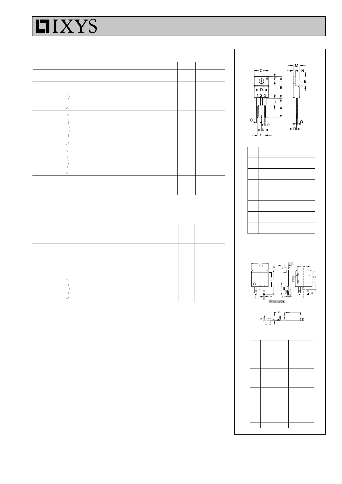
TO-220 AB (IXFP) Outline
Dim. Millimeter Inches
Min. Max. Min. Max.
A 12.70 13.97 0.500 0.550
B 14.73 16.00 0.580 0.630
C 9.91 10.66 0.390 0.420
D 3.54 4.08 0.139 0.161
E 5.85 6.85 0.230 0.270
F 2.54 3.18 0.100 0.125
G 1.15 1.65 0.045 0.065
H 2.79 5.84 0.110 0.230
J 0.64 1.01 0.025 0.040
K 2.54 BSC 0.100 BSC
M 4.32 4.82 0.170 0.190
N 1.14 1.39 0.045 0.055
Q 0.35 0.56 0.014 0.022
R 2.29 2.79 0.090 0.110
TO-263 AA (IXFA) Outline
V
SD
t
rr
Q
RM
I
RM
IF = IS, VGS = 0 V, 1.5 V
Pulse test, t £ 300 ms, duty cycle d £ 2 %
250 ns
IF = IS, -di/dt = 100 A/ms, VR = 100 V 0.52 mC
1.8 A
Dim. Millimeter Inches
Min. Max. Min. Max.
A 4.06 4.83 .160 .190
A1 2.03 2.79 .080 .110
b 0.51 0.99 .020 .039
b2 1.14 1.40 .045 .055
c 0.46 0.74 .018 .029
c2 1.14 1.40 .045 .055
D 8.64 9.65 .340 .380
D1 7.11 8.13 .280 .320
E 9.65 10.29 .380 .405
E1 6.86 8.13 .270 .320
e 2.54 BSC .100 BSC
L 14.61 15.88 .575 .625
L1 2.29 2.79 .090 .110
L2 1.02 1.40 .040 .055
L3 1.27 1.78 .050 .070
L4 0 0.38 0 .015
R 0.46 0.74 .018 .029
© 2000 IXYS All rights reserved
IXYS MOSFETS and IGBTs are covered by one or more of the following U.S. patents:
4,835,592 4,881,106 5,017,508 5,049,961 5,187,117 5,486,715
4,850,072 4,931,844 5,034,796 5,063,307 5,237,481 5,381,025
2 - 4
Page 3

IXF A 4N100Q
IXFP 4N100Q
Figure 1. Output Characteristics at 25OC Figure 2. Extended Output Characteristics at 125OC
4
TJ = 25°C
VGS = 10V
9V
8V
3
2
- Amperes
D
I
1
0
0246810
VDS - Volts
Figure 3. Output characteristics at 125°C
4
3
2
- Amperes
D
I
1
TJ = 125°C
VGS = 10V
9V
8V
6V
7V
7V
5V
6V
6
TJ = 25°C
5
VGS = 10V
9V
8V
4
3
- Amperes
D
2
I
1
0
0 4 8 12 16 20
VCE - Volts
Figure 4. Admittance Curves
4
3
TJ = 125OC
2
- Amperes
D
I
1
7V
6V
5V
TJ = 25OC
0
0 5 10 15 20
Figure 5. R
2.4
2.2
2.0
1.8
1.6
- Normalized
1.4
DS(ON)
1.2
R
1.0
0.8
0123456
normalized to 0.5 I
DS(on)
V
= 10V
GS
TJ = 125°C
ID - Amperes
VDS - Volts
TJ = 25°C
value vs. I
D25
5V
0
345678
VGS - Volts
D
Figure 6. R
normalized to 0.5 I
DS(on)
value vs. T
D25
J
2.4
2.2
VGS = 10V
ID = 2A
2.0
1.8
1.6
- Normalized
1.4
DS(ON)
1.2
R
1.0
0.8
25 50 75 100 125 150
TJ - Degrees C
© 2000 IXYS All rights reserved
3 - 4
Page 4

IXF A 4N100Q
IXFP 4N100Q
Figure 7. Gate Charge
15
V
= 600 V
12
DS
I
I
= 3 A
D
= 10 mA
G
9
- Volts
GS
6
V
3
0
0 102030405060
Gate Ch a rge - nC
Figure 9. Forward Voltage Drop of the Intrinsic Diode
10
8
Figure 8. Capacitance Curves
2000
Ciss
1000
f = 1MHz
Coss
Crss
100
Capacitance - pF
10
0 5 10 15 20 25 30 35
VDS - Volts
Figure10. Drain Current vs. Case Temperature
5
4
60
6
TJ = 125OC
4
- Amperes
D
I
TJ = 25OC
2
0
0.2 0.4 0.6 0.8 1.0 1.2
VSD - Volts
Figure 11. Transient Thermal Resistance
1.00
- K/W
0.10
JC
R(th)
3
2
- Amperes
D
I
1
0
-50 -25 0 25 50 75 100 125 150
TC - Degrees Centigrade
0.01
-4
10
© 2000 IXYS All rights reserved
10
-3
10
-2
10
-1
10
0
10
1
Pulse Width - Seconds
4 - 4
 Loading...