

Page 1
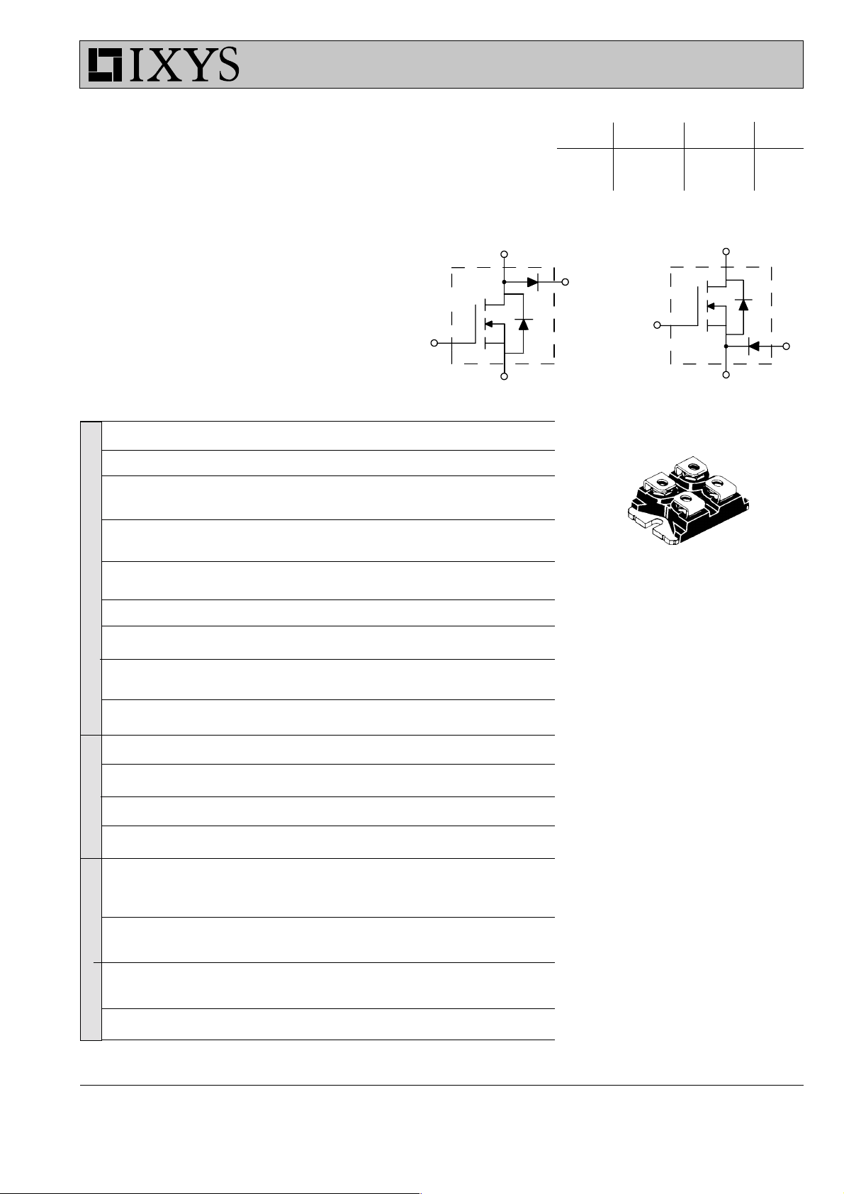
HiPerFET
TM
V
DSS
I
D (cont)
R
DS(on)
t
rr
Power MOSFETs
IXFN44N50U2 IXFN44N50U3
IXFN48N50U2 IXFN48N50U3
Buck & Boost Configurations for
3
PFC & Motor Control Circuits
Preliminary data
Symbol Test Conditions Maximum Ratings
V
DSS
V
DGR
V
GS
V
GSM
I
D25
I
DM
I
AR
E
AR
dv/dt IS £ IDM, -di/dt £ 100 A/ms, VDD £ V
P
D
V
RRM
I
FAVM
I
DIODE HiPerFET MOSFET
FRM
TJ = 25°C to 150°C 500 V
TJ = 25°C to 150°C; RGS = 1 MW 500 V
Continuous ±20 V
Transient ±30 V
TC = 25°C 44N50 44 A
48N50 48 A
TC = 25°C, 44N50 176 A
pulse width limited by max. T
48N50 192 A
JM
TC = 25°C24A
Repetitive 30 mJ
, 5 V/ns
TJ £ 150°C, RG = 2 W
DSS
TC = 25°C 520 W
TC = 70°C; rectangular, d = 0.5 60 A
tp <10 ms; pulse width limited by T
J
2
1
600 V
800 A
500 V 44 A 0.12 W 35 ns
500 V 48 A 0.10 W 35 ns
3
4
2
1
miniBLOC, SOT-227 B
1
2
4
3
Features
· Popular Buck & Boost circuit
topologies
· International standard package
miniBLOC SOT-227B
· Aluminium nitride isolation
- high power dissipation
· Isolation voltage 3000 V~
· Low R
· Rugged polysilicon gate cell structure
· Low drain-to-case capacitance
(<60 pF)
- reduced RFI
· Ultra-fast FRED diode with soft
reverse recovery
HDMOSTM process
DS (on)
4
P
D
T
J
T
JM
T
stg
V
ISOL
CASE
M
d
TC = 25°C 180 W
-40 ... +150 °C
150 °C
-40 ... +150 °C
50/60 Hz, RMS t = 1 min 2500 V~
I
£ 1 mA t = 1 s 3000 V~
ISOL
Mounting torque 1.5/13 Nm/lb.in.
Terminal connection torque (M4) 1.5/13 Nm/lb.in.
Weight 30 g
IXYS reserves the right to change limits, test conditions, and dimensions.
© 2000 IXYS All rights reserved
Applications
· Power factor controls and buck
regulators
· DC servo and robotic drives
· DC choppers
· Switch reluctance motor controls
Advantages
· Easy to mount with 2 screws
· Space savings
· Tightly coupled FRED
96535B (7/00)
1 - 5
Page 2
IXFN44N50U2 IXFN48N50U2
IXFN44N50U3 IXFN48N50U3
Symbol Test Conditions Characteristic Values
(TJ = 25°C, unless otherwise specified)
min. typ. max.
V
V
I
I
R
DSS
GS(th)
GSS
DSS
DS(on)
VGS= 0 V, ID = 1 mA 50 0 V
VDS= VGS, ID = 8 mA 2 4 V
VGS= ±20 VDC, VDS = 0 ±200 nA
VDS= 0.8 V
VGS= 0 V TJ = 125°C2mA
DSS
VGS= 10 V, ID = 0.5 I
TJ = 25°C 400 mA
44N50 0.12 W
D25
48N50 0.10 W
Pulse test, t £ 300 ms, duty cycle d £ 2 %
Symbol Test Conditions Characteristic Values
(TJ = 25°C, unless otherwise specified)
min. typ. max.
g
C
C
C
t
t
t
t
Q
Q
Q
R
R
fs
iss
oss
rss
d(on)
r
d(off)
f
g(on)
gs
gd
thJC
thCK
VDS= 10 V, ID = 0.5 I
, pulse test 22 42 S
D25
8400 pF
VGS= 0 V, VDS = 25 V, f = 1 MHz 900 pF
280 pF
30 ns
VGS= 10 V, VDS = 0.5 V
, ID = 0.5 I
DSS
D25
60 ns
RG = 1 W (External) 100 ns
30 ns
270 nC
VGS= 10 V, VDS = 0.5 V
, ID = 0.5 I
DSS
D25
60 nC
135 nC
0.24 K/W
0.05 K/W
miniBLOC, SOT-227 B
M4 screws (4x) supplied
Dim. Millimeter Inches
Min. Max. Min. Max.
A 31.50 31.88 1.240 1.255
B 7.80 8.20 0.307 0.323
C 4.09 4.29 0.161 0.169
D 4.09 4.29 0.161 0.169
E 4.09 4.29 0.161 0.169
F 14.91 15.11 0.587 0.595
G 30.12 30.30 1.186 1.193
H 38.00 38.23 1.496 1.505
J 11.68 12.22 0.460 0.481
K 8.92 9.60 0.351 0.378
L 0.76 0.84 0.030 0.033
M 12.60 12.85 0.496 0.506
N 25.15 25.42 0.990 1.001
O 1.98 2.13 0.078 0.084
P 4.95 5.97 0.195 0.235
Q 26.54 26.90 1.045 1.059
R 3.94 4.42 0.155 0.174
S 4.72 4.85 0.186 0.191
T 24.59 25.07 0.968 0.987
U -0.05 0.1 -0.002 0.004
Ultra-fast Diode Characteristic Values
(TJ = 25°C, unless otherwise specified)
Symbol Test Conditions min. typ. max.
I
R
V
TJ= 125°C; VR= 0.8V
TJ= 25°C; VR= V
R
RRM
= 0.8V
RRM
RRM
200 mA
100 mA
14 mA
VF IF = 70A, VGS = 0 V, TJ= 150°C 1.5 V
Pulse test, t £ 300 ms, duty cycle d £ 2 % T
t
rr
II = 1A, di/dt = -200 A/ms, VR = 30 V, TJ = 25°C3550ns
= 25°C 1.8 V
J
IRM IF= 60A, di/dt = -480 A/ms, VR = 350 V, TJ = 100°C 19 21 A
R
thJC
R
thJK
© 2000 IXYS All rights reserved
0.05 K/W
IXYS MOSFETS and IGBTs are covered by one or more of the following U.S. patents:
4,835,592 4,881,106 5,017,508 5,049,961 5,187,117 5,486,715
4,850,072 4,931,844 5,034,796 5,063,307 5,237,481 5,381,025
0.7 K/W
2 - 5
Page 3

IXFN44N50U2 IXFN48N50U2
IXFN44N50U3 IXFN48N50U3
Fig.1 Output Characteristics Fig.2 Input Admittance
100
90
= 25°C
T
J
VGS = 10V
7V
80
70
60
50
40
- Amperes
D
I
30
20
10
0
0 5 10 15 20 25 30 35
VDS - Volts
Fig.3 R
vs. Drain Current Fig.4 Temperature Dependence
DS(on)
1.6
T
= 25°C
J
1.5
1.4
1.3
1.2
- Norm alized
DS(on)
1.1
R
VGS = 10V
V
GS
1.0
= 15V
6V
5V
100
90
80
70
T
= 25°C
J
60
50
40
- Amperes
D
I
30
20
10
0
012345678910
VGS - Volts
of Drain to Source Resistance
2.50
2.25
2.00
1.75
1.50
- Norm alized
1.25
DS(on)
1.00
R
0.75
I
= 24A
D
0.9
0 102030405060708090100
ID - Amperes
0.50
-50 -25 0 25 50 75 100 125 150
TJ - Degrees C
Fig.5 Drain Current vs. Fig.6 Temperature Dependence of
Case Temperature Breakdown and Threshold Voltage
60
50
40
48N50
44N50
30
- Amperes
D
I
20
10
0
-50-250 255075100125150
TC - Degrees C
1.2
V
GS(th)
1.1
1.0
0.9
- Normalized
0.8
G(th)
0.7
BV/V
0.6
0.5
-50 -25 0 25 50 75 100 125 150
TJ - Degrees C
BV
DSS
© 2000 IXYS All rights reserved
3 - 5
Page 4

IXFN44N50U2 IXFN48N50U2
IXFN44N50U3 IXFN48N50U3
Fig.7 Gate Charge Characteristic Curve Fig.8 Capacitance Curves
10
VDS = 250V
9
= 24A
I
D
8
I
= 10mA
G
7
6
5
- Volts
GE
4
V
3
2
1
0
0 50 100 150 200 250 300 350 400
Gate Charge - nCoulombs
Fig.9 Source Current vs. Source
to Drain Voltage
100
90
80
70
60
50
40
- Amperes
D
I
30
20
10
0
0.00 0.25 0.50 0.75 1.00 1.25 1.50
TJ = 125°C
T
= 25°C
J
Capacitance - pF
10000
9000
8000
7000
6000
5000
f = 1 MHz
= 25V
V
DS
4000
3000
2000
1000
0
0 5 10 15 20 25
VDS - Volts
C
iss
C
oss
C
rss
VSD - Volt
Fig.10 Transient Thermal Impedance
0.1
Thermal Response - K/W
0.01
0.001 0.01 0.1 1
© 2000 IXYS All rights reserved
Time - Seconds
4 - 5
Page 5

IXFN44N50U2 IXFN48N50U2
IXFN44N50U3 IXFN48N50U3
Fig. 11. Forward voltage drop. Fig. 12. Recovery charge versus -diF/dt. Fig. 13. Peak reverse current vs. -diF/dt.
Fig. 14. Dynamic parameters versus Fig. 15. Recovery time versus -diF/dt. Fig. 16. Peak forward voltage and forward
junction temperature. recovery time vs. diF/dt.
Fig. 17. Transient thermal impedance junction to case.
© 2000 IXYS All rights reserved
5 - 5
 Loading...