

Page 1
查询IXFC52N30P供应商
Advance Technical Information
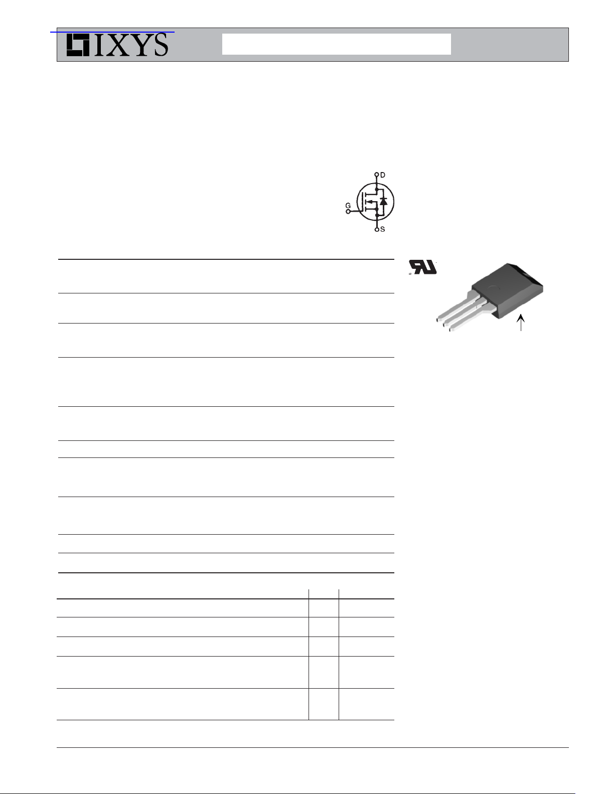
PolarHT
TM
HiPerFET
IXFC52N30P V
I
Power MOSFET
N-Channel Enhancement Mode
Symbol Test Conditions Maximum Ratings
V
DSS
V
DGR
V
GSS
V
GSM
I
D25
I
DM
I
AR
E
AR
E
AS
TJ= 25°C to 150°C 300 V
TJ= 25°C to 150°C; RGS = 1 MΩ 300 V
Continuous ±20 V
Transient ±30 V
TC= 25°C32A
TC= 25°C, pulse width limited by T
JM
150 A
TC= 25°C52A
TC= 25°C30mJ
TC= 25°C 1.0 J
DSS
D25
R
DS(on)
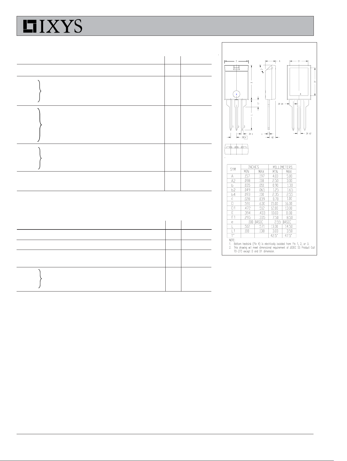
ISOPLUS220
= 300 V
= 32 A
= 75 m
TM
(IXFC)
E153432
G
D
S
G = Gate D = Drain
S = Source TAB = Drain
ΩΩ
Ω
ΩΩ
dv/dt I
≤ IDM, di/dt ≤ 100 A/µs, VDD ≤ V
S
, 10 V/ns
DSS
TJ≤ 150°C, RG = 4 Ω
P
D
T
J
T
JM
T
stg
T
L
V
ISOL
F
C
TC= 25°C 100 W
-55 ... +150 °C
150 °C
-55 ... +150 °C
1.6 mm (0.062 in.) from case for 10 s 300 ° C
50/60 Hz, RMS, t = 1minute, leads-to-tab 2500 V~
Mounting Force 11..65/2.5..15 N/lb
Weight ISOPLUS220 2.0 g
Symbol Test Conditions Characteristic Values
(TJ = 25°C, unless otherwise specified) Min. Typ. Max.
V
V
I
I
DSS
GS(th)
GSS
DSS
VGS= 0 V, ID = 250 µA 300 V
VDS= VGS, ID = 4 mA 2.5 5.0 V
VGS= ±20 VDC, VDS = 0 ±100 nA
VDS= V
DSS
25 µA
VGS= 0 V TJ = 125°C 250 µA
R
DS(on)
VGS= 10 V, ID = 0.5 I
D25
65 75 m Ω
Pulse test, t ≤ 300 µs, duty cycle d ≤ 2 %
Features
z
Silicon chip on Direct-Copper-Bond
substrate
- High power dissipation
- Isolated mounting surface
- 2500V electrical isolation
z
Low drain to tab capacitance(<30pF)
Advantages
z
Easy to mount
z
Space savings
z
High power density
© 2003 IXYS All rights reserved
DS99115A(04/05)
Page 2
IXFC 52N30P
Symbol Test Conditions Characteristic Values
(TJ = 25°C, unless otherwise specified)
Min. Typ. Max.
g
C
C
C
t
t
t
t
Q
Q
Q
R
R
fs
iss
oss
rss
d(on)
r
d(off)
f
g(on)
gs
gd
thJC
thCK
VDS= 10 V; ID = 0.5 I
VGS = 0 V, VDS = 25 V, f = 1 MHz 550 pF
VGS= 10 V, VDS = 0.5 V
RG= 4 Ω (External) 60 n s
VGS= 10 V, VDS = 0.5 V
, pulse test 20 30 S
D25
3490 pF
130 pF
24 ns
DSS
, ID = I
D25
22 ns
20 ns
110 nC
, ID = 0.5 I
DSS
D25
25 nC
53 nC
1.25 K/W
0.21 K/W
Source-Drain Diode Characteristic Values
(TJ = 25°C, unless otherwise specified)
Symbol Test Conditions min. typ. max.
ISOPLUS220 Outline
I
S
I
SM
V
SD
VGS = 0 V 32 A
Repetitive 150 A
IF = IS, VGS = 0 V, 1.5 V
Pulse test, t ≤ 300 µs, duty cycle d ≤ 2 %
T
rr
IF = 25A
250
ns
-di/dt = 100 A/µs
Q
RM
V
= 100V
R
1.0
µC
IXYS reserves the right to change limits, test conditions, and dimensions.
IXYS MOSFETs and IGBTs are covered by 4,835,592 4,931,844 5,049,961 5,237,481 6,162,665 6,404,065 B1 6,683,344 6,727,585
one or moreof the following U.S. patents: 4,850,072 5,017,508 5,063,307 5,381,025 6,259,123 B1 6,534,343 6,710,405B2 6,759,692
4,881,106 5,034,796 5,187,117 5,486,715 6,306,728 B1 6,583,505 6,710,463
Page 3

V
IXFC 52N30P
Fig. 1. Output Characteristics
@ 25 Deg. C
55
50
45
40
35
30
25
- A mperes
D
20
I
15
10
5
0
00.511.522.533.544.55
V
= 10V
GS
8V
V
- Volts
D S
7V
6V
5V
Fig. 3. Output Characteristics
@ 125 Deg. C
55
50
45
40
35
30
25
- Amperes
D
I
20
15
10
5
0
012345678910
V
= 10V
GS
8V
7V
V
- Volts
D S
6V
5V
Fig. 2. Extended Output Characteristics
@ 25 deg. C
150
125
100
75
- Amperes
D
I
50
25
0
0 5 10 15 20 25
Fig. 4. R
DS(on)
V
= 10V
GS
9V
V
- Volts
D S
Normalized to I
8V
7V
6V
5V
D25
Junction Temperature
3
2.8
2.6
2.4
2.2
1.8
1.6
- Normal ize d
1.4
D S (on)
1.2
R
0.8
0.6
0.4
VGS = 10V
2
ID = 52A
ID = 26A
1
-50 -25 0 25 50 75 100 125 150
TJ - Degrees Centigrade
alue vs.
Fig. 6. Drain Current vs. Case
Temperature
-50 -25 0 25 50 75 100 125 150
TC - Degrees Centigrade
3.8
3.4
2.6
2.2
Fig. 5. R
VGS = 10V
3
Normalized to I
DS(on)
Value vs. I
TJ = 125ºC
D
- Normal ize d
1.8
D S (on)
R
1.4
1
0.6
0 25 50 75 100 125 150
TJ = 25ºC
I D - Amperes
D25
60
50
40
30
- Amperes
D
I
20
10
0
© 2003 IXYS All rights reserved
Page 4

IXFC 52N30P
Fig. 7. Input Admittance
100
90
80
70
60
50
- Amperes
40
D
I
30
20
10
TJ = 125ºC
25ºC
-40ºC
0
44.555.566.577.58
V
- Volts
G S
Fig. 9. Source Current vs.
Source-To-Drain Voltage
150
125
100
75
- Amperes
S
I
50
25
0
0.4 0.6 0.8 1 1.2 1.4
TJ = 125ºC
V
- Volts
S D
TJ = 25ºC
Fig. 8. Transconductance
60
50
TJ = -40ºC
40
25ºC
125ºC
30
- Siemens
f s
20
g
10
0
0 102030405060708090100
I D - Amperes
Fig. 10. Gate Charge
10
V
= 150V
9
8
7
6
5
- Vol ts
G S
4
V
3
2
1
0
DS
I
= 26A
D
I
= 10m A
G
0 20 40 60 80 100 120
Q G - nanoCoulombs
Fig. 11. Capacitance
10000
f = 1MHz
C
iss
1000
C
oss
Capacitance - pF
C
rss
100
0 5 10 15 20 25 30 35 40
IXYS reserves the right to change limits, test conditions, and dimensions.
V
D S
- Volts
Fig. 12. Forw ard-Bias Safe
Operating Area
1000
TC = 25ºC
= 15 0ºC
T
R
Limit
DS
(on)
100
- Amperes
D
I
10
DC
1
10 100 1000
V
- Volts
D S
J
25µs
1ms
10ms
1 00ms
Page 5

IXFC 52N30P
Fig. 6. Drain Current vs. Case
Te mperature
27
24
21
18
15
12
- Amperes
D
I
9
6
3
0
-50 -25 0 25 50 75 100 125 150
TC - Degrees Centi grade
Fig. 13. Maximum Tr ansient The rma l Resistance
Fig. 12. Forward-Bias Safe
Operating Area
1000
TC = 25ºC
=15 0ºC
T
J
R
Limit
DS
(on)
100
25µs
- Amperes
D
I
10
DC
1
10 100 1000
V
- Vol ts
D S
1ms
10ms
1 00m s
10.00
1.00
(ºC/W)
-
(th) J C
R
0.10
0.01
0.1 1 10 100 1000
Pulse Width - milliseconds
© 2003 IXYS All rights reserved
 Loading...