

Page 1
Inverter Interface and Digital Deadtime Generator
for 3-Phase PWM Controls
Type Package Configuration Temp. Range
IXDP630 PI 18-Pin Plastic DIP RC Oscillator -40°C to +85°C
IXDP631 PI 18-Pin Plastic DIP Crystal Oscillator -40°C to +85°C
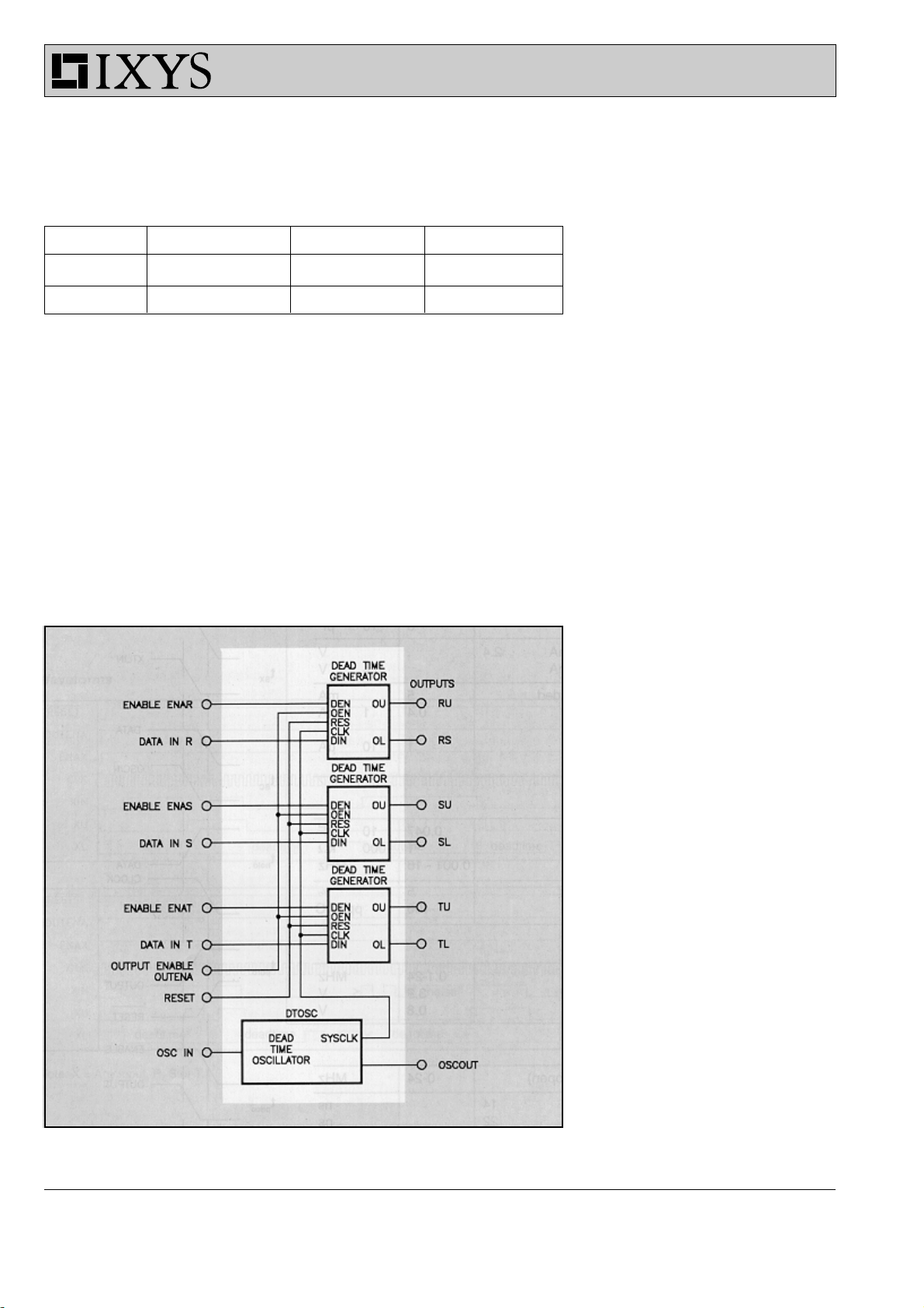
This 5 V HCMOS integrated circuit is
intended primarily for application in
three-phase, sinusoidally commutated
brushless motor, induction motor, AC
servomotor or UPS PWM modulator
control systems. It injects the required
deadtime to convert a single phase leg
PWM command into the two separate
logic signals required to drive the upper
and lower semiconductor switches in a
PWM inverter. It also provides facilities
for output disable and fast overcurrent
and fault condition shutdown.
In the IXDP630, deadtime programming
is achieved by an internal RC oscillator.
In the IXDP631, programming is
achieved by use of a crystal oscillator.
An alternative for both the IXDP630/
631 is with an external clock signal.
Because of its flexibility, the IXDP630/
631 is easily utilized in a variety of
brushed DC, trapezoidally commutated
brushless DC, hybrid and variable
reluctance step and other more exotic
PWM motor drive power and control
circuit designs.
Block Diagram IXDP 630/IXDP 631
Features
l 5 V HCMOS logic implementation
maintains low power at high speed
l Schmitt trigger inputs and CMOS
logic levels improve noise immunity
l Simultaneously injects equal dead-
time in up to three output phases
l Replaces 10-12 standard SSI/MSI
logic devices
l Allows a wide range of PWM
modulation strategies
l Directly drives high speed
optocouplers
Applications
l 1- and 3- Phase Motion Controls
l 1- and 3- Phase UPS Systems
l General Power Conversion Circuits
l Pulse Timing and Waveform
Generation
l General Purpose Delay and Filter
l General Purpose Three Channel
"One Shot"
IXYS reserves the right to change limits, test conditions and dimensions.
I - 14
© 1998 IXYS All rights reserved
Page 2
IXDP630
IXDP631
Symbol Definition Maximum Ratings
min. max.
V
CC
V
IN
I
IN
V
0
I
0
T
stg
T
L
Supply Voltage -0.5 7 V
DC Input Voltage -0.5 VCC + 0.5 V
DC Input Current -1 1 mA
DC Output Voltage 0.5 VCC + 0.5 V
DC Output Current -25 25 mA
Storage Temperature -55 150 °C
Lead Soldering (max. 10 s) 300 °C
Recommended Operating Conditions
V
T
l
f
CC
J
0
OSC
Supply Voltage 4.5 5.5 V
Operating Temperature -40 85 °C
Output Current -8 8 mA
Oscillator Frequency 0.001 16/24 MHz
Symbol Definition/Condition Characteristic Values
min. typ. max.
V
V
V
I
C
V
V
I
I
I
t+
t-
HYS
in
in
oh
ol
CC
CCQ
CCQ
Input Hi Threshold 3.6 2.7 V
Input Lo Threshold 1.6 0.8 V
Hysteresis 1.1 V
Input Leakage Current -10 10 µA
Input Capacitance 5 10 pF
Output High Voltage lo = -8 mA 2.4 V
Output Low Voltage lo = 8 mA 0.4 V
Supply Current Outputs Unloaded 5 mA
Quiescent Current Outputs 0.4 1 mA
Unloaded IXDP630
Quiescent Current Outputs 1 10 µA
Unloaded IXDP631
DP630 Oscillator Section
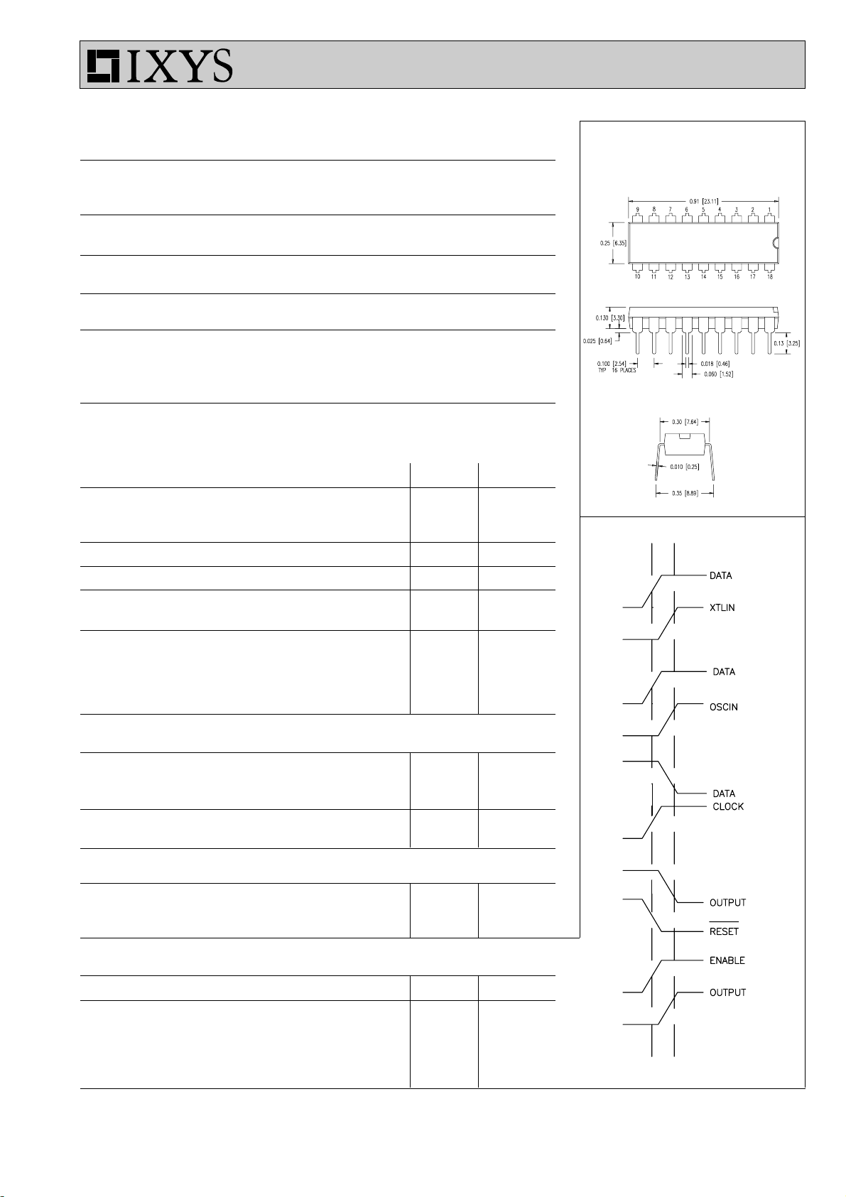
Dimensions in inch (1" = 25.4 mm)
16-Pin Plastic DIP
t
SX
t
SC
C
R
f
OSC
OSC
OSC
Capacitor (RCIN to GND) 0.047 10 nF
Resistor (OSCOUT to RCIN) 1 1000 kΩ
Frequency Range 0.001 - 16 MHz
Initial Tolerance (f
Temperature Coefficient -400 ppm/°C
DP631 Oscillator Section
f
V
V
OSC
INH
INL
Frequency Range 0.1-24 MHz
Oscillator Thresholds (IXTLIN) 3.9 V
External Oscillator
f
t
t
t
t
t
IN
SX
SC
hold
pdro
pdeo
Frequency Range (ODCOUT open) 0-24 MHz
Set Up Time DATA-to-XTLIN 14 nS
Set Up Time DATA-to-OSCIN 22 ns
Hold Time CLOCK-Data 0 ns
Propagation Delay RESET-to-OUTPUT 15 20 ns
Propagation Delay ENABLE-to-OUTPUT 8 16 ns
© 1998 IXYS All rights reserved
≤ 1MHz) 5 %
OSC
0.8 V
t
t
t
hold
pdro
pdeo
I - 15
Page 3
IXDP630
IXDP631
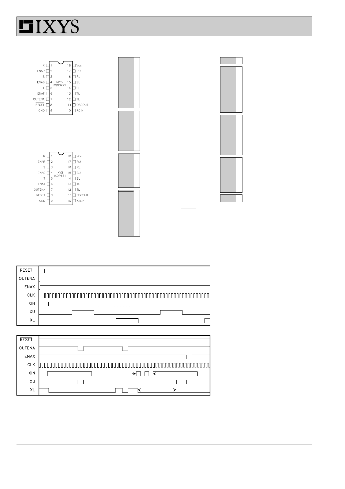
Pin Description IXDP630
Pin Description IXDP631
Sym. Pin Description
R 1 R, S and T are the three single S 3 phase inputs. Each input is
T 5 expanded into two outputs to
generate non-overlapping drive
signals, RU/RL, SU/SL, and TU/
TL. The delay from the falling
edge of one line to the rising
edge of the other is a function of
the clock.
ENAR 2 High logic input will enable the
ENAS 4 outputs, as set by the proper
ENAT 6 input phase. The ENA (R,S,T)
signals control the drive output
lines. A low logic input will force
both controlled outputs to a low
logic level
OUT 7 High logic level will enable all
ENA outputs to their related phase.
The OUTENA simultaneously
controls all outputs. Low input
logic level will inhibit all outputs
(low).
RESET 8 The RESET signal is active low.
When a logic low RESET is
applied, all outputs will go low.
After releasing the RESET
command within the generated
delay, the outputs will align with
the phase input level after the
programmed delay internal.
Sym. Pin Description
GND 9 CIRCUIT GROUND - 0 Volts
RCIN 10 The first node of the clock
or network. For the IXDP630, the
XTLIN RC input is applied to RCIN. For
OSC 11 This is the output node of the
OUT oscillator. It is connected indi-
TL 12 After the appropriate delay, the
TU 13 external drive outputs (R,S, T) U
SL 14 are in phase with their corres SU 15 ponding inputs; (R,S, T) L are
RL 16 the complementary outputs.
RU 17
V
CC
the IXDP 631, the crystal oscillator is applied to XTLIN. If an
external clock is to be supplied
to the chip it should be connected to this pin.
rectly to the RCIN or XTLIN pins
when using the internal oscillator
as described in the applications
information. It is not recommended for external use.
18 Voltage Supply +5 V ± 10 %
Waveforms
Note: X = Any input, R, S or T.
deadtime
deadtimedeadtime
deadtime deadtime
noise
deadtime
This diagram shows the normal
operation of the IXDP630/631 after the
RESET input is released. The
DEADTIME is the 8 Clock periods
between XU and XL when both XU and
XL are a "0". The length of the
DEADTIME is fixed at 8 times the
period of CLK.
The diagram shows OUTENA and ENAX
asynchronously forcing the XU Output
and the XL Output to the off state.
OUTENA will force all three channels to
the off state. ENAX (where X is one of
the three channels) will only force the
XU and XL Outputs of that channel to
the off state. Note that because ENAX
is asynchronous with respect to the
internal clock and deadtime counters,
when ENAX goes HI whatever state the
deadtime counter was in immediately
propagates to the output. This figure
also shows that noise at the XIN input
will be filtered before the XU Output or
XL Output will become active, which
may extend the deadtime.
I - 16
© 1998 IXYS All rights reserved
Page 4

IXDP630
IXDP631
Application Information
Basic Operation
The IXDP630/631 Deadtime Generators are intended to simplify the
implementation of a single- or threephase digitally controlled power
conversion circuit. It replaces one to
three digital event counters (timer/
counters) in a microcontroller or DSP
implementation of a motor control, UPS
or other power system. In most cases
these timers are at a premium. They
must be used to calculate pulse width
on one to three independent modula-
set interrupt service times, generate
tors,
a real-time clock, handle communications timing functions, etc.
The input command on the R, S and T
inputs is first synchronized with the
internal oscillator. When an input
changes state, the on output is
switched off, and after a deadtime of
exactly 8 clock periods, the complimentary output is switched on. For example, if input R is hi, output RU is hi. At
the first rising edge of CLK out after
input R is brought low, the RU output
goes low. After exactly 8 more clock
periods the RL output goes high. This
injected delay is the deadtime.
This method of synchronizing is utilized
to guarantee that the deadtime is
always exactly the same (to the accuracy of the CLK frequency). This can be
very important in certain applications.
Unbalanced deadtime creates an offset
in the PWM output stage transfer function, and can cause saturation of the
induction machine control or the driven
transformer if not corrected within a few
cycles.
Fig. 1: Totem Pole configuration of
transistor switches; reason for deadtime requirements
Deadtime in power circuits
Why is deadtime required?
Fig. 1 is typical of a switching power
conversion equipment output stage. It
has two (or typically more) switches. A
simple logic error - turning a transistor
on at the wrong instant - can cause
catastrophic failure in the right (or
wrong) circumstances.
In normal operation, when the state of
the output totem pole must change, the
conducting transistor is turned off.
Then, after a delay (usually called the
deadtime), the other transistor is turned
on. The delay is added to ensure that
there is no possibility of both transistors
conducting at the same time (this would
cause a short circuit of the DC link - a
"shoot through" - and would likely fail
both transistors in a few microseconds).
When the control logic commands a
switch to change to the off state,
several parasitics may delay/modify this
command. The propagation delay of
the control logic and gate drive buffer,
td (off) of the power transistor, storage
time (for bipolars) or tail time (for
IGBTs), voltage rise and current fall
times, etc., may be significant.
Problems Caused by Excessive
Deadtime
If a little is good, a lot should be better except with deadtime. Unfortunately,
deadband in the switching output stage
causes a nonlinearity in the power
circuit transfer function that may be
difficult for the control loop to remove.
Fig. 2 illustrates the problem. The
switching period T is:
+ t2 + DT
T = t
1
is the time Q1 is commanded on, t2 is
t
1
the time Q2 is commanded on, and DT
is the deadtime. Assuming continuous
condition, and with current in the
direction of IL1:
= t1 + DT
t
hi
tlo = t
2
With current in the direction of IL2:
= t1 + DT
t
hi
tlo = t2 + DT.
The change in "apparent duty cycle" is
then twice the deadtime (2DT). If
deadtime is 5% of the cycle period, the
duty cycle, as load current crosses
zero, instantly changes by 10 %. This is
a significant nonlinearity that causes
zero crossing distortions in load current
and voltage that must be removed by
the feedback loop around the PWM
stage. If these nonlinearities get large
enough, the loop may not have the gain
or the speed to remove them. This may
cause problems in the behavior of the
end product that are unacceptable.
Zero crossing distortion in the current of
a microstepped step motor, for example, causes very serious position errors,
velocity ripple, and audible noise in
operation - all undesirable.
I
L1
I
L2
Fig. 2: Problems caused by excessive
deadtime.
Calculating Appropriate Deadtime
Values
The designer must determine, under
worst case conditions, the absolute
maximum delay between the logic off
command and the actual cessation of
transistor conduction. This includes all
appropriate stages of logic, transistor
storage and delay times, etc. It is very
important to include special effects due
to the switch technology chosen.
Storage time of a bipolar transistor with
constant base drive can vary 10:1 as
collector current varies (storage time
increases dramatically at low collector
current, such as at light load). These
effects must be considered when
determining "worst case" delay time
requirements. A power circuit must not
only work at full rated load, but must
not fail under light or no load conditions.
A delay of at least this time (plus a
guardband) must be injected in the
command to the series transistor so as
to absolutely prohibit its turn-on during
this interval.
© 1998 IXYS All rights reserved
I - 17
Page 5

IXDP630
IXDP631
Selecting Components for a Specific
Requirement
Deadtime in the IXDP630/631 is exactly
8 clock periods: DT= 8/fclk. Once the
worst case (minimum) deadtime has
been determined (from Power switching
component manufacturer data sheets,
drive circuit analysis, breadboard
measurements, etc.) the clock
frequency is calculated: fclk(max) =
8/ DT(min).
This is the highest allowable clock
frequency, including the effects of initial
accuracy, tolerance, temperature coefficient, etc. When choosing oscillator
components, special attention to
resistor and capacitor construction is
mandatory.
Oscillator Design
There are two versions of the deadtime
generator. They have distinctly different
internal oscillator designs to serve
different application. In either case,
however, the internal oscillator can be
disabled by simply leaving its external
components off. An HCMOS compatible
clock up to 24 MHz can be fed directly
into the RCIN or XTLIN pin.
IXDP630 RC Oscillator Design
The IXDP630 uses a Schmitt trigger
inverter oscillator (Fig. 3). Two external
R
components,
the clock frequency and consequently
OSC
and C
, determine
OSC
the deadtime. This design allows a
significant cost reduction over a
standard crystal oscillator, but entails a
trade-off in frequency accuracy. The
initial accuracy and drift are a function
of the external component tolerance
and temperature coefficients, supply
voltage, and IXDP630 internal parameters. At frequencies under 1 MHz,
assuming the external components
were perfect, the IXDP630 would
introduce an initial accuracy error of
5 %, and a temperature dependence of
-400 ppm. The shift in frequency over
the VCC range 4.5 V to 5.5 V is typically
less than 5 %.
At higher frequencies and with resistor
values below 1 kΩ, the IXDP630
internal parameters become more
influential factors. This results in
greater frequency variation from one
device to another, as well as with
temperature and supply voltage
variations. If high accuracy is a
requirement, the IXDP631 with a crystal
oscillator would be the better choice.
Oscillator frequency vs. Rosc and Cosc
is shown in Fig. 4. For an analytical
method of setting the oscillator, the
design equation is for operation below
1 MHz approximately:
0.95
≈
f
OSC
Cosc Rosc
For operation above 1 MHz,
0.95
f
≈
OSC
Cosc (Rosc+30) + 3 10
-
8
IXDP631 Precision Crystal Oscillator
Design
The IXDP631 uses a more common
standard internal crystal oscillator
design. For proper operation the crystal must be of the parallel resonant
type, resonating at the crystal's fundamental frequency. Fig. 5 illustrates the
recommended oscillator configuration.
Note the external components required.
The capacitors are needed to achieve
the calibrated crystal frequency (their
value is determined by the crystal
manufacturer), and the resistor is
necessary to assure that the circuit
starts in every case. While the circuit
will usually operate without these extra
parts, this is not recommended.
The crystal oscillator in the IXDP631 is
significantly more accurate than the RC
oscillator in the IXDP630. The total
tolerance (including effects of initial
accuracy, temperature, supply voltage,
drift, etc.) is better than ±100 ppm. This
improves the accuracy and repeatability
of the desired deadtime, but at the
added expense of a crystal.
Which version is appropriate for your
application? That depends on how you
are willing to trade off component cost
for deadtime accuracy.
C
= 470 pF
OSC
C
= 270 pF
OSC
C
= 100 pF
OSC
C
= 47 pF
OSC
Fig. 3: IXDP630 internal Schmitt Trigger
inverter oscillator (R
external)
OSC
, C
OSC
are
I - 18
C
= 1 nF
OSC
C
= 2.2 nF
OSC
C
= 4.7 nF
OSC
C
= 10 nF
OSC
0.1 1 10 100 1000 10 000
Oscillator - kHz
Fig. 4. Oscillator frequency component selection for IXDP630.
© 1998 IXYS All rights reserved
Page 6

IXDP630
IXDP631
IXDP630 RC Oscillator Component
Details
The IXDP630 oscillator has only two
external components. Rosc should be
a precision, high frequency resistor.
The material used in carbon composition resistors is hydroscopic (it
absorbs water), causing resistors
above 100 kΩ to 1 MΩ to change value
with relative humidity. This is on top of
initial tolerance and temperature
coefficient deviations, and so is not
recommended. Instead, precision
metal film or carbon film resistor
construction is preferred, with initial
tolerances of 1 % and better with
temperature coefficients of ±100 ppm.
The construction of Cosc is also critical
to circuit operation. Cosc should be a
good quality monolithic ceramic (single
or multilayer) or a metallized polypropylene timing capacitor. If ceramic technology is chosen, be sure to consider
temperature coefficient and tolerance. It
is the minimum capacitor value that is
critical, not the part number rated
capacitance. A Z5U ceramic has an
initial tolerance of +80/-20 %, and a
temperature variation of +30/-80 %
over temperature. An X7R is ±10 %
initial tolerance, ±10 % over
temperature. An NPO is ±5 % initial
tolerance, ±5 % over temperature
(although tighter selections are readily
available in NPO).
If film technology is chosen, polypropylene is one of the best choices.
Tolerances down to 1 % and 2 % are
standard and temperature coefficient is
±100 ppm.
The layout of the external components
is also critical. The components should
be as close to the device as possible,
minimizing stray capacitance and
inductance.
Fig. 5. Recommended Crystal
Oscillator Components
IXDP631 Crystal Oscillator
Component Details
The IXDP631 oscillator requires three
external passive components, in
addition to the crystal. The crystal is
chosen with a frequency below fclk
(min). The capacitors and resistor
(illustrated earlier in Fig. 5) follow rules
similar to the RC oscillator option. The
resistor should be metal or carbon film,
although its accuracy and stability do
not significantly affect oscillator
frequency accuracy. The capacitors
should be monolithic ceramic
construction (CK05, or similar) with
X7R or better characteristics.
Grounding, Interfacing and Noise
Immunity
Due to the very high level of currents
that are switched at high speed in a
typical motor control power circuit,
voltage transients (V = L di/dt) can
cause serious problems. Fast digital
circuits respond to transients instead of
legitimate inputs, disturbing inverter
operation or causing outright failure.
Bypassing and Decoupling
As with any high speed logic component, the IXDP630/631 should be
bypassed with a good quality (monolithic ceramic or
film) capacitor designed
specifically for bypass application.
Decoupling is normally not required.
The IXDP630 does not generate
sufficient supply line current ripple to be
a significant noise source when
properly bypassed, and it is capable of
rejecting normal supply line noise.
Logic Levels
All inputs to the IXDP630 and IXDP631
(except XTLIN on the IXDP631) are
HCMOS Schmitt Trigger compatible.
On the IXDP631, the XTLIN pin is
different because the crystal oscillator
circuit cannot tolerate a Schmitt input.
The hysteresis inherent in Schmitt
Trigger inputs greatly improves the
reliability of digital communications. It
can reject ground bounce of up to 2 V,
and induced voltages in digital signal
traces of 1 V.
Power Circuit Noise Generation
In a typical transistor inverter, the
output MOSFET may switch on or off
with di/dt ≥ 500A/µs. Referring to Fig. 6,
and assuming that the MOSFET
Source Terminal has a 1 inch path on
the PCB to system ground, a voltage as
high as 13.5 V can be developed:
V = 27 nH
500A/µs = 13.5 V
If the MOSFET switches 25 A, the
transient will last as long as (25/500) µs
or 50 ns, which is much more than the
typical 6 or 7 ns propagation delay of a
74 HC series gate.
Caution: If one set of digital circuits is
tied to system ground, and one to local
ground, it is clear that such a transient
would cause spurious outputs. In an
inverter, the consequences of such an
error could be catastrophic. Turning a
transistor on at the wrong time could
easily cause it to explode, with the
potential for equipment damage and
operator injury -- clearly undesirable.
Fig. 6. Power circuit noise generation
Methods of Correcting these
Problems
The first step is to use a logic family
with inherent noise immunity. Standard
TTL (or any of its derivatives, including
74HCT CMOS) is a poor choice
because of the logic levels these families employ. In particular, V
close to ground to reject the levels of
OL, VIL
are too
ground noise common to power circuits.
74HC logic is significantly superior, and
the older 4000 series CMOS is even
better. Unfortunately, in modern motor
controls, especially those that employ
microprocessors, the speeds of the
4000 series CMOS are no longer
adequate. In most cases 74HC logic is
the only viable alternative.
Layout
The second, and most important step is
the printed circuit board (PCB) layout.
The PCB is a very important component in any power circuit, and there is a
© 1998 IXYS All rights reserved
I - 19
Page 7

IXDP630
IXDP631
tendency to leave it off the schematic.
During the layout process, the engineer
must consider each and every connection from the standpoint of its contribution to system operation. How sensitive
is it? What noise producing lines are
routed near it? What transients can
occur between circuits tied to each end
of this trace...? With few exceptions,
modern autorouters cannot deal with
these requirements. If autorouters are
used, they produce layouts that will not
function.
Remember that the IXDP630/631 is the
interface between the control circuits
and the power circuits. Nowhere else
on the PCB are these problems more
likely to occur. Nowhere else will one
need to pay more attention. Fig. 7
illustrates an example layout problem.
The power circuit consists of three
the MOSFET is 6 V), the di/dt at turn-on
will be regulated by the driver/MOSFET/
L
loop to about 200 A/µs - quite a
S1
surprise when your circuit requires
500 A/µs to operate correctly.
It is possible to make use of this behavior to create a turn-on or turn-off di/dt
limiter (perhaps to snub the upper
freewheeling diode reverse recovery).
While possible, this is normally not
desirable or practical where two or
more transistors are controlled.
Equalizing the parasitic impedances of
three traces while positioning the
transistors next to their heat sink and
meeting UL/VDE voltage spacings is
just too difficult.
Grounding the gate drive buffer as in
option (a) solves the MOSFET turn on
problem by eliminating LS1 from the
Fig. 7. Potential layout problems that create functional problems.
power transistors (MOSFETs in this
example) controlled by a common
digital IC (the IXDP630). With the gate
drive amplifier (a discrete circuit or
possibly an IC driver like the
IXBD4410) grounded as in option (b),
the communication path from the
IXDP630 will operate without errors.
The PC trace induced voltages are not
common with the digital path so the
input of the gate drive buffer will not
see or respond to them. Unfortunately,
the MOSFET will not operate properly.
The voltage induced across L
Q1 is turned on, acts as source dege-
when
S1
neration, modifying the turn-on behavior
of the MOSFET. If L
is 12 V (assuming the gate plateau of
= 27 nH, and V
S1
Source feedback loop. Now, unfortunately, the gate driver will oscillate every
time you turn it on or off. As the
IXDP630 output goes high, the gate
driver output follows (after its propagation delay) and the MOSFET starts to
conduct. The voltage transient induced
across LS1 (V = Ls1/di/dt) raises the
local ground (point a) until it exceeds
Voh (630)-Vil (gate buffer) and the buffer
(after its prop. delay) turns the MOSFET
off. Now the MOSFET current falls,
V(Ls1) drops, point (a) drops to (or
slightly below) system ground, and the
buffer detects a "1" at its input. After its
propagation delay, it again turns the
MOSFET on, continuing the oscillation
CC
for one more cycle.
To eliminate this problem, a ground
level transformation circuit must be
added that rejects this common mode
transient. The simplest is a decoupling
circuit, also illustrated in Fig. 7. The
capacitor voltage (on Cd) remains
constant while the transient voltage is
dropped across Rd and the buffer
detects no input transition, eliminating
the oscillation. This circuit does add
significantly to turn-on and turn-off
delay time, and cannot be used if the
transient lasts as long as these delays
are allowed to extend. Delay times
must be considered in selection of
system deadtime.
It is also important to consider the
layout of the bypass capacitor as well
as the oscillator components in order to
keep these as close to the device as
possible.
Isolation
The most complex (and most effective)
method of eliminating the effects of
transients between grounds is isolation.
Optocouplers and pulse transformers
are the most commonly used isolation
techniques, and work very well in this
case. The IXDP630/631 has been
specifically designed to directly drive a
high speed optocoupler like the Hewlett
Packard HCPL22XX family or the
General Instrument 740L60XX
optologic family. These optos are
especially well suited to motor control
and power conversion equipment due
to their very high common-mode dv/dt
rejection capabilities.
The major problem associated with
using an optocoupler in a power circuit
is its common-mode dv/dt capability.
When a lower transistor is turned on, its
Collector (or Drain) is pulled to ground
very quickly. The optocoupler that
drives the upper transistor has its local
output stage referenced to the Emitter
(Source) of this upper device, which is
tied to the Collector of the lower device.
As this node moves, the dv/dt between
here and input circuit common is impressed across the upper optocoupler.
This causes displacement currents to
flow in sensitive nodes in the optical
receiver circuitry, and may cause false
triggering of the output. Always pay
strict attention to the manufacturer's
recommended dv/dt ratings - exceeding
them could be disastrous.
I - 20
© 1998 IXYS All rights reserved
 Loading...