

Page 1

Description
end IC
for 800 MHz Cellular CDMA and 450MHz
CDMA450 mobile phones. The device has an LNA
s low
ifier and mixer have high linearity and
step gain control
ng dynamic range while saving
current. Gain, noise figure, and linearity of the
mixer can be easily adjusted using an external
The ITM1010 is fabricated on an advanced SiGe
-
nalog circuits along with
2.5mm Leadless Plastic Chip Carrier
(LPCC) package, which is the smallest CDMA
CDMA Cellular/CDMA450 Receiver RF Front-end IC
ITM1010
The ITM1010 is an integrated recei ver front-
and a down-converter on a single die. It
noise ampl
high gain. The LNA has twoscheme, increasi
inductor.
BiCMOS process which facilitates low-noise, low
power, high-frequency a
CMOS control function. The ITM1010 uses tiny 12pin 2.5mm x
Features
World ’s smallest 2.5 mm x 2.5 mm CDMA
receiver chip
Operating frequency:
CDMA Cellular : 869 ~ 894 MHz
CDMA 450 : 460 ~ 470 MHz
High linearity and high gain
Two step LNA gain control
16 dB Gain, 1.2 dB NF, 9.5 dBm IIP3 LNA
Adjustable Gain, NF, IIP3 of mixer us ing
an external inductor
All pins are ESD-protected
Tiny 12-pin LPCC package
(2.5mm × 2.5mm × 0.9mm)
Functional Block Diagram
receiver chip in the world.
Applications
Cellular CDMA/CDMA450 Mobile Phone
(@ IS-95A/B/C, CDMA2000, CDMA20001X)
450 MHz CDMA Receiver
800 MHz CDMA and TDMA Receivers
Portable Radio Handset and Equipments
Ordering Information
Part Package
ITM1010 12-pin 2.5mmx2.5mm LPCC
ITM1010TR ITM1010 Tape and Reel
ITM1010EV ITM1010 Evaluation Board (800MHz)
ITM1010EV45 ITM1010 Evaluation Board (450MHz)
For pricing, delivery, and ordering information, please contact sales@integrant.biz or visit www.integrant.biz .
02-IM1010-030827 sales@integrant.biz
Tel: 82-31-719-4500
LNAOUT
LNAOUT
9
9
10
LNAE ITM1010
10
LNAE ITM1010
LNAIN
LNAIN
11
11
Gain
Gain
Control
Control
12
12
GND
GND
LNAGAIN
LNAGAIN
MIXE
MIXE
8
8
Bias
Bias
Control
Control
ENABLE
ENABLE
MIXIN
MIXIN
7
7
321
321
LOIN
LOIN
IFP6
IFP6
IFN
5
IFN
5
VCC
4
VCC
4
Integrant Technologies Inc.
D-206, Bundang Technopark 151, Yatab-dong,
Bundang-Gu, Seongnam -Si, Kyeongki-do 463-760,
KOREA
Tel : 82-31-719-4500, Fax. : 82-31-719-4506
1/19
Page 2

ITM1010
CDMA Cellular/CDMA450 Receiver RF Front-end IC
1. Operating Conditions
1-1 Absolute Maximum Ratings
The ratings described below are stress-only, and the device’s performance might be degraded and/or
permanent damage might be caused by the stresses applied beyond these ratings.
Table 1-1 Absolute Maximum Ratings
Parameter Symbol Min Max Unit
Supply Voltage VCC -0.5 3.6 V
Digital Input Voltage to Ground VD -0.3 Vcc+0.3 V
Input Power Level P
Storage Temperature TS -40 150 °C
Junction Temperature TJ 150 °C
Lead Temperature (Soldering, 10sec) TL 240 °C
6 dBm
Imax
1-2 Recommended Operating Conditions
All device performance of ITM1010 is guaranteed under these Recommended Operating Conditions.
Table 1-2 Recommended Operation Conditions
Parameter Symbol Min Max Unit
Supply Voltage VCC 2.7 3.15 V
Operating Temperature TA -40 85 ° C
Logic High Level Input Voltage VIH 1.8 V
Logic Low Level Input Voltage VIL 0.4 V
1-3 Typical Current Consumption
Table 1-3 Typical Current Consumption
Parameter Typical Unit
Cellular CDMA
Power Down Current < 1 µA
Note: Typical current consumption is measured at 25
High Gain 28 mA
Low Gain 19 mA
°
C and Vcc=2.85V
1-4 Electrical Mode
Table 1-4 Operation Mode Control Table
ENA LNA_GAIN Operation Mode
0 X Full Power Down
1 0 LNA low gain
1 1 LNA high gain
02-IM1010-030827 sales@integrant.biz
Tel: 82-31-719-4500
2/19
Page 3

CDMA Cellular/CDMA450 Receiver RF Front-end IC
2. RF Specifications
2-1 CDMA LNA
Table 2-1 CDMA LNA RF Specifications
Specification Min Typ Max Unit Comments
RF Frequency Range 869 894 MHz
Input VSWR 2:1
Output VSWR 2:1
High Gain Mode
Gain 15 16 dB
Noise Figure 1.2 1.5 dB
Input IP3 8.5 9.5 dBm
1
ITM1010
Low Gain Mode
Gain -3.5 dB
Noise Figure 4.8 dB
Input IP3 23 dBm
2-2 CDMA Downconverter
Table 2-2 CDMA Downconverter Specifications
Specification Min Typ Max Unit Comments
RF Frequency Range 869 894 MHz
IF Frequency Range 50 85.38 300 MHz
Gain 8.5 9.5 dB
Noise Figure 9.5 10.5 dB
IIP3 8.7 10 dBm
Output Impedance 1000 Ohm
LO Power -7 dBm
1
Input VSWR 2:1
Output VSWR 2:1
LO to RF Isolation 25 dB
LO to IF Isolation 35 dB
RF to LO Isolation 26 dB
02-IM1010-030827 sales@integrant.biz
Tel: 82-31-719-4500
3/19
Page 4

CDMA Cellular/CDMA450 Receiver RF Front-end IC
2-3 CDMA Cascaded Performance
Table 2-3 CDMA Cascaded Specifications
Specification Min Typ Max Unit Comments
RF Frequency Range 869 894 MHz
IF Frequency Range 50 85.38 300 MHz
Gain 23.5 dB
Noise Figure 2.15 dB
IIP3 -4.2 dBm
IF Output Impedance 1000 Ohm
LO Level -7 dBm
Input VSWR 2:1
Output VSWR 2:1
Notes
1. The measurement condition is TA=25°C and VCC=3V with mixer emitter degeneration inductor (L4
in Fig. 4 -1) of 8.2 nH (default value).
2. Filter noise figure of 2.0dB is used for calculation of cascaded performance.
1,2
ITM1010
02-IM1010-030827 sales@integrant.biz
Tel: 82-31-719-4500
4/19
Page 5

CDMA Cellular/CDMA450 Receiver RF Front-end IC
2-4 CDMA450 LNA
Table 2-4 450MHz CDMA LNA RF Specifications
Specification Min Typ Max Unit Comments
RF Frequency Range 400 500 MHz
Input VSWR 2:1
Output VSWR 2:1
High Gain Mode
Gain 15.5 16.5 dB
Noise Figure 1.6 1.9 dB
Input IP3 8.5 9.5 dBm
Low Gain Mode
Gain -3.5 dB
3
ITM1010
Noise Figure 3.3 dB
Input IP3 25 dBm
2-5 CDMA450 Downconverter
Table 2-5 450MHz CDMA Downconverter Specifications
Specification Min Typ Max Unit Comments
RF Frequency Range 460 470 MHz
IF Frequency Range 50 85.38 300 MHz
Gain 9.5 10.5 dB
Noise Figure 8.5 10 dB
IIP3 5.7 7 dBm
Output Impedance 1000 Ohm
LO Power -10 dBm
Input VSWR 2:1
Output VSWR 2:1
3
LO to RF Isolation 25 dB
LO to IF Isolation 35 dB
RF to LO Isolation 26 dB
02-IM1010-030827 sales@integrant.biz
Tel: 82-31-719-4500
5/19
Page 6

CDMA Cellular/CDMA450 Receiver RF Front-end IC
2-6 CDMA450 Cascaded Performance
Table 2-6 450MHz CDMA Cascaded Specifications
Specification Min Typ Max Unit Comments
RF Frequency Range 460 470 MHz
IF Frequency Range 50 85.38 300 MHz
Gain 25 dB
Noise Figure 2.2 dB
IIP3 -7.6 dBm
IF Output Impedance 1000 Ohm
LO Level -10 dBm
Input VSWR 2:1
Output VSWR 2:1
Notes
3. The measurement condition is TA=25°C and VCC=2.85V with mixer emitter degeneration inductor
(L4 in Fig. 4-2) of 18 nH (default value).
4. Filter noise figure of 2.0dB is used for calculation of cascaded performance.
3,4
ITM1010
02-IM1010-030827 sales@integrant.biz
Tel: 82-31-719-4500
6/19
Page 7
CDMA Cellular/CDMA450 Receiver RF Front-end IC
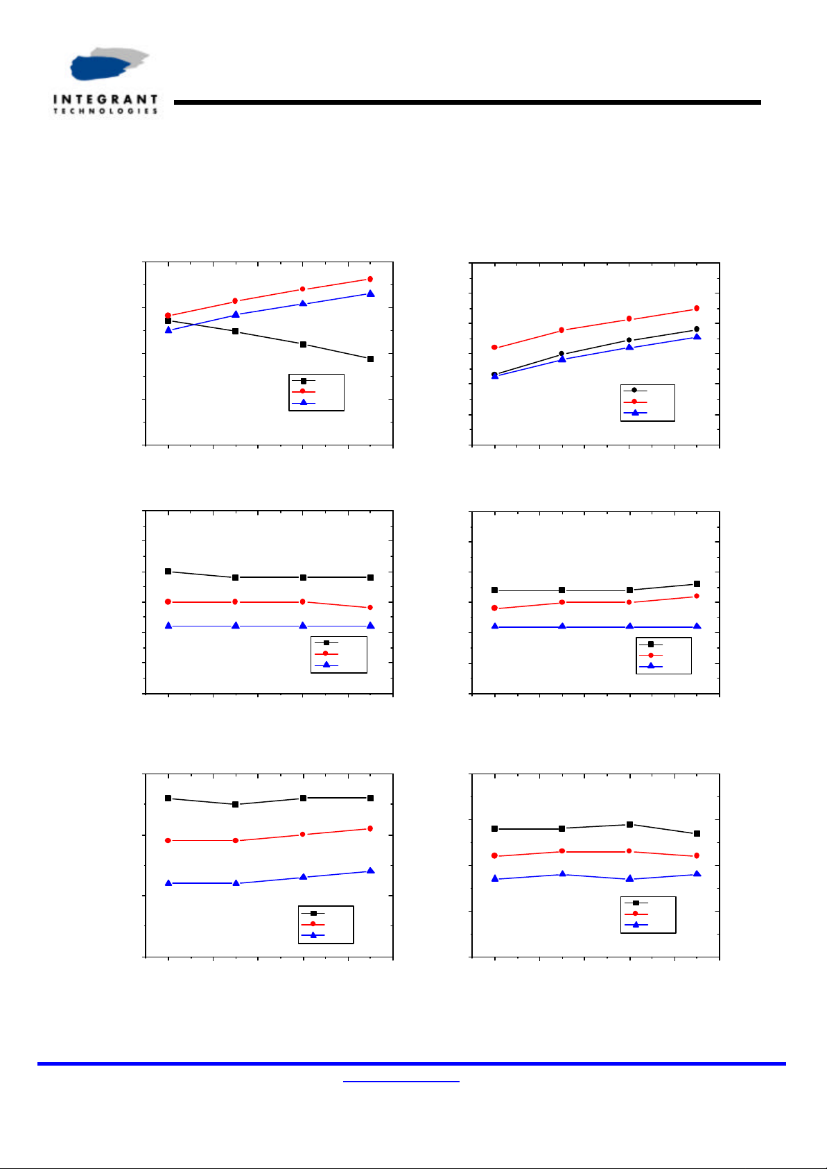
3. Typical Operating Characteristics
▶
CDMA450
ITM1010
18.0
17.5
17.0
Current (mA)
16.5
16.0
2.7 2.8 2.9 3.0 3.1 3.2
18.0
17.5
17.0
16.5
Gain (dB)
16.0
15.5
CEL LG Current vs. Vcc
-40
25
85
Vcc (V)
LNA High Gain vs. Vcc
℃
℃
℃
-40
25
85
℃
-40
℃
25
℃
85
28.0
27.5
27.0
26.5
26.0
Current (mA)
25.5
25.0
2.7 2.8 2.9 3.0 3.1 3.2
CEL HG Current vs. Vcc
Vcc (V)
-2.0
-2.5
-3.0
℃
℃
℃
-3.5
Gain (dB)
-4.0
-4.5
LNA Low Gain vs. Vcc
℃
-40
℃
25
℃
85
15.0
2.7 2.8 2.9 3.0 3.1 3.2
-5.0
Vcc (V)
10
9
8
IIP3 (dBm)
7
2.7 2.8 2.9 3.0 3.1 3.2
LNA HG-Mode IIP3 vs. Vcc
IIP3 (dBm)
℃
-40
℃
25
℃
85
Vcc (V)
02-IM1010-030827 sales@integrant.biz
Tel: 82-31-719-4500
2.7 2.8 2.9 3.0 3.1 3.2
Vcc (V)
26
25
24
23
22
2.7 2.8 2.9 3.0 3.1 3.2
LNA LG-Mode IIP3 vs. Vcc
-40
25
85
Vcc (V)
℃
℃
℃
7/19
Page 8

CDMA Cellular/CDMA450 Receiver RF Front-end IC
3. Typical Operating Characteristics(Cont’d)
▶
CDMA450
ITM1010
3.0
2.5
2.0
1.5
NF (dB)
1.0
0.5
0.0
2.7 2.8 2.9 3.0 3.1 3.2
LNA HG-Mode NF vs. Vcc
Vcc (V)
14
12
10
Mixer Gain vs. Vcc
Gain (dB)
8
-40
25 ℃
85
-40
25
85
5
4
3
℃
℃
2
NF (dB)
1
0
2.7 2.8 2.9 3.0 3.1 3.2
LNA LG-Mode NF vs. Vcc
℃
-40
℃
25
℃
85
Vcc (V)
8
6
4
℃
℃
℃
IIP3 (dBm)
Mixer IIP3 vs. Vcc
-45oC
25oC
85oC
6
2.7 2.8 2.9 3.0 3.1 3.2
Vcc (V)
10
9
8
Mixer NF vs. Vcc
NF (dB)
7
6
2.7 2.8 2.9 3.0 3.1 3.2
Gain (dB)
℃
-40
℃
25
℃
85
Vcc (V)
02-IM1010-030827 sales@integrant.biz
Tel: 82-31-719-4500
2
2.7 2.8 2.9 3.0 3.1 3.2
Vcc (V)
14
12
10
8
6
-25 -20 -15 -10 -5 0
Mixer Gain vs. LO Power
LO Power (dBm)
-40
25
85
℃
℃
℃
8/19
Page 9

CDMA Cellular/CDMA450 Receiver RF Front-end IC
3. Typical Operating Characteristics(Cont’d)
▶
CDMA450
ITM1010
8
7
6
IIP3 (dBm)
5
4
-25 -20 -15 -10 -5 0
Mixer IIP3 vs. LO Power
LO Power (dBm)
-40
25
85
12
10
℃
℃
℃
8
NF (dB)
6
4
-25 -20 -15 -10 -5 0
Mixer NF vs. LO Power
LO Power (dBm)
-40
25
85
℃
℃
℃
02-IM1010-030827 sales@integrant.biz
Tel: 82-31-719-4500
9/19
Page 10

CDMA Cellular/CDMA450 Receiver RF Front-end IC
4. PIN Assignment
Table 4-1 PIN Assignment Table
PIN Symbol Description
ITM1010
1 LNA_GAIN
2 ENA
3 LO_IN Mixer LO input
4 VCC Power supply voltage
5 IFN Negative mixer output (open collector)
6 IFP Positive mixer output (open collector)
7 MIX_IN Mixer RF input
8 MIX_E Mixer emitter degeneration
9 LNA_OUT LNA output (open collector). Requires external matching network.
10 LNA_E LNA emitter degeneration
11 LNA_IN LNA RF input. Requires external matching network.
12 GND Ground
LNA Gain Control Pin. With LNA_GAIN=HIGH, LNA operates at high-gain mode,
and with LNA_GAIN=LOW LNA operates at low-gain mode.
Enable Pin. If ENA is LOW, the device operates at full power-down mode. If ENA is
HIGH the device operates at active mode.
02-IM1010-030827 sales@integrant.biz
Tel: 82-31-719-4500
10/19
Page 11

CDMA Cellular/CDMA450 Receiver RF Front-end IC
5. Evaluation Board Schematic
5-1. CDMA Cellular Band(869 ~ 894 MHz)
SAW_FILTER
SAW_FILTER
C1
C1
2pF
2pF
L6
L6
220nH
C3
C3
R1
R1
C11
C11
12
12
R2
R2
30k
30k
220nH
C14
C14
5pF
5pF
C13
C13
5pF
5pF
L7
L7
220nH
220nH
VCC
VCC
6
6
6pF
6pF
5
5
4
4
100pF
100pF
VCC
VCC
3
3
1
1
C5
C5
4pF
4pF
L8
L8
12nH
7
7
IFP
IFP
MIX_IN
MIX_IN
IFN
IFN
VCC
VCC
LO_IN
LO_IN
3
3
12nH
C4
C4
47nF
47nF
L4
L4
8.2nH
9
9
LNA_OUT
LNA_OUT
Gain
Gain
Control
Control
LNA_GAIN
LNA_GAIN
1
1
8.2nH
8
8
ITM1010
ITM1010
2
2
MIX_E
MIX_E
Bias
Bias
Control
Control
ENA
ENA
L5
L5
6.8nH
6.8nH
C9
C9
1nF
1nF
C7
C7
8pF
8pF
J4
10nH
J4
10nH
C6
C6
2
2
47 nF
47 nF
L3
L3
C8
C8
100pF
100pF
0 ohm
0 ohm
R5
R5
10
10
11
11
12
12
LNA_E
LNA_E
LNA_IN
LNA_IN
GND
GND
ITM1010
VCC
VCC
C21
C21
1nF
1nF
C22
C22
1nF
1nF
SAW_FILTER
SAW_FILTER
VCC
VCC
IF +
IF +
IF -
IF -
L2
L2
L2
27nH
27nH
LNA_GAIN ENA
LNA_GAIN ENA
1
1
2
2
27nH
C20
C20
C20
5pF
5pF
5pF
3
3
Fig. 5-1 Evaluation Board Schematic for CDMA Cellular Application
02-IM1010-030827 sales@integrant.biz
Tel: 82-31-719-4500
11/19
Page 12

CDMA Cellular/CDMA450 Receiver RF Front-end IC
5-2. CDMA450 Band(460 ~ 470 MHz)
SAW_FILTER
SAW_FILTER
C1
C1
2pF
2pF
L6
L6
C21
C21
220nH
220nH
1nF
6
6
C3
C3
R2
R2
6pF
6pF
6.2k
6.2k
5
5
4
4
C11
C11
100pF
100pF
C14
C14
5pF
5pF
C13
C13
5pF
5pF
L7
L7
220nH
220nH
VCC
VCC
1nF
C22
C22
1nF
1nF
VCC
VCC
3
J4
3
J4
1
1
C5
C5
5pF
5pF
L8
L8
39nH
7
7
IFP
IFP
MIX_IN
MIX_IN
IFN
IFN
VCC
VCC
LO_IN
LO_IN
3
3
39nH
C4
C4
47nF
47nF
L4
L4
18nH
9
9
LNA_OUT
LNA_OUT
Gain
Gain
Control
Control
LNA_GAIN
LNA_GAIN
1
1
18nH
8
8
MIX_E
MIX_E
ITM1010
ITM1010
Control
Control
ENA
ENA
2
2
Bias
Bias
L5
L5
15nH
15nH
C9
C9
1nF
1nF
C7
C7
6pF
6pF
22nH
22nH
2
2
47 nF
47 nF
L3
L3
C6
C6
C8
C8
100pF
100pF
L9
L9
L9
3.3nH
3.3nH
3.3nH
10
10
11
11
12
12
LNA_E
LNA_E
LNA_IN
LNA_IN
GND
GND
ITM1010
VCC
VCC
SAW_FILTER
SAW_FILTER
IF +
IF +
IF -
IF -
VCC
VCC
L2
L2
82nH
82nH
LNA_GAIN
LNA_GAIN
ENA
ENA
C20
C20
C20
4pF
4pF
1
1
2
2
4pF
3
3
Fig. 5-2 Evaluation Board Schematic for CDMA450 Application
02-IM1010-030827 sales@integrant.biz
Tel: 82-31-719-4500
12/19
Page 13

ITM1010
CDMA Cellular/CDMA450 Receiver RF Front-end IC
6. External Components
6-1. CDMA cellular application
The external components below are used in the ITM1010 Evaluation Board, as shown in Fig. 5-1, for
800MHz CDMA cellular application.
Table 5-1 External Component Information for CDMA cellular application
Component Model Type Part Number Comment
C1 Murata, 2 pF 0402
C3 Murata, 6 pF 0402
C4 Murata, 47 nF 0402
C5 Murata, 4 pF 0402
C6 Murata, 47 nF 0402
C7 Murata, 8 pF 0402
C8 Murata, 100 pF 0402
C9 Murata, 1 nF 0402
C11 Murata, 100 pF 0402
C13 Murata, 5 pF 0402
C14 Murata, 5 pF 0402
C20 Murata, 100 pF 0402
C21 Murata, 1 nF 0402
C22 Murata, 1 nF 0402
L2 Toko, 27 nH 0402
L3 Toko, 10 nH 0402
L4 Toko, 6.8 nH 0402
L5 Toko, 6.8 nH 0402
L6 Coil Craft, 220 nH 0603
L7 Coil Craft, 220 nH 0603
L8 Toko, 12 nH 0402
R1
R2
R5
12 Ω
6.8 kΩ
0 Ω
0402
0402
0402
02-IM1010-030827 sales@integrant.biz
Tel: 82-31-719-4500
13/19
Page 14

ITM1010
CDMA Cellular/CDMA450 Receiver RF Front-end IC
6-2. CDMA450 application
The external components below are used in the ITM1010 Evaluation Board, as shown in Fig. 5-2, for
450MHz CDMA450 application.
Table 5-2 External Component Information for CDMA450 application
Component Model Type Part Number Comment
C1 Murata, 2 pF 0402
C3 Murata, 6 pF 0402
C4 Murata, 47 nF 0402
C5 Murata, 5 pF 0402
C6 Murata, 47 nF 0402
C7 Murata, 6 pF 0402
C8 Murata, 100 pF 0402
C9 Murata, 1 nF 0402
C11 Murata, 100 pF 0402
C13 Murata, 5 pF 0402
C14 Murata, 5 pF 0402
C20 Murata, 100 pF 0402
C21 Murata, 1 nF 0402
C22 Murata, 1 nF 0402
L2 Toko, 82 nH 0402
L3 Toko, 22 nH 0402
L4 Toko, 18 nH 0402
L5 Toko, 15 nH 0402
L6 Toko, 220 nH 0603
L7 Toko, 220 nH 0603
L8 Toko, 39 nH 0402
L9 Toko, 3.3 nH 0402
R2
6.8 kΩ
0402
02-IM1010-030827 sales@integrant.biz
Tel: 82-31-719-4500
14/19
Page 15

CDMA Cellular/CDMA450 Receiver RF Front-end IC
7. Package Information
D
D
NX L
NX L
(NE - 1)ⅹ e
(NE - 1)ⅹ e(NE - 1)ⅹ e
e
e
(ND - 1) ⅹ
(ND - 1) ⅹ
(ND - 1) ⅹ
e
e
e
INDEX AREA
INDEX AREA
( D/2 ⅹ E/2 )
( D/2 ⅹ E/2 )
2X
2X
2X
2X
D/2
D/2
E/2
E/2E/2
Caaa
Caaa Caaa
Caaa
Caaa Caaa
E
E
(DATUM A)
(DATUM A)
PIN 1 INDICATOR
PIN 1 INDICATOR
ITM1010
(DATUM B)
(DATUM B)
D2
D2
D2/2
D2/2
NX k
NX k
E2/2
E2/2
E2
E2
REF
REF
0.45
0.45
NX b
NX b
CbbbMBA
CbbbMBACbbbMBA
TOP VIEW
TOP VIEW
Cccc//
Cccc//
C0.08NX
C0.08NX
A1 A3 A
SIDE VIEW
SIDE VIEW
A1 A3 A
BOTTOM VIEW
BOTTOM VIEW
12L 2.5 ⅹ 2.5 - 0.5 PITCHPACKAGE
12L 2.5 ⅹ 2.5 - 0.5 PITCHPACKAGE
MAXNOMMINREF
MAXNOMMINREF
1.000.900.80A
1.000.900.80A
0.2750.250.225b
0.2750.250.225b
COMMON DIMENSIONSPACKAGE
2.602.502.40D
2.602.502.40D
1.401.301.20D2
1.401.301.20D2
2.602.502.40E
2.602.502.40E
1.401.301.20E2
1.401.301.20E2
0.50 BSCe
0.50 BSCe
0.450.400.35L
0.450.400.35L
12N
12N
3ND
3ND
3NE
3NE
TOLERANCES OF FORM POSITION
TOLERANCES OF FORM POSITION
aaa
aaa
bbb
bbb
ccc
ccc
1. Dimensioning and tolerancing confirm to ASME Y14 -1994
2. N is the total number of solder pads
3. All dimensions are in millimeter. Angles are in degrees.
COMMON DIMENSIONSPACKAGE
MAXNOMMINREF
MAXNOMMINREF
0.050.020A1
0.050.020A1
0.25 REFA3
0.25 REFA3
--0.20K
--0.20K
0.15
0.15
0.10
0.10
0.10
0.10
Fig. 7-1 Package Information
02-IM1010-030827 sales@integrant.biz
15/19
Tel: 82-31-719-4500
Page 16

ITM1010
CDMA Cellular/CDMA450 Receiver RF Front-end IC
8. Layout Guidelines
The guidelines listed below help the users to achieve the optimum performance of ITM1010 when
drawing their layout. These guidelines are recommended.
n Keep RF signal line s as short as possible to minimize unnecessary losses and radiation.
n For the best noise performance of LNA, keep the pad-to-pad distance in LNA input line as short
as possible. The minimum distance is recommended. Also, use high Q components in LNA
input-matching circuit.
n The 0 ohm resistor between pin 10(LNA_E) and ground is used as a degeneration inductor of the
LNA for 800MHz application. This component should not be eliminated. It can also be replaced
with chip inductors to increase IP3 of LNA at the cost of smaller gain and higher noise figure.
n At the mixer outputs (pin 5 and pin 6), keep the differential signal lines of the same length to
ensure signal balance. Symmetrical PCB layout is recommended.
n High value (47nF) chip capacitors in the evaluation board (Fig. 4-1) are used for optimum IP3
performance of ITM1010. Do not replace these capacitors with smaller value capacitors.
n For various duplexer and RF SAW filters, sensitivity and IMD performance can be optimized by
tuning R5, L4 and R2 in Fig. 4-1.
n Parasitic impedances at pins 8 (MIX_E) and 10 (LNA_E) might affect RF performance
significantly because these pins are used as degeneration. Short PCB lines are recommended for
these two pins.
n Generally, high LO power is preferable for high gain/IIP 3 and low noise figure of the mixer.
02-IM1010-030827 sales@integrant.biz
Tel: 82-31-719-4500
16/19
Page 17

CDMA Cellular/CDMA450 Receiver RF Front-end IC
9. Recommended PCB Land Pattern
A
A
B
B
PKG OUTLINE
PKG OUTLINE
2.5 X 2.5
2.5 X 2.5
e
e
E
E
PCB LAND
PCB LAND
SOLDER MASK OPENNING
SOLDER MASK OPENNING
PCB EXPOSED PAD
PCB EXPOSED PAD
ITM1010
SOLDER MASK
SOLDER MASK
b
b
L
L
D
M
M
[Unit: mm]
REF MIN NOM MAX
A 0.0635
B 0.2
D 1.20 1.30 1.40
E 1.20 1.30 1.40
b 0.225 0.25 0.275
e 0.50 BSC
L 0.45 0.5 0.55
N 12
M 0.1
1. N is the total number of solder pads.
2. The exposed pad must be connected to the ground through the via
holes and the via holes must be as many as possible.
3. A= Clearance from PCB thermal pad to solder mask opening.
4. B= Clearance from edge of PCB thermal pad to PCB land.
5. L= PCB land length.
6. b= PCB land width.
7. D,E= Ground thermal pad size
8. M= (PCB land length) – (Package solder pad length)
D
02-IM1010-030827 sales@integrant.biz
Tel: 82-31-719-4500
17/19
Page 18

CDMA Cellular/CDMA450 Receiver RF Front-end IC
10. Tape and Reel Information
ITM1010
02-IM1010-030827 sales@integrant.biz
Tel: 82-31-719-4500
18/19
Page 19

1010
YMDX
CDMA Cellular/CDMA450 Receiver RF Front-end IC
ITM1010
11. Device Marking
Note : The device marking can be subjected to change without any notice.
1010 Product Code Name
YMDX Lot Code
PIN 1 Identifier
02-IM1010-030827 sales@integrant.biz
Tel: 82-31-719-4500
19/19
 Loading...