

Page 1
TM
ITF87072DK8T
Data Sheet March 2000
6A, 20V, 0.037 Ohm, Dual P-Channel,
2.5V Specified Power MOSFET
Packaging
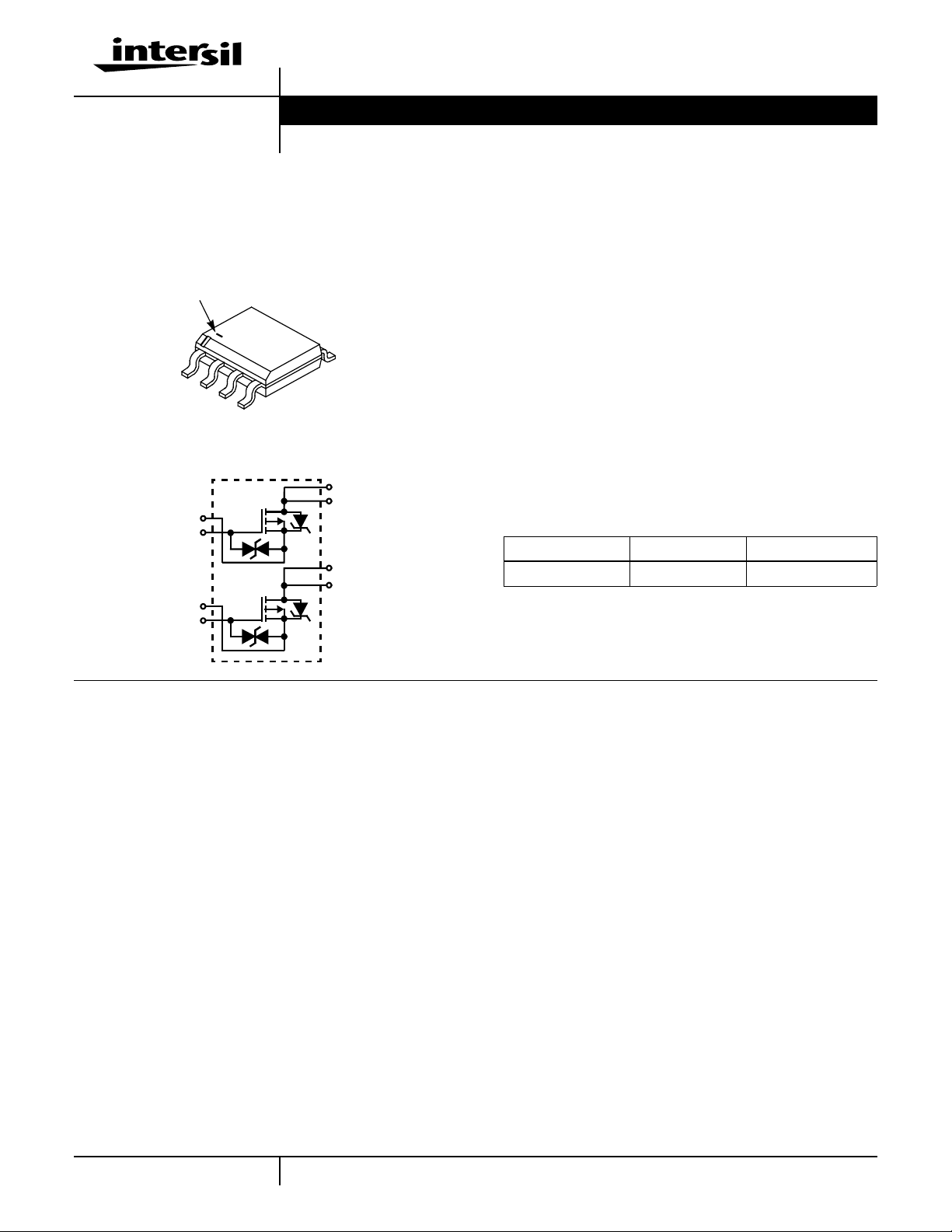
SO8 (JEDEC MS-012AA)
BRANDING DASH
5
1
2
3
4
Symbol
DRAIN1(8)
DRAIN1(7)
SOURCE1(1)
GATE1(2)
DRAIN2(6)
DRAIN2(5)
SOURCE2(3)
GATE2(4)
File Number 4812.3
Features
• Ultra Low On-Resistance
-r
-r
-r
= 0.037Ω, VGS= −4.5V
DS(ON)
= 0.039Ω, VGS= −4.0V
DS(ON)
= 0.059Ω, VGS= −2.5V
DS(ON)
• Gate to Source Protection Diode
• Simulation Models
- Temperature Compensated PSPICE™ and SABER
Electrical Models
- Spice and SABER Thermal Impedance Models
- www.intersil.com
• Peak Current vs Pulse Width Curve
• Transient Thermal Impedance Curve vs Board Mounting
Area
• Switching Time vs R
GS
Curve
Ordering Information
PART NUMBER PACKAGE BRAND
ITF87072DK8T SO8 87072
NOTE: When ordering, use the entire part number. ITF87072DK8T
is available only in tape and reel.
Absolute Maximum Ratings T
Drain to Source Voltage (Note 1). . . . . . . . . . . . . . . . . . . . . . . . . . . . . . . . . . . . . . . . . . V
Drain to Gate Voltage (RGS = 20kΩ) (Note 1) . . . . . . . . . . . . . . . . . . . . . . . . . . . . . . . .V
Gate to Source Voltage . . . . . . . . . . . . . . . . . . . . . . . . . . . . . . . . . . . . . . . . . . . . . . . . . . V
Drain Current
Continuous (TA = 25oC, VGS = -4.5V) (Note 2) . . . . . . . . . . . . . . . . . . . . . . . . . . . . . . . . I
Continuous (TA = 25oC, VGS = -4.0V) (Note 2) . . . . . . . . . . . . . . . . . . . . . . . . . . . . . . . . I
Continuous (TA = 100oC, VGS = -4.0V) (Note 3) . . . . . . . . . . . . . . . . . . . . . . . . . . . . . . . I
Continuous (TA = 100oC, VGS = -2.5V) (Note 3) . . . . . . . . . . . . . . . . . . . . . . . . . . . . . . . I
Pulsed Drain Current . . . . . . . . . . . . . . . . . . . . . . . . . . . . . . . . . . . . . . . . . . . . . . . . . . .I
Power Dissipation (Note 2) . . . . . . . . . . . . . . . . . . . . . . . . . . . . . . . . . . . . . . . . . . . . . . . . P
Derate Above 25oC . . . . . . . . . . . . . . . . . . . . . . . . . . . . . . . . . . . . . . . . . . . . . . . . . . . . . . .
Operating and Storage Temperature . . . . . . . . . . . . . . . . . . . . . . . . . . . . . . . . . . . . TJ, T
Maximum Temperature for Soldering
Leads at 0.063in (1.6mm) from Case for 10s. . . . . . . . . . . . . . . . . . . . . . . . . . . . . . . . . .T
Package Body for 10s, See Technical Brief TB370 . . . . . . . . . . . . . . . . . . . . . . . . . . .T
CAUTION: Stresses above those listed in “Absolute Maximum Ratings” may cause permanent damage to the device. This is a stress only rating and operation of the
device at these or any other conditions above those indicated in the operational sections of this specification is not implied.
NOTES:
1. TJ = 25oC to 125oC.
2. 50oC/W measured using FR-4 board with 0.14 in2 (90.3 mm2) copper pad at 1 second.
3. 228oC/W measured using FR-4 board with 0.006 in2 (3.9 mm2) copper pad at 1000 second.
= 25oC, Unless Otherwise Specified
A
DSS
DGR
GS
DM
STG
pkg
ITF87072DK8T UNITS
-20 V
-20 V
±12 V
D
D
D
D
D
L
6.0
6.0
1.5
1.5
Figure 4
2.5
20
-55 to 150
300
260
A
A
A
A
W
mW/oC
o
C
o
C
o
C
1
1-888-INTERSIL or 321-724-7143 | Intersil and Design is a trademark of Intersil Corporation. | Copyright © Intersil Corporation 2000
CAUTION: These devices are sensitive to electrostatic discharge. Follow proper ESD Handling Procedures.
SABER© is a Copyright of Analogy Inc. , PSPICE® is a registered trademark of MicroSim Corporation.
Page 2
ITF87072DK8T
Electrical Specifications T
= 25oC, Unless Otherwise Specified
A
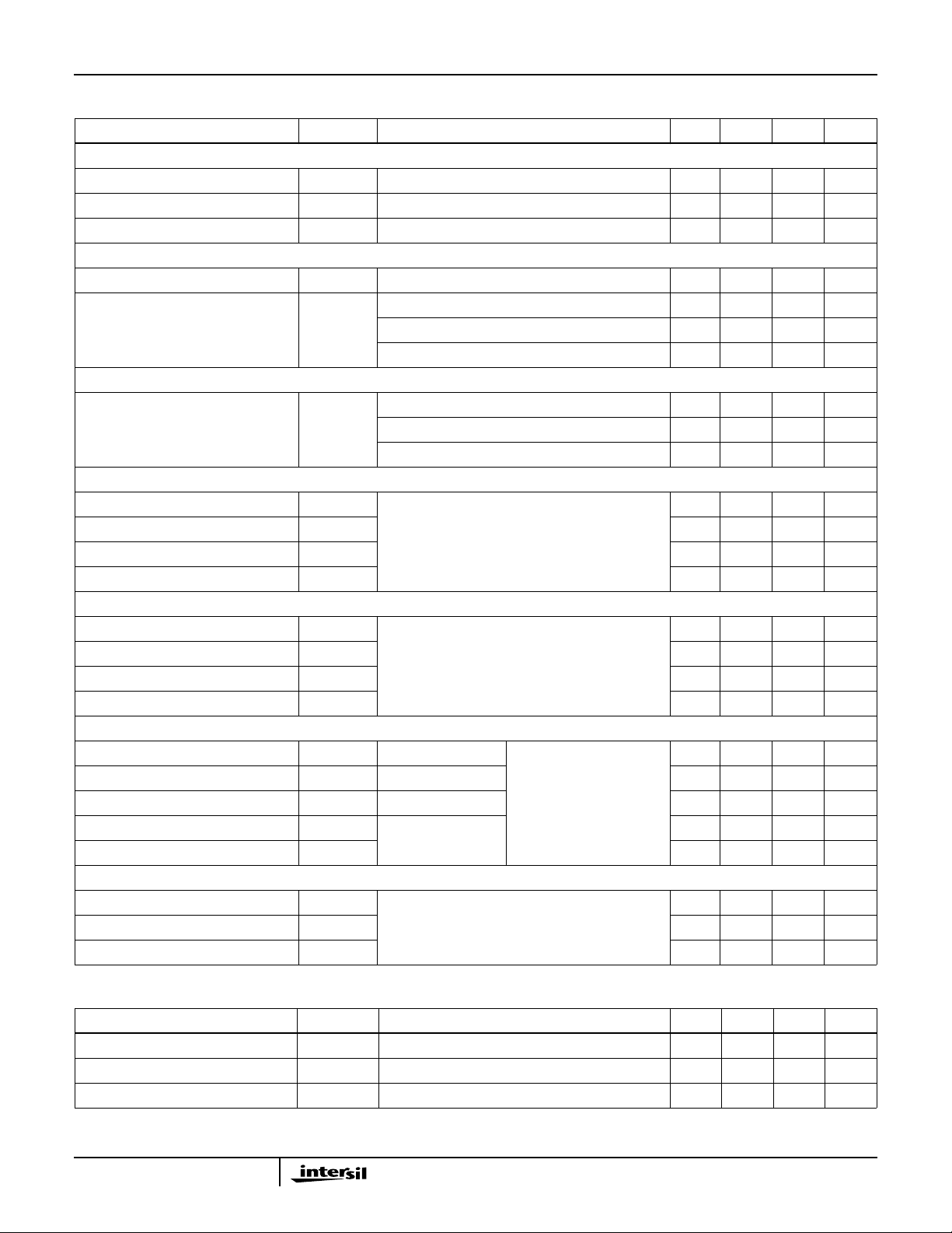
PARAMETER SYMBOL TEST CONDITIONS MIN TYP MAX UNITS
OFF STATE SPECIFICATIONS
Drain to Source Breakdown Voltage BV
Zero Gate Voltage Drain Current I
Gate to Source Leakage Current I
ON STATE SPECIFICATIONS
Gate to Source Threshold Voltage V
Drain to Source On Resistance r
THERMAL SPECIFICATIONS
Thermal Resistance Junction to
Ambient
SWITCHING SPECIFICATIONS (VGS = -2.5V)
Turn-On Delay Time t
Rise Time t
Turn-Off Delay Time t
Fall Time t
SWITCHING SPECIFICATIONS (VGS = -4.5V)
Turn-On Delay Time t
Rise Time t
Turn-Off Delay Time t
Fall Time t
GATE CHARGE SPECIFICATIONS
Total Gate Charge Q
Gate Charge at -2V Q
Threshold Gate Charge Q
Gate to Source Gate Charge Q
Gate to Drain “Miller” Charge Q
CAPACITANCE SPECIFICATIONS
Input Capacitance C
Output Capacitance C
Reverse Transfer Capacitance C
DSSID
DSS
GSS
GS(TH)VGS
DS(ON)ID
VDS = -20V, VGS = 0V - - -1 µA
VGS = ±12V - - ±10 uA
ID = 1.5A, VGS = -4.0V Figure 8 - 0.030 0.039 Ω
ID = 1.5A, VGS = -2.5V Figure 8 - 0.044 0.059 Ω
R
θJA
Pad Area = 0.14 in2(90.3 mm2) (Note 2) - - 50
Pad Area = 0.027 in2 (17.4 mm2) Figure 20 - - 191
Pad Area = 0.006 in2 (3.9 mm2) Figure 20 - - 228
d(ON)
VDD = -10V, ID = 1.5A
VGS= -2.5V,
r
RGS = 10Ω
d(OFF)
d(ON)
Figures 14, 18, 19
f
VDD = -10V, ID = 6.0A
VGS= -4.5V,
r
RGS = 10Ω
d(OFF)
g(TOT)VGS
g(-2)
g(TH)
ISS
Figures 15, 18, 19
f
VGS = 0V to -2V - 6 - nC
VGS = 0V to -0.5V - 0.7 - nC
gs
gd
VDS = -10V, VGS = 0V,
f = 1MHz
OSS
RSS
Figure 12
= 250µA, VGS = 0V Figure 11 -20 - - V
= VDS, ID = 250µA Figure 10 -0.5 - -1.5 V
= 6.0A, VGS = -4.5V Figures 8, 9 - 0.028 0.037 Ω
o
C/W
o
C/W
o
C/W
-13-ns
-85-ns
-55-ns
-62-ns
-9-ns
-72-ns
-81-ns
-82-ns
= 0V to -4.5V VDD = -10V,
-12-nC
ID = 6.0A,
I
= 1.0mA
g(REF)
Figures 13, 16, 17
- 2.5 - nC
- 3.5 - nC
- 1200 - pF
- 325 - pF
- 130 - pF
Source to Drain Diode Specifications
PARAMETER SYMBOL TEST CONDITIONS MIN TYP MAX UNITS
Source to Drain Diode Voltage V
Reverse Recovery Time t
Reverse Recovered Charge Q
2
SD
rr
RR
ISD = -6.0A - -0.85 - V
ISD = -6.0A, dISD/dt = 100A/µs - 24 - ns
ISD = -6.0A, dISD/dt = 100A/µs - 17 - nC
Page 3
Typical Performance Curves
ITF87072DK8T
1.2
1.0
0.8
0.6
0.4
0.2
POWER DISSIPATION MULTIPLIER
0
0 25 50 75 100 150
125
TA, AMBIENT TEMPERATURE (oC)
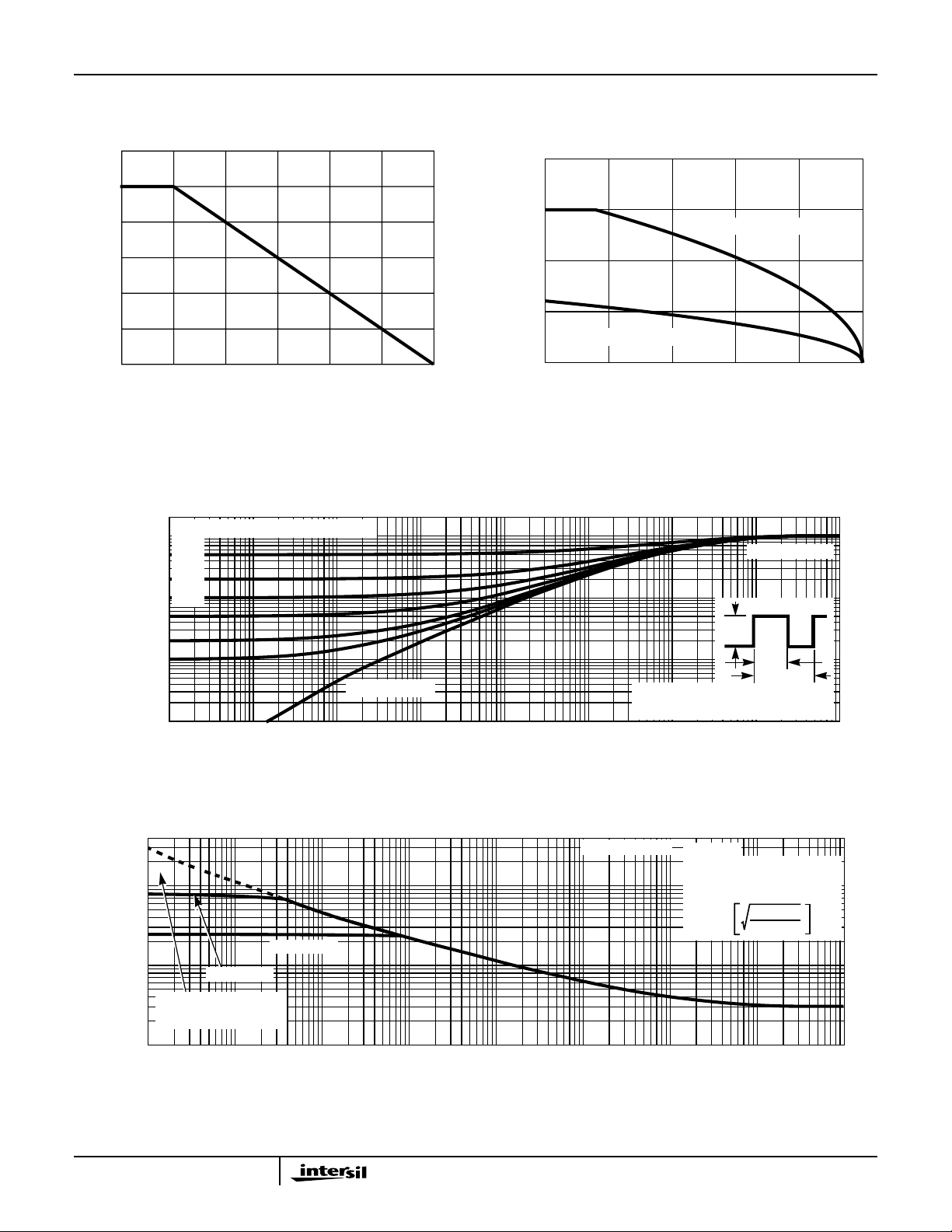
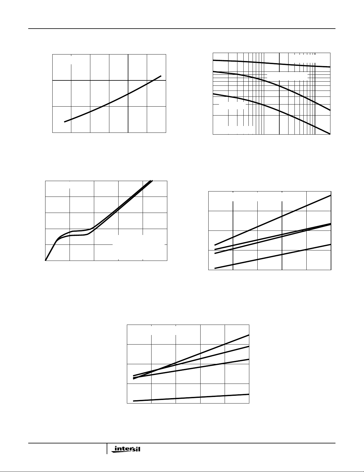
FIGURE 1. NORMALIZED POWERDISSIPATION vs AMBIENT
TEMPERATURE
2
DUTY CYCLE - DESCENDING ORDER
1
0.5
0.2
0.1
0.05
0.02
0.1
0.01
-8
-6
VGS= -4.5V, R
θJA
= 50oC/W
-4
, DRAIN CURRENT (A)
-2
D
I
VGS= -2.5V, R
0
25 50 75 100 125 150
= 228oC/W
θJA
TA, AMBIENT TEMPERATURE (oC)
FIGURE 2. MAXIMUM CONTINUOUS DRAIN CURRENT vs
AMBIENT TEMPERATURE
R
= 228oC/W
θJA
, NORMALIZED
0.01
θJA
Z
THERMAL IMPEDANCE
0.001
-5
10
-400
-100
-10
, PEAK CURRENT (A)
DM
I
TRANSCONDUCTANCE
MAY LIMIT CURRENT
IN THIS REGION
-1
-5
10
-4
10
VGS = -4.5V
-4
10
SINGLE PULSE
3
10
-2
10
-1
10
10
NOTES:
DUTY FACTOR: D = t
PEAK TJ = PDM x Z
0
1
10
t, RECTANGULAR PULSE DURATION (s)
FIGURE 3. NORMALIZED MAXIMUM TRANSIENT THERMAL IMPEDANCE
R
= 228oC/W
θJA
VGS = -2.5V
-3
10
-2
10
-1
10
t, PULSE WIDTH (s)
0
10
1
10
P
DM
t
1
t
2
1/t2
x R
θJA
+ T
θJA
A
2
10
TC = 25oC
FOR TEMPERATURES
ABOVE 25oC DERATE PEAK
CURRENT AS FOLLOWS:
150 - T
I = I
25
A
125
2
10
3
10
3
10
FIGURE 4. PEAK CURRENT CAPABILITY
3
Page 4
Typical Performance Curves (Continued)
ITF87072DK8T
-200
-100
-10
, DRAIN CURRENT (A)
OPERATION IN THIS
D
I
AREA MAY BE
LIMITED BY r
-1
-1 -10
DS(ON)
, DRAIN TO SOURCE VOLTAGE (V)
V
DS
SINGLE PULSE
TJ = MAX RATED
T
= 25oC
A
R
= 228oC/W
θJA
100µs
1ms
10ms
-50
-25
PULSE DURATION = 80µs
DUTY CYCLE = 0.5% MAX
= 15V
V
DD
-20
-15
-10
DRAIN CURRENT (A)
D,
I
-5
TJ = 25oC
-0
-1.0 -1.5 -2.0 -2.5 -3.0
TJ = 150oC
TJ = -55oC
VGS, GATE TO SOURCE VOLTAGE (V)
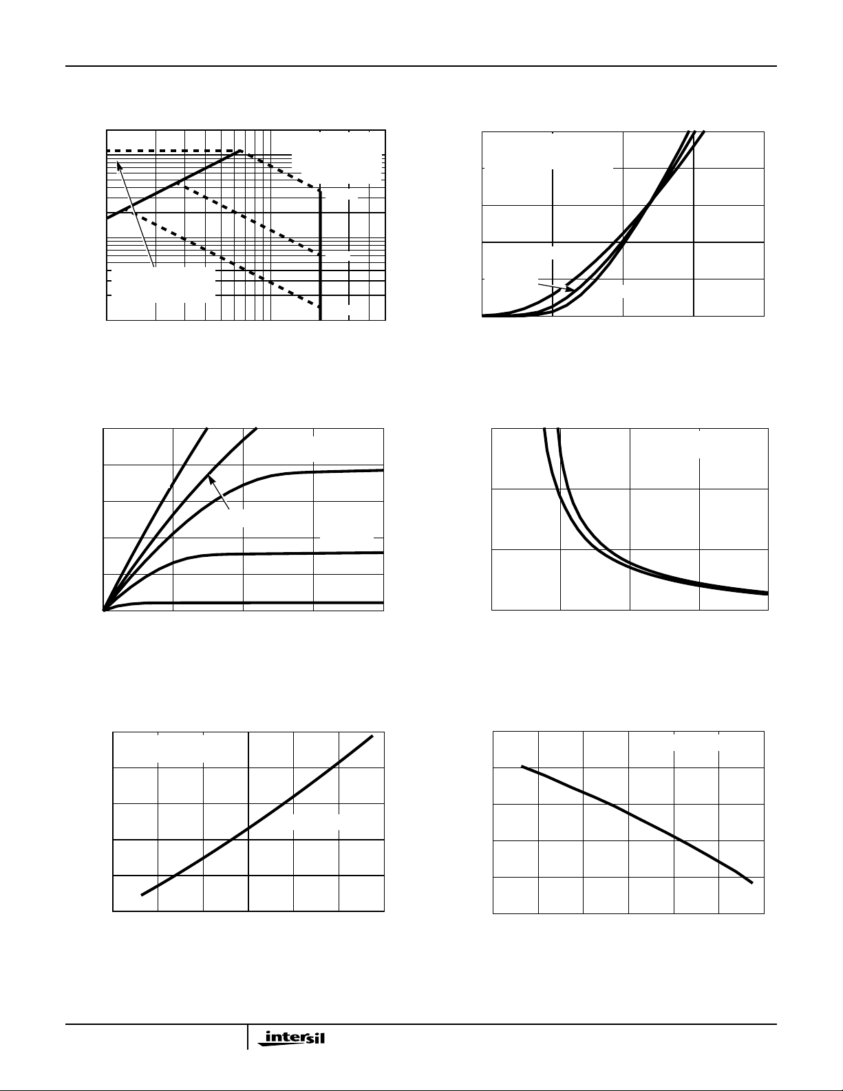
FIGURE 5. FORWARD BIAS SAFE OPERATING AREA FIGURE 6. TRANSFER CHARACTERISTICS
-25
TA = 25oC
-20
VGS = -4.5V
-15
-10
, DRAIN CURRENT (A)
D
I
-5
0
0 -0.5 -1.0 -1.5 -2.0
VDS, DRAIN TO SOURCE VOLTAGE (V)
PULSE DURATION = 80µs
DUTY CYCLE = 0.5% MAX
VGS = -3V
V
GS
VGS = -2V
VGS = -1.5V
= -2.5V
80
ID = -1.5A
60
ID = -6A
, DRAIN TO SOURCE
40
ON RESISTANCE (mΩ)
DS(ON)
r
20
-1 -2 -3 -4 -5
, GATE TO SOURCE VOLTAGE (V)
V
GS
PULSE DURATION = 80µs
DUTY CYCLE = 0.5% MAX
FIGURE 7. SATURATION CHARACTERISTICS FIGURE 8. DRAIN TO SOURCE ON RESISTANCE vs GATE
VOLTAGE AND DRAIN CURRENT
1.6
PULSE DURATION = 80µs
DUTY CYCLE = 0.5% MAX
1.4
1.2
VGS = -4.5V, ID = -6A
1.0
ON RESISTANCE
0.8
NORMALIZED DRAIN TO SOURCE
0.6
-80 -40 0 40 80 120 160
TJ, JUNCTION TEMPERATURE (oC)
FIGURE 9. NORMALIZED DRAIN TO SOURCE ON
RESISTANCE vs JUNCTION TEMPERATURE
1.4
1.2
1.0
0.8
NORMALIZED GATE
THRESHOLD VOLTAGE
0.6
0.4
-80 -40 0 40 80 120 160
TJ, JUNCTION TEMPERATURE (oC)
VGS = VDS, ID = -250µA
FIGURE 10. NORMALIZED GATE THRESHOLD VOLTAGE vs
JUNCTION TEMPERATURE
4
Page 5
Typical Performance Curves (Continued)
ITF87072DK8T
1.2
ID = -250µA
1.1
1.0
BREAKDOWN VOLTAGE
NORMALIZED DRAIN TO SOURCE
0.9
-80 -40 0 40 80 120 160
T
, JUNCTION TEMPERATURE (oC)
J
FIGURE 11. NORMALIZED DRAIN TO SOURCE BREAKDOWN
VOLTAGE vs JUNCTION TEMPERATURE
-5
VDD = -10V
-4
-3
2000
1000
C
= C
RSS
GD
C, CAPACITANCE (pF)
VGS= 0V, f = 1MHz
100
-0.1 -1 -10
VDS, DRAIN TO SOURCE VOLTAGE (V)
C
OSS
C
ISS
≅ CDS+ C
= CGS + C
GD
GD
-20
FIGURE 12. CAPACITANCE vs DRAIN TO SOURCE VOLTAGE
200
VGS = -2.5V, VDD = -10V, ID = -1.5A
t
r
150
-2
-1
, GATE TO SOURCE VOLTAGE (V)
GS
V
0
0 3 6 9 12 15
, GATE CHARGE (nC)
Q
g
WAVEFORMS IN
DESCENDING ORDER:
ID = -6A
I
= -1.5A
D
NOTE: Refer to Intersil Application Notes AN7254 and AN7260.
FIGURE 13. GATECHARGE WAVEFORMS FOR CONSTANT
GATE CURRENT
200
VGS = -4.5V, VDD = -10V, ID = -6A
150
100
50
SWITCHING TIME (ns)
100
50
SWITCHING TIME (ns)
0
0 1020304050
RGS, GATE TO SOURCE RESISTANCE (Ω)
t
f
t
d(OFF)
t
d(ON)
FIGURE 14. SWITCHING TIME vs GATE RESISTANCE
t
d(OFF)
t
f
t
r
t
d(ON)
0
0 1020304050
RGS, GATE TO SOURCE RESISTANCE (Ω)
FIGURE 15. SWITCHING TIME vs GATE RESISTANCE
5
Page 6
Test Circuits and Waveforms
ITF87072DK8T
Q
V
DS
R
L
0
gs
Q
g(TH)
Q
gd
VGS= -0.5V
VGS= -2V
g(TOT)
I
g(REF)
V
GS
V
DD
+
DUT
-V
GS
Q
g(-2)
V
DD
Q
0
I
g(REF)
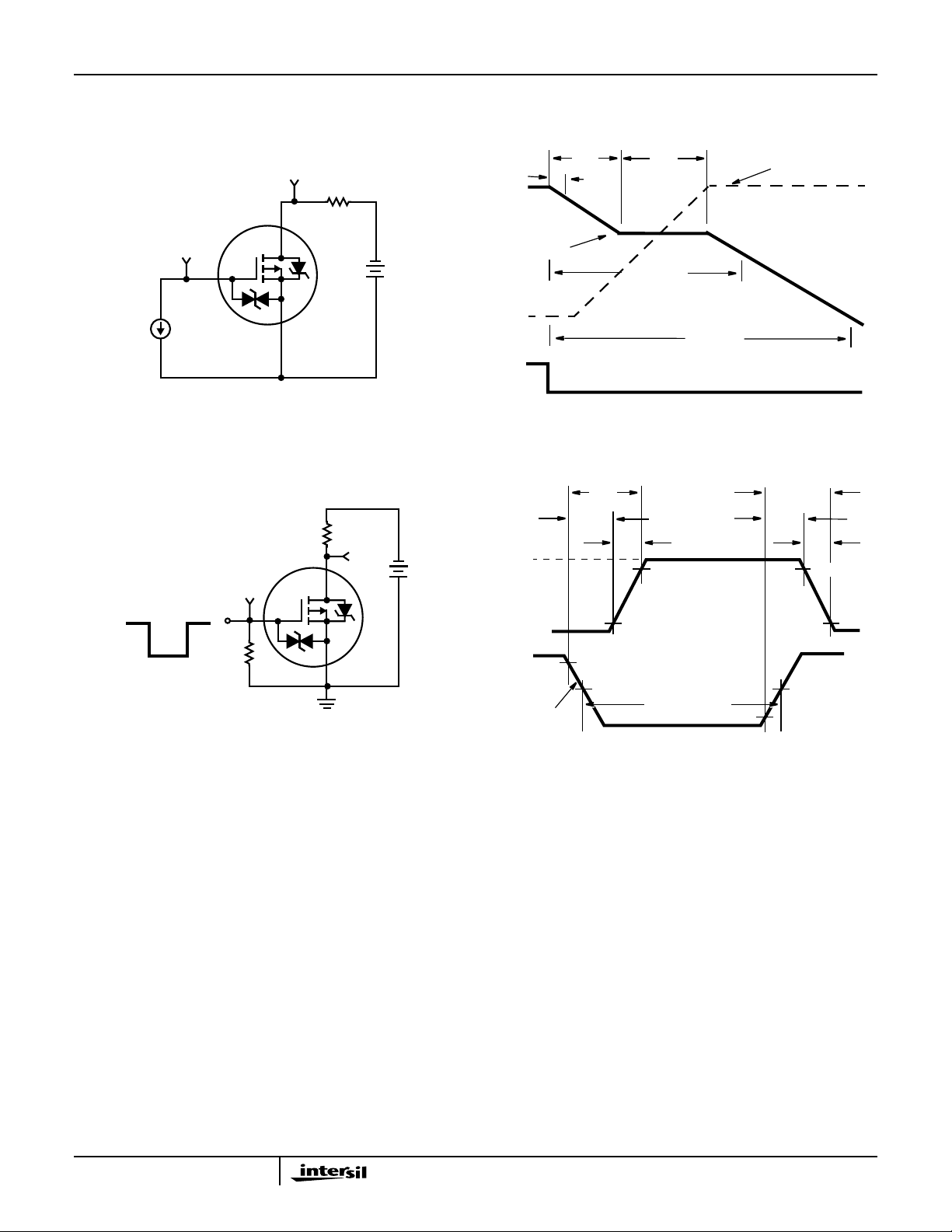
FIGURE 16. GATE CHARGE TEST CIRCUIT FIGURE 17. GATE CHARGE WAVEFORMS
t
ON
t
R
L
V
DS
V
GS
-
+
0
d(ON)
t
r
10%
V
t
d(OFF)
DS
t
OFF
VGS= -4.5V
t
f
10%
0V
DS
R
GS
-V
GS
DUT
0
V
GS
90%
10%
50%
PULSE WIDTH
V
FIGURE 18. SWITCHING TIME TEST CIRCUIT FIGURE 19. SWITCHING TIME WAVEFORM
90%
50%
90%
6
Page 7
ITF87072DK8T
Thermal Resistance vs Mounting Pad Area
Themaximum rated junction temperature, TJM, and the
thermal resistance of the heat dissipating path determines
the maximum allowabledevice powerdissipation, P
application.Therefore the application’sambient temperature,
T
(oC), and thermal resistance R
A
reviewed to ensure that T
JM
is never exceeded. Equation 1
(oC/W) must be
θJA
mathematically represents the relationship and serves as
the basis for establishing the rating of the part.
TJMTA–()
------------------------------ -=
P
DM
R
θJA
In using surface mount devices such as the SO8 package,
the environment in which it is applied will have a significant
influence on the part’s current and maximum power
dissipation ratings. Precise determination of P
DM
and influenced by many factors:
1. Mounting pad area onto whichthe deviceis attached and
whether there is copper on one side or both sides of the
board.
2. The number of copper layers and the thickness of the
board.
3. The use of external heat sinks.
4. The use of thermal vias.
5. Air flow and board orientation.
6. For non steady state applications, the pulse width, the
duty cycle and the transient thermal response of thepart,
the board and the environment they are in.
Intersil provides thermal information to assist the designer’s
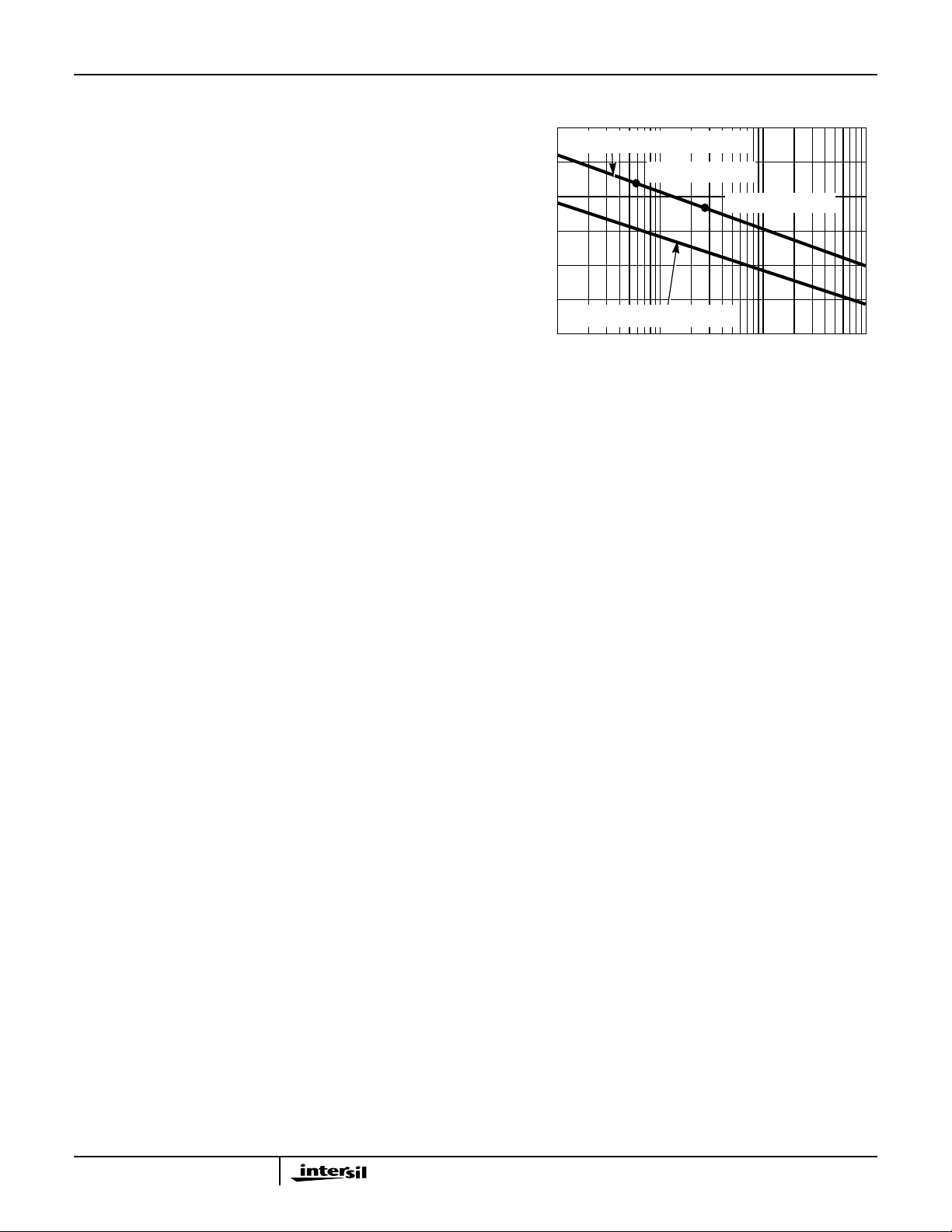
preliminary application evaluation. Figure 20 defines the
for the device as a function of the top copper
R
θJA
(component side) area. This is for a horizontally positioned
FR-4 board with 1oz copper after 1000 seconds of steady
state power with no air flow. This graph provides the
necessary information for calculation of the steady state
junction temperature or power dissipation. Pulse
applications can be evaluated using the Intersil device Spice
thermal model or manually utilizing the normalized maximum
transient thermal impedance curve.
Displayed on the curve are R
values listed in the
θJA
Electrical Specifications table. The points were chosen to
depict the compromise between the copper board area, the
thermal resistance and ultimately the power dissipation,
P
.
DM
Thermal resistances corresponding to other copper areas
can be obtained from Figure 20 or by calculation using
Equation 2. R
is defined as the natural log of the area
θJA
times a coefficient added to a constant. The area, in square
inches is the top copper area including the gate and source
pads.
R
103.2 24.3 Area()
θJA
ln×–=
,inan
DM
(EQ. 1)
is complex
(EQ. 2)
300
250
200
C/W)
o
(
θJA
150
, R
θβ
100
R
50
FIGURE 20. THERMAL RESISTANCE vs MOUNTING PAD
R
= 103.2 - 24.3 *ln(AREA)
θJA
228oC/W - 0.006in
R
= 46.4 - 21.7 *ln(AREA)
θβ
0
0.001 0.01 0.1 1
AREA, TOP COPPER AREA (in2) PER DIE
AREA
2
191oC/W - 0.027in
2
While Equation 2 describes the thermal resistance of a
single die, several devices are offered with two die in the
SO8 package. The dual die SO8 package introduces an
additional thermal component, thermal coupling resistance,
R
. Equation 3 describes Rθβ as a function of the top
θβ
copper mounting pad area.
R
θβ
46.4 21.7 Area()ln×–=
(EQ. 3)
The thermal coupling resistance vs copper area is also
graphically depicted in Figure 20. It is important to note the
thermal resistance (R
(
R
) are equivalent for both die. For example at 0.1 square
θβ
) and thermal coupling resistance
θJA
inches of copper:
R
= R
θJA1
R
= R
θβ1
and TJ2 define the junction temperature of the
T
J1
respective die. Similarly, P
= 159oC/W
θJA2
= 97oC/W
θβ2
and P2 define the power
1
dissipated in each die. The steady state junction
temperature can be calculated using Equation 4 for die 1
and Equation 5 for die 2.
Example: To calculate the junction temperature of each die
when die 2 is dissipating 0.5 Watts and die 1 is dissipating 0
Watts.The ambient temperature is 70
o
C and the package is
mounted to a top copper area of 0.1 square inches per die.
Use Equation 4 to calculate T
T
.
J2
.
T
J1P1RθJAP2
R
++=
θβ
and Equation 5 to calculate
J1
T
A
(EQ. 4)
TJ1 = (0 Watts)(159˚C/W) + (0.5 Watts)(97˚C/W) + 70˚C
= 119˚C
T
J1
T
J2P2RθJAP1
T
= (0.5 Watts)(159˚C/W) + (0 Watts)(97˚C/W) + 70˚C
J2
R
θβ
T
A
(EQ. 5)
++=
TJ2 = 150˚C
7
Page 8
ITF87072DK8T
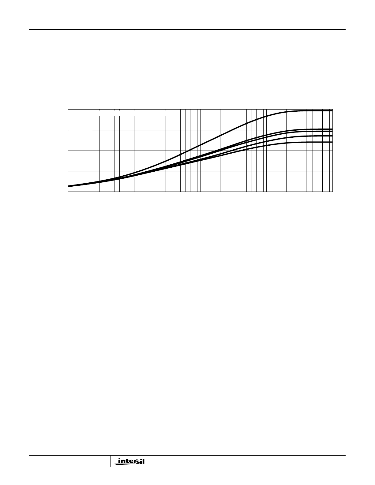
The transient thermal impedance (Z
) is also affected by
θJA
varied top copper board area. Figure 21 shows the effect of
copper pad area on single pulse transient thermal
impedance. Each trace represents a copper pad area in
square inches corresponding to the descending list in the
graph. Spice and SABER thermal models are provided for
each of the listed pad areas.
160
COPPER BOARD AREA - DESCENDING ORDER
2
0.020 in
2
0.140 in
2
0.257 in
120
C/W)
o
80
, THERMAL
JA
θ
Z
IMPEDANCE (
40
0
10
0.380 in
0.493 in
-1
2
2
0
10
t, RECTANGULAR PULSE DURATION (s)
FIGURE 21. THERMAL RESISTANCE vs MOUNTING PAD AREA
Copper pad area has no perceivable eff ect on tr ansient
thermal impedance for pulse widths less than 100ms. For
pulse widths less than 100ms the transient thermal
impedance is determined by the die and package. Therefore ,
CTHERM1 through CTHERM5 and RTHERM1 through
RTHERM5 remain constant for each of the thermal models. A
listing of the model component values is available in Table 1.
1
10
2
10
3
10
8
Page 9
ITF87072DK8T
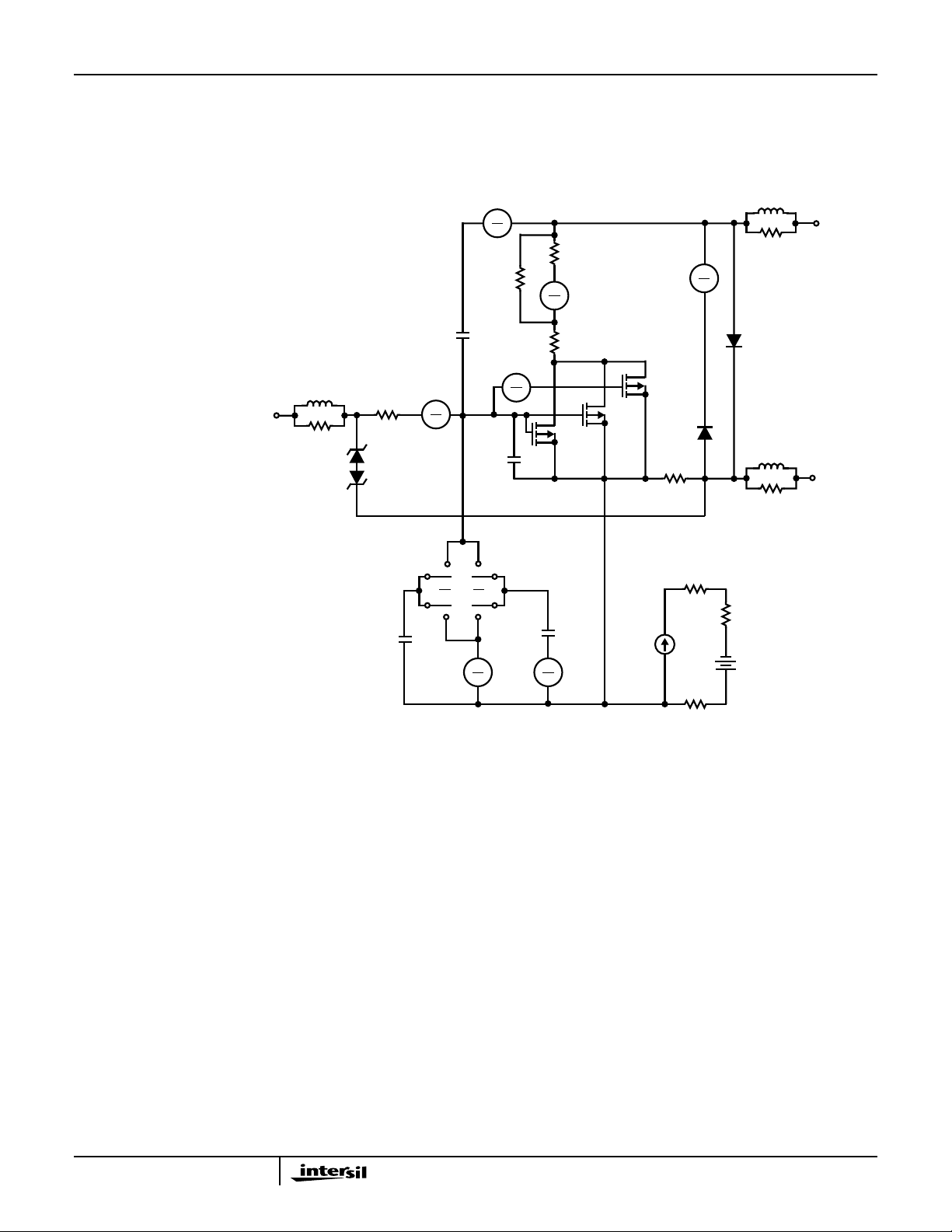
PSPICE Electrical Model
.SUBCKT ITF87072DK8 2 1 3 ; REV Dec 1999
CA 12 8 1.15e-9
CB 15 14 1.2e-9
CIN 6 8 1.09e-9
+
-
11
7
LDRAIN
RLDRAIN
DBODY
LSOURCE
RLSOURCE
RVTEMP
19
-
VBAT
+
22
DBODY 5 7 DBODYMOD
DBREAK 7 11 DBREAKMOD
DESD1 91 9 DESD1MOD
DESD2 91 7 DESD2MOD
DPLCAP 10 6 DPLCAPMOD
EBREAK 5 11 17 18 -29.6
EDS 14 8 5 8 1
EGS 13 8 6 8 1
ESG 5 10 8 6 1
EVTHRES 6 21 19 8 1
EVTEMP 6 20 18 22 1
IT 8 17 1
LDRAIN 2 5 1.0e-9
LGATE 1 9 3.6e-9
LSOURCE 3 7 4.3e-9
MMED 16 6 8 8 MMEDMOD
GATE
1
LGATE
RLGATE
RGATE
9
DESD1
91
DESD2
DPLCAP
EVTEMP
-
18
22
20
ESG
10
8
6
RSLC2
EVTHRES
+
6
+
5
+-
RSLC1
51
+
5
ESLC
51
-
50
RDRAIN
16
21
-
19
8
MSTRO
CIN
8
EBREAK
MWEAK
MMED
DBREAK
RSOURCE
17
18
MSTRO 16 6 8 8 MSTROMOD
MWEAK 16 21 8 8 MWEAKMOD
RBREAK 17 18 RBREAKMOD 1
RDRAIN 50 16 RDRAINMOD 5.8e-3
RGATE 9 20 16.1
RLDRAIN 2 5 10
RLGATE 1 9 36
RLSOURCE 3 7 43
RSLC1 5 51 RSLCMOD 1e-6
RSLC2 5 50 1e3
RSOURCE 8 7 RSOURCEMOD 1.1e-2
RVTHRES 22 8 RVTHRESMOD 1
RVTEMP 18 19 RVTEMPMOD 1
S1A 6 12 13 8 S1AMOD
S1B 13 12 13 8 S1BMOD
S2A 6 15 14 13 S2AMOD
CA
S1A
12
13
8
S1B
EGS EDS
S2A
6
8
S2B
15
CB
14
+
5
8
-
14
13
13
+
+
-
-
RBREAK
17 18
IT
8
RVTHRES
S2B 13 15 14 13 S2BMOD
VBAT 22 19 DC 1
ESLC 51 50 VALUE={(V(5,51)/ABS(V(5,51)))*(PWR(V(5,51)/(1e-6*100),2.1))}
.MODEL DBODYMOD D (IS = 1.7e-10 IKF = 3 N = 1.18 RS = 1.05e-2 TRS1 = 1.75e-3 TRS2 = 5.08e-6 CJO = 6e-10 TT = 5.1e-9 M = 0.47)
.MODEL DBREAKMOD D (RS = 4e-1 TRS1 = 1e-3 TRS2 = -2e-5)
.MODEL DESD1MOD D (BV = 9.5 TBV1 = -2.9e-3 N = 12 RS = 35)
.MODEL DESD2MOD D (BV = 10.2 TBV1 = -2.5e-3 N = 13 RS = 35)
.MODEL DPLCAPMOD D (CJO = 4.7e-10 IS = 1e-30 N = 10 M = 0.4 VJ = 0.45)
.MODEL MMEDMOD PMOS (VTO = -1.15 KP = 23 IS = 1e-30 N = 10 TOX = 1 L = 1u W = 1u RG = 16.1 RS = 0.1)
.MODEL MSTROMOD PMOS (VTO = -1.35 KP = 30 LAMBDA = 0.05 IS = 1e-30 N = 10 TOX = 1 L = 1u W = 1u)
.MODEL MWEAKMOD PMOS (VTO = -0.82 KP = 0.06 IS = 1e-30 N = 10 TOX = 1 L = 1u W = 1u RG = 161 RS = 0.1)
.MODEL RBREAKMOD RES (TC1 = 9e-4 TC2 = 1e-6)
.MODEL RDRAINMOD RES (TC1 = 1.2e-2 TC2 = 1.2e-6)
.MODEL RSLCMOD RES (TC1 = 1e-3 TC2 = 1e-6)
.MODEL RSOURCEMOD RES (TC1 = 0 TC2 = 5e-6)
.MODEL RVTHRESMOD RES (TC1 = 1.3e-3 TC2 = 2.3e-6)
.MODEL RVTEMPMOD RES (TC1 = -4e-4 TC2 = -1e-7)
.MODEL S1AMOD VSWITCH (RON = 1e-5 ROFF = 0.1 VON = 2.5 VOFF= 1.5)
.MODEL S1BMOD VSWITCH (RON = 1e-5 ROFF = 0.1 VON = 1.5 VOFF= 2.5)
.MODEL S2AMOD VSWITCH (RON = 1e-5 ROFF = 0.1 VON = 0.75 VOFF= -0.5)
.MODEL S2BMOD VSWITCH (RON = 1e-5 ROFF = 0.1 VON = -0.5 VOFF= 0.75)
.ENDS
DRAIN
2
SOURCE
3
NOTE: For further discussion of the PSPICE model, consult A New PSPICE Sub-Circuit for the Power MOSFET Featuring Global
Temperature Options; IEEE Power Electronics Specialist Conference Records, 1991, written by William J. Hepp and C. Frank Wheatley.
9
Page 10
ITF87072DK8T
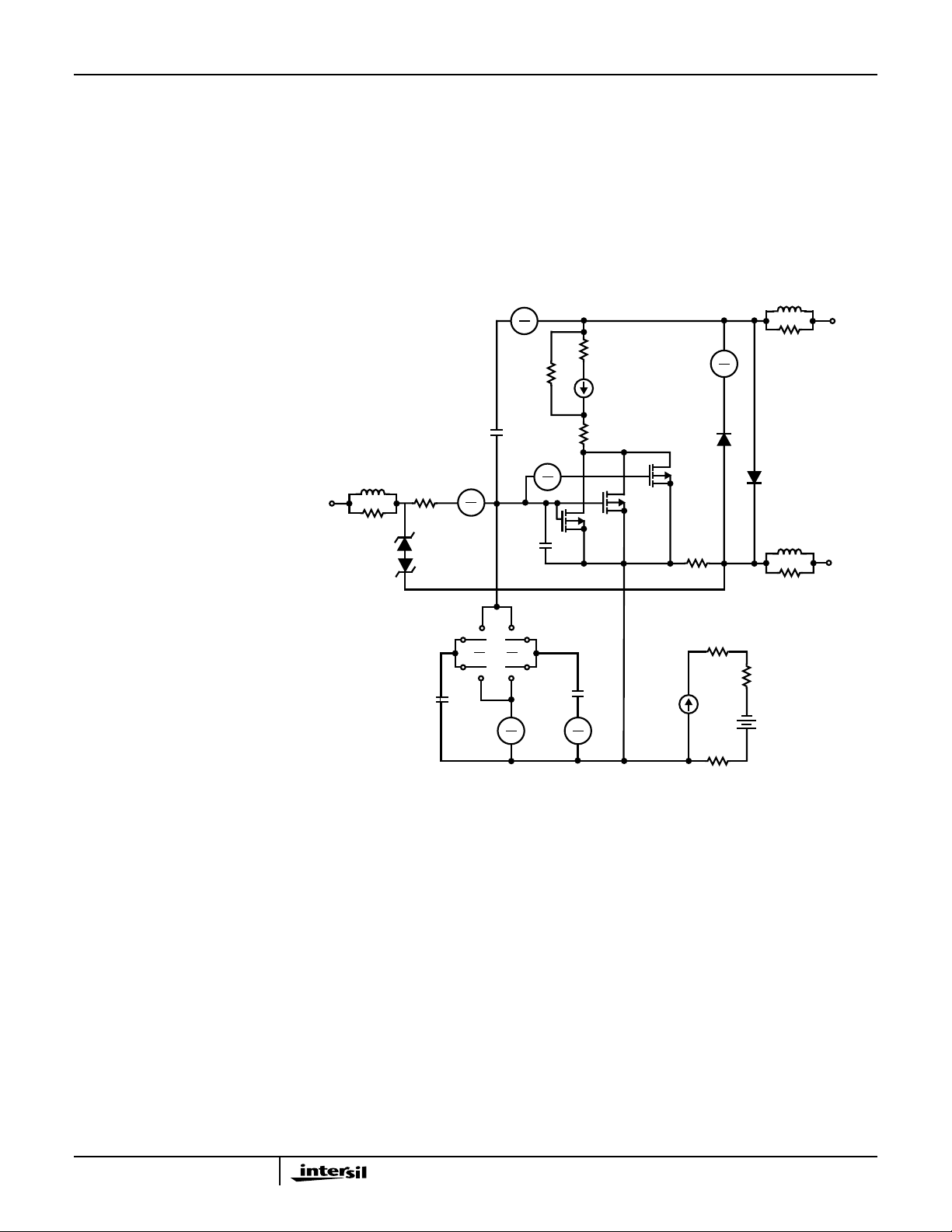
SABER Electrical Model
REV Dec 1999
template itf87072dk8 n2,n1,n3
electrical n2,n1,n3
{
var i iscl
dp..model dbodymod = (isl = 1.7e-10, ikf = 3, nl = 1.18, cjo = 6e-10, tt = 5.1e-9, m = 0.47, rs = 1.05e-2, trs1 = 1.75e-3, trs2 = 5.08e-6)
dp..model dbreakmod = (rs = 4e-1, trs1 = 1e-3, trs2 = -2e-5)
dp..model desd1mod = (bv = 9.5, tbv1 = -2.9e-3, nl = 12, rs = 35)
dp..model desd2mod = (bv = 10.2, tb1 = -2.5e-3, nl = 13, rs = 35)
dp..model dplcapmod = (cjo = 4.7e-10, isl = 10e-30, nl = 10, m = 0.4, vj = 0.45)
m..model mmedmod = (type=_p, vto = -1.15, kp = 23, is = 1e-30, tox = 1, rs = 0.1)
m..model mstrongmod = (type=_p, vto = -1.35, kp = 30, lambda = 0.05, is = 1e-30, tox = 1)
m..model mweakmod = (type=_p, vto = -0.82, kp = 0.06, is = 1e-30, tox = 1, rs = 0.1)
sw_vcsp..model s1amod = (ron = 1e-5, roff = 0.1, von = 2.5, voff = 1.5)
sw_vcsp..model s1bmod = (ron =1e-5, roff = 0.1, von = 1.5, voff = 2.5)
sw_vcsp..model s2amod = (ron = 1e-5, roff = 0.1, von = 0.75, voff = -0.5)
sw_vcsp..model s2bmod = (ron = 1e-5, roff = 0.1, von = -0.5, voff = 0.75)
c.ca n12 n8 = 1.15e-9
c.cb n15 n14 = 1.2e-9
c.cin n6 n8 = 1.09e-9
dp.dbody n5 n7 = model=dbodymod
dp.dbreak n7 n11 = model=dbreakmod
DPLCAP
dp.desd1 n91 n9 = model=desd1mod
dp.desd2 n91 n7 = model=desd2mod
dp.dplcap n10 n6 = model=dplcapmod
i.it n8 n17 = 1
GATE
l.ldrain n2 n5 = 1e-9
l.lgate n1 n9 = 3.6e-9
l.lsource n3 n7 = 4.3e-9
m.mmed n16 n6 n8 n8 = model=mmedmod, l=1u, w=1u
m.mstrong n16 n6 n8 n8 = model=mstrongmod, l=1u, w=1u
m.mweak n16 n21 n8 n8 = model=mweakmod, l=1u, w=1u
res.rbreak n17 n18 = 1, tc1 = 9e-4, tc2 = 1e-6
res.rdrain n50 n16 = 5.8e-3, tc1 = 1.2e-2, tc2 = 1.2e-6
res.rgate n9 n20 = 16.1
res.rldrain n2 n5 = 10
res.rlgate n1 n9 = 36
LGATE
1
RLGATE
91
RGATE
9
DESD1
DESD2
CA
EVTEMP
-
18
22
20
S1A
12
S1B
res.rlsource n3 n7 = 43
res.rslc1 n5 n51 = 1e-6, tc1 = 1e-3, tc2 = 1e-6
res.rslc2 n5 n50 = 1e3
res.rsource n8 n7 = 1.1e-2, tc1 = 0, tc2 = 5e-6
res.rvtemp n18 n19 = 1, tc1 = -4e-4, tc2 = -1e-7
res.rvthres n22 n8 = 1, tc1 = 1.3e-3, tc2 = 2.3e-6
spe.ebreak n5 n11 n17 n18 = -29.6
spe.eds n14 n8 n5 n8 = 1
spe.egs n13 n8 n6 n8 = 1
spe.esg n5 n10 n8 n6 = 1
spe.evtemp n6 n20 n18 n22 = 1
spe.evthres n6 n21 n19 n8 = 1
sw_vcsp.s1a n6 n12 n13 n8 = model=s1amod
sw_vcsp.s1b n13 n12 n13 n8 = model=s1bmod
sw_vcsp.s2a n6 n15 n14 n13 = model=s2amod
sw_vcsp.s2b n13 n15 n14 n13 = model=s2bmod
v.vbat n22 n19 = dc=1
equations {
i (n51->n50) +=iscl
iscl: v(n51,n50) = ((v(n5,n51)/(1e-9+abs(v(n5,n51))))*((abs(v(n5,n51)*1e6/100))** 2.1))
}
}
ESG
+
-
8
6
10
RSLC2
EVTHRES
+
19
8
6
+
S2A
13
14
8
13
S2B
13
+
+
6
EGS EDS
8
-
-
15
CIN
CB
-
+
5
8
-
5
RSLC1
51
50
RDRAIN
21
MSTRO
14
ISCL
16
8
EBREAK
MMED
RSOURCE
IT
8
+
17
18
-
11
DBREAK
MWEAK
7
RBREAK
17 18
RVTHRES
-
+
22
LDRAIN
RLDRAIN
DBODY
LSOURCE
RLSOURCE
RVTEMP
19
VBAT
DRAIN
2
SOURCE
3
10
Page 11
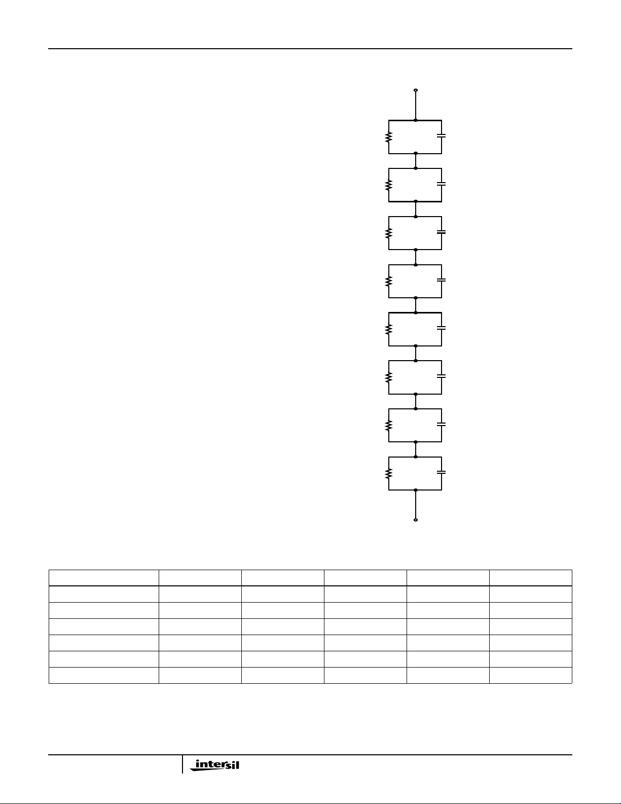
SPICE Thermal Model
REV April 1999
ITF87072DK8
Copper Area = 0.02 in
CTHERM1 th 8 8.5e-4
CTHERM2 8 7 1.8e-3
CTHERM3 7 6 5.0e-3
CTHERM4 6 5 1.3e-2
CTHERM5 5 4 4.0e-2
CTHERM6 4 3 9.0e-2
CTHERM7 3 2 4.0e-1
CTHERM8 2 tl 1.4
2
ITF87072DK8T
RTHERM1
RTHERM2
th
JUNCTION
CTHERM1
8
CTHERM2
RTHERM1 th 8 3.5e-2
RTHERM2 8 7 6.0e-1
RTHERM3 7 6 2
RTHERM4 6 5 8
RTHERM5 5 4 18
RTHERM6 4 3 39
RTHERM7 3 2 42
RTHERM8 2 tl 48
SABER Thermal Model
Copper Area = 0.02 in
template thermal_model th tl
thermal_c th, tl
{
ctherm.ctherm1 th 8 = 8.5e-4
ctherm.ctherm2 8 7 = 1.8e-3
ctherm.ctherm3 7 6 = 5.0e-3
ctherm.ctherm4 6 5 = 1.3e-2
ctherm.ctherm5 5 4 = 4.0e-2
ctherm.ctherm6 4 3 = 9.0e-2
ctherm.ctherm7 3 2 = 4.0e-1
ctherm.ctherm8 2 tl = 1.4
rtherm.rtherm1 th 8 = 3.5e-2
rtherm.rtherm2 8 7 = 6.0e-1
rtherm.rtherm3 7 6 = 2
rtherm.rtherm4 6 5 = 8
rtherm.rtherm5 5 4 = 18
rtherm.rtherm6 4 3 = 39
rtherm.rtherm7 3 2 = 42
rtherm.rtherm8 2 tl = 48
}
2
RTHERM3
RTHERM4
RTHERM5
RTHERM6
RTHERM7
RTHERM8
7
CTHERM3
6
CTHERM4
5
CTHERM5
4
CTHERM6
3
CTHERM7
2
CTHERM8
tl
AMBIENT
TABLE 1. THERMAL MODELS
COMPONENT 0.02 in
2
0.14 in
2
0.257 in
2
0.38 in
2
0.493 in
CTHERM6 9.0e-2 1.3e-1 1.5e-1 1.5e-1 1.5e-1
CTHERM7 4.0e-1 6.0e-1 4.5e-1 6.5e-1 7.5e-1
CTHERM8 1.4 2.5 2.2 3 3
RTHERM6 39 26 20 20 20
RTHERM7 42 32 31 29 23
RTHERM8 48 35 38 31 25
11
2
Page 12
ITF87072DK8T
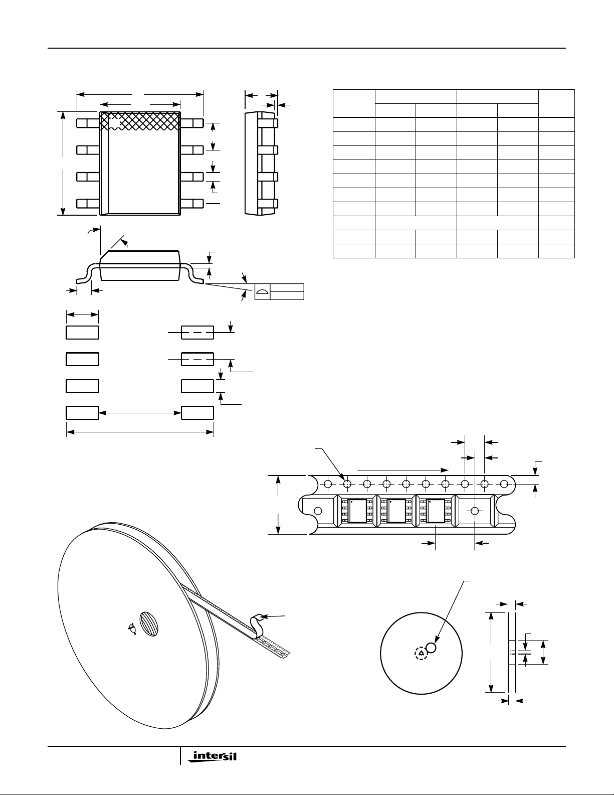
MS-012AA
8 LEAD JEDEC MS-012AA SMALL OUTLINE PLASTIC PACKAGE
E
E
1
1
2
D
56
o
h x 45
L
0.060
1.52
0.155
4.0
0.275
7.0
MINIMUM RECOMMENDED FOOTPRINT FOR
SURFACE-MOUNTED APPLICATIONS
A
A
1
SYMBOL
INCHES MILLIMETERS
NOTESMIN MAX MIN MAX
A 0.0532 0.0688 1.35 1.75 -
e
A
1
0.004 0.0098 0.10 0.25 b 0.013 0.020 0.33 0.51 c 0.0075 0.0098 0.19 0.25 -
D 0.189 0.1968 4.80 5.00 2
b
E 0.2284 0.244 5.80 6.20 -
E
1
0.1497 0.1574 3.80 4.00 3
e 0.050 BSC 1.27 BSC -
H 0.0099 0.0196 0.25 0.50 -
c
L 0.016 0.050 0.40 1.27 4
NOTES:
1. All dimensions are within allowable dimensions of Rev. C of
JEDEC MS-012AA outline dated 5-90.
2. Dimension “D” does not include mold flash, protrusions or gate
burrs. Mold flash, protrusions or gate burrs shall not exceed
0o-8
0.004 IN
0.10 mm
o
0.006 inches (0.15mm) per side.
3. Dimension “E1” does not include inter-lead flash or protrusions.
Inter-lead flash and protrusions shall not exceed 0.010 inches
(0.25mm) per side.
0.050
1.27
4. “L” is the length of terminal for soldering.
5. The chamfer on the body is optional. If it is not present, a visual index
feature must be located within the crosshatched area.
0.024
0.6
1.5mm
DIA. HOLE
6. Controlling dimension: Millimeter.
7. Revision 8 dated 5-99.
4.0mm
USER DIRECTION OF FEED
2.0mm
1.75mm
MS-012AA
12mm TAPE AND REEL
12
12mm
COVER TAPE
GENERAL INFORMATION
1. 2500 PIECES PER REEL.
2. ORDER IN MULTIPLES OF FULL REELS ONLY.
3. MEETS EIA-481 REVISION “A” SPECIFICATIONS.
8.0mm
40mm MIN.
ACCESS HOLE
330mm
C
L
18.4mm
13mm
12.4mm
50mm
Page 13

ITF87072DK8T
All Intersil semiconductor products are manufactured, assembled and tested under ISO9000 quality systems certification.
Intersil semiconductor products are sold by description only. Intersil Corporation reserves the right to make changes in circuit design and/or specifications at any time without notice. Accordingly, the reader is cautioned to verify that data sheets are current before placing orders. Information furnished by Intersil is believed to be accurate and
reliable. However, no responsibility is assumed by Intersil or its subsidiaries for its use; nor for any infringements of patents or other rights of third parties which may result
from its use. No license is granted by implication or otherwise under any patent or patent rights of Intersil or its subsidiaries.
For information regarding Intersil Corporation and its products, see web site www.intersil.com
Sales Office Headquarters
NORTH AMERICA
Intersil Corporation
P. O. Box 883, Mail Stop 53-204
Melbourne, FL 32902
TEL: (321) 724-7000
FAX: (321) 724-7240
13
EUROPE
Intersil SA
Mercure Center
100, Rue de la Fusee
1130 Brussels, Belgium
TEL: (32) 2.724.2111
FAX: (32) 2.724.22.05
ASIA
Intersil (Taiwan) Ltd.
7F-6, No. 101 Fu Hsing North Road
Taipei, Taiwan
Republic of China
TEL: (886) 2 2716 9310
FAX: (886) 2 2715 3029
 Loading...