

Page 1
ITA6V5B1 / ITA10B1
ApplicationSpecific Discretes
A.S.D.
APPLICATIONS
Differentialdatatransmission lines protection:
-RS-232
-RS-423
-RS-422
-RS-485
FEATURES
HIGH SURGE CAPABILITY TRANSIL ARRAY
= 40 A (8/20µs)
I
PP
PEAKPULSEPOWER : 300 W (8/20µs)
UPTO5BIDIREC T ION ALTRANSILFUNC TIONS
LOWCLAMPINGFACTOR(V
CURRENT LEVEL
LOWLEAKAGECURRENT
ESDPROTECTION UP TO 15kV
TM
CL/VBR
BIDIRECTIONALTRANSIL
) ATHIGH
ITA18B1 / ITA25B1
TM
ARRAY
FOR DATALINE PROTECTION
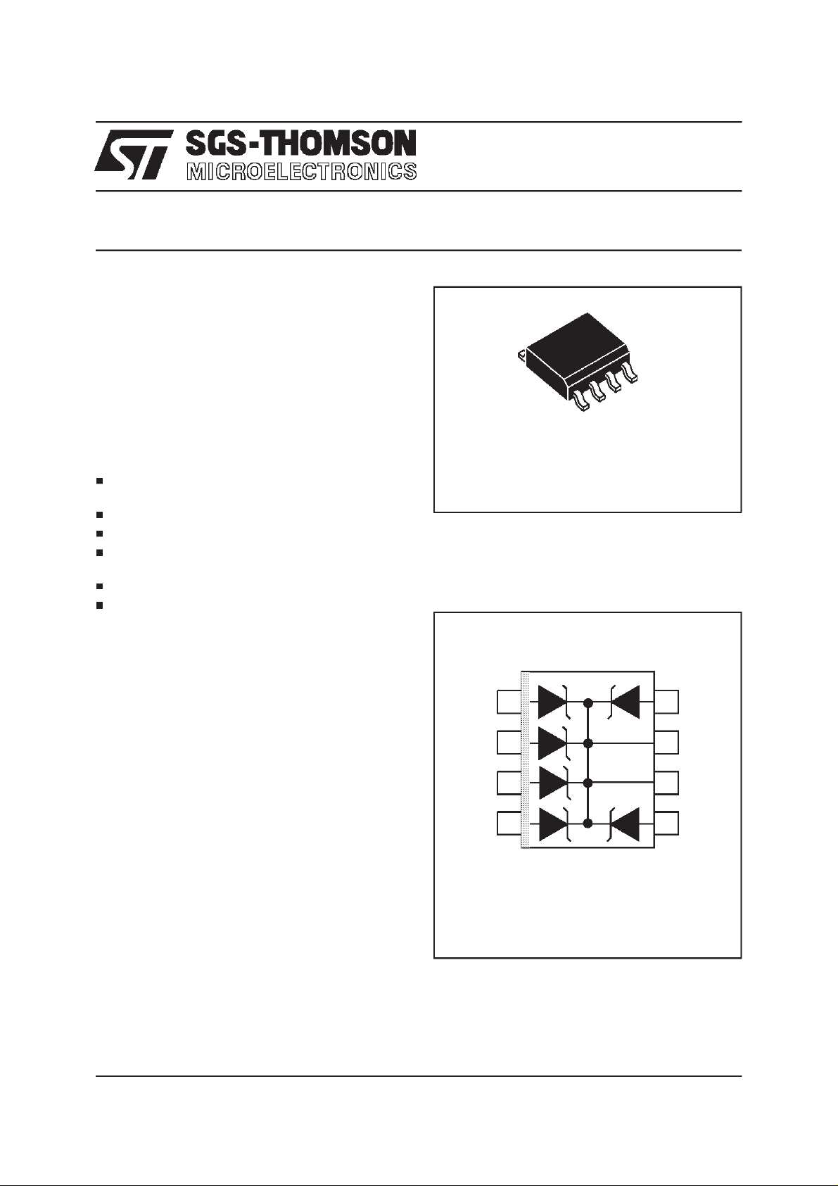
SO8
FUNCTIONALDIAGRAM
DESCRIPTION
Transil diode arrays provide high overvoltage
protectionby clamping action.Theirinstantaneous
response to transient overvoltages makes them
particularly suited to protect voltage sensitive
devicessuch as MOS Technologyand low voltage
suppliedIC’s.
The ITA series allies highsurge capabilityagainst
energetic pulses with high voltage performance
againstESD.
COMPLIESWITHTHEFOLLOWINGSTAN DAR DS:
IEC1000-4-2: level 4
IEC1000-4-4: level 4
IEC1000-4-5: level 2
MILSTD 883C - Method3015-6: class3
(humanbodymodel)
January 1998 Ed: 2
I/O
2
I/O
I/O 3
I/O 4
1
1
2
3
4
8
7
6
5
GND
GND
1/5
Page 2
ITA6V5B1 / ITA10B1/ ITA18B1 / ITA25B1
ABSOLUTE MAXIMUMRATINGS(T
amb
=25°C)
Symbol Parameter Value Unit
P
PP
Peak pulsepower dissipation (8/20µs)
Tjinitial= T
amb
300 W
(see note1)
I
PP
2
t Wire I2t value (seenote 1) 0.6 A2s
I
T
stg
T
j
T
L
Note 1 : For surges greater than the specified maximum
value, the I/O will first present a short-circuit and after an
opencircuit caused by the wire melting.
ELECTRICALCHARACTERISTICS(T
Peak pulsecurrent (8/20µs)(see note 1) Tjinitial= T
amb
Storagetemperaturerange
Maximumoperatingjunction temperature
Maximumlead temperaturefor solderingduring10s 260 °C
%I
pp
8s
Pulse wave form 8/20 s
20 s
amb
100
50
0
=25°C)
40 A
- 55 to +150
125
t
°C
°
C
Symbol Parameter
V
RM
V
BR
V
CL
I
RM
I
PP
α
T Voltagetemperaturecoefficient
Stand-offvoltage
Breakdownvoltage
Clampingvoltage
Leakagecurrent @ V
Peak pulsecurrent
RM
C Junctioncapacitance
Types IRM@V
max. min. 8/20µs max. 8/20µs max. max.
AV VmAV A V A10
µ
ITA6V5B1
ITA10B1
ITA18B1
ITA25B1
Note 2 :BetweenI/Opin and ground.
Note 3 :Betweentwo input Pins at 0V Bias, F = 1 MHz.
Preferredtypes in bold
10 5 6.5 1 10 10 12 25 4 750
4 8 10 1 15 10 19 25 8 570
4 15 18 1 25 10 28 25 9 350
4 24 25 1 33 10 38 25 12 300
RM
VBR@I
note 2 note 2 note 2 note 3
R
VCL@I
PP
VCL@I
PP
αTC
-4
/°CpF
2/5
Page 3

ITA6V5B1 / ITA10B1/ ITA18B1/ITA25B1
Fig. 1 :
Typical peak pulse power versus
exponentialpulse duration.
P(W)
P
1E+04
1E+03
1E+02
1E+01
Fig. 3 :
P
Tinitial=25C
j
ITA25B1 ITA18B1
ITA10B1ITA6V5B1
t (ms) expo
P
1E-03 1E-02 1E-01 1E+00 1E+01 1E+02
Peak current I
inducing open circuit of
DC
o
thewire for one input/outputversuspulseduration
(typicalvalues).
I (A)
DC
1E+03
exponential waveform
Fig. 2 : Clamping voltage versus peak pulse
current(exponentialwaveform 8/20 µs).
Fig. 4 :
Junction capacitance versus reverse
applied voltage for one input/output (typical
values).
1E+02
1E+01
1E+00
1E-02 1E-01 1E+00 1E+01
t (ms)
Fig.5 : Relative variation of leakage current
versus junction temperature
3/5
Page 4

ITA6V5B1 / ITA10B1/ ITA18B1 / ITA25B1
APPLICATION INFORMATION
Types Maximum differential voltage
ITA6V5B1
ITA10B1
ITA18B1
ITA25B1
between two input pins at 25°C
+/ - 3.5 V
+/ - 5.0 V
+/ - 9.0 V
+ / - 12.5 V
Typicalapplication: RS232junction.
This monolithic Transil Array is based on 6
unidirectionalTransilswith a commoncathode and
can be configurated to offer up to 5 bidirectional
functions. This imposes a maximum differential
voltagebetween2 inputpins (see oppositetable).
TX
RX
RTS
CTS
GND
ORDERCODE
INTEGRATED
TRANSILARRAY
4/5
ITA 25 B 1 RL
PACKAGING:
RL = Tapeand reel.
= Tube.
PACKAGE : SO8 PLASTIC
min
V
BR
BIDIRECTIONAL
Page 5

MARKING
TYPE MARKING
ITA6V5B1 6V5B1
ITA10B1 10B1
ITA18B1 18B1
ITA25B1 25B1
PACKAGEMECHANICALDATA
SO8 (Plastic)
ITA6V5B1 / ITA10B1/ ITA18B1/ITA25B1
DIMENSIONS
REF.
A 1.75 0.069
a1 0.1 0.25 0.004 0.010
a2 1.65 0.065
b 0.35 0.48 0.014 0.019
b1 0.19 0.25 0.007 0.010
C 0.50 0.020
c1 45°(typ)
D 4.8 5.0 0.189 0.197
E 5.8 6.2 0.228 0.244
e 1.27 0.050
e3 3.81 0.150
F 3.8 4.0 0.15 0.157
L 0.4 1.27 0.016 0.050
M 0.6 0.024
S8
Millimetres Inches
Min. Typ. Max. Min. Typ. Max.
°
(max)
Packaging:Preferred packagingistapeand reel.
Weight: 0.08g.
Information furnished is believed to be accurate and reliable. However, SGS-THOMSON Microelectronics assumes no responsibility for the
consequences of use of such information nor for any infringement of patents or other rights of third parties whichmay result from its use. No
license is grantedby implication or otherwise under any patentor patent rights of SGS-THOMSON Microelectronics.Specifications mentioned
in this publication are subject to change without notice. This publication supersedes and replaces all information previously supplied. SGSTHOMSON Microelectronics productsare not authorizedfor useas criticalcomponents in life support devicesor systems withoutexpress written approval of SGS-THOMSON Microelectronics.
1998 SGS-THOMSON Microelectronics - Printed in Italy - All rights reserved.
SGS-THOMSON Microelectronics GROUP OF COMPANIES
Australia- Brazil- Canada - China- France- Germany- Italy- Japan- Korea- Malaysia - Malta- Morocco
TheNetherlands - Singapore- Spain- Sweden- Switzerland- Taiwan- Thailand- UnitedKingdom - U.S.A.
5/5
 Loading...