

Datasheet ISPLSI8840-60LB432, ISPLSI8840-110LB432 Datasheet (Lattice Semiconductor Corporation)
Page 1
®
ispLSI
8840
In-System Programmable
SuperBIG™ High Density PLD
Features
• SuperBIG HIGH DENSITY IN-SYSTEM
PROGRAMMABLE LOGIC
— 5V Power Supply
— 45,000 PLD Gates/840 Macrocells
— Up to 312 I/O Pins Supporting 3.3V/5V I/O
— 1152 Registers
— High-Speed Global and Big Fast Megablock (BFM)
Interconnect
— Wide 20-Macrocell Generic Logic Block (GLB) for
High Performance
— Wide Input Gating (44 Inputs per GLB) for Fast
Counters, State Machines, Address Decoders, Etc.
— PCB-Efficient Ball Grid Array (BGA) Package
Options
2
• HIGH-PERFORMANCE E
—
fmax = 110 MHz Maximum Operating Frequency
tpd = 8.5 ns Propagation Delay
—
— TTL Compatible Inputs and 3.3V/5V Outputs
— PCI Compatible Inputs, Outputs and Speed Grades
— Electrically Erasable and Reprogrammable
— Non-Volatile
— Programmable Speed/Power Logic Path
Optimization
• IN-SYSTEM PROGRAMMABLE
— Increased Manufacturing Yields, Reduced Time-to-
Market and Improved Product Quality
— Reprogram Soldered Devices for Faster Debugging
• 100% IEEE 1149.1 BOUNDARY SCAN TESTABLE AND
5V IN-SYSTEM PROGRAMMABLE
• ARCHITECTURE FEATURES
— Enhanced Pin-Locking Architecture, Symmetrical
Generic Logic Blocks Connected by Hierarchical
Big Fast Megablock and Global Routing Planes
— Product Term Sharing Array Supports up to 28
Product Terms per Macrocell Output
— Macrocells Support Concurrent Combinatorial and
Registered Functions
— Embedded Tristate Bus Can Be Used as an Internal
Tristate Bus or as an Extension of an External
Tristate Bus
— Macrocell and I/O Registers Feature Multiple Control
Options, Including Set, Reset and Clock Enable
— I/O Pins Support Programmable Bus Hold, Pull-Up,
Open-Drain and Slew Rate Options
— Separate VCCIO Power Supply for Output Drivers
Supports 5V or 3.3V Outputs
— I/O Cell Register Programmable as Input Register for
Fast Setup Time or Output Register for Fast Clock to
Output Time
CMOS® TECHNOLOGY
• ispDesignEXPERT™ – LOGIC COMPILER AND COMPLETE ISP DEVICE DESIGN SYSTEMS FROM HDL
SYNTHESIS THROUGH IN-SYSTEM PROGRAMMING
— Superior Quality of Results
— Tightly Integrated with Leading CAE Vendor Tools
— Productivity Enhancing Timing Analyzer, Explore
Tools, Timing Simulator and ispANALYZER™
— PC and UNIX Platforms
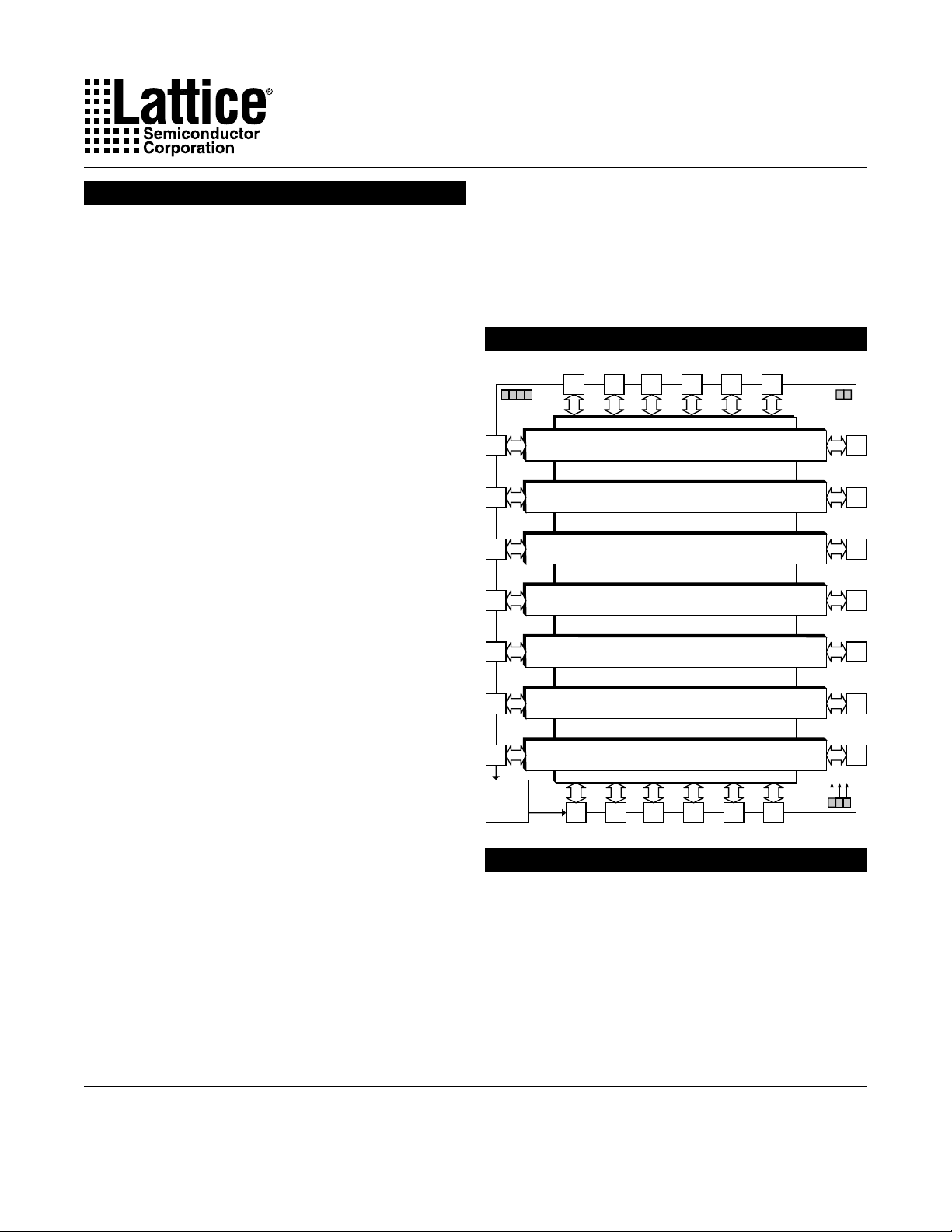
Functional Block Diagram
12
I/O
12
I/O
12
I/O
12
I/O
12
I/O
12
I/O
12
I/O
Boundary
Scan
12
I/O
12
I/O
12
12
I/O
Big Fast Megablock 0
Big Fast Megablock 1
Big Fast Megablock 2
Global Routing Plane
Big Fast Megablock 3
Big Fast Megablock 4
Big Fast Megablock 5
Big Fast Megablock 6
12
I/O
I/O
12
I/O
12
I/O12I/O12I/O
12
I/O12I/O12I/O
8840 block
12
I/O
12
I/O
12
I/O
12
I/O
12
I/O
12
I/O
12
I/O
ispLSI 8000 Family Description
The ispLSI 8000 Family of Register-Intensive, SuperBIG
In-System Programmable Logic Devices is based on Big
Fast Megablocks of 120 registered macrocells and a
Global Routing Plane (GRP) structure interconnecting
the Big Fast Megablocks. Each Big Fast Megablock
contains 120 registered macrocells arranged in six groups
of 20, a group of 20 being referred to as a Generic Logic
Block, or GLB. Within the Big Fast Megablock, a Big Fast
Megablock Routing Pool (BRP) interconnects the six
GLBs to each other and to 24 Big Fast Megablock I/O
Copyright © 2000 Lattice Semiconductor Corp. All brand or product names are trademarks or registered trademarks of their respective holders. The specifications and information herein are subject
to change without notice.
LATTICE SEMICONDUCTOR CORP., 5555 Northeast Moore Ct., Hillsboro, Oregon 97124, U.S.A.
January 2000
Tel. (503) 268-8000; 1-800-LATTICE; FAX (503) 268-8556; http://www.latticesemi.com
8840_07 1
Page 2
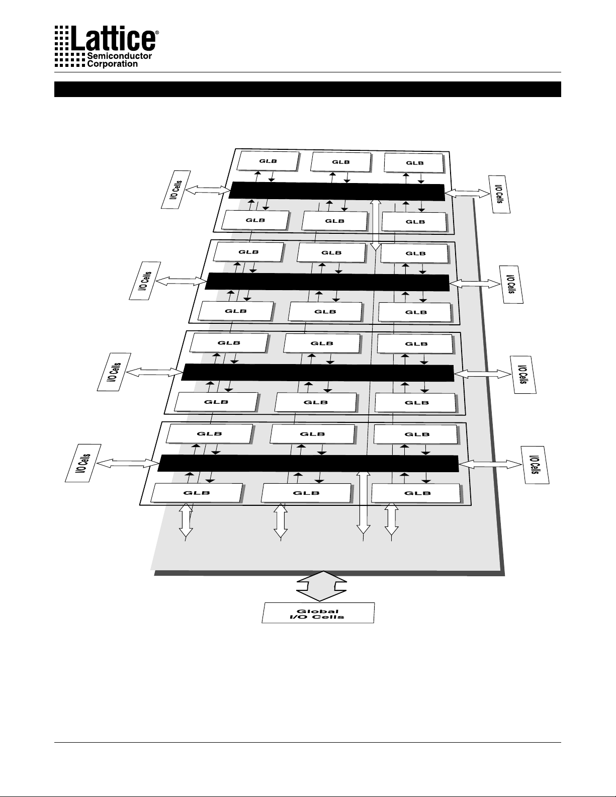
Functional Block Diagram
Figure 1. ispLSI 8840 Functional Block Diagram (Perspective)
Big Fast Megablock Routing Pool (BRP)
Big Fast Megablock Routing Pool (BRP)
Specifications ispLSI 8840
Big Fast Megablock Routing Pool (BRP)
Big Fast Megablock Routing Pool (BRP)
Global Routing Plane (GRP) with Tristate Bus Lines
2
Page 3

ispLSI 8000 Family Description (Continued)
Specifications ispLSI 8840
cells with optional I/O registers. The Global Routing
Plane which interconnects the Big Fast Megablocks has
an additional 144 global I/Os with optional I/O registers.
Outputs from the GLBs in a Big Fast Megablock can drive
both the Big Fast Megablock Routing Pool within the Big
Fast Megablock and the Global Routing Plane between
the Big Fast Megablocks. Switching resources are provided to allow signals in the Global Routing Plane to drive
any or all the Big Fast Megablocks in the device. This
mechanism allows fast, efficient connections, both within
the Big Fast Megablocks and between them.
Each GLB contains 20 macrocells and a fully populated,
programmable AND-array with 82 logic product terms.
The GLB has 44 inputs from the Big Fast Megablock
Routing Pool which are available in both true and complement form for every product term. Up to 20 of these inputs
can be switched to provide local feedback into the GLB
for logic functions that require it. The 80 general-purpose
product terms can be grouped into 20 sets of four and
sent into a Product Term Sharing Array (PTSA) which
allows sharing up to a maximum of 28 product terms for
a single function. Alternatively, the PTSA can be bypassed for functions of four product terms or less.
The 20 registered macrocells in the GLB are driven by the
20 outputs from the PTSA or the PTSA bypass. Each
macrocell contains a programmable XOR gate, a programmable register/latch/toggle flip-flop and the
necessary clocks and control logic to allow combinatorial
or registered operation. Each macrocell has two outputs,
one output can be fed back inside the GLB to the ANDarray, while the other output drives both the Big Fast
Megablock Routing Pool and the Global Routing Plane.
This dual output capability from the macrocell allows
efficient use of the hardware resources. One output can
be a registered function for example, while the other
output can be an unrelated combinatorial function.
Macrocell registers can be clocked from one of several
global, local or product term clocks available on the
device. A global, local and product term clock enable is
also provided, eliminating the need to gate the clock to
the macrocell registers. Reset and preset for the macrocell
register is provided from both global and product term
signals. The polarity of all of these control signals is
selectable on an individual macrocell basis. The macrocell register can be programmed to operate as a D-type
register, a D-type flow-through latch or a T-type flip flop.
The 20 outputs from the GLB can drive both the Big Fast
Megablock Routing Pool within the Big Fast Megablock
and the Global Routing Plane between the Big Fast
Megablocks. The Big Fast Megablock Routing Pool contains general purpose tracks which interconnect the six
GLBs within the Big Fast Megablock and dedicated
tracks for the signals from the Big Fast Megablock I/O
cells. The Global Routing Plane contains general purpose tracks that interconnect the Big Fast Megablocks
and also carry the signals from the I/Os connected to the
Global Routing Plane.
Control signals for the I/O cell registers are generated
using an extra product term within each GLB, or using
dedicated input pins. Each GLB has two extra product
terms beyond the 80 available for the macrocell logic.
The first additional product term is used as an optional
shared product term clock for all the macrocells within the
GLB. The second additional product term is then routed
to an I/O Control Bus using a separate routing structure
from the Big Fast Megablock Routing Pool and Global
Routing Plane. Use of a separate control bus routing
structure allows the I/O registers to have many control
signals with no impact on the interconnection of the GLBs
and Big Fast Megablocks. The I/O Control Bus is split into
four quadrants, each servicing the I/O cell control requirements for one edge of the device. Signals in the
control bus can be independently selected by any or all
I/O cells to act as clock, clock enable, output enable,
reset or preset.
Each Big Fast Megablock has 24 I/O cells. The Global
Routing Pool has 144 I/O cells. Each I/O cell can be
configured as a combinatorial input, combinatorial output, registered input, registered output or bidirectional
I/O. I/O cell registers can be clocked from one of several
global, local or product term clocks which are selected
from the I/O control bus. A global and product term clock
enable is also provided, eliminating the need for the user
to gate the clock to the I/O cell registers. Reset and preset
for the I/O cell register is provided from both global and
product term signals. The polarity of all of these control
signals is selectable on an individual I/O cell basis. The
I/O cell register can be programmed to operate as a Dtype register or a D-type latch.
Inputs and outputs are PCI compatible. The input threshold is fixed at TTL levels. The output driver can source
4mA and sink 8mA. The output drivers have a separate
VCCIO power supply which is independent of the main
VCC supply for the device. This feature allows the output
drivers to run from either 5V or 3.3V while the device logic
is always powered from 5V. The output drivers also
provide individually programmable edge rates and open
3
Page 4

Specifications ispLSI 8840
ispLSI 8000 Family Description (Continued)
drain capability. A programmable pullup resistor is provided to tie off unused inputs and a programmable
bus-hold latch is available to hold tristate outputs in their
last valid state until the bus is driven again by another
device.
The ispLSI 8000 Family features 5V, non-volatile insystem programmability for both the logic and the
interconnect structures, providing the means to develop
truly reconfigurable systems. Programming is achieved
through the industry standard IEEE 1149.1-compliant
Boundary Scan interface using either the JTAG protocol
or Lattice proprietary ISP protocol. Boundary Scan test is
also supported through the same interface.
An enhanced, multiple cell security scheme is provided
that prevents reading of the JEDEC programming file
when secured. After the device has been secured using
this mechanism, the only way to clear the security is to
execute a bulk-erase instruction.
ispLSI 8840 Description
The ispLSI 8840 device has seven Big Fast Megablocks
for a total of 7 x 120 = 840 macrocells.
Each Big Fast Megablock has a total of 24 I/O cells and
the Global Routing Plane has a total of 144 I/O cells. This
gives (7 x 24) + 144 = 312 I/Os.
participate in driving the embedded tristate bus. The
remaining two macrocells per GLB are used to generate
the internal tristate driver control signals on each data
byte (with parity). The embedded tristate bus can also be
configured as an extension of an external tristate bus
using the bidirectional capability of the I/O cells connected to the Global Routing Plane. The Global Routing
Plane I/Os 0-8 and 15-23 from each group (I/OGx as
defined in the I/O Pin Location Table) can connect to the
internal tristate bus as well as the unidirectional/nontristate global routing channels. I/Os 9-14 connect only to
the global routing channel.
The embedded tristate bus has internal bus hold and
arbitration features in order to make the function more
“user friendly”. The bus hold feature keeps the internal
bus at the previously driven logic state when the bus is
not driven to eliminate bus float. The bus arbitration is
performed on a “first come, first served” priority. In other
words, once a logic block drives the bus, other logic
blocks cannot drive the bus until the first releases the bus.
This arbitration feature prevents internal bus contention
when there is an overlap between two bus enable signals. Typically, it takes about 3ns to resolve one bus
signal coming off the bus to another bus signal driving the
bus. The arbitration feature combined with the predictability of CPLD, makes the embedded tristate bus the
most practical for the real world bus implementations.
The total registers in the device is the sum of macrocells
plus I/O cells, 840 + 312 = 1152 registers.
Embedded Tristate Bus
There is a 108-line embedded internal tristate bus as part
of the Global Routing Plane (GRP), enabling multiple
GLBs to drive the same tracks. This bus can be partitioned into various bus widths such as twelve 9-line
buses, six 18-line buses or three 36-line buses. The
GLBs can dynamically share a subset of the Global
Routing Plane tracks. This feature eliminates the need to
convert tristate buses to wide multiplexers on the programmable device. Up to 18 macrocells per GLB can
4
Page 5
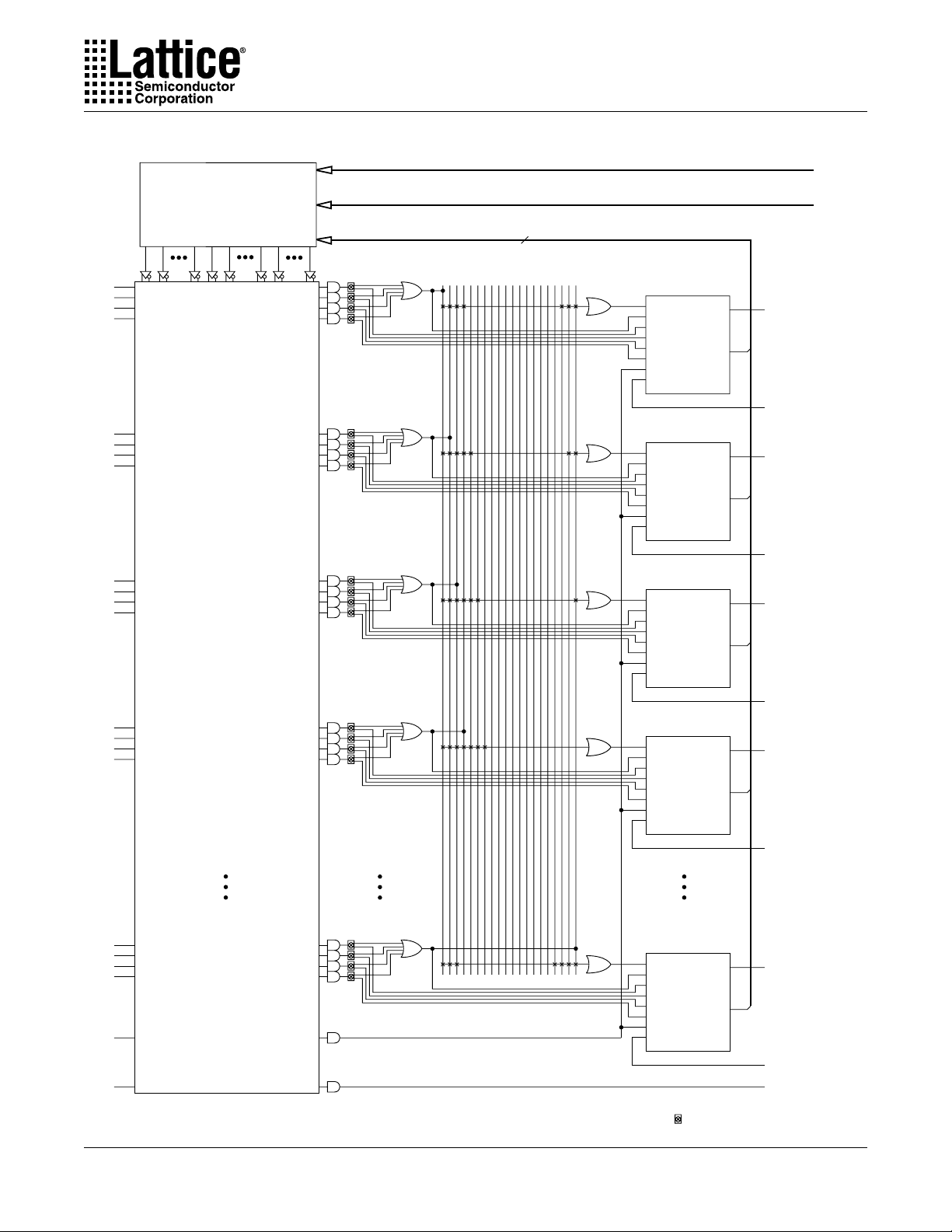
Figure 2. ispLSI 8000 GLB Overview
I/O Big Fast Megablock Input Tracks
Specifications ispLSI 8840
PT 0
PT 1
PT 2
PT 3
PT 4
PT 5
PT 6
PT 7
PT 8
PT 9
PT 10
PT 11
AND Array Input
0
Fully Populated
Routing
AND Array
General Purpose Big Fast Megablock Input Tracks
Feedback Inputs
43
Product Term
Sharing Array
20
Macrocell 0
From PTSA
PTSA Bypass
Single PT
PT Clock
PT Preset
PT Reset
Shared PT Clock
Bus Input
Macrocell 1
From PTSA
PTSA Bypass
Single PT
PT Clock
PT Preset
PT Reset
Shared PT Clock
Bus Input
Macrocell 2
From PTSA
PTSA Bypass
Single PT
PT Clock
PT Preset
PT Reset
Shared PT Clock
Bus Input
0
1
2
To Interconnect
From Tristate
Bus Track
To Interconnect
From Tristate
Bus Track
To Interconnect
PT 12
PT 13
PT 14
PT 15
PT 76
PT 77
PT 78
PT 79
PT 80
PT 81
Macrocell 3
From PTSA
PTSA Bypass
Single PT
PT Clock
PT Preset
PT Reset
Shared PT Clock
Bus Input
Macrocell 19
From PTSA
PTSA Bypass
Single PT
PT Clock
PT Preset
PT Reset
Shared PT Clock
Bus Input
Function Selector (E2 Cell Controlled)Note: Macrocells 9 and 10 do not support Tristate Bus Feedback.
From Tristate
Bus Track
To interconnect
3
From Tristate
Bus Track
To Interconnect
19
From Tristate Bus Track
To Output Control MUX
5
Page 6
Figure 3. ispLSI 8000 Macrocell Overview
Single PT
PTSA
PTSA Bypass
PT Clock
Global Clock Enable
Global Clock 0
Global Clock 1
Global Clock 2
PT Reset
GRST
PT Preset
Specifications ispLSI 8840
Bus Input From Tristate
Bus Track*
Feedback to AND Array
DQ
To Big Fast Megablock
or Global Interconnect
Clk En
RP
R/L
From Macrocell
9 or 10
To Specific
Global Tristate Bus*
Macrocells 0-8
and 11-19
Reset pin
Preset/Reset Input has Global Polarity Control
GRST
To All Macrocells and I/O Cells
From PT80
: Function Selector (E2 Cell Controlled)*Not available for Macrocells 9 and 10.
6
Page 7
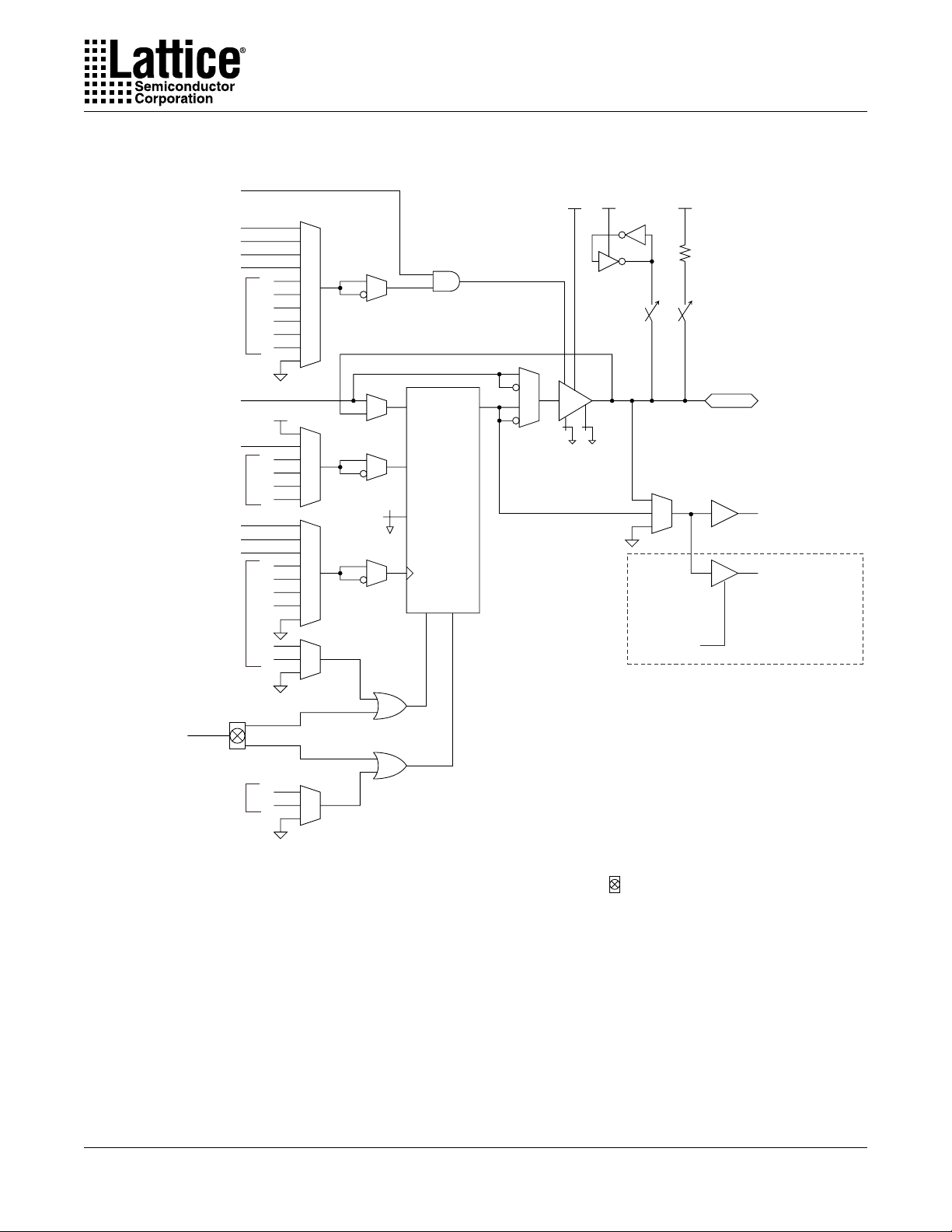
Figure 4. ispLSI 8000 I/O Cell
Specifications ispLSI 8840
TOE
GLOBAL OE0
GLOBAL OE1
GLOBAL OE2
GLOBAL OE3
From Output
Control Bus
Multiplexed Output From
Big Fast Megablock or
Global Track
GLOBAL I/O CLOCK ENABLE
From Output
Control Bus
GLOBAL I/O CLOCK0
GLOBAL I/O CLOCK1
QUADRANT I/O CLOCK
From Output
Control Bus
DQ
CLKEN
R/L
R
P
VCCIO
Slew
Rate
VCCIO
Open
Drain
VCCIO
Big Fast Megablock I/O Pad
or Global I/O Pad
To Specific
Big Fast Megablock
or Global Tracks
To Specific
Global Tristate Bus
From Output
Control Bus
Global I/O Cell
Only
GRST
From Output
Control Bus
: Function Selector (E2 Cell Controlled)
7
Page 8

Specifications ispLSI 8840
Output Control Organization
The Global OE signals and Test OE signal are driven
from the dedicated external control input pins.
In addition to the data input and output to the I/O cells,
each I/O cell can have up to six different I/O cell control
signals. In addition to the internal OE control, the five
control signals for each I/O cell consist of pin OE control,
clock enable, clock input, asynchronous preset and asynchronous reset. All of the I/O control signals can be driven
either from the dedicated external input pins or from the
internal control bus.
The output enable of each I/O cell can be driven by 21
different sources – 16 from the output control bus, four
from the Global OE pins and one from the Test OE pin.
The 16-bit wide output control buses are organized in four
different quadrants as shown in Figure 5. Since each
GLB is capable of generating the output control signals,
each of the output control bus signals can be driven from
a unique GLB. The 42 GLBs can generate a total of 42
unique I/O control signals. Referring to Figure 2, the GLB
generates its output control signal from control product
term (PT81).
Figure 5 also illustrates how the quadrant clocks are
routed to the appropriate quadrant I/O cells.
Figure 5. Output Control Bus and Quadrant Organization
Q
ra
, 1
d
a
t 0
u
n
B
(I/O
id
-B
it W
6
-B
0
O
e
<
6
-1
0
>
1
, Q
tp
u
t C
u
o
K
L
C
IO
s
u
l B
tro
n
)
0
s
u
l B
o
tr
n
o
t C
u
tp
u
O
e
id
it W
-B
6
, 1
t 1
n
ra
d
a
u
Q
)
1
K
L
C
IO
, Q
>
3
-2
2
1
<
5
-G
0
G
(I/O
s
u
G
B
L
G
ra
e
n
e
te
d
O
tp
u
t
u
tro
n
o
C
(se
F
e
ig
u
Q
d
a
u
ra
n
(I/O
t 2
6
, 1
B
-B
0
ro
F
m
1
8
P
l
re
2
)
-B
it W
<
6
2
1
T
id
tp
u
O
e
t C
u
o
-2
3
L
, Q
>
C
IO
s
u
l B
tro
n
)
2
K
l B
tro
n
o
t C
u
tp
u
O
e
id
it W
-B
6
, 1
t 3
n
a
r
d
a
u
Q
OE Bus.eps
)
3
K
L
C
IO
, Q
>
1
1
-
0
<
5
-G
0
G
(I/O
8
Page 9

Figure 6. Boundary Scan Register Circuit for I/O Pins
SCANIN
(from previous
cell)
BSCAN
Registers
DQ DQ
PROG_MODE
BSCAN
Latches
Specifications ispLSI 8840
HIGHZ
EXTEST
TOE
Normal
Function
EXTEST
PROG_MODE
OE
0
1
DQ
DQ
Shift DR
*Internal power-up reset signal. Not connected to external reset pin.
Clock DR
Update DR
DQ
Reset*
Figure 7. Boundary Scan Register Circuit for Input-Only Pins
Normal
Function
0
1
SCANOUT
(to next cell)
I/O Pin
Input Pin
SCANIN
(from previous
cell
Shift DR
Clock DR
DQ
9
SCANOUT
(to next cell)
Page 10

Specifications ispLSI 8840
Figure 8. Boundary Scan Waveforms and Timing Specifications
TMS
TDI
T
btsu
T
btch
TCK
TDO
Data to be
captured
Data to be
driven out
SYMBOL
t
btcp TCK Clock Pulse Width 400 µs
t
btch
t
btcl
t
btsu
t
bth
t
rf TCK, TDI, TMS Rise and Fall Time — mV/ns
t
btco
t
btoz TAP Controller, TCK to TDO High-Impedance 25 ns—
t
btvo
t
btcsu
t
btch
t
btuco
t
btuoz
t
btuov
TCK Pulse Width High
TCK Pulse Width Low
TDI, TMS Setup Time to TCK
TDI, TMS Hold Time from TCK
TAP Controller, TCK to TDO Valid
TAP Controller, TCK to TDO High-Impedance to Valid Output
BSCAN Test Capture Register Setup Time
BSCAN Test Capture Register Hold Time
BSCAN Test Update Register Clock to Valid Output
BSCAN Test Update Register Clock to High-Impedance
BSCAN Test Update Register High-Impedance to Valid Output
T
btcl
T
btvo
T
btcsu
T
btuov
PARAMETER
Data Captured
T
bth
T
btcp
T
btco
Valid Data Valid Data
T
btch
T
btuco
Valid Data Valid Data
MIN
0.1
0.05
0.05
25
25
50
—
—
20
25
—
—
—
T
btoz
T
btuoz
MAX UNITS
200 µs
200
—
25 ns
25
—
25
25
µs
ns
ns—
ns
ns
ns—
ns
ns
ns25
Table 2-0010/8840
10
Page 11

Specifications ispLSI 8840
Absolute Maximum Ratings
1,2
Supply Voltage Vcc.................................. -0.5 to +7.0V
Input Voltage Applied........................-2.5 to VCC +1.0V
Tri-Stated Output Voltage Applied.... -2.5 to VCC +1.0V
Storage Temperature................................ -65 to 150°C
Case Temp. with Power Applied .............. -55 to 125°C
Max. Junction Temp. (TJ) with Power Applied ... 140°C
1. Stresses above those listed under the “Absolute Maximum Ratings” may cause permanent damage to the device. Functional
operation of the device at these or at any other conditions above those indicated in the operational sections of this specification
is not implied (while programming, follow the programming specifications).
2. Compliance with the Thermal Management section of the Lattice Semiconductor Data Book or CD-ROM is a requirement.
DC Recommended Operating Condition
MIN. MAX. UNITS
3.0
2.0
0.0
5.25
V +1
CC
0.8
V
V
V
Table 2-0005/8840
V
V
V
V
V
V
SYMBOL
CC
CCIO
IH
IL
OH
OL
PARAMETER
Supply Voltage Commercial T = 0°C to 70°C 4.75 5.25 V
Output Supply Voltage
Input High Voltage
Input Low Voltage
Output High Voltage 2.4 — V
Output Low Voltage — 0.4 V
A
Capacitance (TA=25°C,f=1.0 MHz)
SYMBOL
C
1
C
2
C
3
I/O Capacitance
Clock Capacitance
Global Input Capacitance
PARAMETER
Erase/Reprogram Specification
PARAMETER MINIMUM MAXIMUM UNITS
ispLSI Erase/Reprogram Cycles
UNITSTYPICAL TEST CONDITIONS
10
10
10
10000 – Cycles
pf V = 5.0V, V = 2.0V
pf V = 5.0V, V = 2.0V
pf V = 5.0V, V = 2.0V
CC I/O
CC CK
CC G
Table 2-0006/8840
Table 2-0008/3320
11
Page 12

Switching Test Conditions
+ 5V
R
1
(VCC and V
CCIO
)
R
2
C
L
*
Device
Output
Test
Point
*
CL includes Test Fixture and Probe Capacitance.
0213A/8840
2
3
4
Specifications ispLSI 8840
Input Pulse Levels
Input Rise and Fall Time
Input Timing Reference Levels
Ouput Timing Reference Levels
Output Load
3-state levels are measured 0.5V from
GND to 3.0V
≤ 1.5 ns 10% to 90%
1.5V
1.5V
See Figure 2
Table 2-0003/8840
Figure 9. Test Load
steady-state active level.
Output Load Conditions (See Figure 9)
TEST CONDITION R1 R2 CL
A 470Ω 390Ω 35pF
∞
∞
390Ω 35pF
390Ω 5pF
Table 2-0004A/8840
Active High
B
Active Low
Active High to Z
at V -0.5V
C
Active Low to Z
at V +0.5V
OH
OL
470Ω 390Ω 35pF
470Ω 390Ω 5pF
DC Electrical Characteristics
Over Recommended Operating Conditions
SYMBOL
V
OL
V
OH
I
IL
Output Low Voltage
Output High Voltage
Input or I/O Low Leakage Current
PARAMETER
I = 8 mA
OL
I = -4 mA
OH
0.0V ≤ V ≤ 0.8V
3.5V ≤ V ≤ V
V = 5V
CCIO
(V - 0.2) ≤ V ≤ V
I
IH
I
PU
I
BHL
I
BHH
I
BHLO
I
BHHO
V
BHT
I
OS
I
CC
1. One output at a time for a maximum duration of one second. V = 0.5V was selected to avoid test problems
Input or I/O High Leakage Current
Active Pullup Current, Input or I/O
Bus-Hold Low Sustaining Current V = 0.8V
Bus-Hold High Sustaining Current -50 ––µA
Bus-Hold Low, Overdrive Current ––550 µA
Bus-Hold High, Overdrive Current ––-550 µA
Bus-Hold Trip Point (1.4V Nominal) 0.8 – 2.0 V
1
Output Short Circuit Current
2,4
Operating Power Supply Current
CCIO
V = 3.3V
CCIO
V < V ≤ 5.25V
CCIO
V >V
IN
CCIO
0V ≤ V ≤ 2.0V
IN
IN
V = 2.0V
IN
0V ≤ V ≤ V
IN CCIO
0V ≤ V ≤ V
IN CCIO
V = 5V, V
CC OUT
V = 0.0V, V = 3.0V High Speed Mode
IL IH
f = 1MHz Low Power Mode
CLOCK
CONDITION MIN. TYP. MAX. UNITS
–
2.4
IN
IN CC
IN
IN CCIO
–
–
––10 µA
––10 µA
-10
50 ––µA
= 0.5V
––-200 mA
– 630 – mA
– 340 – mA
OUT
by tester ground degradation. Characterized but not 100% tested.
. Measured using 42 20-bit counters.
. Typical values are at V = 5V and T = 25°C.
. Maximum I varies widely with specific device configuration and operating frequency.
CC
CC
A
3
–
–
–
–
–
0.4
–
-10
10
-250
Table 2-0007/8840
V
V
µA
µA
µA
12
Page 13

Specifications ispLSI 8840
External Switching Characteristics
1
Over Recommended Operating Conditions
PARA-
METER
t
pd1
t
pd2
f
max
t
suq
t
hq
t
coq
t
sug
t
hg
t
cog
t
su1
t
h1
t
co1
t
suceq
t
hceq
t
suceg
t
hceg
t
goe
t
rglb
t
rio
t
rw
t
wh
t
wl
1. Unless noted otherwise, all parameters use PTSA and CLK0.
2. Refer to Timing Model in this data sheet for further details.
3. Standard 20-bit counter with local feedback.
4. Refer to Switching Test Conditions section.
TEST
COND.
A
A
–
–
–
A
–
–
A
–
–
A
–
–
–
–
B/C
–
–
–
–
–
2
4
Prop Delay, BFM Input to Same BFM Output, 4 PT Bypass – 10.0 ns
1
Prop Delay, Global Input to Global Output – ns
2
Clk Frequency, Local Feedback, Same GLB 90.0 –
3
I/O Cell Reg, Data Setup Time, Quadrant I/O Clock 8.0 – ns
4
I/O Cell Reg, Data Hold Time, Quadrant I/O Clock – ns
5
I/O Cell Reg, Quadrant Clock to Output Delay 6.0 ns
6
I/O Cell Reg, Data Setup Time, Global I/O Clock – ns
7
I/O Cell Reg, Data Hold Time, Global I/O Clock – ns
8
I/O Cell Reg, Global Clock to Output Delay 7.5 ns
9
GLB Reg Setup, BFM Input to Same BFM GLB, 4 PT Bypass – ns
10
GLB Reg Hold Time, BFM Input to Same BFM GLB 0.0 ns
11
GLB Reg, Global Clock to Same BFM Output Delay 10.0 ns
12
I/O Cell Reg, CLKEN Setup Time, Quadrant I/O Clock 6.5 ns
13
I/O Cell Reg, CLKEN Hold Time, Quadrant I/O Clock 0.0 ns
14
GLB Reg, CLKEN Setup Time, Global Clock 4.5 ns
15
GLB Reg, CLKEN Hold Time, Global Clock 0.0 ns
16
Global Output Enable/Disable Delay – ns
17
Global Reset/Preset Time, GLB Reg – 15.0 ns
18
Global Reset/Preset Time, I/O Cell Reg – 10.0 ns
19
Global Reset/Preset Pulse Duration 6.5 – ns
20
Global or Quadrant Clock Pulse, High Duration 6.0 – ns
21
Global or Quadrant Clock Pulse, Low Duration 6.0 – ns
22
DESCRIPTION#
-110
MIN. MAX.
– 8.5
–
3
110
0.0
6.0
0.0
4.5
–
4.5
6.0
–
5.0
0.0
–
8.0
5.0
0.0
3.5
0.0
8.0
–
– 12.0
– 8.0
5.0 –
4.0 –
4.0 –
–
–
–
–
–
–
–
–
–
–
-90 -60
MIN. MAX.
16.013.5
0.0
–
6.0
0.0
–
7.0
–
–
–
–
–
–
10.0
UNITS
MAX.
MIN.
– 15.0
–
24.0
60.0 – MHz
12.0 –
–
0.0
9.0
–
–
9.0
0.0
–
11.0
–
0.0
–
15.0
9.5
0.0
6.5
0.0
15.0
–
– 22.0
– 15.0
9.5 –
9.0 –
9.0 –
–
–
–
–
–
–
Table 2-0030/8840
10.0
13
Page 14

Specifications ispLSI 8840
Internal Timing Parameters
Over Recommended Operating Conditions
PARAMETER #
I/O Cell Delay
2
DESCRIPTION
tidcom 23 Input Pad and Input Buffer, Combinatorial Input – 0.1 – 0.1 – 0.2 ns
tidreg 24 Input Pad and Input Buffer, Registered Input – 8.0 – 9.4 – 13.9 ns
tobp 25 Output Register/Latch Bypass to Output Buffer – 0.0 – 0.0 – 0.0 ns
tibp 26 Input Register/Latch Bypass to BFM Routing or GRP – 0.2 – 0.2 – 0.4 ns
tiolat 27 I/O Cell Latch, Transparent Mode – 2.0 – 2.4 – 3.6 ns
tioco 28 I/O Cell Register/Latch, Clk/Gate to Output – 1.0 – 1.2 – 2.0 ns
tiosu 29 I/O Cell Register/Latch, Setup Time 0.4 – 0.7 – 1.4 – ns
tioh 30 I/O Cell Register/Latch, Hold Time 4.1 – 4.4 – 6.9 – ns
tiorst 31 I/O Cell Register/Latch, Reset or Set Time – 2.3 – 2.9 – 4.4 ns
tiosuce 32 I/O Cel l R e g i ster/Latch, Setup Time for Clk Enable 2.6 – 2.7 – 3.8 – ns
tiohce 33 I/O c e l l R e g ister/Latch, Hold Time for Clk Enable 1.9 – 1.9 – 2.9 – ns
todreg 34 I/O Cell Output Buffer Delay, Registered Output – 1.1 – 1.3 – 1.9 ns
todcom 35 I/O C e l l O utput Buffer Delay, Combinatorial Output – 1.7 – 2.0 – 3.0 ns
todz 36 Output Driver Disable Time – 2.0 – 2.3 – 3.5 ns
tslf 37 Slew Rate Adder, Fast Slew Rate – 0.0 – 0.0 – 0.0 ns
tsls 38 Slew Rate Adder, Slow Slew Rate – 5.0 – 5.0 – 7.5 ns
GLB / Macrocell Delay
tandhs 39 AND Array, High Speed Mode – 3.6 – 4.2 – 6.4 ns
tandlp 40 AND Array, Low Power Mode – 7.1 – 8.4 – 12.6 ns
t1pt 41 Single Product Term Bypass – 3.6 – 4.3 – 6.2 ns
t4ptcom 42 Four Product Term Bypass, Combinatorial Macrocell – 0.2 – 0.3 – 0.4 ns
t4ptreg 43 Four Product Term Bypass, Registered Macrocell – 3.4 – 4.4 – 6.1 ns
tptsa 44 Product Term Sharing Array – 3.7 – 4.5 – 6.8 ns
tmbp 45 Macrocell Register/Latch Bypass – 0.0 – 0.0 – 0.0 ns
tmlat 46 Macrocell Latch, Transparent Mode – 0.2 – 0.3 – 0.9 ns
tmco 47 Macrocell Register/Latch, Clk/Gate to Output – 0.2 – 0.3 – 0.5 ns
tmsu 48 Macrocell Register/Latch, Setup Time 0.4 – 0.8 – 1.2 – ns
tmh 49 Macrocell Register/Latch, Hold Time 3.8 – 4.5 – 6.1 – ns
tmrst 50 Macrocell Register/Latch, Reset or Set Time – 4.0 – 5.2 – 7.3 ns
tmsuce 51 Macrocell Register/Latch, Setup Time for Clk Enable 1.7 – 1.8 – 2.4 – ns
tmhce 52 Macrocell Register/Latch, Hold Time for Clk Enable 1.0 – 0.9 – 1.3 – ns
tftog 53 Toggle Flip-Flop Feedback – 3.9 – 4.7 – 6.8 ns
tfloc 54 Local Feedback to AND Array – 1.1 – 1.3 – 1.9 ns
tpck 55 Single Product Term, Clk 1.0 2.5 1.5 3.5 2.3 5.3 ns
tpcken 56 Single Product Term, Clk Enable – 2.6 – 3.1 – 4.6 ns
tsck 57 Shared Product Term, Clk 1.6 2.4 1.8 2.5 2.7 3.8 ns
tscken 58 Shared Product Term, Clk Enable – 2.4 – 2.5 – 3.8 ns
tprst 59 Single Product Term, Reset or Set Delay – 1.7 – 2.0 – 3.0 ns
trdir 60 Macrocell Register, Direct Input from GRP – 1.8 – 2.1 – 2.7 ns
-110 -90 -60
MIN MAX MIN MAX MIN MAX UNITS
14
Page 15

Internal Timing Parameters
Over Recommended Operating Conditions
Specifications ispLSI 8840
PARAMETER #
BFM / Global Routing Pool Delay
2
DESCRIPTION
-110 -90 -60
MIN MAX MIN MAX MIN MAX UNITS
tbfmi 61 BFM Routing Delay, Signal from I/O Cell – 0.2 – 0.3 – 0.4 ns
tgrpi 62 GRP Delay, Signal from I/O Cell – 0.2 – 0.2 – 0.4 ns
tgrpiz 63 Internal Tristate Bus Enable/Disable, I/O Cell Buffer – 2.2 – 2.5 – 3.8 ns
tbfmm 64 BFM Routing Delay, Signal from Macrocell – 1.9 – 2.3 – 3.4 ns
tgrpm 65 GRP Delay, Signal from Macrocell – 2 – 2.4 – 3.5 ns
tgrpmz 66
Internal Tristate Bus Enable/Disable, Macrocell Buffer
– 4 – 4.7 – 7.1 ns
tbfmg 67 BFM Routing Delay, Signal from GRP – 1.6 – 1.8 – 2.8 ns
tgrpb 68 GRP Delay, Signal from BFM Routing – 2.5 – 3.0 – 4.4 ns
tbcom 69 BFM Routing to I/O Cell, Combinatorial Path – 0.5 – 0.6 – 0.8 ns
tbreg 70 BFM Routing to I/O Cell, Registered Path – 3.5 – 4.1 – 6.1 ns
tgcom 71 GRP to I/O Cell, Combinatorial Path – 0.4 – 0.4 – 0.6 ns
tgreg 72 GRP to I/O Cell, Registered Path – 3.4 – 3.9 – 5.9 ns
I/O Control Bus Delay
tpiock 73 Product Term as I/O Cell Register Clock – 6.5 – 7.7 – 11.6 ns
tpiocken 74 Product Term as I/O Cell Register Clock Enable – 6.5 – 7.7 – 11.6 ns
tpoe 75 Product Term as Output Buffer Enable/Disable – 6.7 – 7.9 – 11.9 ns
tpiorst 76
Product Term as I/O Cell Register Reset or Set Delay
– 7.3 – 8.8 – 13.2 ns
tpioz 77 Internal Tristate Bus Control Signal for I/O Cell Buffer – 6.0 – 7.1 – 10.7 ns
Global Control Delay
tgck 78 Global Macrocell Register Clk 2.9 3.7 3.1 4.9 4.6 7.3 ns
tgcken 79 Global Macrocell Register Clk Enable 4.7 4.7 5.8 5.8 8.7 8.7 ns
tgiock 80 Global I/O Register Clk 3.9 3.9 4.1 5.0 6.2 7.0 ns
tgiocken 81 Global I/O Register Clk Enable 4.8 4.8 5.9 5.9 8.9 8.9 ns
tqck 82 Quadrant I/O Register Clk 2.4 2.4 2.1 3.5 3.2 5.1 ns
tgoe 83 Global Output Enable – 6 – 7.7 – 11.5 ns
ttoe 84 Test Output Enable – 7.3 – 8.6 – 12.9 ns
tgmrst 85 Global GLB Register Reset – 4 – 5.1 – 7.6 ns
tgiorst 86 Global I/O Cell Register Reset – 4.6 – 5.9 – 8.8 ns
1. Internal Timing Parameters are not tested and are for reference only.
2. Refer to Timing Model in this data sheet for further details.
15
Page 16

ispLSI 8840 Timing Model
Input Buffer and I/O Cell Register
I/O register delays
t
#25,
obp
#26,
t
ibp
#27,
I/O
pad
Input
pad
Input buffer
delays
t#23,
idcom
t#24,
idreg
Global control
delay
t
#78,
gck
#79,
t
gcken
t
#80,
giock
#81,
t
giocken
#82,
t
qck
#83,
t
goe
t#84,
toe
#85,
t
gmrst
#86,
t
giorst
#28,
#29,
#30,
#32,
#33,
t
iolat
t
ioco
t
iosu
t
ioh
t#31,
iorst
t
iosuce
t
iohce
Output path
Input path
BFM Routing Pool
GLB/
Macrocell
AND array
#39,
t
andhs
#40,
t
andlp
t#61,
bfmi
t#64,
bfmm
Local feedback
t#54,
floc
PTSA
#41,
t
1pt
#42,
t
4ptcom
#43,
t
4ptreg
t
#44,
ptsa
PT Mcell controls
t
#55,
pck
#56,
t
pcken
t
#57,
sck
t
#58,
scken
t
#59,
prst
PT I/O control bus
#73,
t
piock
#74,
t
piocken
#75,
t
poe
#76,
t
piorst
t
#77,
pioz
t#67,
bfmg
Toggle feedback
#53,
Mcell register
t
ftog
#45,
#46,
#47,
#48,
#49,
#50,
#51,
#52,
Specifications ispLSI 8840
#69,
t
mbp
t
mlat
t
mco
t
msu
t
mh
t
mrst
t
msuce
t
mbce
#70,
#71,
#72,
t
bcom
t
breg
t
gcom
t
greg
Bus direct
Output routing
t#60,
rdir
z
Global
Routing
Plane
#62,
t
grpi
#63,
t
grpiz
#65,
t
grpm
#66,
t
grpmz
t
#68,
grpb
Output
buffer
delays
t
#34,
odreg
t
#35,
odcom
t
#36,
odz
8K_Model.eps
Output
slew rate
adders
#37,
t
slf
t
#38,
sls
I/O
pad
16
Page 17

Example Timing Calculations
Specifications ispLSI 8840
tpd1 = (BFM Input Path Delay) + (GLB Delay) + (Output Path Delay)
tidcom + tibp + tbfmi) + (tandhs + t4ptcom + tmbp) + (tbfmm + tbcom + tobp + todcom + tslf)
= (
= (#23 + #26 + #61) + (#39 + #42 + #45) + (#64 + #69 + #25 + #35 + #37)
= (0.1 + 0.2 + 0.2) + (3.6 + 0.2 + 0.0) + (1.9 + 0.5 + 0.0 + 1.7 + 0.0)
= 8.4 ns
tpd (within BFM)
= (BFM Delay) + (GLB Delay)
tbfmm) + (tandhs + t4ptcom + tmbp)
= (
= (#64) + (#39 + #42 + #45)
= (1.9) + (3.6 + 0.2 + 0.0)
= 5.7 ns
tpd (between BFMs)
= (GRP Delay) + (BFM Delay) + (GLB Delay)
tgrpm) + (tbfmg) + (tandhs + t4ptcom + tmbp)
= (
= (#65) + (#67) + (#39 + #42 + #45)
= (2.0) + (1.6) + (3.6 + 0.2 + 0.0)
= 7.4 ns
BFM I/O to internal tri-state Enable/Disable
= (BFM Input Path Delay) + (GLB Delay, 1PT) + (Tri-state Control Delay)
tidcom + tibp + tbfmi) + (tandhs + t1pt + tmbp) + (tgrpmz)
= (
= (#23 + #26 + #61) + (#39 + #41 + #45) + (#66)
= (0.1 + 0.2 + 0.2) + (3.6 + 3.6 + 0.0) + (4.0)
= 11.7 ns
tsu1 = (BFM Input Path Delay) + (GLB Setup Time) - (Min. Global Clock Delay)
tidcom + tibp + tbfmi) + (tandhs + t4ptreg + tmsu) – (tgck min)
= (
= (#23 + #26 + #61) + (#39 + #43 + #48) – (#78)
= (0.1 + 0.2 + 0.2) + (3.6 + 3.4 + 0.4) – (2.9)
= 5 ns
Fmax = (Global Clk to MC Output) + (Local Feedback) + (GLB Setup Time)
1/
tmco) + (tfloc) + (tandhs + tptsa + tmsu)
= (
= (#47) + (#54) + (#39 + #44 + #48)
= (0.2) + (1.1) + (3.6 + 3.7 + 0.4)
= 9 ns
Fmax = 111 MHz
Note: Calculations are based upon timing specifications for the ispLSI 8840-110L
17
Page 18

Power Consumption
Specifications ispLSI 8840
Power consumption in the ispLSI 8840 device depends
on two primary factors: the speed at which the device is
operating and the number of product terms used. The
product terms have a fuse-selectable speed/power
tradeoff setting. Each group of four product terms has a
single speed/power tradeoff control fuse that acts on the
complete group of four. The fast “high-speed” setting
Figure 10. Typical Device Power Consumption vs fmax
1200
1100
1000
900
800
700
CC (mA)
I
600
500
400
operates product terms at their normal full power consumption. For portions of the logic that can tolerate
longer propagation delays, selecting the slower “lowpower” setting will significantly reduce the power
dissipation for these product terms. Figure 10 shows the
relationship between power and operating speed.
ispLSI 8840
Turbo
Non-Turbo
300
200
0 102030405060708090100
f
max (MHz)
Notes: Configuration of 42 20-bit counters
Typical current at 5V, 25° C
ICC can be estimated for the ispLSI 8840 using the following equation:
ICC = 48.0 + (# of Turbo PTs * 0.346) + (# of Non-Turbo PTs * 0.165) + (# of Macrocells Used * fmax * AF * 0.049)
# of Turbo PTs = Number of Turbo Product Terms Used in Design
# of Non-Turbo PTs = Number of Non-Turbo Product Terms Used in Design
fmax = Maximum Operating Frequency
AF (Activity Factor) =
Note: An Activity Factor of 1.0 means all macrocell registers toggle at Fmax. An Activity Factor of 0.5 means the
average macrocell registers toggle at half of fmax.
The I
on average exists. These values are for estimates only. Since the value of I
and the program in the device, the actual I
estimate is based on typical conditions (VCC = 5.0V, room temperature) and an assumption of two GLB loads
CC
Average Macrocell Toggle Frequency
Fmax
should be verified.
CC
is sensitive to operating conditions
CC
110 120
0127/8840
18
Page 19

Specifications ispLSI 8840
Signal Descriptions
Signal Name Description
CLK0, CLK1, Dedicated clock input for the GLB registers only. These clock inputs are connected to one of the clock
CLK2 inputs of all GLB registers in the device.
CLKEN Dedicated clock enable input for the GLB registers only. This input is available as a clock enable for
each GLB register in the device. Use of the clock enable input eliminates the need for the user to gate
the clock to the register.
GIOCLK0, Dedicated clock inputs for the I/O registers only. These clock inputs are connected to one of the clock
GIOCLK1 inputs of all I/O registers in the device.
GND Ground (GND)
GOE Global Output Enable inputs.
SET/RESET Dedicated reset/preset pin connected to ALL registers in the device, GLB registers and
I/O registers. Each register can independently choose to be reset or preset when this signal goes
active. The active polarity is user-selectable.
IOCLKEN Dedicated clock enable input for the I/O registers only. This input is available as a clock enable input for
all I/O registers in the device. Use of the clock enable input eliminates the need for the user to tie the
clock to the I/O register.
I/O Input/Output – These are the general purpose I/O used by the logic array.
BSCAN/ispEN Input – Dedicated in-system programming enable input. When this is high, the BSCAN TAP
controller signals TMS, TDI, TDO and TCK are enabled. When this is brought low, the ISP State
Machine control signals MODE, SDI, SDO and SLCK are enabled. High-to-low transition will put the
device in the Lattice ISP programming mode and put all I/O in the high-Z state.
TMS/MODE Input – This signal performs two functions. It is the Test Mode Select input signal when ispEN is logic
high. When ispEN is logic low, it controls the operation of the ISP State Machine.
1
NC
QIOCLK0 Dedicated clock inputs for the I/O registers only. These clock inputs are connected to the I/O registers
QIOCLK1 on the same side of the device only, they are not connected to all of the I/O registers. Use of these
QIOCLK2 quadrant I/O clocks gives the fastest tco from the device.
QIOCLK3
TCK/SCLK Input – This signal performs two functions. It is the Test Clock input signal when ispEN is logic high.
TDI/SDI Input – This signal performs two functions. It is the Test Data input signal when ispEN is logic high.
TDO/SDO Output – This signal performs two functions. When ispEN is logic low, it reads the ISP data. When
TOE Test Output Enable pin – This pin tristates all I/O pins when a logic low is driven.
VCC Vcc
VCCIO Power supply for the output drivers. The internal logic of the device is connected to VCC which is
1. NC pins are not to be connected to any active signals, VCC or GND.
No connect.
When ispEN is logic low, it functions as a clock signal for the Serial Shift Register.
When ispEN is logic low, it functions as an input to load programming data into the device. SDI is also
used as one of the two control signals for the ISP State Machine.
ispEN is high, it functions as Test Data Out.
always 5V. The output drivers are connected to VCCIO which can be equal to VCC or 3.3V. This allows
the output drivers to be powered from 3.3V, for example, to interface directly with another 3.3V device.
19
Page 20

Specifications ispLSI 8840
Signal Locations (432-Ball BGA Package)
Signal 432-Ball BGA
CLK0, CLK1, CLK2 A18, P29, AL19
CLKEN C18
GIOCLK0, A19, AJ18
GIOCLK1
GND A1, A2, A16, A30, A31, B1, B5, B9, B13, B19, B23, B27, B31, E2, E30, J2, J30, N2, N30, T1, T31, W2,
W30, AC2, AC30, AG2, AG30, AK1, AK5, AK9, AK13, AK19, AK23, AK27, AK31, AL1, AL2, AL16,
AL30, AL31
GOE0, GOE1 D18, T29, AH18, T2
GOE2, GOE3
SET/RESET P1
IOCLKEN AL20
BSCAN/ispEN AG28
TMS/MODE E4
1
NC
QIOCLK0, D17, R31, AL18, T3
QIOCLK1,
QIOCLK2,
QIOCKK3
TCK/SCLK AH2
TDI/SDI E3
TDO/SDO AH3
TOE V3
VCC A3, A10, A22, A29, B14, B18, C1, C31, K1, K31, P2, P30, V2, V30, AB1, AB31, AJ1, AJ31, AK14,
VCCIO D5, D9, D12, D15, D20, D23, D27, H4, H28, M4, M28, T4, T28, Y4, Y28, AE4, AE28, AH5, AH9, AH12,
1. NC pins are not to be connected to any active signals, VCC or GND.
A4, B30, D1, D31, AH1, AH31, AK2, AK30, AL4, AL28
AK18, AL3, AL10, AL22, AL29
AH15, AH20, AH23, AH27
20
Page 21

Specifications ispLSI 8840
I/O Pin Locations (432-Ball BGA Package)
Signal BGA Signal BGA Signal BGA Signal BGA Signal BGA
I/O G0 <0> C2
I/O G0 <1> F4
I/O G0 <2> F3
I/O G0 <3> D2
I/O G0 <4> G4
I/O G0 <5> F2
I/O G0 <6> G3
I/O G0 <7> E1
I/O G0 <8> G2
I/O G0 <9> H3
I/O G0 <10> F1
I/O G0 <11> J4
I/O G0 <12> F31
I/O G0 <13> G30
I/O G0 <14> H29
I/O G0 <15> F30
I/O G0 <16> E31
I/O G0 <17> G29
I/O G0 <18> G28
I/O G0 <19> F29
I/O G0 <20> E29
I/O G0 <21> F28
I/O G0 <22> D30
I/O G0 <23> E28
I/O G1 <0> L1
I/O G1 <1> L2
I/O G1 <2> L3
I/O G1 <3> L4
I/O G1 <4> K2
I/O G1 <5> J1
I/O G1 <6> K3
I/O G1 <7> K4
I/O G1 <8> H1
I/O G1 <9> G1
I/O G1 <10> J3
I/O G1 <11> H2
I/O G1 <12> J28
I/O G1 <13> J29
I/O G1 <14> H30
I/O G1 <15> G31
I/O G1 <16> H31
I/O G1 <17> K28
I/O G1 <18> K29
I/O G1 <19> K30
I/O G1 <20> J31
I/O G1 <21> L28
I/O G1 <22> L29
I/O G1 <23> L30
I/O G2 <0> M3
I/O G2 <1> M2
I/O G2 <2> M1
I/O G2 <3> N4
I/O G2 <4> N3
I/O G2 <5> N1
I/O G2 <6> P3
I/O G2 <7> P4
I/O G2 <8> R2
I/O G2 <9> R3
I/O G2 <10> R4
I/O G2 <11> R1
I/O G2 <12> R30
I/O G2 <13> R29
I/O G2 <14> R28
I/O G2 <15> P31
I/O G2 <16> P28
I/O G2 <17> N31
I/O G2 <18> N29
I/O G2 <19> N28
I/O G2 <20> M31
I/O G2 <21> M30
I/O G2 <22> L31
I/O G2 <23> M29
I/O G3 <0> Y3
I/O G3 <1> Y1
I/O G3 <2> Y2
I/O G3 <3> W4
I/O G3 <4> W3
I/O G3 <5> W1
I/O G3 <6> V1
I/O G3 <7> V4
I/O G3 <8> U1
I/O G3 <9> U4
I/O G3 <10> U3
I/O G3 <11> U2
I/O G3 <12> T30
I/O G3 <13> U28
I/O G3 <14> U29
I/O G3 <15> U30
I/O G3 <16> U31
I/O G3 <17> V28
I/O G3 <18> V29
I/O G3 <19> V31
I/O G3 <20> W29
I/O G3 <21> W28
I/O G3 <22> W31
I/O G3 <23> Y31
I/O G4 <0> AA2
I/O G4 <1> AA3
I/O G4 <2> AA4
I/O G4 <3> AA1
I/O G4 <4> AB3
I/O G4 <5> AB4
I/O G4 <6> AB2
I/O G4 <7> AC3
I/O G4 <8> AC4
I/O G4 <9> AC1
I/O G4 <10> AD2
I/O G4 <11> AD3
I/O G4 <12> AC28
I/O G4 <13> AC29
I/O G4 <14> AC31
I/O G4 <15> AB28
I/O G4 <16> AB29
I/O G4 <17> AB30
I/O G4 <18> AA29
I/O G4 <19> AA28
I/O G4 <20> AA30
I/O G4 <21> AA31
I/O G4 <22> Y30
I/O G4 <23> Y29
I/O G5 <0> AG4
I/O G5 <1> AG3
I/O G5 <2> AG1
I/O G5 <3> AF1
I/O G5 <4> AF4
I/O G5 <5> AF3
I/O G5 <6> AF2
I/O G5 <7> AE1
I/O G5 <8> AE3
I/O G5 <9> AE2
I/O G5 <10> AD1
I/O G5 <11> AD4
I/O G5 <12> AD31
I/O G5 <13> AD29
I/O G5 <14> AD28
I/O G5 <15> AD30
I/O G5 <16> AE29
I/O G5 <17> AE30
I/O G5 <18> AE31
I/O G5 <19> AF31
I/O G5 <20> AF28
I/O G5 <21> AF29
I/O G5 <22> AF30
I/O G5 <23> AG31
I/O B0 <0> D3
I/O B0 <1> D4
I/O B0 <2> B2
I/O B0 <3> C3
I/O B0 <4> C4
I/O B0 <5> C5
I/O B0 <6> D6
I/O B0 <7> C6
I/O B0 <8> B3
I/O B0 <9> D7
I/O B0 <10> B4
I/O B0 <11> B6
I/O B0 <12> AJ7
I/O B0 <13> AK6
I/O B0 <14> AH7
I/O B0 <15> AJ6
I/O B0 <16> AK4
I/O B0 <17> AH6
I/O B0 <18> AJ5
I/O B0 <19> AK3
I/O B0 <20> AJ4
I/O B0 <21> AJ3
I/O B0 <22> AH4
I/O B0 <23> AJ2
I/O B1 <0> D8
I/O B1 <1> C7
I/O B1 <2> A5
I/O B1 <3> C8
I/O B1 <4> B7
I/O B1 <5> A6
I/O B1 <6> C9
I/O B1 <7> A7
I/O B1 <8> D10
I/O B1 <9> B8
I/O B1 <10> C10
I/O B1 <11> A8
I/O B1 <12> AH11
I/O B1 <13> AL8
I/O B1 <14> AJ10
I/O B1 <15> AK8
I/O B1 <16> AH10
I/O B1 <17> AL7
I/O B1 <18> AJ9
I/O B1 <19> AK7
I/O B1 <20> AJ8
I/O B1 <21> AL6
I/O B1 <22> AH8
I/O B1 <23> AL5
I/O B2 <0> D11
I/O B2 <1> A9
I/O B2 <2> C11
I/O B2 <3> B10
I/O B2 <4> C12
I/O B2 <5> B11
I/O B2 <6> A11
I/O B2 <7> B12
I/O B2 <8> D13
I/O B2 <9> C13
I/O B2 <10> A12
I/O B2 <11> A13
I/O B2 <12> AJ14
I/O B2 <13> AL13
I/O B2 <14> AJ13
I/O B2 <15> AH13
I/O B2 <16> AL12
I/O B2 <17> AL11
I/O B2 <18> AK12
I/O B2 <19> AJ12
I/O B2 <20> AK11
I/O B2 <21> AK10
I/O B2 <22> AJ11
I/O B2 <23> AL9
I/O B3 <0> D14
I/O B3 <1> C14
I/O B3 <2> A14
I/O B3 <3> C15
I/O B3 <4> B15
I/O B3 <5> A15
I/O B3 <6> B16
I/O B3 <7> C16
I/O B3 <8> D16
I/O B3 <9> A17
I/O B3 <10> B17
I/O B3 <11> C17
I/O B3 <12> AH17
I/O B3 <13> AJ17
I/O B3 <14> AK17
I/O B3 <15> AL17
I/O B3 <16> AH16
I/O B3 <17> AJ16
I/O B3 <18> AK16
I/O B3 <19> AL15
I/O B3 <20> AJ15
I/O B3 <21> AK15
I/O B3 <22> AL14
I/O B3 <23> AH14
I/O B4 <0> A20
I/O B4 <1> B20
I/O B4 <2> C19
I/O B4 <3> A21
I/O B4 <4> D19
I/O B4 <5> C20
I/O B4 <6> B21
I/O B4 <7> A23
I/O B4 <8> C21
I/O B4 <9> B22
I/O B4 <10> A24
I/O B4 <11> D21
I/O B4 <12> AH21
I/O B4 <13> AK24
I/O B4 <14> AL24
I/O B4 <15> AJ21
I/O B4 <16> AK22
I/O B4 <17> AJ20
I/O B4 <18> AL23
I/O B4 <19> AH19
I/O B4 <20> AK21
I/O B4 <21> AJ19
I/O B4 <22> AK20
I/O B4 <23> AL21
I/O B5 <0> A25
I/O B5 <1> C22
I/O B5 <2> B24
I/O B5 <3> D22
I/O B5 <4> B25
I/O B5 <5> C23
I/O B5 <6> A26
I/O B5 <7> C24
I/O B5 <8> B26
I/O B5 <9> D24
I/O B5 <10> C25
I/O B5 <11> A27
I/O B5 <12> AJ26
IO B5 <13> AJ25
I/O B5 <14> AH24
I/O B5 <15> AL27
I/O B5 <16> AK26
I/O B5 <17> AJ24
I/O B5 <18> AJ23
I/O B5 <19> AL26
I/O B5 <20> AH22
I/O B5 <21> AK25
I/O B5 <22> AL25
I/O B5 <23> AJ22
I/O B6 <0> D25
I/O B6 <1> A28
I/O B6 <2> C26
I/O B6 <3> B28
I/O B6 <4> D26
I/O B6 <5> C27
I/O B6 <6> B29
I/O B6 <7> C28
I/O B6 <8> C29
I/O B6 <9> C30
I/O B6 <10> D28
I/O B6 <11> D29
I/O B6 <12> AG29
I/O B6 <13> AH30
I/O B6 <14> AH29
I/O B6 <15> AH28
I/O B6 <16> AJ30
I/O B6 <17> AJ29
I/O B6 <18> AJ28
I/O B6 <19> AH26
I/O B6 <20> AJ27
I/O B6 <21> AK29
I/O B6 <22> AK28
I/O B6 <23> AH25
21
Page 22

Signal Configuration
ispLSI 8840 432-Ball BGA Signal Diagram
31302928272625242322212019181716151413121110987654321
I/O
I/O
I/O
I/O
I/O
I/O
A
B
C
D
E
F
G
H
J
K
L
M
N
P
R
T
U
V
W
Y
AA
AB
AC
AD
AE
AF
AG
AH
AJ
AK
AL
GND GND VCC
I/O
1
NC
QIO
NC
I/O
G0
I/O
G0
I/O
G1
I/O
G1
I/O
G1
I/O
G2
I/O
G2
I/O
G2
I/O
G2
I/O
G3
I/O
G3
I/O
G3
I/O
G3
I/O
G4
I/O
G4
I/O
G5
I/O
G5
I/O
G5
I/O
G5
I/O
B6
<9>
I/O
1
G0
<22>
GND
I/O
G0
<15>
I/O
G0
<13>
I/O
G1
<14>
GND
I/O
G1
<19>
I/O
G1
<23>
I/O
G2
<21>
GND
VCC CLK1
I/O
G2
<12>
I/O
G3
<12>
I/O
G3
<15>
VCC
GND
I/O
G4
<22>
I/O
G4
<20>
I/O
G4
<17>
GND
I/O
G5
<15>
I/O
G5
<17>
I/O
G5
<22>
GND
I/O
1
B6
<13>
I/O
B6
<16>
B6
<6>
I/O
B6
<8>
I/O
B6
<11>
I/O
G0
<20>
I/O
G0
<19>
I/O
G0
<17>
I/O
G0
VCCIO VCCIO
<14>
I/O
G1
<13>
I/O
G1
<18>
I/O
G1
<22>
I/O
G2
VCCIO VCCIO
<23>
I/O
G2
<18>
I/O
G2
<13>
GOE
VCCIO VCCIO
1
I/O
G3
<14>
I/O
G3
<18>
I/O
G3
<20>
I/O
G4
VCCIO VCCIO
<23>
I/O
G4
<18>
I/O
G4
<16>
I/O
G4
<13>
I/O
G5
<13>
I/O
G5
VCCIO VCCIO
<16>
I/O
G5
<21>
I/O
BSCAN
B6
/ ispEN
<12>
I/O
B6
<14>
I/O
B6
<17>
I/O
1
B6
<21>
GND NC
VCC
<16>
<12>
<15>
<16>
<20>
VCC
<22>
<20>
<17>
<15>
CLK1
GND
<16>
<19>
<22>
<23>
<21>
VCC
<14>
<12>
<18>
<19>
<23>
VCC
GND NC
GND GND VCC NC
<1>
I/O
<3>
I/O
<7>
I/O
<10>
I/O
G0
<23>
I/O
G0
<21>
I/O
G0
<18>
I/O
G1
<12>
I/O
G1
<17>
I/O
G1
<21>
I/O
G2
<19>
I/O
G2
<16>
I/O
G2
<14>
I/O
G3
<13>
I/O
G3
<17>
I/O
G3
<21>
I/O
G4
<19>
I/O
G4
<15>
I/O
G4
<12>
I/O
G5
<14>
I/O
G5
<20>
I/O
<15>
I/O
<18>
I/O
<22>
B6
B5
B5
B5
<6>
I/O
B5
<8>
I/O
B6
<2>
I/O
B6
<4>
I/O
B6
<19>
I/O
B5
<12>
I/O
B5
<16>
I/O
B5
<19>
<0>
I/O
B5
<4>
I/O
B5
<10>
I/O
B6
<0>
I/O
B6
<23>
I/O
B5
<13>
I/O
B5
<21>
I/O
B5
<22>
B4
<10>
I/O
B5
<2>
I/O
B5
<7>
I/O
B5
<9>
I/O
B5
<14>
I/O
B5
<17>
I/O
B4
<13>
I/O
B4
<14>
GND
VCCIO
VCCIO
<18>
GND
<18>
<11>
B6
GND
I/O
B6
B6
<5>
B6
VCCIO
B6
VCCIO
I/O
B6
B6
<20>
B6
GND
I/O
1
B5
<15>
<7>
<5>
B4
I/O
B5
I/O
B5
I/O
B4
VCC
I/O
B4
<9>
I/O
B5
<1>
I/O
B5
<3>
I/O
B5
<20>
I/O
B5
<23>
I/O
B4
<16>
VCC
I/O
B4
<3>
I/O
B4
<6>
I/O
B4
<8>
I/O
B4
<11>
I/O
B4
<12>
I/O
B4
<15>
I/O
B4
<20>
I/O
B4
<23>
I/O
<0>
I/O
<1>
I/O
<5>
VCCIO
B4
B4
B4
GIO
CLK0
CLK0
GND VCC
I/O
B4
<2>
I/O
GOE0QIO
B4
<4>
I/O
I/O
B3
GND
B3
<9>
<5>
I/O
I/O
I/O
B3
B3
B3
<4>
<6>
<10>
I/O
I/O
B3
<11>
CLK0
<7>
<8>
B3
I/O
B3
<3>
VCCIO
I/O
B3
CLK
EN
ispLSI 8840
Bottom View
I/O
I/O
GIO
QIO
I/O
B3
B3
<12>
I/O
<13>
I/O
<14>
I/O
<15>
VCCIO
<16>
I/O
I/O
B3
B3
B3
<20>
<17>
I/O
I/O
B3
B3
B3
<21>
<18>
I/O
B3
GND
B3
<19>
2
VCCIO
I/O
B4
<17>
I/O
B4
<22>
IOCLK
EN
GOE
B4
<19>
I/O
B4
CLK1
<21>
GND VCC
CLK2
CLK2
Specifications ispLSI 8840
I/O
I/O
I/O
I/O
I/O
I/O
I/O
I/O
B3
<2>
<11>
VCC GN D
I/O
I/O
B3
<1>
<9>
I/O
I/O
B3
<0>
<8>
I/O
I/O
B3
<23>
<15>
I/O
I/O
B2
<14>
<12>
VCC GN D
I/O
I/O
B3
<13>
<22>
B2
B2
B2
VCC
B2
I/O
B2
<3>
I/O
B1
<10>
I/O
B1
<8>
I/O
B1
<16>
I/O
B1
<14>
I/O
B2
<21>
VCC
<1>
GND
I/O
B1
<6>
VCCIO
VCCIO
I/O
B1
<18>
GND
I/O
B2
<23>
B1
<11>
I/O
B1
<9>
I/O
B1
<3>
I/O
B1
<0>
I/O
B1
<22>
I/O
B1
<20>
I/O
B1
<15>
I/O
B1
<13>
<10>
<6>
I/O
I/O
B2
B2
<5>
<7>
I/O
I/O
B2
B2
B2
<4>
<2>
I/O
B2
B2
VCCIO
<0>
I/O
B2
B1
VCCIO
<12>
I/O
I/O
B2
B2
B2
<22>
<19>
I/O
I/O
B2
B2
<20>
<18>
I/O
I/O
B2
B2
B2
<17>
<16>
<7>
<4>
<1>
<9>
<14>
<12>
<19>
<17>
B1
I/O
B1
I/O
B1
I/O
B0
I/O
B0
I/O
B0
I/O
B1
I/O
B1
B1
<5>
I/O
B0
<11>
I/O
B0
<7>
I/O
B0
<6>
I/O
B0
<17>
I/O
B0
<15>
I/O
B0
<13>
I/O
B1
<21>
VCCIO
VCCIO
I/O
B1
NC1VCC GN D GND
<2>
I/O
GND
B0
<10>
I/O
I/O
B0
B0
<5>
<4>
I/O
B0
<1>
TMS/
MODE
I/O
G0
<1>
I/O
G0
<4>
I/O
G0
<11>
I/O
G1
<7>
I/O
G1
<3>
I/O
G2
<3>
I/O
G2
<7>
I/O
G2
<10>
I/O
G3
<9>
I/O
G3
<7>
I/O
G3
<3>
I/O
G4
<2>
I/O
G4
<5>
I/O
G4
<8>
I/O
G5
<11>
I/O
G5
<4>
I/O
G5
<0>
I/O
B0
<22>
I/O
I/O
B0
B0
<20>
<18>
I/O
GND
B0
<16>
I/O
1
B1
NC
<23>
I/O
I/O
B0
GND
B0
<2>
<8>
I/O
I/O
B0
G0
VCC
<3>
<0>
I/O
I/O
B0
G0
NC
<0>
<3>
TDI/
GND
SDI
<7>
I/O
I/O
G0
G0
<2>
<5>
<10>
I/O
I/O
G0
G0
<9>
<8>
<6>
I/O
I/O
G0
G1
<9>
<11>
<8>
I/O
G1
GND
<10>
<5>
I/O
I/O
G1
G1
VCC
<6>
<4>
I/O
I/O
G1
G1
<2>
<1>
<0>
I/O
I/O
G2
G2
<0>
<1>
<2>
I/O
G2
GND
<4>
<5>
I/O
SET/
G2
VCC
RESET
<6>
I/O
I/O
G2
G2
<11>
<8>
<9>
QIO
GOE
GND
CLK3
3
I/O
I/O
G3
G3
<8>
<11>
<10>
TOE VCC
<6>
I/O
G3
GND
<4>
<5>
I/O
I/O
G3
G3
<1>
<2>
<0>
I/O
I/O
G4
G4
<3>
<0>
<1>
I/O
I/O
G4
VCC
G4
<6>
<4>
I/O
G4
GND
<7>
<9>
I/O
I/O
G4
G4
<11>
<10>
<10>
I/O
I/O
G5
G5
<8>
<9>
<7>
I/O
I/O
G5
G5
<5>
<6>
<3>
I/O
G5
GND
<1>
<2>
TDO/
TCK/
NC
SDO
SCLK
I/O
I/O
B0
VCC
B0
<23>
<21>
I/O
1
B0
NC
GND
<19>
VCC GN D GND
I/O
G0
I/O
G0
I/O
G1
I/O
G1
I/O
G1
I/O
G1
I/O
G2
I/O
G2
I/O
G2
I/O
G3
I/O
G3
I/O
G3
I/O
G3
I/O
G4
I/O
G4
I/O
G5
I/O
G5
I/O
G5
I/O
G5
1
1
A
B
C
D
E
F
G
H
J
K
L
M
N
P
R
T
U
V
W
Y
AA
AB
AC
AD
AE
AF
AG
AH
AJ
AK
AL
31302928272625242322212019181716151413121110987654321
1. NC pins are not to be connected to any active signals, VCC or GND.
22
Page 23

Part Number Description
Specifications ispLSI 8840
Device Family
Device Number
Speed
110 = 110 MHz fmax
90 = 90 MHz fmax
60 = 60 MHz fmax
Ordering Information
FAMILY fmax (MHz)
110
ispLSI
90 432-Ball BGA10 ispLSI 8840-90LB432
60 432-Ball BGA15 ispLSI 8840-60LB432
ispLSI
tpd (ns)
8.5
8840
– –
COMMERCIAL
XXX X XXXX X
Grade
Blank = Commercial
Package
B432 = BGA
Power
L = Low
ORDERING NUMBER PACKAGE
ispLSI 8840-110LB432
432-Ball BGA
0212/8840
Table 2-0041/8840
23
 Loading...