

Datasheet ISPLSI3256E-70LQ, ISPLSI3256E-70LB320, ISPLSI3256E-100LQ, ISPLSI3256E-100LB320 Datasheet (Lattice Semiconductor Corporation)
Page 1
®
ispLSI
3256E
In-System Programmable High Density PLD
Features
• HIGH-DENSITY PROGRAMMABLE LOGIC
— 256 I/O Pins
— 12000 PLD Gates
— 512 Registers
— High Speed Global Interconnect
— Wide Input Gating for Fast Counters, State
Machines, Address Decoders, etc.
— Small Logic Block Size for Random Logic
2
• HIGH PERFORMANCE E
—
fmax = 100 MHz Maximum Operating Frequency
tpd = 10 ns Propagation Delay
—
— TTL Compatible Inputs and Outputs
— Electrically Erasable and Reprogrammable
— Non-Volatile
— 100% Tested at Time of Manufacture
— Unused Product Term Shutdown Saves Power
• IN-SYSTEM PROGRAMMABLE
— 5V In-System Programmable (ISP™) using Lattice
ISP or Boundary Scan Test (IEEE 1149.1) Protocol
— Increased Manufacturing Yields, Reduced Time-to-
Market, and Improved Product Quality
— Reprogram Soldered Devices for Faster Debugging
• 100% IEEE 1149.1 BOUNDARY SCAN COMPATIBLE
• OFFERS THE EASE OF USE AND FAST SYSTEM
SPEED OF PLDs WITH THE DENSITY AND FLEXIBILITY
OF FIELD PROGRAMMABLE GATE ARRAYS
— Complete Programmable Device Can Combine Glue
Logic and Structured Designs
— Five Dedicated Clock Input Pins
— Synchronous and Asynchronous Clocks
— Programmable Output Slew Rate Control to Mini-
mize Switching Noise
— Flexible Pin Placement
— Optimized Global Routing Pool Provides Global
Interconnectivity
• ispDesignEXPERT™ – LOGIC COMPILER AND COMPLETE ISP DEVICE DESIGN SYSTEMS FROM HDL
SYNTHESIS THROUGH IN-SYSTEM PROGRAMMING
— Superior Quality of Results
— Tightly Integrated with Leading CAE Vendor Tools
— Productivity Enhancing Timing Analyzer, Explore
Tools, Timing Simulator and ispANALYZER™
— PC and UNIX Platforms
CMOS® TECHNOLOGY
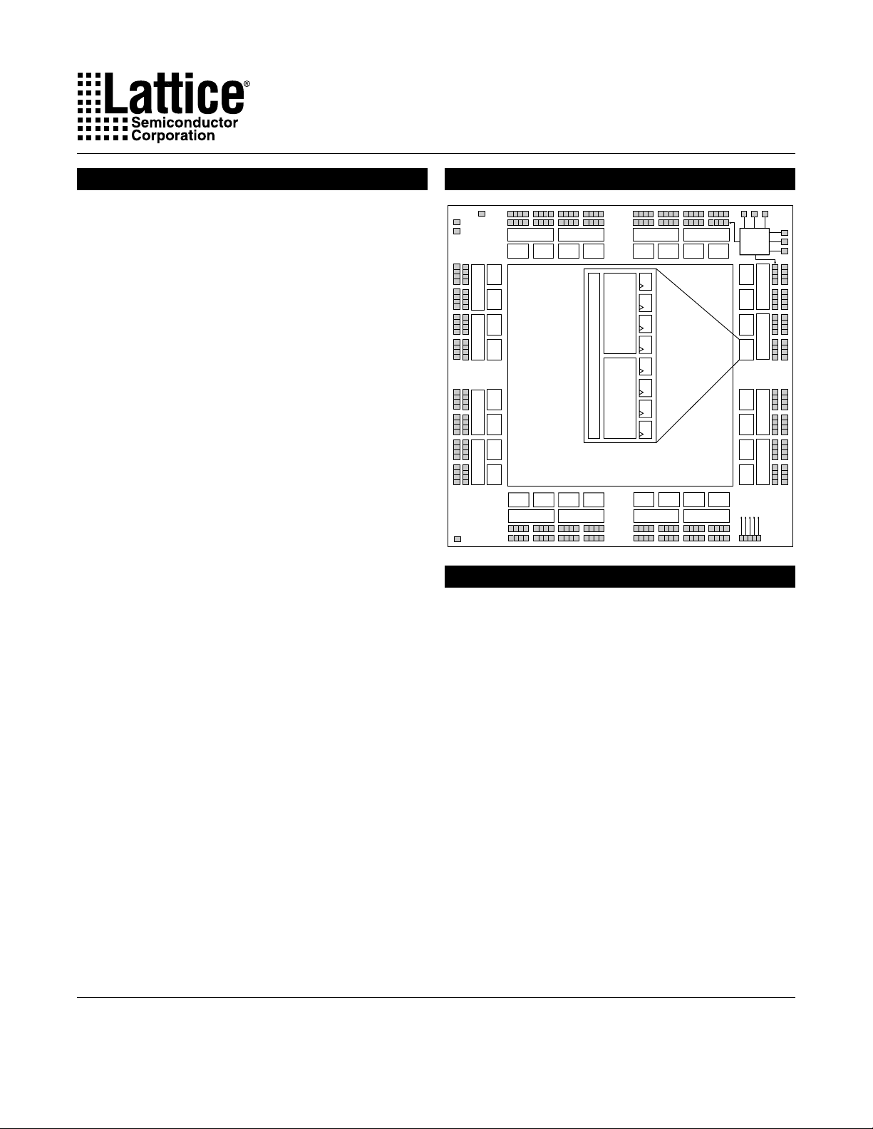
Functional Block Diagram
ORP
H3 H2 H1 H0
A0
A1
A2
ORP
A3
B0
ORP ORP
B1
B2
ORP
B3
C0 C1 C2 C3
ORP
ORP
OR
Array
AND Array
OR
Array
Global Routing Pool
ORP
ORP
G3
DQ
DQ
DQ
DQ
DQ
DQ
DQ
DQ
D0
ORP
ORP
G2 G1 G0
Twin
GLB
D1 D2
ORP
D3
Boundary
Scan
F3
F2
F1
F0
E3
ORP ORP
E2
E1
ORP ORP
E0
0139A/3256E
Description
The ispLSI 3256E is a High Density Programmable Logic
Device containing 512 Registers, 256 Universal I/O pins,
five Dedicated Clock Input Pins, 16 Output Routing Pools
(ORP) and a Global Routing Pool (GRP) which allows
complete inter-connectivity between all of these elements. The ispLSI 3256E features 5V in-system
programmability and in-system diagnostic capabilities.
The ispLSI 3256E offers non-volatile reprogrammability
of the logic, as well as the interconnect to provide truly
reconfigurable systems.
The basic unit of logic on the ispLSI 3256E device is the
Twin Generic Logic Block (Twin GLB) labelled A0, A1...H3.
There are a total of 32 Twin GLBs in the ispLSI 3256E
device. Each Twin GLB has 24 inputs, a programmable
AND array and two OR/Exclusive-OR Arrays and eight
outputs which can be configured to be either combinatorial or registered. All Twin GLB inputs come from the
GRP.
Copyright © 2002 Lattice Semiconductor Corp. All brand or product names are trademarks or registered trademarks of their respective holders. The specifications and information herein are subject
to change without notice.
LATTICE SEMICONDUCTOR CORP., 5555 Northeast Moore Ct., Hillsboro, Oregon 97124, U.S.A. June 2002
Tel. (503) 268-8000; 1-800-LATTICE; FAX (503) 268-8556; http://www.latticesemi.com
3256e_08 1
Page 2
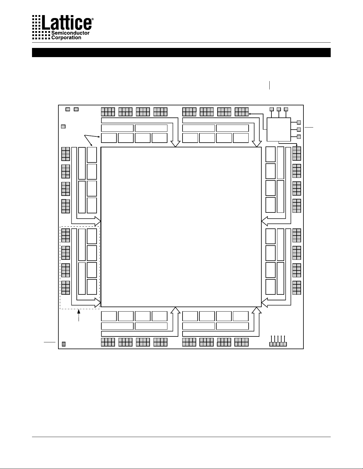
Functional Block Diagram
Figure 1. ispLSI 3256E Functional Block Diagram
I/O 255
I/O 253
I/O 251
I/O 249
I/O 247
I/O 245
I/O 243
GOE0
GOE1
I/O 254
I/O 252
I/O 250
I/O 248
I/O 246
I/O 244
I/O 241
I/O 242
I/O 240
I/O 239
I/O 237
I/O 238
I/O 236
I/O 235
I/O 233
I/O 234
I/O 232
I/O 231
I/O 229
I/O 230
I/O 228
I/O 227
I/O 226
I/O 225
I/O 224
Specifications ispLSI 3256E
I/O 223
I/O 221
I/O 219
I/O 217
I/O 215
I/O 213
I/O 211
I/O 222
I/O 220
I/O 218
I/O 216
I/O 214
I/O 212
I/O 209
I/O 210
I/O 208
I/O 207
I/O 205
I/O 206
I/O 204
I/O 203
I/O 201
I/O 202
I/O 200
I/O 199
I/O 197
I/O 198
I/O 196
I/O 195
I/O 193
I/O 194
I/O 192
BSCAN/ispEN
TCLK/SCLK
TMS/MODE
I/O 1
I/O 3
I/O 5
I/O 7
I/O 9
I/O 11
I/O 13
I/O 15
I/O 17
I/O 19
I/O 21
I/O 23
I/O 25
I/O 27
I/O 29
I/O 31
I/O 33
I/O 35
I/O 37
I/O 39
I/O 41
I/O 43
I/O 45
I/O 47
I/O 49
I/O 51
I/O 53
I/O 55
I/O 57
I/O 59
I/O 61
I/O 63
TOE
I/O 0
I/O 2
I/O 4
I/O 6
I/O 8
I/O 10
I/O 12
I/O 14
I/O 16
I/O 18
I/O 20
I/O 22
I/O 24
I/O 26
I/O 28
I/O 30
I/O 32
I/O 34
I/O 36
I/O 38
I/O 40
I/O 42
I/O 44
I/O 46
I/O 48
I/O 50
I/O 52
I/O 54
I/O 56
I/O 58
I/O 60
I/O 62
Generic
Logic
Blocks
A0
A1
A2
Input Bus
A3
B0
ORP ORP
B1
Input Bus
B2
ORP ORP
B3
ORP
H2 H1 H0
H3
Input Bus Input Bus
ORP ORP
ORP
G2 G1 G0
G3
Global Routing Pool
(GRP)
ISP and
Boundary
Scan TAP
F3
F2
F1
F0
E3
E2
E1
E0
ORP ORP
ORP ORP
TDI/SDI
TRST
TDO/SDO
Input Bus
Input Bus
I/O 190
I/O 188
I/O 186
I/O 184
I/O 182
I/O 180
I/O 178
I/O 176
I/O 174
I/O 172
I/O 170
I/O 168
I/O 166
I/O 164
I/O 162
I/O 160
I/O 158
I/O 156
I/O 154
I/O 152
I/O 150
I/O 148
I/O 146
I/O 144
I/O 142
I/O 140
I/O 138
I/O 136
I/O 134
I/O 132
I/O 130
I/O 128
I/O 191
I/O 189
I/O 187
I/O 185
I/O 183
I/O 181
I/O 179
I/O 177
I/O 175
I/O 173
I/O 171
I/O 169
I/O 167
I/O 165
I/O 163
I/O 161
I/O 159
I/O 157
I/O 155
I/O 153
I/O 151
I/O 149
I/O 147
I/O 145
I/O 143
I/O 141
I/O 139
I/O 137
I/O 135
I/O 133
I/O 131
I/O 129
RESET
Megablock
C1 C2 C3
C0
ORP ORP
ORP ORP
Input Bus Input Bus
I/O 88
I/O 90
I/O 92
I/O 64
I/O 66
I/O 65
I/O 67
I/O 68
I/O 70
I/O 69
I/O 71
I/O 72
I/O 74
I/O 73
I/O 75
I/O 76
I/O 78
I/O 77
I/O 79
I/O 80
I/O 82
I/O 81
I/O 83
I/O 84
I/O 85
I/O 86
I/O 87
I/O 89
I/O 91
I/O 94
I/O 93
I/O 95
2
D0
I/O 96
I/O 98
I/O 97
I/O 99
D1 D2 D3
I/O 100
I/O 102
I/O 104
I/O 106
I/O 108
I/O 110
I/O 101
I/O 103
I/O 105
I/O 107
I/O 109
I/O 111
I/O 112
I/O 114
I/O 113
I/O 115
I/O 116
I/O 118
I/O 117
I/O 119
I/O 120
I/O 122
I/O 121
I/O 123
I/O 124
I/O 126
I/O 125
I/O 127
CLK 1
CLK 0
Y0
Y1Y2Y3
IOCLK 1
CLK 2
IOCLK 0
Y4
0139isp/3256E
Page 3
Description (continued)
Specifications ispLSI 3256E
All local logic block outputs are brought back into the
GRP so they can be connected to the inputs of any other
logic block on the device. The device also has 256 I/O
cells, each of which is directly connected to an I/O pin.
Each I/O cell can be individually programmed to be a
combinatorial input, a registered input, a latched input, an
output or a bidirectional I/O pin with 3-state control. The
signal levels are TTL compatible voltages and the output
drivers can source 4 mA or sink 8 mA. Each output can
be programmed independently for fast or slow output
slew rate to minimize overall output switching noise.
The 256 I/O Cells are grouped into 16 sets of 16 bits.
Pairs of these I/O groups are associated with a logic
Megablock through the use of the ORP. Each Megablock
is able to provide one Product Term Output Enable
(PTOE) signal which is globally distributed to all I/O cells.
That PTOE signal can be generated within any GLB in the
Megablock. Each I/O cell can select either a Global OE
or a PTOE.
Four Twin GLBs, 32 I/O Cells and two ORPs are connected together to make a logic Megablock. The
Megablock is defined by the resources that it shares. The
outputs of the four Twin GLBs are connected to a set of
32 I/O cells by the ORP. The ispLSI 3256E device
contains eight of these Megablocks.
Clocks in the ispLSI 3256E device are provided through
five dedicated clock pins. The five pins provide three
clocks to the Twin GLBs and two clocks to the I/O cells.
The table below lists key attributes of the device along
with the number of resources available.
An additional feature of the ispLSI 3256E is its Boundary
Scan capability, which is composed of cells connected
between the on-chip system logic and the device’s input
and output pins. All I/O pins have associated boundary
scan registers, with 3-state I/O using three boundary
scan registers and inputs using one.
The ispLSI 3256E supports all IEEE 1149.1 mandatory
instructions, which include BYPASS, EXTEST and
SAMPLE.
Key Attributes of the ispLSI 3256E
etubirttAytitnauQ
sBLGniwT 23
sretsigeR 215
sniPO/I 652
skcolClabolG 5
The GRP has as its inputs the outputs from all of the Twin
GLBs and all of the inputs from the bidirectional I/O cells.
All of these signals are made available to the inputs of the
Twin GLBs. Delays through the GRP have been equalized to minimize timing skew and logic glitching.
EOlabolG 2
EOtseT 1
E6523/300-elbaT
3
Page 4
Specifications ispLSI 3256E
Absolute Maximum Ratings
1
Supply Voltage Vcc...........................................................................-0.5 to +7.0V
Input Voltage Applied........................................................................-2.5 to VCC +1.0V
Off-State Output Voltage Applied .....................................................-2.5 to VCC +1.0V
Storage Temperature........................................................................-65 to 150°C
Case Temp. with Power Applied ......................................................-55 to 125°C
Max. Junction Temp. (TJ) with Power Applied (304-Pin PQFP) ......150°C
Max. Junction Temp. (TJ) with Power Applied (320-Ball BGA)........140°C
1. Stresses above those listed under the “Absolute Maximum Ratings” may cause permanent damage to the device. Functional
operation of the device at these or at any other conditions above those indicated in the operational sections of this specification
is not implied (while programming, follow the programming specifications).
DC Recommended Operating Condition
T
V
V
V
A
SYMBOL
CC
IL
IH
PARAMETER
Ambient Temperature
Supply Voltage
Input Low Voltage
Input High Voltage
MIN. MAX. UNITS
0
4.75
0
2.0
70
5.25
0.8
V +1
CC
Table 2-0005/3256E
°C
V
V
V
Capacitance (TA=25°C,f=1.0 MHz)
SYMBOL
C
1
C
2
I/O Capacitance
Clock Capacitance
PARAMETER
Data Retention Specifications
PARAMETER
Data Retention
ispLSI Erase/Reprogram Cycles
UNITSTYPICAL TEST CONDITIONS
10
15
MINIMUM MAXIMUM UNITS
20
10000
pf V = 5.0V, V = 2.0V
pf V = 5.0V, V = 2.0V
–
–
CC I/O
CC Y
Table 2-0006/3256E
Years
Cycles
Table 2-0008/3256E
4
Page 5
Switching Test Conditions
Specifications ispLSI 3256E
Input Pulse Levels
Input Rise and Fall Time
Input Timing Reference Levels
Output Timing Reference Levels
Output Load
3-state levels are measured 0.5V from
GND to 3.0V
≤ 3ns 10% to 90%
1.5V
1.5V
See Figure 2
Table 2-0003/3256E
steady-state active level.
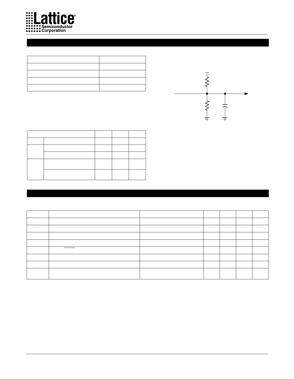
Output Load conditions (See Figure 2)
TEST CONDITION R1 R2 CL
A 470Ω 390Ω 35pF
Active High
B
Active Low
Active High to Z
at V -0.5V
C
Active Low to Z
at V +0.5V
OH
OL
∞ 390Ω 35pF
470Ω 390Ω 35pF
∞ 390Ω 5pF
470Ω 390Ω 5pF
DC Electrical Characteristics
Table 2 - 0004A
Figure 2. Test Load
Device
Output
*C
includes Test Fixture and Probe Capacitance.
L
+ 5V
R
1
Test
Point
R
2
C
*
L
0213A
Over Recommended Operating Conditions
SYMBOL
V
OL
V
OH
I
IL
I
IH
I
IL-isp
I
IL-PU
1
I
OS
2,4
I
CC
Output Low Voltage
Output High Voltage
Input or I/O Low Leakage Current
Input or I/O High Leakage Current
Bscan/ispEN Input Low Leakage Current
I/O Active Pull-Up Current
Output Short Circuit Current
Operating Power Supply Current
PARAMETER
I = 8 mA
OL
I = -4 mA
OH
0V ≤ V ≤ V (Max.)
3.5V ≤ V ≤ V
0V ≤ V ≤ V
0V ≤ V ≤ V
V = 5V, V = 0.5V
CC OUT
V = 0.0V, V = 3.0V
IL IH
f = 1 MHz
TOGGLE
1. One output at a time for a maximum duration of one second. V = 0.5V was selected to avoid test problems
CONDITION MIN. TYP. MAX. UNITS
–
IN IL
IN
IN IL
IN CC
IL
2.4
–
–
–
–
–
–
OUT
by tester ground degradation. Characterized but not 100% tested.
2. Measured using sixteen 16-bit counters.
3. Typical values are at V
4. Maximum I
varies widely with specific device configuration and operating frequency. Refer to the Power Consumption
CC
= 5V and TA = 25°C.
CC
section of this datasheet and Thermal Management section of the Lattice Semiconductor Data Book or CD-ROM to estimate
maximum I
CC
.
3
–
–
–
–
–
–
–
300
Table 2 - 0007isp/3256E
0.4
–
-10
10
-150
-150
-200
–
V
V
µA
µA
µA
µA
mA
mA
5
Page 6

Specifications ispLSI 3256E
External Switching Characteristics
Over Recommended Operating Conditions
5
TSET
RETEMARAP
t
1dp
t
2dp
f
xam
f
f
t
1us
t
1oc
t
1h
t
2us
t
2oc
t
2h
t
1r
t
1wr
t
neeotp
t
sideotp
t
neeog
t
sideog
t
neeot
t
sideot
t
hw
t
lw
t
3us
t
3h
—4 )1oct+2ust(/1,kcabdeeF.txEhtiw.qerFkcolC0.77—0.05— zHM
).txE(xam
—5 elggoTxaM,ycneuqerFkcolC
).goT(xam
—6 ssapybTP4,kcolCerofebemiTputeS.geRBLG5.5—0.9—sn
—8 ssapybTP4,kcolCretfaemiTdloH.geRBLG0.0—0.0—sn
—9 kcolCerofebemiTputeS.geRBLG5.6— 0.11—sn
—01yaleDtuptuOotkcolC.geRBLG—0.7— 0.01sn
—11kcolCretfaemiTdloH.geRBLG0.0—0.0—sn
—31noitaruDesluPteseR.txE5.6— 0.21—sn
—81elbanEtuptuOEOtseT—0.21—0.51sn
—91elbasiDtuptuOEOtseT—0.21—0.51sn
—02hgiH,noitaruDesluPkcolC.cnyS.txE0.5—0.6—sn
—12woL,noitaruDesluPkcolC.cnyS.txE0.5—0.6—sn
—22)4Y,3Y(kcolC.cnyS.txEerofebemiTputeS.geRO/I5.4—0.5—sn
—32)4Y,3Y(kcolC.cnyS.txEretfaemiTdloH.geRO/I0.0—0.0—sn
spe.E6523.txEgnimiT
2
#
.DNOC
A1 ssapyBPRO,ssapyBTP4,yaleD.porPataD—0.01—0.51sn
A2 yaleDnoitagaporPataD—0.31—0.81sn
A3 kcabdeeFlanretnIhtiwycneuqerFkcolC
A7 ssapybPRO,yaleDtuptuOotkcolC.geRBLG—5.6—0.9sn
A21yaleDtuptuOotniPteseR.txE—5.31—0.51sn
B41elbanEtuptuOottupnI—0.61—0.91sn
C51elbasiDtuptuOottupnI—0.61—0.91sn
B61elbanEtuptuOEOlabolG—0.9— 0.21sn
C71elbasiDtuptuOEOlabolG—0.9— 0.21sn
1, 2, 3
.kcabdeefPRGgnisuretnuoctib-61dradnatS.3
.noitcessnoitidnoCtseTgnihctiwSecnerefeR.5
1
NOITPIRCSED
3
4
.PROdnahtapROXTP02esusretemaraplla,esiwrehtodetonsselnU.1
.sliatedrehtrufrofteehsatadsihtniledoMgnimiTotrefeR.2
001-07-
.NIM.XAM.NIM.XAM
001—0.07— zHM
001—0.38— zHM
.%05nahtrehtofoelcycytudkcolcarofwollaotsisihT.)lwt+hwt(/1nahtsselebyam)elggoT(xamf.4
STINU
6
Page 7

Specifications ispLSI 3256E
Internal Timing Parameters
2
RETEMARAP
#
stupnI
t
pboi
t
taloi
t
usoi
t
hoi
t
ocoi
t
roi
PRG
t
prg
BLG
t
pbtp4
t
rbtp4
t
roxtp1
t
t
t
t
t
t
t
t
t
t
roxtp02
jdarox
pbg
usg
hg
ocg
org
ertp
eotp
kctp
PRO
pro
t
t
pbpro
42ssapyBretsigeRO/I—4.2—0.4sn
52yaleDhctaLO/I—3.01—0.41sn
62kcolCerofebemiTputeSretsigeRO/I8.4—8.5—sn
72kcolCretfaemiTdloHretsigeRO/I6.1-—5.2-—sn
82yaleDtuOotkcolCretsigeRO/I—8.5—5.8sn
92yaleDtuOotteseRretsigeRO/I—8.5—5.7sn
03yaleDPRG—3.2—2.3sn
13).bmoC(yaleDhtaPssapyBmreTtcudorP4—2.3—6.3sn
23).geR(yaleDhtaPssapyBmreTtcudorP4—1.3—8.4sn
33yaleDhtaPROX/mreTtcudorP1—0.4—1.5sn
43yaleDhtaPROX/mreTtcudorP02—1.4—2.5sn
53yaleDhtaPtnecajdAROX
63yaleDssapyBretsigeRBLG—5.1—6.1sn
73kcolCerofebemiTputeSretsigeRBLG3.0—2.1—sn
83kcolCretfaemiTdloHretsigeRBLG0.5—6.7—sn
93yaleDtuptuOotkcolCretsigeRBLG—6.1—0.3sn
04yaleDtuptuOotteseRretsigeRBLG—2.5—2.5sn
14yaleDretsigeRotteseRmreTtcudorPBLG—0.4—4.4sn
24yaleDlleCO/IotelbanEtuptuOmreTtcudorPBLG—5.6—9.6sn
34yaleDkcolCmreTtcudorPBLG0.36.34.32.4sn
44yaleDPRO—2.1—9.1sn
54yaleDssapyBPRO—7.0—9.0sn
spe.E6523.tnIgnimiT
1
Over Recommended Operating Conditions
NOITPIRCSED
3
.ylnoecnereferroferadnadetsettonerasretemaraPgnimiTlanretnI.1
.sliatedrehtrufrofteehsatadsihtniledoMgnimiTotrefeR.2
.sorcamdrahybdesuebylnonachtaptnecajdaROXehT.3
001-07-
.NIM.XAM.NIM.XAM
—3.4—7.5sn
STINU
7
Page 8

Specifications ispLSI 3256E
Internal Timing Parameters
Over Recommended Operating Conditions
2
RETEMARAP
#
stuptuO
t
bo
t
sbo
t
neo
t
sido
skcolC
t
2/1/0yg
t
4/3yoi
t
rg
t
eog
t
eot
64yaleDreffuBtuptuO—6.2—3.3sn
74reddAdetimiLwelS,yaleDreffuBtuptuO—6.71—3.81sn
84delbanEtuptuOotEOlleCO/I—5.5—7.5sn
94delbasiDtuptuOotEOlleCO/I—5.5—7.5sn
05eniLklCBLGlabolGot2Yro1Yro0Y,yaleDkcolC6.16.18.18.1sn
15eniLkcolClabolGlleCO/Iot4Yro3Y,yaleDkcolC3.06.18.05.2sn
teseRlabolG
25sretsigeRO/IdnaBLGotteseRlabolG—5.4—6.4sn
35reffuBdaPEOlabolG—9.5—5.7sn
45reffuBdaPEOtseT—1.6—9.8sn
spe.E6523.2.tnIgnimiT
1
NOITPIRCSED
.ylnoecnereferroferadnadetsettonerasretemaraPgnimiTlanretnI.1
.sliatedrehtrufrofteehsatadsihtniledoMgnimiTotrefeR.2
001-07-
.NIM.XAM.NIM.XAM
STINU
8
Page 9

ispLSI 3256E Timing Model
#52
I/O Reg Bypass
#24
Input
Register
D
RST
#25 - 29
#51
Q
I/O Pin
(Input)
Reset
Y3,4
GRP
#30
Feedback
4 PT Bypass
#32
20 PT
XOR Delays
#33 - 35
#52
Control
PTs
#41 - 43
Specifications ispLSI 3256E
#31
RE
OE
CK
GLB Reg Bypass ORP Bypass
#36
GLB Reg
Delay
DQ
RST
#37 - 40
#45
ORP
Delay
#44
#46, 47
I/O CellORPGLBGRPI/O Cell
I/O Pin
(Output)
#48, 49
Y0,1,2
GOE0,1
TOE
Derivations of tsu, th and tco from the Product Term Clock
t
su Logic + Reg su - Clock (min)
t
hClock (max) + Reg h - Logic
t
co Clock (max) + Reg co + Output
=
t
iobp + tgrp + t20ptxor) + (tgsu) - (tiobp + tgrp + tptck(min))
=
(
(#24+ #30+ #34) + (#37) - (#24+ #30+ #43)
=
(2.4 + 2.3 + 4.1) + (0.3) - (2.4 + 2.3 + 3.0)1.4 ns
=
=
t
iobp + tgrp + tptck(max)) + (tgh) - (tiobp + tgrp + t20ptxor)
(
=
(#24+ #30+ #43) + (#38) - (#24+ #30+ #34)
=
(2.4 + 2.3 + 3.6) + (5.0) - (2.4 + 2.3 + 4.1)4.5 ns
=
=
t
iobp + tgrp + tptck(max)) + (tgco) + (torp + tob)
(
=
(#24 + #30 + #43) + (#39) + (#44 + #46)
=
(2.4 + 2.3 + 3.6) + (1.6) + (1.2 + 2.6)13.7 ns
=
#50
#53
#54
1
Table 2- 0042-3256E
Note: Calculations are based upon timing specifications for the ispLSI 3256E-100L.
0902/3256E
9
Page 10

Power Consumption
Specifications ispLSI 3256E
Power consumption in the ispLSI 3256E device depends
on two primary factors: the speed at which the device is
operating and the number of product terms used.
Figure 3. Typical Device Power Consumption vs fmax
600
500
400
(mA)
CC
I
300
200
020406080100
f
max (MHz)
Notes: Configuration of 16 16-bit Counters
Typical Current at 5V, 25° C
Figure 3 shows the relationship between power and
operating speed.
ispLSI 3256E
ICC can be estimated for the ispLSI 3256E using the following equation:
ICC = 60 + (# of PTs * 0.48) + (# of nets * Max. freq * 0.0106) where:
# of PTs = Number of Product Terms used in design
# of nets = Number of Signals used in device
Max. freq = Highest Clock Frequency to the device
The I
GLB loads on average exists. These values are for estimates only. Since the value of I
operating conditions and the program in the device, the actual I
estimate is based on typical conditions (VCC = 5.0V, room temperature) and an assumption of two
CC
should be verified.
CC
is sensitive to
CC
10
Page 11

Specifications ispLSI 3256E
Pin Description
Pin Name Description
I/O Input/Output pins – These are the general purpose I/O pins used by the logic array.
GOE0, GOE1 Global Output Enable input pins.
TOE Test Output Enable pin – This pin tristates all I/O pins when a logic low is driven.
RESET Active Low (0) Reset pin – Resets all of the GLB and I/O registers in the device.
Y0, Y1, Y2 Dedicated Clock inputs. These clock inputs are connected to one of the clock inputs of all the GLBs on
the device.
Y3, Y4 Dedicated Clock inputs. These clock inputs are connected to one of the clock inputs of all the I/O cells
on the device.
BSCAN/ispEN Input – Dedicated in-system programming enable input pin. When this pin is high, the BSCAN TAP
controller pins TMS, TDI, TDO and TCK are enabled. When this pin is brought low, the ISP State
Machine control pins MODE, SDI, SDO and SCLK are enabled. High-to-low transition of this pin will put
the device in the programming mode and put all I/O pins in the high-Z state.
TDI/SDI Input – This pin performs two functions. It is the Test Data input pin when ispEN is logic high. When
ispEN is logic low, it functions as an input pin to load programming data into the device. SDI is also
used as one of the two control pins for the ISP State Machine.
TCK/SCLK Input – This pin performs two functions. It is the Test Clock input pin when ispEN is logic high. When
ispEN is logic low, it functions as a clock pin for the Serial Shift Register.
TMS/MODE Input – This pin performs two functions. It is the Test Mode Select input pin when ispEN is logic high.
When ispEN is logic low, it functions as a pin to control the operation of the ISP State Machine.
TRST/NC
1
TDO/SDO Output – This pin performs two functions. When ispEN is logic low, it functions as the pin to read the
GND Ground (GND)
VCC Vcc
1
NC
1. NC pins are not to be connected to any active signals, VCC or GND.
Input – Test Reset, active low to reset the Boundary Scan State Machine.
ISP data. When ispEN is high, it functions as Test Data Out.
No Connect.
Pin Locations
Signal 304-Pin PQFP 320-Ball BGA
GOE0, GOE1 195, 185 AD11, AC14
TOE 215 AC6
RESET 53 A17
Y0, Y1, Y2, Y3, Y4 43, 33, 205, 175, 165 A14, B11, AD8, AB16, AA18
ispEN/BSCAN 63 B19
SDI/TDI 23 C9
SCLK/TCK 73 D20
MODE/TMS 13 D7
TRST/NC
1
SDO/TDO 155 AB21
GND 9, 19, 39, 49, 69, 85, 95, 115, 125, 145, 161, 171, D6, C8, B13, A16, D19, F21, H22, N23, T24, W21,
VCC 1, 29, 59, 77, 105, 135, 153, 181, 211, 229, 257, D4, B10, B18, D21, K23, V23, AA21, AC15, AC7,
1
NC
1. NC pins are not to be connected to any active signals, VCC or GND.
225 AA5
191, 201, 221, 237, 247, 267, 277, 297 AA19, AB17, AC12, AD9, AA6, W4, U3, M2, J1, F4
287, 304 AA4, R2, G2, C3
A1, A2, A23, A24, B1, B2, B23, B24, AC1, AC2,
AC23, AC24, AD1, AD2, AD23, AD24
11
Page 12

I/O Locations
Specifications ispLSI 3256E
Signal PQFP BGA
I/O 0 40 C13
I/O 1 41 D13
I/O 2 42 A13
I/O 3 44 B14
I/O 4 45 C14
I/O 5 46 D14
I/O 6 47 A15
I/O 7 48 B15
I/O 8 50 C15
I/O 9 51 D15
I/O 10 52 B16
I/O 11 54 C16
I/O 12 55 B17
I/O 13 56 D16
I/O 14 57 A18
I/O 15 58 C17
I/O 16 60 A19
I/O 17 61 D17
I/O 18 62 C18
I/O 19 64 A20
I/O 20 65 D18
I/O 21 66 C19
I/O 22 67 B20
I/O 23 68 A21
I/O 24 70 C20
I/O 25 71 B21
I/O 26 72 A22
I/O 27 74 C21
I/O 28 75 B22
I/O 29 76 C22
I/O 30 78 C23
I/O 31 79 D22
I/O 32 80 C24
I/O 33 81 E21
I/O 34 82 D23
I/O 35 83 E22
I/O 36 84 D24
I/O 37 86 E23
I/O 38 87 F22
I/O 39 88 E24
I/O 40 89 G21
I/O 41 90 F23
I/O 42 91 G22
I/O 43 92 F24
I/O 44 93 H21
I/O 45 94 G23
I/O 46 96 G24
I/O 47 97 J21
I/O 48 98 H23
I/O 49 99 J22
I/O 50 100 H24
I/O 51 101 J23
I/O 52 102 K21
Signal PQFP BGA
I/O 53 103 K22
I/O 54 104 J24
I/O 55 106 K24
I/O 56 107 L21
I/O 57 108 L22
I/O 58 109 L23
I/O 59 110 L24
I/O 60 111 M24
I/O 61 112 M21
I/O 62 113 M22
I/O 63 114 M23
I/O 64 116 N22
I/O 65 117 N21
I/O 66 118 N24
I/O 67 119 P24
I/O 68 120 P23
I/O 69 121 P22
I/O 70 122 P21
I/O 71 123 R24
I/O 72 124 R23
I/O 73 126 R22
I/O 74 127 R21
I/O 75 128 T23
I/O 76 129 U24
I/O 77 130 T22
I/O 78 131 U23
I/O 79 132 T21
I/O 80 133 V24
I/O 81 134 U22
I/O 82 136 W24
I/O 83 137 U21
I/O 84 138 V22
I/O 85 139 W23
I/O 86 140 Y24
I/O 87 141 V21
I/O 88 142 W22
I/O 89 143 Y23
I/O 90 144 AA24
I/O 91 146 Y22
I/O 92 147 AA23
I/O 93 148 AB24
I/O 94 149 Y21
I/O 95 150 AA22
I/O 96 151 AB23
I/O 97 152 AB22
I/O 98 154 AC22
I/O 99 156 AD22
I/O 100 157 AA20
I/O 101 158 AC21
I/O 102 159 AB20
I/O 103 160 AD21
I/O 104 162 AC20
I/O 105 163 AB19
Signal PQFP BGA Signal PQFP BGA Signal PQFP BGA
I/O 106 164 AD20
I/O 107 166 AC19
I/O 108 167 AB18
I/O 109 168 AD19
I/O 110 169 AA17
I/O 111 170 AC18
I/O 112 172 AD18
I/O 113 173 AA16
I/O 114 174 AC17
I/O 115 176 AD17
I/O 116 177 AC16
I/O 117 178 AA15
I/O 118 179 AB15
I/O 119 180 AD16
I/O 120 182 AD15
I/O 121 183 AA14
I/O 122 184 AB14
I/O 123 186 AD14
I/O 124 187 AD13
I/O 125 188 AA13
I/O 126 189 AB13
I/O 127 190 AC13
I/O 128 192 AB12
I/O 129 193 AA12
I/O 130 194 AD12
I/O 131 196 AC11
I/O 132 197 AB11
I/O 133 198 AA11
I/O 134 199 AD10
I/O 135 200 AC10
I/O 136 202 AB10
I/O 137 203 AA10
I/O 138 204 AC9
I/O 139 206 AB9
I/O 140 207 AC8
I/O 141 208 AA9
I/O 142 209 AD7
I/O 143 210 AB8
I/O 144 212 AD6
I/O 145 213 AA8
I/O 146 214 AB7
I/O 147 216 AD5
I/O 148 217 AA7
I/O 149 218 AB6
I/O 150 219 AC5
I/O 151 220 AD4
I/O 152 222 AB5
I/O 153 223 AC4
I/O 154 224 AD3
I/O 155 226 AB4
I/O 156 227 AC3
I/O 157 228 AB3
I/O 158 230 AB2
I/O 159 231 AA3
I/O 160 232 AB1
I/O 161 233 Y4
I/O 162 234 AA2
I/O 163 235 Y3
I/O 164 236 AA1
I/O 165 238 Y2
I/O 166 239 W3
I/O 167 240 Y1
I/O 168 241 V4
I/O 169 242 W2
I/O 170 243 V3
I/O 171 244 W1
I/O 172 245 U4
I/O 173 246 V2
I/O 174 248 V1
I/O 175 249 T4
I/O 176 250 U2
I/O 177 251 T3
I/O 178 252 U1
I/O 179 253 T2
I/O 180 254 R4
I/O 181 255 R3
I/O 182 256 T1
I/O 183 258 R1
I/O 184 259 P4
I/O 185 260 P3
I/O 186 261 P2
I/O 187 262 P1
I/O 188 263 N1
I/O 189 264 N4
I/O 190 265 N3
I/O 191 266 N2
I/O 192 268 M3
I/O 193 269 M4
I/O 194 270 M1
I/O 195 271 L1
I/O 196 272 L2
I/O 197 273 L3
I/O 198 274 L4
I/O 199 275 K1
I/O 200 276 K2
I/O 201 278 K3
I/O 202 279 K4
I/O 203 280 J2
I/O 204 281 H1
I/O 205 282 J3
I/O 206 283 H2
I/O 207 284 J4
I/O 208 285 G1
I/O 209 286 H3
I/O 210 288 F1
I/O 211 289 H4
I/O 212 290 G3
I/O 213 291 F2
I/O 214 292 E1
I/O 215 293 G4
I/O 216 294 F3
I/O 217 295 E2
I/O 218 296 D1
I/O 219 298 E3
I/O 220 299 D2
I/O 221 300 C1
I/O 222 301 E4
I/O 223 302 D3
I/O 224 303 C2
I/O 225 2 B3
I/O 226 3 C4
I/O 227 4 A3
I/O 228 5 D5
I/O 229 6 B4
I/O 230 7 C5
I/O 231 8 A4
I/O 232 10 B5
I/O 233 11 C6
I/O 234 12 A5
I/O 235 14 B6
I/O 236 15 C7
I/O 237 16 A6
I/O 238 17 D8
I/O 239 18 B7
I/O 240 20 A7
I/O 241 21 D9
I/O 242 22 B8
I/O 243 24 A8
I/O 244 25 B9
I/O 245 26 D10
I/O 246 27 C10
I/O 247 28 A9
I/O 248 30 A10
I/O 249 31 D11
I/O 250 32 C11
I/O 251 34 A11
I/O 252 35 A12
I/O 253 36 D12
I/O 254 37 C12
I/O 255 38 B12
12
Page 13

Pin Configuration
ispLSI 3256E 304-Pin PQFP Pinout Diagram
VCC
I/O 224
I/O 223
I/O 222
I/O 221
I/O 220
I/O 219
GND
I/O 218
I/O 217
I/O 216
I/O 215
I/O 214
I/O 213
I/O 212
I/O 211
I/O 210
VCC
I/O 209
I/O 208
I/O 207
I/O 206
I/O 205
I/O 204
I/O 203
I/O 202
I/O 201
304
303
302
301
300
299
298
297
296
295
294
293
292
291
290
289
288
287
286
285
284
283
282
281
280
279
VCC
I/O 225
I/O 226
I/O 227
I/O 228
I/O 229
I/O 230
I/O 231
GND
I/O 232
I/O 233
I/O 234
MODE/TMS
I/O 235
I/O 236
I/O 237
I/O 238
I/O 239
GND
I/O 240
I/O 241
I/O 242
SDI/TDI
I/O 243
I/O 244
I/O 245
I/O 246
I/O 247
VCC
I/O 248
I/O 249
I/O 250
I/O 251
I/O 252
I/O 253
I/O 254
I/O 255
GND
I/O 0
I/O 1
I/O 2
I/O 3
I/O 4
I/O 5
I/O 6
I/O 7
GND
I/O 8
I/O 9
I/O 10
RESET
I/O 11
I/O 12
I/O 13
I/O 14
I/O 15
VCC
I/O 16
I/O 17
I/O 18
ispEN/BSCAN
I/O 19
I/O 20
I/O 21
I/O 22
I/O 23
GND
I/O 24
I/O 25
I/O 26
SCLK/TCK
I/O 27
I/O 28
I/O 29
1
2
3
4
5
6
7
8
9
10
11
12
13
14
15
16
17
18
19
20
21
22
23
24
25
26
27
28
29
30
31
32
33
Y1
34
35
36
37
38
39
40
41
42
43
Y0
44
45
46
47
48
49
50
51
52
53
54
55
56
57
58
59
60
61
62
63
64
65
66
67
68
69
70
71
72
73
74
75
76
7778798081828384858687888990919293949596979899
278
100
101
102
103
Specifications ispLSI 3256E
GND
I/O 200
I/O 199
I/O 198
I/O 197
I/O 196
I/O 195
I/O 194
I/O 193
I/O 192
GND
I/O 191
I/O 190
I/O 189
I/O 188
I/O 187
I/O 186
277
276
275
274
273
272
271
270
269
268
267
266
265
264
263
262
261
ispLSI 3256E
Top View
104
105
106
107
108
109
110
111
112
113
114
115
116
117
118
119
120
I/O 185
I/O 184
260
259
121
122
I/O 183
VCC
258
257
123
124
I/O 182
I/O 181
256
255
125
126
I/O 180
254
127
I/O 179
I/O 178
253
252
128
129
I/O 177
I/O 176
251
250
130
131
I/O 175
I/O 174
249
248
132
133
GND
247
134
I/O 173
I/O 172
246
245
135
136
I/O 171
I/O 170
244
243
137
138
I/O 169
I/O 168
242
241
139
140
I/O 167
I/O 166
240
239
141
142
I/O 165
GND
238
237
143
144
I/O 164
I/O 163
236
235
145
146
I/O 162
I/O 161
234
233
147
148
I/O 160
232
149
I/O 159
I/O 158
231
230
150
151
VCC
229
152
228
I/O 157
227
I/O 156
226
I/O 155
TRST/NC
I/O 154
I/O 153
I/O 152
GND
I/O 151
I/O 150
I/O 149
I/O 148
I/O 147
TOE
I/O 146
I/O 145
I/O 144
VCC
I/O 143
I/O 142
I/O 141
I/O 140
I/O 139
Y2
I/O 138
I/O 137
I/O 136
GND
I/O 135
I/O 134
I/O 133
I/O 132
I/O 131
GOE0
I/O 130
I/O 129
I/O 128
GND
I/O 127
I/O 126
I/O 125
I/O 124
I/O 123
GOE1
I/O 122
I/O 121
I/O 120
VCC
I/O 119
I/O 118
I/O 117
I/O 116
I/O 115
Y3
I/O 114
I/O 113
I/O 112
GND
I/O 111
I/O 110
I/O 109
I/O 108
I/O 107
Y4
I/O 106
I/O 105
I/O 104
GND
I/O 103
I/O 102
I/O 101
I/O 100
I/O 99
SDO/TDO
I/O 98
VCC
1
225
224
223
222
221
220
219
218
217
216
215
214
213
212
211
210
209
208
207
206
205
204
203
202
201
200
199
198
197
196
195
194
193
192
191
190
189
188
187
186
185
184
183
182
181
180
179
178
177
176
175
174
173
172
171
170
169
168
167
166
165
164
163
162
161
160
159
158
157
156
155
154
153
VCC
I/O 30
I/O 31
I/O 32
I/O 33
I/O 34
I/O 35
I/O 36
GND
I/O 37
I/O 38
I/O 39
I/O 40
I/O 41
I/O 42
I/O 43
I/O 44
I/O 45
GND
I/O 46
I/O 47
I/O 48
I/O 49
I/O 50
I/O 51
I/O 52
I/O 53
I/O 54
VCC
I/O 55
I/O 56
I/O 57
I/O 58
I/O 59
1. NC pins are not to be connected to any active signals, VCC or GND.
I/O 60
I/O 61
13
I/O 62
I/O 63
GND
I/O 64
I/O 65
I/O 66
I/O 67
I/O 68
I/O 69
I/O 70
I/O 71
I/O 72
GND
I/O 73
I/O 74
I/O 75
I/O 76
I/O 77
I/O 78
I/O 79
I/O 80
I/O 81
VCC
I/O 82
I/O 83
I/O 84
I/O 85
I/O 86
I/O 87
I/O 88
I/O 89
I/O 90
GND
I/O 91
I/O 92
I/O 93
I/O 94
I/O 95
I/O 96
I/O 97
304MQFP.3256E
Page 14

Signal Configuration
ispLSI 3256E 320-Ball BGA Signal Diagram
24 23 22 21 20 19 18 17 16 15 14 13 12 11 10 987654321
Specifications ispLSI 3256E
A
B
C
D
E
F
G
H
J
K
L
M
N
P
R
T
U
V
W
Y
AA
AB
AC
AD
NC1NC
I/O
I/O
I/O
1
1
NC
NC
I/O32I/O30I/O29I/O27I/O24I/O21I/O18I/O15I/O11I/O8I/O4I/O0I/O
I/O
I/O
34
36
I/O37I/O35I/O
I/O
39
I/O41I/O
I/O
43
I/O45I/O42I/O
I/O
46
I/O50I/O
48
I/O54I/O51I/O49I/O
I/O
VCC
55
I/O59I/O58I/O57I/O
I/O
I/O
63
60
I/O
GND
66
I/O
I/O
68
67
I/O71I/O
72
I/O75I/O77I/O
GND
I/O
I/O
78
76
I/O
VCC
80
I/O
I/O
85
82
I/O86I/O89I/O91I/O
I/O
I/O
92
90
I/O93I/O96I/O
1
1
NC
NC
1
1
NC
NC
28
I/O
31
38
GND
I/O
53
I/O
62
I/O64I/O
I/O
69
I/O73I/O
I/O
81
I/O84I/O
I/O
88
I/O
95
97
I/O
98
I/O99I/O
25
VCC
33
GND
40
I/O
44
47
I/O
52
56
I/O
61
65
I/O
70
74
79
I/O
83
87
GND
94
VCC
SDO/
TDO
I/O
101
103
22
SCLK/
TCK
I/O
100
I/O
102
I/O
104
I/O
106
ispEN/
BSCAN
GND
I/O
105
I/O
107
I/O
109
14
I/O
20
Y4GND
I/O
108
I/O
111
I/O
112
RESET
I/O
12
I/O
17
I/O
110
GND Y3
I/O
114
I/O
115
I/O26I/O23I/O19I/O16I/O
1
I/O
GND Y0
6
I/O
I/O
7
10
I/O
I/O
9
13
I/O
I/O
3
5
I/O2I/O
I/O
1
ispLSI 3256E
Bottom View
I/O
I/O
I/O
I/O
113
I/O
116
I/O
119
117
I/O
118
I/O
120
121
I/O
122
GOE
1
I/O
123
125
I/O
126
I/O
127
I/O
124
252
I/O
255
254
I/O
253
I/O
129
I/O
128
I/O
130
I/O
I/O
I/O
I/O
I/O
I/O
I/O
251
248
247
243
240
237
I/O
I/O
I/O
I/O
VCCGNDVCC Y1 NC
I/O
I/O
250
246
I/O
I/O
245
249
I/O
I/O
137
133
I/O
I/O
132
136
I/O
I/O
135
131
I/O
GOE
134
0
242
244
SDI/
GND VCC
TDI
I/O
I/O
238
241
I/O
I/O
145
141
I/O
I/O
139
143
I/O
I/O
140
138
GND Y2
239
I/O
236
MODE/
TMS
I/O
148
I/O
146
I/O
142
235
233
149
TOEVCCGNDVCC
144
I/O
I/O
I/O
234
I/O
232
I/O
230
I/O
228
TRST/
NC
I/O
152
I/O
150
I/O
147
I/O
231
I/O
229
I/O
226
VCCGND
I/O
222
GND
I/O
215
I/O
211
I/O
207
I/O
202
I/O
198
I/O
193
I/O
189
I/O
184
I/O
180
I/O
175
I/O
GND
172
I/O
168
GND
I/O
161
VCCGND
1
I/O
155
I/O
153
I/O
151
I/O
227
I/O
225
I/O
223
I/O
219
I/O
216
I/O
212
I/O
209
I/O
205
I/O
201
I/O
197
I/O
192
I/O
190
I/O
185
I/O
181
I/O
177
I/O
170
I/O
166
I/O
163
I/O
159
I/O
157
I/O
156
I/O
154
NC1NC
1
NC
I/O
224
I/O
220
I/O
217
I/O
213
VCC
I/O
206
I/O
GND
203
I/O
200
I/O
196
GND
I/O
191
I/O
186
VCC
I/O
179
I/O
176
I/O
173
I/O
169
I/O
165
I/O
162
I/O
158
1
NC
1
NC
I/O
221
I/O
218
I/O
214
I/O
210
I/O
208
I/O
204
I/O
199
I/O
195
I/O
194
I/O
188
I/O
187
I/O
183
I/O
182
I/O
178
I/O
174
I/O
171
I/O
167
I/O
164
I/O
160
NC
NC
1
A
1
B
C
D
E
F
G
H
J
K
L
M
N
P
R
T
U
V
W
Y
AA
AB
1
AC
1
AD
24 23 22 21 20 19 18 17 16 15 14 13 12 11 10 987654321
1. NC pins are not to be connected to any active signals, VCC or GND.
Note: Ball A1 indicator dot on top side of package.
14
Page 15

Part Number Description
Specifications ispLSI 3256E
Device Family
Device Number
Speed
f
max
f
100 = 100 MHz
70 = 70 MHz
Ordering Information
FAMILY fmax (MHz)
100
ispLSI
100 320-Ball BGA10 ispLSI 3256E-100LB320
70
70 320-Ball BGA15 ispLSI 3256E-70LB320
ispLSI 3256E XXX X XXXX
–
max
COMMERCIAL
tpd (ns)
10
15
ORDERING NUMBER PACKAGE
ispLSI 3256E-100LQ
ispLSI 3256E-70LQ
X
Grade
Blank = Commercial
Package
P = PQFP
B320 = BGA
Power
L = Low
0212/3256E
304-Pin PQFP
304-Pin PQFP
Table 2-0041/3256E
15
 Loading...