

Datasheet ISPLSI3256A-90LQ, ISPLSI3256A-90LM, ISPLSI3256A-70LQI, ISPLSI3256A-70LQ, ISPLSI3256A-70LM Datasheet (Lattice Semiconductor Corporation)
...Page 1
®
ispLSI
3256A
In-System Programmable High Density PLD
Features
• HIGH-DENSITY PROGRAMMABLE LOGIC
— 128 I/O Pins
— 11000 PLD Gates
— 384 Registers
— High Speed Global Interconnect
— Wide Input Gating for Fast Counters, State
Machines, Address Decoders, etc.
— Small Logic Block Size for Random Logic
2
• HIGH-PERFORMANCE E
—
fmax = 90 MHz Maximum Operating Frequency
tpd = 12 ns Propagation Delay
—
— TTL Compatible Inputs and Outputs
— Electrically Erasable and Reprogrammable
— Non-Volatile
— 100% Tested at Time of Manufacture
— Unused Product Term Shutdown Saves Power
• IN-SYSTEM PROGRAMMABLE
— 5V In-System Programmable (ISP™) using Lattice
ISP or Boundary Scan Test (IEEE 1149.1) Protocol
— Increased Manufacturing Yields, Reduced Time-to-
Market, and Improved Product Quality
— Reprogram Soldered Devices for Faster Debugging
• 100% IEEE 1149.1 BOUNDARY SCAN COMPATIBLE
• OFFERS THE EASE OF USE AND FAST SYSTEM
SPEED OF PLDs WITH THE DENSITY AND FLEXIBILITY
OF FIELD PROGRAMMABLE GATE ARRAYS
— Complete Programmable Device Can Combine Glue
Logic and Structured Designs
— Enhanced Pin Locking Capability
— Five Dedicated Clock Input Pins
— Synchronous and Asynchronous Clocks
— Programmable Output Slew Rate Control to Mini-
mize Switching Noise
— Flexible Pin Placement
— Optimized Global Routing Pool Provides Global
Interconnectivity
• ispDesignEXPERT™ – LOGIC COMPILER AND COMPLETE ISP DEVICE DESIGN SYSTEMS FROM HDL
SYNTHESIS THROUGH IN-SYSTEM PROGRAMMING
— Superior Quality of Results
— Tightly Integrated with Leading CAE Vendor Tools
— Productivity Enhancing Timing Analyzer, Explore
Tools, Timing Simulator and ispANALYZER™
— PC and UNIX Platforms
CMOS® TECHNOLOGY
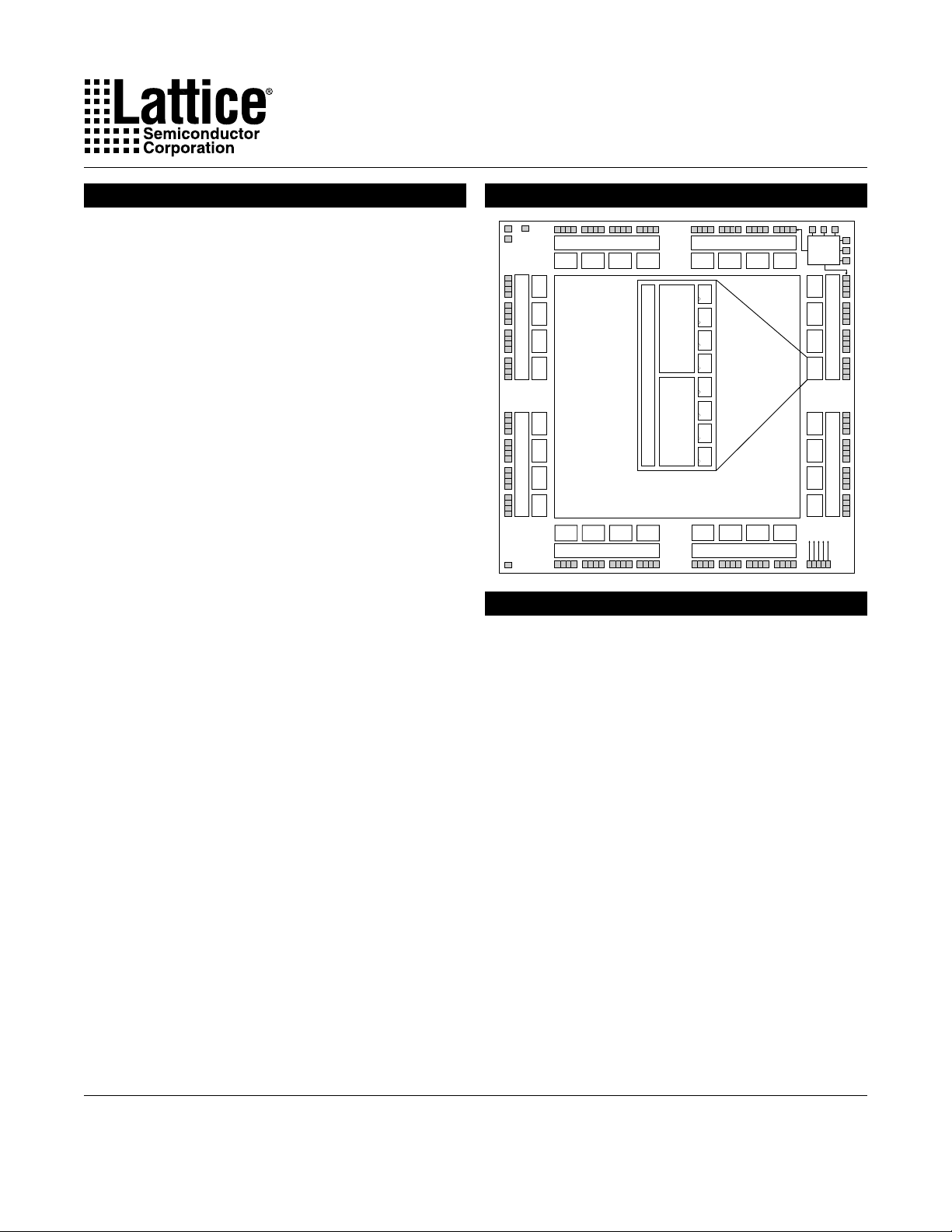
Functional Block Diagram
Output Routing Pool
H3 H2 H1 H0
A0
A1
A2
A3
Output Routing Pool
B0
B1
B2
B3
Output Routing Pool
C0 C1 C2 C3
Output Routing Pool
AND Array
Global Routing Pool
Output Routing Pool
G3
DQ
DQ
OR
Array
DQ
DQ
DQ
DQ
OR
Array
DQ
DQ
D0
Output Routing Pool
G2 G1 G0
Twin
GLB
D1 D2
D3
Boundary
Scan
F3
F2
F1
F0
Output Routing Pool
E3
E2
E1
E0
Output Routing Pool
0139A
Description
The ispLSI 3256A is a High-Density Programmable Logic
Device containing 384 Registers, 128 Universal I/O pins,
five Dedicated Clock Input Pins, eight Output Routing
Pools (ORP) and a Global Routing Pool (GRP) which
allows complete inter-connectivity between all of these
elements. The ispLSI 3256A features 5V in-system
programmability and in-system diagnostic capabilities.
The ispLSI 3256A offers non-volatile reprogrammability
of the logic, as well as the interconnect to provide truly
reconfigurable systems.
The basic unit of logic on the ispLSI 3256A device is the
Twin Generic Logic Block (Twin GLB) labelled A0, A1...H3.
There are a total of 32 Twin GLBs in the ispLSI 3256A
device. Each Twin GLB has 24 inputs, a programmable
AND array and two OR/Exclusive-OR Arrays, and eight
outputs which can be configured to be either combinatorial or registered. All Twin GLB inputs come from the
GRP.
Copyright © 1999 Lattice Semiconductor Corp. All brand or product names are trademarks or registered trademarks of their respective holders. The specifications and information herein are subject
to change without notice.
LATTICE SEMICONDUCTOR CORP., 5555 Northeast Moore Ct., Hillsboro, Oregon 97124, U.S.A. May 1999
Tel. (503) 268-8000; 1-800-LATTICE; FAX (503) 268-8556; http://www.latticesemi.com
3256a_09 1
Page 2
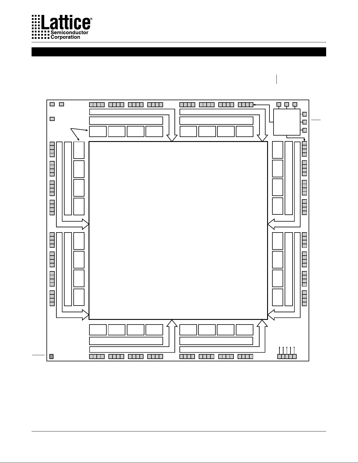
Functional Block Diagram
Figure 1. ispLSI 3256A Functional Block Diagram
GOE0
GOE1
I/O 127
I/O 126
I/O 125
I/O 124
I/O 123
I/O 122
I/O 121
I/O 120
I/O 119
I/O 118
I/O 117
I/O 116
I/O 115
I/O 114
I/O 113
I/O 112
Specifications ispLSI 3256A
BSCAN/ispEN
TCLK/SCLK
I/O 111
I/O 110
I/O 109
I/O 108
I/O 107
I/O 106
I/O 105
I/O 104
I/O 103
I/O 102
I/O 101
I/O 100
I/O 99
I/O 98
I/O 97
I/O 96
TMS/MODE
TOE
I/O 0
I/O 1
I/O 2
I/O 3
I/O 4
I/O 5
I/O 6
I/O 7
I/O 8
I/O 9
I/O 10
I/O 11
I/O 12
I/O 13
I/O 14
I/O 15
I/O 16
I/O 17
I/O 18
I/O 19
I/O 20
I/O 21
I/O 22
I/O 23
I/O 24
I/O 25
I/O 26
I/O 27
I/O 28
I/O 29
I/O 30
I/O 31
Generic
Logic
Output Routing Pool (ORP)
Blocks
H3
A0
A1
A2
Input Bus
A3
B0
B1
Input Bus
B2
B3
Output Routing Pool (ORP) Output Routing Pool (ORP)
H2 H1 H0
Input Bus Input Bus
Output Routing Pool (ORP)
G3
G2 G1 G0
Global Routing Pool
(GRP)
ISP and
Boundary
Scan TAP
F3
F2
F1
F0
E3
E2
E1
E0
Output Routing Pool (ORP) Output Routing Pool (ORP)
TDI/SDI
TRST
TDO/SDO
I/O 95
I/O 94
I/O 93
I/O 92
I/O 91
I/O 90
I/O 89
I/O 88
I/O 87
I/O 86
Input Bus
I/O 85
I/O 84
I/O 83
I/O 82
I/O 81
I/O 80
I/O 79
I/O 78
I/O 77
I/O 76
I/O 75
I/O 74
I/O 73
I/O 72
I/O 71
I/O 70
Input Bus
I/O 69
I/O 68
I/O 67
I/O 66
I/O 65
I/O 64
RESET
C0
C1 C2 C3
Output Routing Pool (ORP)
Input Bus Input Bus
I/O 32
I/O 33
I/O 34
I/O 35
I/O 36
I/O 37
I/O 38
I/O 39
I/O 40
I/O 41
I/O 42
I/O 43
I/O 44
I/O 45
I/O 46
I/O 47
D0
D1 D2 D3
Output Routing Pool (ORP)
I/O 48
I/O 49
I/O 50
I/O 51
I/O 52
I/O 53
I/O 54
I/O 55
I/O 56
I/O 57
I/O 58
2
I/O 59
I/O 60
I/O 61
I/O 62
I/O 63
CLK 1
CLK 0
Y0
Y1Y2Y3
IOCLK 0
IOCLK 1
CLK 2
Y4
0139isp/3256A
Page 3
Description (continued)
Specifications ispLSI 3256A
All local logic block outputs are brought back into the
GRP so they can be connected to the inputs of any other
logic block on the device. The device also has 128 I/O
cells, each of which is directly connected to an I/O pin.
Each I/O cell can be individually programmed to be a
combinatorial input, a registered input, a latched input, an
output or a bidirectional I/O pin with 3-state control. The
signal levels are TTL compatible voltages and the output
drivers can source 4 mA or sink 8 mA. Each output can
be programmed independently for fast or slow output
slew rate to minimize overall output switching noise.
The 128 I/O cells are grouped into eight sets of 16 bits.
Each of these I/O groups is associated with a logic
Megablock through the use of the ORP. These groups of
16 I/O cells share one Product Term Output Enable which
is associated with a specific pair of Megablocks and two
Global Output Enables.
Four Twin GLBs, 16 I/O cells and one ORP are connected together to make a logic Megablock. The
Megablock is defined by the resources that it shares. The
outputs of the four Twin GLBs are connected to a set of
16 I/O cells by the ORP. The ispLSI 3256A device
contains eight of these Megablocks.
The GRP has as its inputs the outputs from all of the Twin
GLBs and all of the inputs from the bidirectional I/O cells.
All of these signals are made available to the inputs of the
Twin GLBs. Delays through the GRP have been equalized to minimize timing skew and logic glitching.
Clocks in the ispLSI 3256A device are provided through
five dedicated clock pins. The five pins provide three
clocks to the Twin GLBs and two clocks to the I/O cells.
The table at right lists key attributes of the device along
with the number of resources available.
An additional feature of the ispLSI 3256A is its Boundary
Scan capability, which is composed of cells connected
between the on-chip system logic and the device’s input
and output pins. All I/O pins have associated boundary
scan registers, with 3-state I/O using three boundary
scan registers and inputs using one.
The ispLSI 3256A supports the full boundary scan IEEE
1149.1 specification for ISP programming and boardlevel tests via the TAP controller port. It is also fully
backward compatible to the Lattice ISP interface. While
fully JEDEC file and functionally compatible with the
earlier ispLSI 3256 devices, the 3256A requires a modified Boundary Scan Description Library (BSDL) model to
support boundary scan test and programming. As a
result, existing 3256 test programs that use the boundary
scan test feature must be updated to use the 3256A.
Please contact Lattice Applications for the new model.
The ispLSI 3256A supports all IEEE 1149.1 mandatory
instructions, which include BYPASS, EXTEST and
SAMPLE.
Key Attributes of the ispLSI 3256A
etubirttAytitnauQ
sBLGniwT23
sretsigeR483
sniPO/I821
skcolClabolG5
EOlabolG2
EOtseT1
6523/A3000-1elbaT
3
Page 4
Specifications ispLSI 3256A
Absolute Maximum Ratings
1
Supply Voltage Vcc.................................. -0.5 to +7.0V
Input Voltage Applied........................ -2.5 to VCC +1.0V
Off-State Output Voltage Applied ..... -2.5 to VCC +1.0V
Storage Temperature................................ -65 to 150°C
Case Temp. with Power Applied .............. -55 to 125°C
Max. Junction Temp. (TJ) with Power Applied ... 150°C
1. Stresses above those listed under the “Absolute Maximum Ratings” may cause permanent damage to the device. Functional
operation of the device at these or at any other conditions above those indicated in the operational sections of this specification
is not implied (while programming, follow the programming specifications).
DC Recommended Operating Condition
V
V
V
CC
IL
IH
SYMBOL
Supply Voltage
Input Low Voltage
Input High Voltage
PARAMETER
Commercial
Industrial
TA = 0°C to + 70°C
= -40°C to + 85°C
T
A
MIN. MAX. UNITS
4.75
4.5
0
2.0
5.25
5.5
0.8
V
cc
+1
V
V
V
V
Table 2-0005/3256A
Capacitance (TA=25°C,f=1.0 MHz)
SYMBOL
C
1
C
2
I/O Capacitance (Commercial/Industrial)
Clock Capacitance
PARAMETER
Data Retention Specifications
PARAMETER
Data Retention
ispLSI Erase/Reprogram Cycles
UNITSTYPICAL TEST CONDITIONS
9
11
MINIMUM MAXIMUM UNITS
20
10000
pf V = 5.0V, V = 2.0V
pf V = 5.0V, V = 2.0V
–
–
CC I/O
CC Y
Table 2-0006/3256A
Years
Cycles
Table 2-0008/3256A
4
Page 5

Switching Test Conditions
Specifications ispLSI 3256A
Input Pulse Levels
Input Rise and Fall Time
Input Timing Reference Levels
Output Timing Reference Levels
Output Load
3-state levels are measured 0.5V from
GND to 3.0V
≤ 3ns 10% to 90%
1.5V
1.5V
See Figure 2
Table 2-0003/3256A
steady-state active level.
Output Load conditions (See Figure 2)
TEST CONDITION R1 R2 CL
A 470Ω 390Ω 35pF
Active High
B
Active Low
Active High to Z
at V -0.5V
C
Active Low to Z
at V +0.5V
OH
OL
∞ 390Ω 35pF
470Ω 390Ω 35pF
∞ 390Ω 5pF
470Ω 390Ω 5pF
Table 2 - 0004A
Figure 2. Test Load
+ 5V
R
1
Device
Output
R
2
*
CL includes Test Fixture and Probe Capacitance.
Test
Point
C
*
L
0213A
DC Electrical Characteristics
Over Recommended Operating Conditions
–
–
–
–
–
–
–
200
200
3
0.4
-10
10
-150
-150
-200
–
mA
–
mA
–
mA
Table 2-0007/3256A
SYMBOL
V
OL
V
OH
I
IL
I
IH
I
IL-isp
I
IL-PU
1
I
OS
2, 4
I
CC
Output Low Voltage
Output High Voltage
Input or I/O Low Leakage Current
Input or I/O High Leakage Current
ispEN Input Low Leakage Current
I/O Active Pull-Up Current
Output Short Circuit Current
Operating Power Supply Current
PARAMETER
I = 8 mA
OL
I = -4 mA
OH
0V ≤ V ≤ V (Max.)
3.5V ≤ V ≤ V
0V ≤ V ≤ V
0V ≤ V ≤ V
V = 5V, V = 0.5V
CC OUT
V = 0.0V, V = 3.0V
IL
f = 1 MHz
CLOCK
1. One output at a time for a maximum duration of one second. V = 0.5V was selected to avoid test problems
CONDITION MIN. TYP. MAX. UNITS
–
2.4
IN IL
IN CC
IL
IN
IN IL
–
–
–
–
–
IH
OUT
Commercial
Industrial
–
–
by tester ground degradation. Characterized but not 100% tested.
2. Measured using 16 16-bit counters.
3. Typical values are at V = 5V and T = 25°C.
4. Maximum I varies widely with specific device configuration and operating frequency. Refer to the Power Consumption
CC
CC A
section of this data sheet and Thermal Management section of the Lattice Semiconductor Data Book or CD-ROM to
estimate maximum I .
CC
V
V
µA
µA
µA
µA
5
Page 6

Specifications ispLSI 3256A
External Switching Characteristics
1, 2, 3
Over Recommended Operating Conditions
5
PARAMETER
t
pd1
t
pd2
f
max
f
max (Ext.)
f
max (Tog.)
t
su1
t
co1
t
h1
t
su2
t
co2
t
h2
t
r1
t
rw1
t
ptoeen
t
ptoedis
t
goeen
t
goedis
t
toeen
t
toedis
t
wh
t
wl
t
su3
t
h3
1. Unless noted otherwise, all parameters use 20 PTXOR path and ORP.
2. Refer to Timing Model in this data sheet for further details.
3. Standard 16-bit counter using GRP feedback.
4.
fmax (Toggle) may be less than 1/(twh + twl). This is to allow for a clock duty cycle of other than 50%.
5. Reference Switching Test Conditions section.
TEST
COND.
A 1 Data Prop. Delay, 4PT Bypass, ORP Bypass – 15.0 – 20.0 ns
A 2 Data Prop. Delay –– ns
A 3 Clk Frequency with Internal Feedback 77.0 – 57.0 – MHz
– 4 Clk Frequency with Ext. Feedback ––MHz
– 5 Clk Frequency, Max. Toggle ––MHz
– 6 GLB Reg. Setup Time before Clk, 4 PT Bypass ––ns
A 7 GLB Reg. Clk to Output Delay, ORP Bypass 9.0 – ns
– 8 GLB Reg. Hold Time after Clk, 4 PT Bypass ––ns
– 9 GLB Reg. Setup Time before Clk ––ns
– 10 GLB Reg. Clk to Output Delay –– ns
– 11 GLB Reg. Hold Time after Clk ––ns
A 12 Ext. Reset Pin to Output Delay –– ns
– 13 Ext. Reset Pulse Duration ––ns
B 14 Input to Output Enable –– ns
C 15 Input to Output Disable –– ns
B 16 Global OE Output Enable –– ns
C 17 Global OE Output Disable –– ns
B 18 Test OE Output Enable –– ns
C 19 Test OE Output Disable –– ns
– 20 Ext. Synchronous Clk Pulse Duration, High 6.0 ––ns
– 21 Ext. Synchronous Clk Pulse Duration, Low 6.0 ––ns
– 22 I/O Reg Setup Time before Ext. Sync Clk (Y3, Y4) 5.0 ––ns
– 23 I/O Reg Hold Time after Ext. Sync Clk (Y3, Y4) 0.0 ––ns
2
DESCRIPTION#
1
3
1
( )
4
tsu2 + tco1
-90
MIN. MAX.
– 12.0
–
15.0
90.0 –
8.0
7.5
–
0.0
9.0
–
9.0
0.0
–
13.5
6.5
–
16.0
–
16.0
–
10.0
–
10.0
–
10.0
–
10.0
4.0 –
4.0 –
5.0
0.0––
–
–
–
–
–
–
–
61.0
125
MIN.
50.0
83.0
9.5
–
0.0
11.0
0.0
10.0
-70
18.0
10.5
15.0
18.0
18.0
11.0
11.0
17.0
17.0
-50
MIN.MAX. MAX.
37.0
63.0
12.5
0.0
15.0
0.0
13.5
USE 3256A-70 FOR
8.0
8.0
7.0
0.0
Table 2-0030C/3256A
UNITS
24.5
12.0
14.0
20.0
DESIGNS
24.5
NEW
24.5
13.5
13.5
23.0
23.0
6
Page 7

Specifications ispLSI 3256A
Internal Timing Parameters
1
Over Recommended Operating Conditions
PARAMETER
Inputs
tiobp
tiolat
tiosu
tioh
tioco
tior
GRP
tgrp
GLB
t4ptbp
t4ptbp
t1ptxor
t20ptxor
txoradj
tgbp
tgsu
tgh
tgco
tgro
tptre
tptoe
tptck
ORP
torp
torpbp
1. Internal Timing Parameters are not tested and are for reference only.
2. Refer to Timing Model in this data sheet for further details.
3. The XOR adjacent path can only be used by hard macros.
2
24 I/O Register Bypass ––3.3 ns
25 I/O Latch Delay ––15.8 ns
26 I/O Register Setup Time before Clock – 8.6 – ns
27 I/O Register Hold Time after Clock – -7.0 – ns
28 I/O Register Clock to Out Delay ––5.3 ns
29 I/O Register Reset to Out Delay ––4.9 ns
30 GRP Delay ––4.1 ns
31 4 Product Term Bypass Path Delay (Comb.) ––7.6 ns
32 4 Product Term Bypass Path Delay (Reg.) ––7.6 ns5.9
33 1 Product Term/XOR Path Delay ––8.8 ns
34 20 Product Term/XOR Path Delay ––10.1 ns
35 XOR Adjacent Path Delay ––11.1 ns
36 GLB Register Bypass Delay ––0.1 ns
37 GLB Register Setup Time before Clock – 2.4 – ns
38 GLB Register Hold Time after Clock – 8.2 – ns
39 GLB Register Clock to Output Delay ––2.2 ns
40 GLB Register Reset to Output Delay ––3.8 ns
41 GLB Product Term Reset to Register Delay ––14.2 ns
42 GLB Product Term Output Enable to I/O Cell Delay ––7.3 ns
43 GLB Product Term Clock Delay 4.3 8.5 ns
44 ORP Delay ––3.6 ns
45 ORP Bypass Delay ––1.6 ns
DESCRIPTION#
3
-90
MIN. MAX.
1.9
–
10.9
–
5.7
–
-3.7
–
4.2
–
2.8
–
2.4
–
–
4.8
– 4.8
–
5.4
–
6.4
–
6.9
–
0.1
–
1.0
–
4.8
–
1.6
–
2.6
–
8.6
–
4.9
2.8 5.3
–
2.3
–
0.9
-70
MIN.
12.4
6.2
-5.2
1.8
6.0
10.5
3.2 6.3
2.4
4.2
3.6
3.0
5.9
6.4
7.4
8.1
0.1
1.8
2.8
5.4
2.7
1.2
-50
MIN.MAX. MAX.
UNITS
DESIGNS
USE 3256A-70 FOR NEW
Table 2-0036C/3256A
7
Page 8

Specifications ispLSI 3256A
Internal Timing Parameters
1
Over Recommended Operating Conditions
PARAMETER
Outputs
t
ob
t
obs
t
oen
t
odis
Clocks
t
gy0/1/2 50 Clock Delay, Y0 or Y1 or Y2 to Global GLB Clock Line 4.9 4.9 ns
t
ioy3/4
Global Reset
t
gr
t
goe
t
toe
1. Internal Timing Parameters are not tested and are for reference only.
2. Refer to Timing Model in this data sheet for further details.
2
46 Output Buffer Delay ––3.3 ns
47 Output Buffer Delay, Slew Limited Adder ––13.3 ns12.4
48 I/O Cell OE to Output Enabled ––9.8 ns
49 I/O Cell OE to Output Disabled ––9.8 ns
51 Clock Delay, Y3 or Y4 to I/O Cell Global Clock Line 1.6 7.0 ns
52 Global Reset to GLB and I/O Registers – 9.6 ns
53 Global OE Pad Buffer ––3.7 ns
54 Test OE Pad Buffer ––13.2 ns
DESCRIPTION#
-90
MIN. MAX.
1.9
–
– 11.9
6.8
–
6.8
–
2.7 2.7
0.7 3.7
6.7
–
––2.3
3.2
-70
MIN.
3.6 3.6
1.2 5.2
–
2.4
7.2
7.2
7.1
2.8
9.8
-50
MIN.MAX. MAX.
NEW
USE 3256A-70 FOR
Table 2-0037C/3256A
UNITS
DESIGNS
8
Page 9

ispLSI 3256A Timing Model
#52
I/O Reg Bypass
#24
Input
Register
D
RST
#25 - 29
#51
#30
Q
I/O Pin
(Input)
Reset
Y3,4
GRP
Feedback
4 PT Bypass
#32
20 PT
XOR Delays
#33 - 35
#52
Control
RE
PTs
OE
CK
#41 - 43
Specifications ispLSI 3256A
I/O CellORPGLBGRPI/O Cell
#31
GLB Reg Bypass ORP Bypass
#36
GLB Reg
Delay
DQ
RST
#37 - 40
#45
ORP
Delay
#44
#46, 47
#48, 49
I/O Pin
(Output)
Y0,1,2
GOE0,1
TOE
Derivations of tsu, th and tco from the Product Term Clock
t
su Logic + Reg su - Clock (min)
t
h Clock (max) + Reg h - Logic
t
co Clock (max) + Reg co + Output
=
t
iobp + tgrp + t20ptxor) + (tgsu) - (tiobp + tgrp + tptck(min))
=
(
(#24+ #30+ #34) + (#37) - (#24+ #30+ #43)
=
(1.9 + 2.4 + 6.4) + (1.0) - (1.9 + 2.4 + 2.8)4.6 ns
=
=
t
iobp + tgrp + tptck(max)) + (tgh) - (tiobp + tgrp + t20ptxor)
(
=
(#24+ #30+ #43) + (#38) - (#24+ #30+ #34)
=
(1.9 + 2.4 + 5.3) + (4.8) - (1.9 + 2.4 + 6.4)3.7 ns
=
=
t
iobp + tgrp + tptck(max)) + (tgco) + (torp + tob)
(
=
(#24 + #30 + #43) + (#39) + (#44 + #46)
=
(1.9 + 2.4 + 5.3) + (1.6) + (2.3 + 1.9)15.4 ns
=
#50
#53
#54
1
Table 2-0042/3256A
Note: Calculations are based on timing specs for the ispLSI 3256A-90L.
0902/3256A
9
Page 10

Power Consumption
Specifications ispLSI 3256A
Power consumption in the ispLSI 3256A device depends
on two primary factors: the speed at which the device is
operating and the number of product terms used.
Figure 3. Typical Device Power Consumption vs fmax
400
300
CC (mA)
I
200
0 10203040506070
fmax (MHz)
Notes: Configuration of 16 16-bit Counters
Typical Current at 5V, 25° C
Figure 3 shows the relationship between power and
operating speed.
ispLSI 3256A
90 100
80
ICC can be estimated for the ispLSI 3256A using the following equation:
ICC = 40 + (# of PTs * 0.31) + (# of nets * Max. freq * 0.0094) where:
# of PTs = Number of Product Terms used in design
# of nets = Number of Signals used in device
Max. freq = Highest Clock Frequency to the device
The I
GLB loads on average exists. These values are for estimates only. Since the value of I
operating conditions and the program in the device, the actual I
estimate is based on typical conditions (VCC = 5.0V, room temperature) and an assumption of two
CC
should be verified.
CC
is sensitive to
CC
0127A-16-80-isp/3256A
10
Page 11

Pin Description
Specifications ispLSI 3256A
NAME
I/O 0 - I/O 4
I/O 5 - I/O 9
I/O 10 - I/O 14
I/O 15 - I/O 19
I/O 20 - I/O 24
I/O 25 - I/O 29
I/O 30 - I/O 34
I/O 35 - I/O 39
I/O 40 - I/O 44
I/O 45 - I/O 49
I/O 50 - I/O 54
I/O 55 - I/O 59
I/O 60 - I/O 64
I/O 65 - I/O 69
I/O 70 - I/O 74
I/O 75 - I/O 79
I/O 80 - I/O 84
I/O 85 - I/O 89
I/O 90 - I/O 94
I/O 95 - I/O 99
I/O 100 - I/O 104
I/O 105 - I/O 109
I/O 110 - I/O 114
I/O 115 - I/O 119
I/O 120 - I/O 124
I/O 125 - I/O 127
PQFP/MQFP PIN NUMBERS DESCRIPTION
25,
32,
37,
42,
48,
54,
59,
65,
70,
76,
82,
87,
93,
106,
113,
118,
123,
129,
135,
140,
146,
152,
157,
3,
8,
15,
26,
33,
38,
43,
49,
55,
60,
66,
72,
77,
83,
88,
94,
108,
114,
119,
124,
130,
136,
141,
147,
153,
158,
4,
9,
16,
28,
34,
39,
44,
50,
56,
61,
67,
73,
78,
84,
89,
95,
109,
115,
120,
126,
132,
137,
142,
148,
154,
159,
5,
11,
17
29,
35,
40,
46,
52,
57,
62,
68,
74,
79,
85,
90,
96,
110,
116,
121,
127,
133,
138,
144,
149,
155,
160,
6,
13,
30,
36,
41,
47,
53,
58,
64,
69,
75,
80,
86,
92,
105,
112,
117,
122,
128,
134,
139,
145,
150,
156,
2,
7,
14,
98TOE
20RESET
18, 19, 103Y0, Y1 and Y2
102, 101Y3 and Y4
21BSCAN/ispEN
22TDI/SDI
23TCK/SCLK
24TMS/MODE
TRST
97
104TDO/SDO
1,
GND 45,
VCC 71, 91,
81,
12,
111,
10,
107,
31,
131,
27,
125,
51,
151
143
63,
Input/Output Pins - These are the general purpose I/O pins used by the
logic array.
Global Output Enable input pins.100 and 99GOE0 and GOE1
Test output enable pin - This pin tristates all I/O pins when a logic low is
driven
Active Low (0) Reset pin which resets all of the GLB and I/O registers in
the device.
Dedicated Clock inputs. These clock inputs are connected to one of the
clock inputs of all the GLBs on the device.
Dedicated Clock inputs. These clock inputs are connected to one of the
clock inputs of all the I/O cells in the device.
Input – Dedicated in-system programming enable input pin. When this pin is high,
the BSCAN TAP controller pins TMS, TDI, TDO and TCK are enabled. When this
pin is brought low, the ISP state machine control pins MODE, SDI, SDO and
SLCK are enabled. High-to-low transition of this pin will put the device in the
programming mode and put all I/O pins in high-Z state.
Input – This pin performs two functions depending on the state of the
BSCAN/ispEN pin. It is the Test Data input to the TAP Controller when the ispEN
is logic high. TDI is used to load BSCAN test data or programming data. When
ispEN is logic low, it functions as an input pin to load programming data into the
ISP state machine.
Input – This pin performs two functions, depending on the state of the
BSCAN/ispEN pin. It is the Test Clock input pin when BSCAN/ispEN is logic high.
When BSCAN/ispEN is logic low, it functions as the clock for the ISP state
machine.
Input – This pin performs two functions, depending on the state of the
BSCAN/ispEN pin. It is the Test Mode Select input pin when BSCAN/ispEN is
logic high. When BSCAN/ispEN is logic low, it functions to control the operation of
the ISP state machine.
Input – Test Reset, active low to reset the Boundary Scan state machine.
Output – This pin performs two functions, depending on the state of the
BSCAN/ispEN pin. It is the Test Data Output pin when BSCAN/ispEN is logic high,
and either BSCAN test data or programming data is shifted out. When
BSCAN/ispEN is logic low, it is the Serial Data Output of the ISP state machine.
Ground (GND)
V
CC
Table 2-0002/3256A.a
11
Page 12

Specifications ispLSI 3256A
Pin Configuration
ispLSI 3256A 160-Pin MQFP and 160-Pin PQFP Pinout Diagram
I/O 113
I/O 112
I/O 111
I/O 110
I/O 109
I/O 108
I/O 107
I/O 106
I/O 105
VCC
I/O 104
I/O 103
I/O 102
I/O 101
I/O 100
I/O 99
I/O 98
GND
I/O 97
I/O 96
I/O 95
I/O 94
I/O 93
I/O 92
160
159
158
157
156
155
154
153
152
151
150
149
148
147
146
145
144
143
142
141
140
139
138
137
1
GND
GND
VCC
I/O 0
I/O 1
GND
I/O 2
I/O 3
I/O 4
VCC
I/O 5
I/O 6
I/O 7
I/O 8
I/O 9
2
3
4
5
6
7
8
9
10
11
12
13
14
15
16
17
18
Y0
19
Y1
20
21
22
23
24
25
26
27
28
29
30
31
32
33
34
35
36
37
38
39
40
ispLSI 3256A
Top View
I/O 114
I/O 115
I/O 116
I/O 117
I/O 118
I/O 119
I/O 120
I/O 121
I/O 122
I/O 123
I/O 124
I/O 125
I/O 126
I/O 127
RESET
*BSCAN/ispEN
*TDI/SDI
*TCK/SCLK
*TMS/MODE
I/O 10
I/O 11
I/O 12
I/O 13
I/O 91
136
I/O 90
I/O 89
135
134
I/O 88
I/O 87
133
132
VCC
131
I/O 86
130
I/O 85
I/O 84
129
128
I/O 83
127
I/O 82
126
GND
125
I/O 81
124
I/O 80
I/O 79
123
122
I/O 78
121
120
119
118
117
116
115
114
113
112
111
110
109
108
107
106
105
104
103
102
101
100
I/O 77
I/O 76
I/O 75
I/O 74
I/O 73
I/O 72
I/O 71
I/O 70
I/O 69
VCC
I/O 68
I/O 67
I/O 66
GND
I/O 65
I/O 64
TDO/SDO*
Y2
Y3
Y4
GOE0
99
GOE1
98
TOE
97
TRST
96
I/O 63
95
I/O 62
94
I/O 61
93
I/O 60
92
I/O 59
91
VCC
90
I/O 58
89
I/O 57
88
I/O 56
87
I/O 55
86
I/O 54
85
I/O 53
84
I/O 52
83
I/O 51
82
I/O 50
81
GND
414243444546474849505152535455565758596061626364656667686970717273747576777879
I/O 14
I/O 15
I/O 16
I/O 17
GND
I/O 18
I/O 19
I/O 20
I/O 21
VCC
I/O 22
*Pins have dual function capability.
I/O 23
I/O 24
I/O 25
I/O 26
I/O 27
I/O 28
I/O 29
12
I/O 30
I/O 31
I/O 32
I/O 33
GND
I/O 34
I/O 35
I/O 36
I/O 37
I/O 38
I/O 39
I/O 40
VCC
I/O 41
I/O 42
I/O 43
I/O 44
I/O 45
I/O 46
I/O 47
80
I/O 48
I/O 49
160-PQFP/3256A
Page 13

Part Number Description
Specifications ispLSI 3256A
ispLSI
3256A
Device Family
Device Number
Speed
90 = 90 MHz fmax
70 = 77 MHz fmax
50 = 57 MHz fmax
Ordering Information
FAMILY fmax (MHz)
90
90 160-Pin PQFP12 ispLSI 3256A-90LQ
ispLSI
FAMILY fmax (MHz) ORDERING NUMBER PACKAGEtpd (ns)
ispLSI
*Use ispLSI 3256A in PQFP package for all new designs.
**Use ispLSI 3256A-70LQ/I for all new designs.
77
77 160-Pin PQFP15 ispLSI 3256A-70LQ
57 160-Pin MQFP20 ispLSI 3256A-50LM**
77 160-Pin PQFP15 ispLSI 3256A-70LQI
57 160-Pin MQFP20 ispLSI 3256A-50LMI**
tpd (ns)
12
15
ORDERING NUMBER PACKAGE
–
XX X X X
COMMERCIAL
ispLSI 3256A-90LM*
ispLSI 3256A-70LM*
INDUSTRIAL
Grade
Blank = Commercial
I = Industrial
Package
M = MQFP
Q = PQFP
Power
L = Low
0212/3256A
160-Pin MQFP
160-Pin MQFP
Table 2-0041B/3256A
Table 2-0041C/3256A
13
 Loading...