

Datasheet ISPLSI2128VE-250LT176, ISPLSI2128VE-250LQ160, ISPLSI2128VE-250LB208, ISPLSI2128VE-180LT176, ISPLSI2128VE-180LT100 Datasheet (Lattice Semiconductor Corporation)
...Page 1
ispLSI® 2128VE
Global Routing Pool (GRP)
Output Routing Pool (ORP) Output Routing Pool (ORP)
Output Routing Pool (ORP) Output Routing Pool (ORP)
Output Routing Pool (ORP) Output Routing Pool (ORP)
CLK 0
Output Routing Pool (ORP) Output Routing Pool (ORP)
CLK 1
CLK 2
Logic
Array
GLB
DQ
DQ
DQ
DQ
0139A/2128VE
C7
C6
C5
C4
C3
C2
C1
C0
D3
D2
D1
D0
D7
D6
D5
D4
B4
B5
B6
B7
B0
B1
B2
B3
A0
A1
A2
A3
A4
A5
A6
A7
*128 I/O Version Shown
3.3V In-System Programmable
SuperFAST™ High Density PLD
• SuperFAST HIGH DENSITY IN-SYSTEM
• 3.3V LOW VOLTAGE 2128 ARCHITECTURE
• HIGH PERFORMANCE E
• IN-SYSTEM PROGRAMMABLE
• 100% IEEE 1149.1 BOUNDARY SCAN TESTABLE
• THE EASE OF USE AND FAST SYSTEM SPEED OF
• ispDesignEXPERT™ – LOGIC COMPILER AND COM-
Copyright © 2000 Lattice Semiconductor Corp. All brand or product names are trademarks or registered trademarks of their respective holders. The specifications and information herein are subject
to change without notice.
LATTICE SEMICONDUCTOR CORP., 5555 Northeast Moore Ct., Hillsboro, Oregon 97124, U.S.A. September 2000
Tel. (503) 268-8000; 1-800-LATTICE; FAX (503) 268-8556; http://www.latticesemi.com
2128ve_08 1
Features
PROGRAMMABLE LOGIC
— 6000 PLD Gates
— 128 and 64 I/O Pin Versions, Eight Dedicated Inputs
— 128 Registers
— High Speed Global Interconnect
— Wide Input Gating for Fast Counters, State
Machines, Address Decoders, etc.
— Small Logic Block Size for Random Logic
— 100% Functional, JEDEC and Pinout Compatible
with ispLSI 2128V Devices
— Interfaces with Standard 5V TTL Devices
2
CMOS® TECHNOLOGY
—
fmax = 250MHz Maximum Operating Frequency
tpd = 4.0ns Propagation Delay
—
— Electrically Erasable and Reprogrammable
— Non-Volatile
— 100% Tested at Time of Manufacture
— Unused Product Term Shutdown Saves Power
— 3.3V In-System Programmability (ISP™) Using
Boundary Scan Test Access Port (TAP)
— Open-Drain Output Option for Flexible Bus Interface
Capability, Allowing Easy Implementation of Wired-
OR Bus Arbitration Logic
— Increased Manufacturing Yields, Reduced Time-to-
Market and Improved Product Quality
— Reprogram Soldered Devices for Faster Prototyping
PLDs WITH THE DENSITY AND FLEXIBILITY OF FPGAS
— Enhanced Pin Locking Capability
— Three Dedicated Clock Input Pins
— Synchronous and Asynchronous Clocks
— Programmable Output Slew Rate Control
— Flexible Pin Placement
— Optimized Global Routing Pool Provides Global
Interconnectivity
PLETE ISP DEVICE DESIGN SYSTEMS FROM HDL
SYNTHESIS THROUGH IN-SYSTEM PROGRAMMING
— Superior Quality of Results
— Tightly Integrated with Leading CAE Vendor Tools
— Productivity Enhancing Timing Analyzer, Explore
Tools, Timing Simulator and ispANALYZER™
— PC and UNIX Platforms
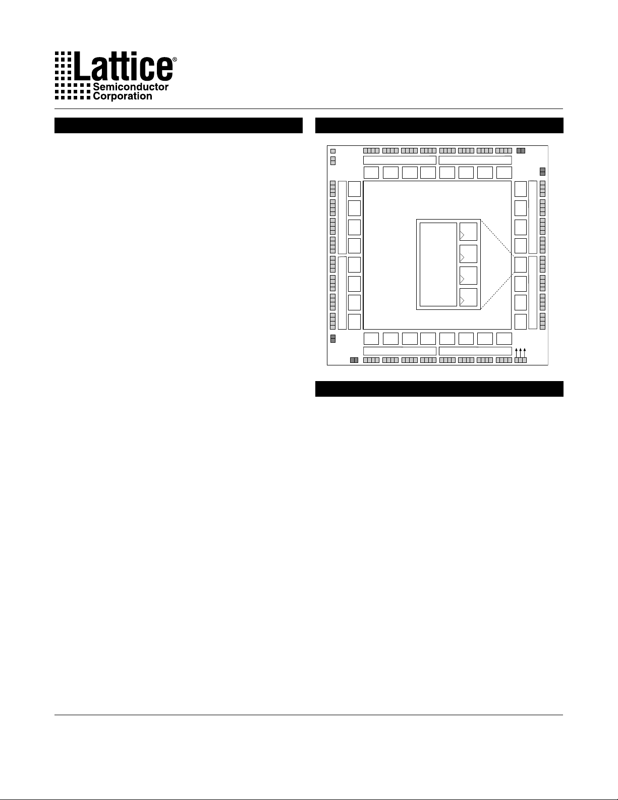
Functional Block Diagram*
Description
The ispLSI 2128VE is a High Density Programmable
Logic Device available in 128 and 64 I/O-pin versions.
The device contains 128 Registers, eight Dedicated
Input pins, three Dedicated Clock Input pins, two dedicated Global OE input pins and a Global Routing Pool
(GRP). The GRP provides complete interconnectivity
between all of these elements. The ispLSI 2128VE
features in-system programmability through the Boundary Scan Test Access Port (TAP) and is 100% IEEE
1149.1 Boundary Scan Testable. The ispLSI 2128VE
offers non-volatile reprogrammability of the logic, as well
as the interconnect to provide truly reconfigurable systems.
The basic unit of logic on the ispLSI 2128VE device is the
Generic Logic Block (GLB). The GLBs are labeled A0, A1
.. D7 (see Figure 1). There are a total of 32 GLBs in the
ispLSI 2128VE device. Each GLB is made up of four
macrocells. Each GLB has 18 inputs, a programmable
AND/OR/Exclusive OR array, and four outputs which can
be configured to be either combinatorial or registered.
Inputs to the GLB come from the GRP and dedicated
inputs. All of the GLB outputs are brought back into the
GRP so that they can be connected to the inputs of any
GLB on the device.
Page 2
Specifications ispLSI 2128VE
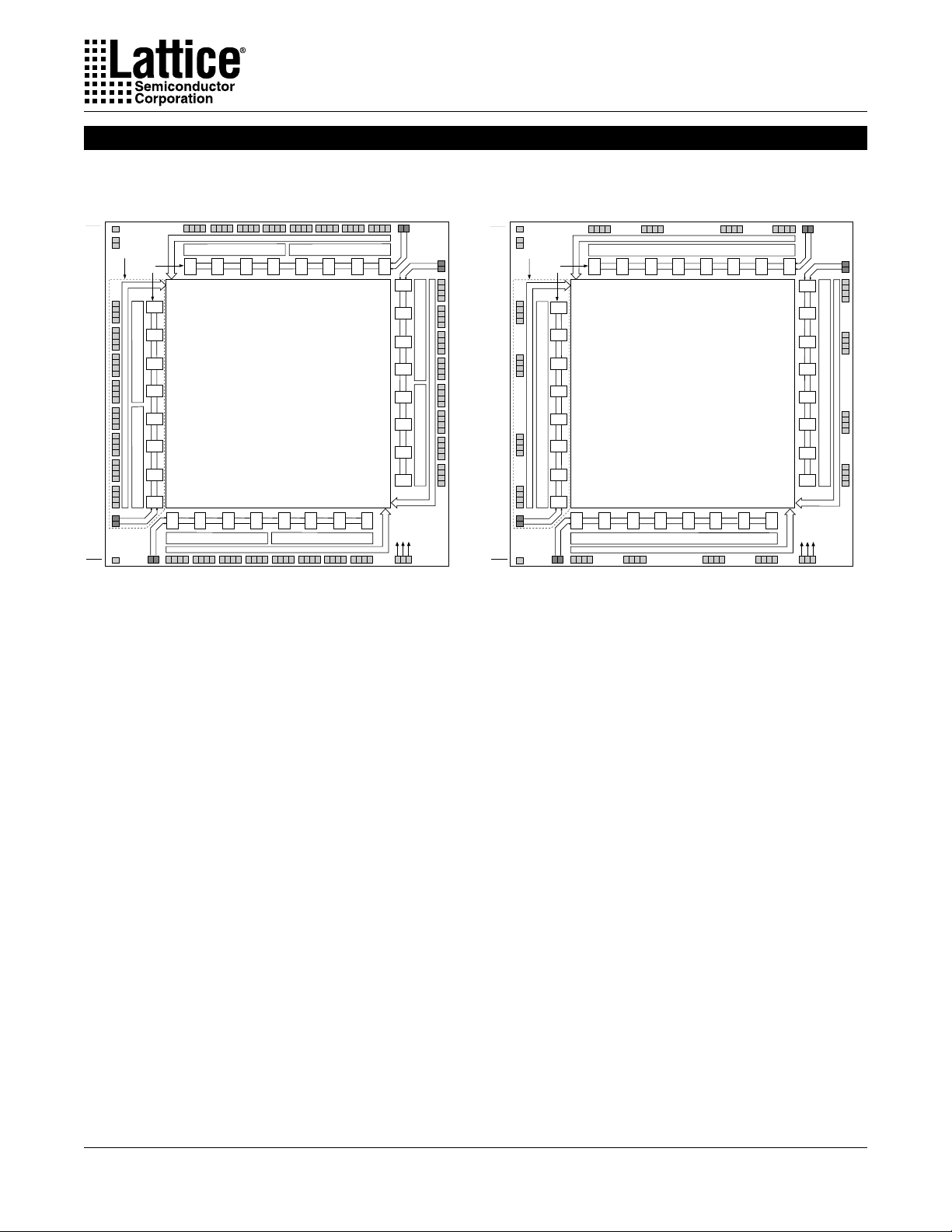
Functional Block Diagram
Figure 1. ispLSI 2128VE Functional Block Diagram (128-I/O and 64-I/O Versions)
I/O 127
I/O 126
I/O 125
I/O 124
I/O 123
I/O 122
I/O 121
I/O 120
I/O 119
I/O 118
I/O 117
I/O 116
I/O 115
I/O 114
I/O 113
I/O 112
I/O 111
I/O 110
I/O 109
I/O 108
I/O 107
I/O 106
I/O 105
I/O 104
I/O 103
I/O 102
I/O 101
I/O 100
I/O 99
I/O 98
I/O 97
I/O 96
IN 7
RESET
GOE 0
GOE 1
I/O 10
I/O 11
I/O 12
I/O 13
I/O 14
I/O 15
I/O 16
I/O 17
I/O 18
I/O 19
I/O 20
I/O 21
I/O 22
I/O 23
I/O 24
I/O 25
I/O 26
I/O 27
I/O 28
I/O 29
I/O 30
I/O 31
TDI/IN 0
TMS/IN 1
BSCAN
IN 6
I/O 42
I/O 43
Input Bus
D5
D4
Global
Routing
Pool
(GRP)
B3
Input Bus
I/O 44
I/O 45
I/O 46
I/O 47
I/O 48
D2
D3
B5
B4
I/O 49
I/O 50
I/O 51
I/O 52
I/O 53
I/O 54
I/O 55
I/O 56
I/O 57
D0
D1
C7
C6
C5
C4
Input Bus
C3
C2
C1
Output Routing Pool (ORP) Output Routing Pool (ORP)
C0
B7
B6
CLK 0
CLK 1
CLK 2
0139B/2128VE
I/O 60
I/O 61
I/O 62
I/O 63
Y0Y1Y2
I/O 58
I/O 59
Megablock
G
e
n
e
r
c
L
i
o
g
c
i
)
s
(
s
G
L
k
B
o
l
c
B
I/O 0
I/O 1
I/O 2
I/O 3
I/O 4
I/O 5
I/O 6
I/O 7
I/O 8
I/O 9
A0
A1
A2
A3
Input Bus
A4
A5
A6
Output Routing Pool (ORP) Output Routing Pool (ORP)
A7
TDO/IN 2
Output Routing Pool (ORP) Output Routing Pool (ORP)
D7
D6
B0
B1
B2
Output Routing Pool (ORP) Output Routing Pool (ORP)
I/O 32
I/O 33
I/O 34
I/O 35
I/O 36
I/O 37
I/O 38
I/O 39
I/O 40
TCK/IN 3
I/O 41
IN 5
IN 4
I/O 95
I/O 94
I/O 93
I/O 92
I/O 91
I/O 90
I/O 89
I/O 88
I/O 87
I/O 86
I/O 85
I/O 84
I/O 83
I/O 82
I/O 81
I/O 80
I/O 79
I/O 78
I/O 77
I/O 76
I/O 75
I/O 74
I/O 73
I/O 72
I/O 71
I/O 70
I/O 69
I/O 68
I/O 67
I/O 66
I/O 65
I/O 64
RESET
GOE 0
GOE 1
I/O 10
I/O 11
I/O 12
I/O 13
I/O 14
I/O 15
TDI/IN 0
TMS/IN 1
BSCAN
Megablock
G
e
n
e
r
i
k
o
s
l
c
B
I/O 0
I/O 1
I/O 2
I/O 3
I/O 4
I/O 5
I/O 6
I/O 7
Input Bus
I/O 8
I/O 9
Output Routing Pool (ORP)
I/O 63
I/O 62
I/O 61
I/O 60
I/O 59
I/O 58
c
L
o
g
c
i
D7
D6
B1
D5
B2
Output Routing Pool (ORP)
I/O 20
I/O 21
I/O 22
I/O 23
)
(
s
G
L
B
A0
A1
A2
A3
A4
A5
A6
A7
B0
I/O 16
I/O 17
I/O 18
I/O 19
TCK/IN 3
TDO/IN 2
I/O 57
I/O 56
Input Bus
Output Routing Pool (ORP)
D4
D3
Global
Routing
Pool
(GRP)
B3
B4
Input Bus
I/O 24
B5
I/O 25
I/O 26
I/O 55
I/O 27
I/O 54
D2
I/O 53
I/O 52
B6
I/O 51
I/O 50
I/O 49
I/O 48
IN 7*
IN 6*
D0
D1
C7
C6
C5
C4
C3
C2
C1
C0
B7
CLK 0
CLK 1
CLK 2
0139B/2128VE.64IO
Y0Y1Y2
I/O 28
I/O 29
I/O 30
I/O 31
*Not available on 84-PLCC Device
IN 5*
IN 4*
I/O 47
I/O 46
I/O 45
I/O 44
I/O 43
I/O 42
I/O 41
I/O 40
Input Bus
I/O 39
Output Routing Pool (ORP)
I/O 38
I/O 37
I/O 36
I/O 35
I/O 34
I/O 33
I/O 32
The 128-I/O 2128VE contains 128 I/O cells, while the 64I/O version contains 64 I/O cells. Each I/O cell is directly
connected to an I/O pin and can be individually programmed to be a combinatorial input, output or
bi-directional I/O pin with 3-state control. The signal
levels are TTL compatible voltages and the output drivers
can source 4mA or sink 8mA. Each output can be
programmed independently for fast or slow output slew
rate to minimize overall output switching noise. Device
pins can be safely driven to 5V signal levels to support
mixed-voltage systems.
Eight GLBs, 32 or 16 I/O cells, two dedicated inputs and
two or one ORPs are connected together to make a
Megablock (see Figure 1). The outputs of the eight GLBs
are connected to a set of 32 or 16 universal I/O cells by
the two or one ORPs. Each ispLSI 2128VE device
contains four Megablocks.
The GRP has as its inputs, the outputs from all of the
GLBs and all of the inputs from the bi-directional I/O cells.
All of these signals are made available to the inputs of the
GLBs. Delays through the GRP have been equalized to
minimize timing skew.
Y1, Y2) or an asynchronous clock can be selected on a
GLB basis. The asynchronous or Product Term clock
can be generated in any GLB for its own clock.
Programmable Open-Drain Outputs
In addition to the standard output configuration, the
outputs of the ispLSI 2128VE are individually programmable, either as a standard totem-pole output or an
open-drain output. The totem-pole output drives the
specified Voh and Vol levels, whereas the open-drain
output drives only the specified Vol. The Voh level on the
open-drain output depends on the external loading and
pull-up. This output configuration is controlled by a programmable fuse. The default configuration when the
device is in bulk erased state is totem-pole configuration.
The open-drain/totem-pole option is selectable through
the ispDesignEXPERT software tools.
Clocks in the ispLSI 2128VE device are selected using
the dedicated clock pins. Three dedicated clock pins (Y0,
2
Page 3
Specifications ispLSI 2128VE
Absolute Maximum Ratings
1
Supply Voltage Vcc.................................. -0.5 to +5.4V
Input Voltage Applied............................... -0.5 to +5.6V
Off-State Output Voltage Applied ............ -0.5 to +5.6V
Storage Temperature................................ -65 to 150°C
Case Temp. with Power Applied .............. -55 to 125°C
Max. Junction Temp. (TJ) with Power Applied ... 150°C
1. Stresses above those listed under the “Absolute Maximum Ratings” may cause permanent damage to the device. Functional
operation of the device at these or at any other conditions above those indicated in the operational sections of this specification
is not implied (while programming, follow the programming specifications).
DC Recommended Operating Condition
V
V
V
CC
IL
IH
SYMBOL
Supply Voltage
Input Low Voltage
Input High Voltage
PARAMETER
Commercial
Industrial
TA = 0°C to + 70°C
= -40°C to + 85°C
T
A
MIN. MAX. UNITS
3.0
3.0
V – 0.5
SS
2.0
3.6
3.6
0.8
5.25
Table 2-0005/2128VE
V
V
V
V
Capacitance (TA=25°C, f=1.0 MHz)
SYMBOL
C
1
C
2
C
3
I/O Capacitance
Clock and Global Output Enable Capacitance
PARAMETER
Erase Reprogram Specifications
PARAMETER MINIMUM MAXIMUM UNITS
Erase/Reprogram Cycles
UNITSTYPICAL TEST CONDITIONS
8Dedicated Input Capacitance
6
10
10,000 – Cycles
pf
pf
pf V = 3.3V, V = 0.0V
V = 3.3V, V = 0.0V
CC
V = 3.3V, V = 0.0V
CC I/O
CC Y
IN
Table 2-0006/2128VE
Table 2-0008/2128VE
3
Page 4
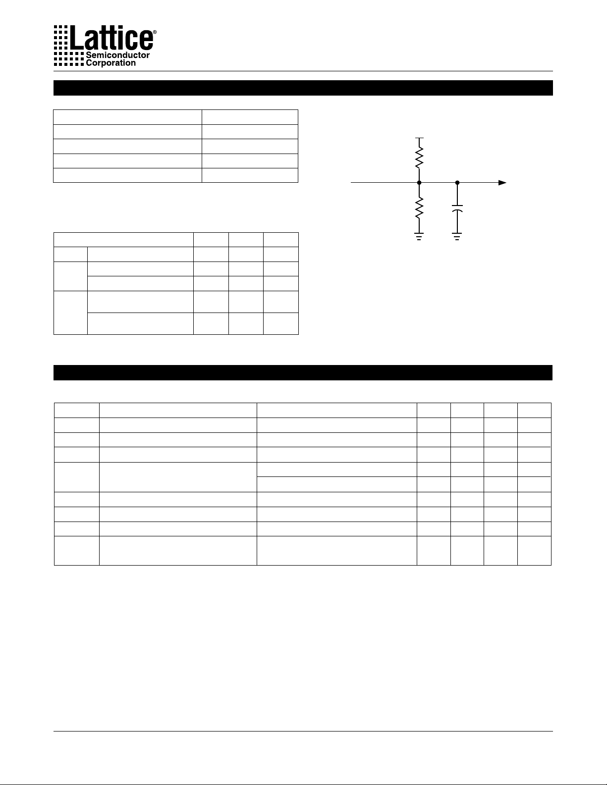
Switching Test Conditions
+ 3.3V
R
1
R
2
C
L
*
Device
Output
Test
Point
*
CL includes Test Fixture and Probe Capacitance.
0213A/2128VE
Specifications ispLSI 2128VE
Input Pulse Levels
Input Rise and Fall Time
Input Timing Reference Levels
Output Timing Reference Levels
Output Load
3-state levels are measured 0.5V from steady-state active level.
GND to 3.0V
≤ 1.5ns 10% to 90%
1.5V
1.5V
See Figure 2
Table 2 - 0003/2128VE
Figure 2. Test Load
Output Load Conditions (see Figure 2)
TEST CONDITION R1 R2 CL
A 316Ω 348Ω 35pF
∞
∞
348Ω 35pF
348Ω 5pF
Table 2-0004/2128VE
Active High
B
Active Low
Active High to Z
at V -0.5V
C
Active Low to Z
at V +0.5V
OH
OL
316Ω 348Ω 35pF
316Ω 348Ω 5pF
DC Electrical Characteristics
Over Recommended Operating Conditions
–
–
–
–
–
–
–
–
195
3
0.4
–
-10
10
10
-150
-150
-100
–
Table 2-0007/2128VE
µA
µA
µA
µA
µA
mA
mA
SYMBOL
V
OL
V
OH
I
IL
I
IH
I
IL-isp
I
IL-PU
I
OS
I
CC
Output Low Voltage
Output High Voltage
Input or I/O Low Leakage Current
Input or I/O High Leakage Current
BSCAN Input Low Leakage Current
I/O Active Pull-Up Current
1
Output Short Circuit Current
2, 4
Operating Power Supply Current
1. One output at a time for a maximum duration of one second. V = 0.5V was selected to avoid test
PARAMETER
CONDITION MIN. TYP. MAX. UNITS
I = 8 mA
OL
I = -4 mA
OH
0V ≤ V ≤ V (Max.)
IN IL
(V - 0.2)V ≤ V ≤ V
CC CC IN
V ≤ V ≤ 5.25V
IN
CC
0V ≤ V ≤ V
IN
IL
0V ≤ V ≤ V
IN IL
V = 3.3V, V = 0.5V
CC OUT
V = 0.0V, V = 3.0V
IL
f = 1 MHz
CLOCK
IH
OUT
–
2.4
–
–
–
–
–
–
–
problems by tester ground degradation. Characterized but not 100% tested.
2. Measured using eight 16-bit counters.
3. Typical values are at V = 3.3V and T = 25°C.
4. Maximum I varies widely with specific device configuration and operating frequency. Refer to the Power Consumption
CC
CC
A
section of this data sheet and Thermal Management section of the Lattice Semiconductor Data Book or CD-ROM to
estimate maximum I .
CC
V
V
4
Page 5

Specifications ispLSI 2128VE
External Timing Parameters
Over Recommended Operating Conditions
3
TEST
COND.
t
pd1
t
pd2
f
max
f
max (Ext.)
f
max (Tog.)
t
su1
t
co1
t
h1
t
su2
t
co2
t
h2
t
r1
t
rw1
t
ptoeen
t
ptoedis
t
goeen
t
goedis
t
wh
t
wl
1. Unless noted otherwise, all parameters use a GRP load of four, 20 PTXOR path, ORP and Y0 clock.
2. Standard 16-bit counter using GRP feedback.
3. Reference Switching Test Conditions section.
A 1 Data Propagation Delay, 4PT Bypass, ORP Bypass ns
A 2 Data Propagation Delay ns
A 3 Clock Frequency with Internal Feedback MHz
— 4 Clock Frequency with External Feedback MHz
— 5 Clock Frequency, Max. Toggle MHz
— 6 GLB Reg. Setup Time before Clock, 4 PT Bypass ns
A 7 GLB Reg. Clock to Output Delay, ORP Bypass ns
— 8 GLB Reg. Hold Time after Clock, 4 PT Bypass ns
— 9 GLB Reg. Setup Time before Clock ns
A 10 GLB Reg. Clock to Output Delay ns
— 11 GLB Reg. Hold Time after Clock ns
A 12 Ext. Reset Pin to Output Delay, ORP Bypass ns
— 13 Ext. Reset Pulse Duration ns
B 14 Input to Output Enable ns
C 15 Input to Output Disable ns
B 16 Global OE Output Enable ns
C 17 Global OE Output Disable ns
— 18 External Synchronous Clock Pulse Duration, High ns
— 19 External Synchronous Clock Pulse Duration, Low ns
DESCRIPTION#PARAMETER
1
2
1
( )
tsu2 + tco1
MIN. MAX.
— 4.0
—
250 —
158.7
275
2.5
—
0.0
3.3
—
0.0
—
3.5
—
—
—
—
1.8 —
1.8 —
-250
6.0
—
—
—
3.0
—
—
3.7
—
6.0
—
6.0
6.0
4.0
4.0
-180
MIN. MAX.
— 5.0
7.5
—
180 —
125
—
200
—
3.5
—
3.5
—
—
0.0
—
4.5
4.5
—
—
0.0
7.0
—
—
4.0
10.0
—
10.0
—
5.0
—
5.0
—
2.5 —
2.5 —
Table 2-0030A/2128VE
UNITS
v.1.0
5
Page 6
Specifications ispLSI 2128VE
External Timing Parameters
Over Recommended Operating Conditions
3
TEST
COND.
t
pd1
t
pd2
f
max
f
max (Ext.)
f
max (Tog.)
t
su1
t
co1
t
h1
t
su2
t
co2
t
h2
t
r1
t
rw1
t
ptoeen
t
ptoedis
t
goeen
t
goedis
t
wh
t
wl
1. Unless noted otherwise, all parameters use a GRP load of four, 20 PTXOR path, ORP and Y0 clock.
2. Standard 16-bit counter using GRP feedback.
3. Reference Switching Test Conditions section.
A 1 Data Propagation Delay, 4PT Bypass, ORP Bypass ns
A 2 Data Propagation Delay ns
A 3 Clock Frequency with Internal Feedback MHz
— 4 Clock Frequency with External Feedback MHz
— 5 Clock Frequency, Max. Toggle MHz
— 6 GLB Reg. Setup Time before Clock, 4 PT Bypass ns
A 7 GLB Reg. Clock to Output Delay, ORP Bypass ns
— 8 GLB Reg. Hold Time after Clock, 4 PT Bypass ns
— 9 GLB Reg. Setup Time before Clock ns
A 10 GLB Reg. Clock to Output Delay ns
— 11 GLB Reg. Hold Time after Clock ns
A 12 Ext. Reset Pin to Output Delay, ORP Bypass ns
— 13 Ext. Reset Pulse Duration ns
B 14 Input to Output Enable ns
C 15 Input to Output Disable ns
B 16 Global OE Output Enable ns
C 17 Global OE Output Disable ns
— 18 External Synchronous Clock Pulse Duration, High ns
— 19 External Synchronous Clock Pulse Duration, Low ns
DESCRIPTION#PARAMETER
1
2
1
( )
tsu2 + tco1
MIN.
— 7.5 — 10.0
——
135 — 100 —
100
143
5.0
——
0.0 —
6.0 —
——
0.0 —
——
5.0 —
——
——
——
——
3.5 ——
3.5 ——
-135
10.0
4.0
5.0
9.0
12.0
12.0
7.0
7.0
-100
MIN.MAX. MAX.
13.0
77
——
100
——
6.5
——
5.0
0.0
—
8.0
—
6.0
—
0.0
12.5
—
6.5
15.0
15.0
9.0
9.0
5.0
5.0
Table 2-0030B/2128VE
UNITS
v.1.0
6
Page 7

Specifications ispLSI 2128VE
Internal Timing Parameters
1
Over Recommended Operating Conditions
PARAMETER
Inputs
t
io
t
din
GRP
t
grp
GLB
t
4ptbpc
t
4ptbpr
t
1ptxor
t
20ptxor
t
xoradj
t
gbp
t
gsu
t
gh
t
gco
t
gro
t
ptre
t
ptoe
t
ptck
ORP
t
orp
t
orpbp
Outputs
t
ob
t
sl
t
oen
t
odis
t
goe
Clocks
t
gy0
t
gy1/2
Global Reset
t
gr
1. Internal Timing Parameters are not tested and are for reference only.
2. Refer to Timing Model in this data sheet for further details.
3. The XOR adjacent path can only be used by hard macros.
2
20 Input Buffer Delay ns
21 Dedicated Input Delay ns
22 GRP Delay ns
23 4 Product Term Bypass Path Delay (Combinatorial) ns
24 4 Product Term Bypass Path Delay (Registered) ns
25 1 Product Term/XOR Path Delay ns
26 20 Product Term/XOR Path Delay ns
27 XOR Adjacent Path Delay ns
28 GLB Register Bypass Delay ns
29 GLB Register Setup Time before Clock ns
30 GLB Register Hold Time after Clock ns
31 GLB Register Clock to Output Delay ns
32 GLB Register Reset to Output Delay ns
33 GLB Product Term Reset to Register Delay ns
34 GLB Product Term Output Enable to I/O Cell Delay ns
35 GLB Product Term Clock Delay ns
36 ORP Delay ns
37 ORP Bypass Delay ns
38 Output Buffer Delay ns
39 Output Slew Limited Delay Adder ns
40 I/O Cell OE to Output Enabled ns
41 I/O Cell OE to Output Disabled ns
42 Global Output Enable ns
43 Clock Delay, Y0 to Global GLB Clock Line (Ref. clock) ns
44 Clock Delay, Y1 or Y2 to Global GLB Clock Line ns
45 Global Reset to GLB
DESCRIPTION#
3
-250
MIN. MAX.
0.5
—
0.7
—
0.2
—
1.5
—
2.0
—
2.8
—
2.8
—
2.8
—
0.0
—
—
0.8
—
1.7
0.2
—
0.3
—
3.7
—
2.9
—
3.6
0.8
1.1
—
0.4
—
1.4
—
2.0
—
2.4
—
2.4
—
1.6
—
1.0
1.0
1.2
1.2
3.9
— ns
-180
MIN. MAX.
0.5
—
1.1
—
0.6
—
1.9
—
2.4
—
3.4
—
3.4
—
3.4
—
0.0
—
—
1.2
—
2.3
0.3
—
0.6
—
4.3
—
5.9
—
4.0
1.0
1.4
—
0.4
—
1.6
—
2.0
—
3.0
—
3.0
—
2.0
—
1.2
1.2
1.4
1.4
4.4
—
Table 2-0036A/2128VE
v.1.0
UNITS
7
Page 8

Specifications ispLSI 2128VE
Internal Timing Parameters
1
Over Recommended Operating Conditions
PARAMETER
Inputs
tio
tdin
GRP
tgrp
GLB
t4ptbpc
t4ptbpr
t1ptxor
t20ptxor
txoradj
tgbp
tgsu
tgh
tgco
tgro
tptre
tptoe
tptck
ORP
torp
torpbp
Outputs
tob
tsl
toen
todis
tgoe
Clocks
tgy0
tgy1/2
Global Reset
tgr
1. Internal Timing Parameters are not tested and are for reference only.
2. Refer to Timing Model in this data sheet for further details.
3. The XOR adjacent path can only be used by hard macros.
2
20 Input Buffer Delay ns
21 Dedicated Input Delay ns
22 GRP Delay ns
23 4 Product Term Bypass Path Delay (Combinatorial) ns
24 4 Product Term Bypass Path Delay (Registered) ns
25 1 Product Term/XOR Path Delay ns
26 20 Product Term/XOR Path Delay ns
27 XOR Adjacent Path Delay ns
28 GLB Register Bypass Delay ns
29 GLB Register Setup Time before Clock ns
30 GLB Register Hold Time after Clock ns
31 GLB Register Clock to Output Delay ns
32 GLB Register Reset to Output Delay ns
33 GLB Product Term Reset to Register Delay ns
34 GLB Product Term Output Enable to I/O Cell Delay ns
35 GLB Product Term Clock Delay ns
36 ORP Delay ns
37 ORP Bypass Delay ns
38 Output Buffer Delay ns
39 Output Slew Limited Delay Adder ns
40 I/O Cell OE to Output Enabled ns
41 I/O Cell OE to Output Disabled ns
42 Global Output Enable ns
43 Clock Delay, Y0 to Global GLB Clock Line (Ref. clock) ns
44 Clock Delay, Y1 or Y2 to Global GLB Clock Line ns
45 Global Reset to GLB ns
DESCRIPTION#
3
MIN.
—
—
—
—
—
—
—
—
—
1.2
3.8
—
—
—
—
1.6
—
—
—
—
—
—
—
1.6
1.8
—
-135
0.5
1.7
1.2
3.7
3.7
4.7
4.7
4.7
0.5
—
—
0.3
1.1
6.1
6.9
4.6
1.5
0.5
1.6
2.0
3.4
3.4
3.6
1.6
1.8
5.8
-100
MIN.MAX. MAX.
—
0.7
—
2.5
—
1.8
—
5.2
—
4.7
—
6.2
—
6.2
—
6.2
—
1.0
1.7
4.8
2.6
2.4
2.6
—
—
—
0.3
—
3.1
—
7.1
—
9.1
5.6
—
1.7
—
0.7
—
1.6
—
2.0
—
3.4
—
3.4
—
5.6
2.4
2.6
—
7.1
Table 2-0036B/2128VE
UNITS
v.1.0
8
Page 9

ispLSI 2128VE Timing Model
Specifications ispLSI 2128VE
I/O CellORPGLBGRPI/O Cell
Feedback
Ded. In
I/O Pin
(Input)
Reset
Y0,1,2
GOE 0
#21
I/O Delay
#20
#45
#43, 44
GRP
#22
#42
Reg 4 PT Bypass
Comb 4 PT Bypass #23
#24
20 PT
XOR Delays
#25, 26, 27
Control
RE
PTs
OE
CK
#33, 34,
35
Derivations of tsu, th and tco from the Product Term Clock
2.5ns
=
Logic + Reg su - Clock (min)
t
io + tgrp + t20ptxor) + (tgsu) - (tio + tgrp + tptck(min))
=
(
(#20 + #22 + #26) + (#29) - (#20 + #22 + #35)
=
(0.5 + 0.2 + 2.8) + (0.8) - (0.5 + 0.2 + 0.8)
=
=
t
io + tgrp + tptck(max)) + (tgh) - (tio + tgrp + t20ptxor)
(
=
(#20 + #22 + #35) + (#30) - (#20 + #22 + #26)
=
(0.5 + 0.2 + 3.6) + (1.7) - (0.5 + 0.2 + 2.8)
=
t
su
2.8ns
t
h Clock (max) + Reg h - Logic
GLB Reg Bypass ORP Bypass
#28
GLB Reg
Delay
DQ
RST
#29, 30,
31, 32
#37
ORP
Delay
#36
#38,
#40, 41
0491/2032
39
I/O Pin
(Output)
7.0ns
=
Clock (max) + Reg co + Output
t
io + tgrp + tptck(max)) + (tgco) + (torp + tob)
=
(
(#20 + #22 + #35) + (#31) + (#36 + #38)
=
(0.5 + 0.2 + 3.6) + (0.2) + (1.1 + 1.4)
=
t
co
Note: Calculations are based upon timing specifications for the ispLSI 2128VE-250L.
Table 2-0042/2128VE
v.1.0
9
Page 10

Power Consumption
Specifications ispLSI 2128VE
Power consumption in the ispLSI 2128VE device depends on two primary factors: the speed at which the
device is operating and the number of Product Terms
Figure 3. Typical Device Power Consumption vs fmax
350
300
250
200
CC (mA)
I
150
100
0 50 100 150 200 250
f
max (MHz)
Notes: Configuration of eight 16-bit counters
Typical current at 3.3V, 25¡ C
used. Figure 3 shows the relationship between power
and operating speed.
ispLSI 2128VE
I
can be estimated for the ispLSI 2128VE using the following equation:
CC
ICC =
8 + (# of PTs * 0.669) + (# of nets * max freq * 0.0026)
Where:
# of PTs = Number of Product Terms used in design
# of nets = Number of Signals used in device
Max freq = Highest Clock Frequency to the device (in MHz)
The
I
estimate is based on typical conditions (VCC = 3.3V, room temperature) and an assumption
CC
of two GLB loads on average exists. These values are for estimates only. Since the value of
sensitive to operating conditions and the program in the device, the actual
I
should be verified.
CC
I
is
CC
0127/2128VE
10
Page 11

Specifications ispLSI 2128VE
Signal Descriptions
Signal Name Description
RESET Active Low (0) Reset pin resets all the registers in the device.
GOE 0, GOE1 Global Output Enable input pins.
Y0, Y1, Y2 Dedicated Clock Input – These clock inputs are connected to one of the clock inputs of all the GLBs in
the device.
BSCAN Input – Dedicated in-system programming Boundary Scan enable input pin. This pin is brought low to
enable the programming mode. The TMS, TDI, TDO and TCK controls become active.
TDI/IN 0 Input – This pin performs two functions. When BSCAN is logic low, it functions as a serial data input pin
to load programming data into the device. When BSCAN is high, it functions as a dedicated input pin.
TCK/IN 3 Input – This pin performs two functions. When BSCAN is logic low, it functions as a clock pin for the
Boundary Scan state machine. When BSCAN is high, it functions as a dedicated input pin.
TMS/IN 1 Input – This pin performs two functions. When BSCAN is logic low, it functions as a mode control pin for
the Boundary Scan state machine. When BSCAN is high, it functions as a dedicated input pin.
TDO/IN 2 Output/Input – This pin performs two functions. When BSCAN is logic low, it functions as an output pin
to read serial shift register data. When BSCAN is high, it functions as a dedicated input pin.
IN 4 - IN 7 Dedicated Input Pins to the device.
GND Ground (GND)
VCC Vcc
1
NC
I/O Input/Output Pins – These are the general purpose I/O pins used by the logic array.
1. NC pins are not to be connected to any active signals, VCC or GND.
No Connect
11
Page 12

Signal Locations
Specifications ispLSI 2128VE
llaB-802
langiS
TESER
2Y,1Y,0Y41J,41H,2H801,311,0289,301,818F,6F,3E06,56,01
NACSB
0NI/IDT3J62422F61
3NI/KCT51J7017901G95
1NI/SMT8P66065J73
2NI/ODT9C4510416B78
7NI-4NI,8T,9A,61H
DNG,7G,31D,4D
CCV,21D,6D,5D
1
CN
3H12912D11
1EOG,0EOG1H,61J32,01112,0011E,9F31,26
1J52325E51
4H
AGBpfAGBpf
AGBpfAGBpf
AGBpf
91
,01G,9G,8G
,9H,8H,7H
,8J,7J,01H
,7K,01J,9J
,01K,9K,8K
31N,4N
,4F,31E,4E
21N,11N
,51A,3A,2A
,2B,1B,61A
,3C,2C,61B
,3P,2P,1P
,3R,2R,1R
,51T,2T,1T
61T
571
,31L,4L,31F
651
,5N,31M,4M
,51B,41B,3B
,41D,51C,41C
,51P,41P,31P
,61R,51R,41R
niP-671
PFQTPFQT
PFQTPFQT
PFQT
,76,551,411
71
,78,86,64,42
,351,431,901
951
,56,34,22,2
,131,111,09
241
,63,72,81,9
,211,601,79
661,751,251
201,4C,3C,8A
,87,96,46,55
,341,421,511
niP-061
PFQPPFQP
PFQPPFQP
PFQP
,16,141,401
,97,26,24,22
,931,221,99
,95,93,02,2
,911,101,28
.DNGroCCV,slangisevitcaynaotdetcennocebottonerasnipCN.1
AGBacAGBac
AGBacAGBac
AGBac
,7E,8D,6D
llaB-001
,3G,4F,01E
1D,5K,6A,9E9,83,88,66
6K,9G,1F,7B68,16,93,41
4J,01F,2E,5A98,36,63,21
3K,8H,7H,5G
niP-001
PFQTPFQT
PFQTPFQT
PFQT
,13,52,12,4
,46,45,05,44
,49,18,57,17
001
12
Page 13

I/O Locations
Specifications ispLSI 2128VE
Signal fpBGA TQFP PQFP caBGA TQFP
208 176 160 100 100
I/O 0 J2 28 25 G1 17
I/O 1 J4 29 26 F3 18
I/O 2K13027E419
I/O 3 K3 31 28 H1 20
I/O 4 K2 32 29 G2 22
I/O 5 K4 33 30 J1 23
I/O 6L13431H224
I/O 7L23532K126
I/O 8L33733J227
I/O 9 M1 38 34 K2 28
I/O 10 M2 39 35 H3 29
I/O 11 M3 40 36 J3 30
I/O 12 N1 41 37 G4 32
I/O 13 N2 42 38 H4 33
I/O 14 N3 44 40 K4 34
I/O 15 P4 45 41 H5 35
I/O 16 T3 47 43 F5 40
I/O 17 R4 48 44 J6 41
I/O 18 T4 49 45 K7 42
I/O 19 P5 50 46 H6 43
I/O 20 R5 51 47 K8 45
I/O 21 N6 52 48 G6 46
I/O 22 T5 53 49 J7 47
I/O 23 R6 54 50 K9 48
I/O 24 P6 56 51 J8 49
I/O 25 T6 57 52 K10 51
I/O 26 N7 58 53 J9 52
I/O 27 R7 59 54 J10 53
I/O 28 P7 60 55 H9 55
I/O 29 T7 61 56 H10 56
I/O 30 N8 62 57 G7 57
I/O 31 R8 63 58 G8 58
I/O 32 T9 70 63 D10 67
I/O 33 P9 71 64 E8 68
I/O 34 R9 72 65 F7 69
I/O 35 N9 73 66 C10 70
I/O 36 T10 74 67 D9 72
I/O 37 P10 75 68 B10 73
I/O 38 R10 76 69 C9 74
I/O 39 N10 77 70 A10 76
I/O 40 T11 79 71 B9 77
I/O 41 P11 80 72 A9 78
I/O 42 R11 81 73 C8 79
I/O 43 T12 82 74 B8 80
I/O 44 P12 83 75 D7 82
I/O 45 R12 84 76 C7 83
I/O 46 T13 85 77 A7 84
I/O 47 R13 86 78 C6 85
I/O 48 T14 88 80 E6 90
I/O 49 N14 89 81 B5 91
I/O 50 P16 91 83 A4 92
I/O 51 N15 92 84 C5 93
I/O 52 N16 93 85 A3 95
I/O 53 M14 94 86 D5 96
I/O 54 M15 95 87 B4 97
I/O 55 M16 96 88 A2 98
I/O 56 L15 98 89 B3 99
I/O 57 L14 99 90 A1 1
I/O 58 L16 100 91 B2 2
I/O 59 K13 101 92 B1 3
I/O 60 K15 102 93 C2 5
I/O 61 K14 103 94 C1 6
I/O 62 K16 104 95 D4 7
I/O 63 J13 105 96 D3 8
Signal fpBGA TQFP PQFP caBGA TQFP
208 176 160 100 100
I/O 64 H15 116 105 ——
I/O 65 H13 117 106 ——
I/O 66 G16 118 107 ——
I/O 67 G14 119 108 ——
I/O 68 G15 120 109 ——
I/O 69 G13 121 110 ——
I/O 70 F16 122 111 ——
I/O 71 F14 123 112 ——
I/O 72 F15 125 113 ——
I/O 73 E16 126 114 ——
I/O 74 E14 127 115 ——
I/O 75 E15 128 116 ——
I/O 76 D16 129 117 ——
I/O 77 C16 130 118 ——
I/O 78 D15 132 120 ——
I/O 79 A14 133 121 ——
I/O 80 C13 135 123 ——
I/O 81 B13 136 124 ——
I/O 82 A13 137 125 ——
I/O 83 C12 138 126 ——
I/O 84 B12 139 127 ——
I/O 85 D11 140 128 ——
I/O 86 A12 141 129 ——
I/O 87 C11 142 130 ——
I/O 88 B11 144 131 ——
I/O 89 D10 145 132 ——
I/O 90 A11 146 133 ——
I/O 91 B10 147 134 ——
I/O 92 C10 148 135 ——
I/O 93 D9 149 136 ——
I/O 94 A10 150 137 ——
I/O 95 B9 151 138 ——
I/O 96 A8 158 143 ——
I/O 97 C8 159 144 ——
I/O 98 B8 160 145 ——
I/O 99 D8 161 146 ——
I/O 100 A7 162 147 ——
I/O 101 C7 163 148 ——
I/O 102 B7 164 149 ——
I/O 103 D7 165 150 ——
I/O 104 A6 167 151 ——
I/O 105 C6 168 152 ——
I/O 106 B6 169 153 ——
I/O 107 A5 170 154 ——
I/O 108 C5 171 155 ——
I/O 109 B5 172 156 ——
I/O 110 A4 173 157 ——
I/O 111 B4 174 158 ——
I/O 112 C4 176 160 ——
I/O 113 A1 1 1 ——
I/O 114 C1 3 3 ——
I/O 115 D3 4 4 ——
I/O 116 D2 5 5 ——
I/O 117 D1 6 6 ——
I/O 118 E3 7 7 ——
I/O 119 E2 8 8 ——
I/O 120 E1 10 9 ——
I/O 121 F3 11 10 ——
I/O 122 F2 12 11 ——
I/O 123 F1 13 12 ——
I/O 124 G4 14 13 ——
I/O 125 G2 15 14 ——
I/O 126 G3 16 15 ——
I/O 127 G1 17 16 ——
13
Page 14

Signal Configuration
ispLSI 2128VE 208-Ball fpBGA Signal Diagram
I/O79I/O82I/O86I/O90I/O
A
B
NC1NC
NC
1
I/O
I/O
I/O
1
1
1
NC
NC
81
84
88
94
I/O
91
IN 5
I/O
95
Specifications ispLSI 2128VE
12345678910111213141516
I/O
I/O
I/O96I/O
100
I/O
I/O
102
98
104
I/O
106
107
I/O
109
I/O
110
I/O
111
NC1NC
1
NC
NC
I/O
1
1
113
NC
A
1
B
I/O
C
77
I/O
D
76
I/O73I/O75I/O
E
I/O70I/O72I/O
F
I/O66I/O
G
IN 4
H
GOE0TCK/
J
I/O
K
62
I/O58I/O56I/O
L
I/O55I/O54I/O
M
I/O52I/O51I/O
N
NC
74
71
1
1
GND
VCC
VCC
NC1NC
I/O
78
I/O67I/O
68
I/O
Y1
64
IN 3
Y2
I/O60I/O61I/O
VCC
57
VCC
53
49
I/O80I/O83I/O
87
VCC
I/O
85
69
I/O
65
I/O
63
59
I/O
92
I/O
89
TDO/
IN 2
I/O
93
I/O
97
I/O
99
I/O
101
I/O
103
GND GND GND GND
GND GND GND GND
GND GND GND GND
GND GND GND GND
ispLSI 2128VE
Bottom View
I/O39I/O35I/O30I/O26I/O
I/O
105
VCC
21
I/O
I/O
108
112
GNDVCC
VCC
VCC
I/O
124
IN 7 Y0
I/O1TDI/
I/O
5
VCC
VCC
GNDVCCVCCVCCGND
NC
I/O
115
I/O
118
I/O
121
I/O
126
RESET
IN 0
I/O
3
I/O
8
I/O
11
I/O
14
1
NC
I/O
116
I/O
119
I/O
122
I/O
125
I/O
BSCAN
0
I/O
4
I/O
7
I/O
10
I/O
13
114
I/O
117
I/O
120
I/O
123
I/O
127
GOE
1
I/O
2
I/O
6
I/O
9
I/O
12
C
D
E
F
G
H
J
K
L
M
N
I/O
1
I/O
P
50
R
NC1NC1NC
T
NC1NC
NC
1
1
1
NC
NC
1
I/O48I/O46I/O43I/O40I/O36I/O
I/O
1
I/O41I/O37I/O33TMS/
44
I/O47I/O45I/O42I/O38I/O34I/O31I/O27I/O23I/O20I/O
32
1. NCs are not to be connected to any active signals, Vcc or GND.
Note: Ball A1 indicator dot on top side of package.
14
IN 1
IN 6
I/O28I/O
24
I/O19I/O
15
17
I/O29I/O25I/O22I/O
18
NC1NC1NC
NC1NC1NC
I/O
NC1NC
16
12345678910111213141516
208 BGA/2128VE
1
P
1
R
1
T
Page 15

Pin Configuration
ispLSI 2128VE 176-Pin TQFP Pinout Diagram
I/O 112
GND
I/O 111
I/O 110
I/O 109
I/O 108
I/O 107
I/O 106
I/O 105
I/O 104
NC1I/O 103
I/O 102
I/O 101
I/O 100
176
175
174
173
172
171
170
169
168
167
166
165
164
163
162
VCC
1
NC
1
NC
IN 7
VCC
1
NC
I/O 0
I/O 1
I/O 2
I/O 3
I/O 4
I/O 5
I/O 6
I/O 7
1
NC
I/O 8
I/O 9
VCC
1
2
3
4
5
6
7
8
9
10
11
12
13
14
15
16
17
18
19
20
Y0
21
22
23
24
25
26
27
28
29
30
31
32
33
34
35
36
37
38
39
40
41
42
43
44
45464748495051525354555657585960616263646566676869707172737475767778798081828384858687
ispLSI 2128VE
I/O 113
I/O 114
I/O 115
I/O 116
I/O 117
I/O 118
I/O 119
I/O 120
I/O 121
I/O 122
I/O 123
I/O 124
I/O 125
I/O 126
I/O 127
RESET
GOE 1
GND
BSCAN
TDI/IN 0
I/O 10
I/O 11
I/O 12
I/O 13
I/O 14
I/O 99
I/O 98
I/O 97
I/O 96
NC1VCC
161
160
159
158
157
Top View
Specifications ispLSI 2128VE
IN 5
TDO/IN 2
GND
NC1I/O 95
I/O 94
I/O 93
I/O 92
I/O 91
I/O 90
I/O 89
I/O 88
NC1I/O 87
I/O 86
I/O 85
I/O 84
I/O 83
I/O 82
I/O 81
I/O 80
GND
I/O 79
156
155
154
153
152
151
150
149
148
147
146
145
144
143
142
141
140
139
138
137
136
135
134
133
88
132
131
130
129
128
127
126
125
124
123
122
121
120
119
118
117
116
115
114
113
112
111
110
109
108
107
106
105
104
103
102
101
100
I/O 78
VCC
I/O 77
I/O 76
I/O 75
I/O 74
I/O 73
I/O 72
NC
I/O 71
I/O 70
I/O 69
I/O 68
I/O 67
I/O 66
I/O 65
I/O 64
NC
IN 4
Y1
NC
VCC
GOE 0
GND
Y2
TCK/IN 3
NC
I/O 63
I/O 62
I/O 61
I/O 60
I/O 59
I/O 58
I/O 57
99
I/O 56
98
NC
97
I/O 55
96
I/O 54
95
I/O 53
94
I/O 52
93
I/O 51
92
I/O 50
91
VCC
90
I/O 49
89
1
1
1
1
1
GND
I/O 15
I/O 16
I/O 17
I/O 18
I/O 19
I/O 20
I/O 21
I/O 22
1
I/O 23
NC
I/O 24
I/O 25
I/O 26
I/O 27
I/O 28
I/O 29
I/O 30
1
NC
I/O 31
VCC
TMS/IN 1
IN 6
GND
1
NC
I/O 32
I/O 33
I/O 34
I/O 35
I/O 36
I/O 37
I/O 38
I/O 39
1
NC
I/O 40
I/O 41
1. NC pins are not to be connected to any active signals, VCC or GND.
15
I/O 42
I/O 43
I/O 44
I/O 45
I/O 46
GND
I/O 47
I/O 48
176-TQFP/2128VE
Page 16

Pin Configuration
ispLSI 2128VE 160-Pin PQFP Pinout Diagram
I/O 112
GND
I/O 111
I/O 110
I/O 109
I/O 108
I/O 107
I/O 106
I/O 105
I/O 104
I/O 103
I/O 102
I/O 101
I/O 100
160
159
158
157
156
155
154
153
152
151
150
149
148
147
VCC
IN 7
VCC
I/O 0
I/O 1
I/O 2
I/O 3
I/O 4
I/O 5
I/O 6
I/O 7
I/O 8
I/O 9
VCC
1
2
3
4
5
6
7
8
9
10
11
12
13
14
15
16
17
18
Y0
19
20
21
22
23
24
25
26
27
28
29
30
31
32
33
34
35
36
37
38
39
40
ispLSI 2128VE
I/O 113
I/O 114
I/O 115
I/O 116
I/O 117
I/O 118
I/O 119
I/O 120
I/O 121
I/O 122
I/O 123
I/O 124
I/O 125
I/O 126
I/O 127
RESET
GOE 1
GND
BSCAN
TDI/IN 0
I/O 10
I/O 11
I/O 12
I/O 13
I/O 14
I/O 99
I/O 98
I/O 97
I/O 96
VCC
IN 5
146
145
144
143
142
141
Top View
Specifications ispLSI 2128VE
TDO/IN 2
GND
I/O 95
I/O 94
I/O 93
I/O 92
I/O 91
I/O 90
I/O 89
I/O 88
I/O 87
I/O 86
I/O 85
I/O 84
I/O 83
I/O 82
I/O 81
I/O 80
GND
I/O 79
140
139
138
137
136
135
134
133
132
131
130
129
128
127
126
125
124
123
122
121
120
I/O 78
119
VCC
118
I/O 77
117
I/O 76
116
I/O 75
115
I/O 74
114
I/O 73
113
I/O 72
112
I/O 71
111
I/O 70
110
I/O 69
109
I/O 68
108
I/O 67
107
I/O 66
106
I/O 65
105
I/O 64
104
IN 4
103
Y1
102
101
100
99
98
97
96
95
94
93
92
91
90
89
88
87
86
85
84
83
82
81
1
NC
VCC
GOE 0
GND
Y2
TCK/IN 3
I/O 63
I/O 62
I/O 61
I/O 60
I/O 59
I/O 58
I/O 57
I/O 56
I/O 55
I/O 54
I/O 53
I/O 52
I/O 51
I/O 50
VCC
I/O 49
414243444546474849505152535455565758596061626364656667686970717273747576777879
IN 6
GND
I/O 15
I/O 16
I/O 17
I/O 18
I/O 19
I/O 20
I/O 21
I/O 22
I/O 23
I/O 24
I/O 25
I/O 26
I/O 27
I/O 28
I/O 29
I/O 30
I/O 31
VCC
TMS/IN 1
GND
I/O 32
I/O 34
I/O 34
I/O 35
I/O 36
I/O 37
1. NC pins are not to be connected to any active signal, VCC or GND.
16
I/O 38
I/O 39
I/O 40
I/O 41
I/O 42
I/O 43
I/O 44
I/O 45
80
GND
I/O 46
I/O 47
I/O 48
160-PQFP/2128VE
Page 17

Signal Configuration
ispLSI 2128VE 100-Ball caBGA Signal Diagram
10987654321
Specifications ispLSI 2128VE
A
B
C
D
E
F
G
H
J
I/O
39
I/O
37
I/O
35
I/O
32
NC
VCC Y2 Y1
TCK/
IN 3
I/O
29
I/O
27
I/O
41
I/O
40
I/O
38
I/O
36
1
GOE
GND NC
I/O
28
I/O
26
NC
I/O
43
I/O
42
NC
I/O
33
0
I/O
31
NC
I/O
24
I/O
1
46
GND
I/O
45
I/O
1
44
I/O
34
I/O
30
1
NC
I/O
22
IN 5 VCC
TDO/
IN 2
1
1
I/O
47
I/O
48
I/O
21
I/O
19
I/O
17
I/O
50
I/O
49
I/O
51
I/O
1
53
BSCAN
I/O
16
NC
I/O
15
TMS/
IN 1
I/O
54
NC
I/O
62
I/O
2
NC
I/O
1
12
I/O
13
VCC
I/O
52
I/O
56
1
NC
I/O
63
I/O
1
1
I/O
10
I/O
11
I/O
55
I/O
58
I/O
1
60
RESET
VCCY0IN 4 NC
TDI/
IN 0
I/O
1
4
I/O
6
I/O
8
I/O
57
I/O
59
I/O
61
IN 7NC
GOE
1
GND
I/O
0
I/O
3
I/O
5
A
B
C
D
E
F
G
H
J
K
I/O
25
I/O
23
I/O
20
I/O
18
GND NC
IN 6
ispLSI 2128VE
Bottom View
10987654321
1
NCs are not to be connected to any active signals, VCC or GND.
Note: Ball A1 indicator dot on top side of package.
17
I/O
14
I/O
1
9
I/O
7
K
100-BGA/2128VE
Page 18

Pin Configuration
ispLSI 2128VE 100-Pin TQFP Pinout Diagram
NC1I/O 56
I/O 55
I/O 54
I/O 53
I/O 52
NC1I/O 51
I/O 50
I/O 49
Specifications ispLSI 2128VE
I/O 48
VCC
IN 5
TDO/IN 2
GND
I/O 47
I/O 46
I/O 45
I/O 44
NC1I/O 43
I/O 42
I/O 41
I/O 40
I/O 39
I/O 57
I/O 58
I/O 59
1
NC
I/O 60
I/O 61
I/O 62
I/O 63
IN 7
Y0
RESET
VCC
GOE 1
GND
BSCAN
TDI/IN 0
I/O 0
I/O 1
I/O 2
I/O 3
1
NC
I/O 4
I/O 5
I/O 6
1
NC
9998979695949392919089888786858483828180797877
100
1
2
3
4
5
6
7
8
9
10
11
12
ispLSI 2128VE
13
14
15
Top View
16
17
18
19
20
21
22
23
24
25
26272829303132333435363738394041424344454647484950
76
75
74
73
72
71
70
69
68
67
66
65
64
63
62
61
60
59
58
57
56
55
54
53
52
51
1
NC
I/O 38
I/O 37
I/O 36
1
NC
I/O 35
I/O 34
I/O 33
I/O 32
IN 4
Y1
1
NC
VCC
GOE 0
GND
Y2
TCK/IN 3
I/O 31
I/O 30
I/O 29
I/O 28
1
NC
I/O 27
I/O 26
I/O 25
I/O 7
I/O 8
I/O 9
I/O 10
NC
1
I/O 11
I/O 12
I/O 13
I/O 14
I/O 15
VCC
IN 6
GND
I/O 16
I/O 17
1
I/O 18
I/O 19
NC
I/O 20
I/O 21
I/O 22
TMS/IN 1
1. NC pins are not to be connected to any active signals, VCC or GND.
18
I/O 23
I/O 24
1
NC
100-TQFP/2128VE
Page 19

Part Number Description
Specifications ispLSI 2128VE
ispLSI 2128VE XXX X XXXX
Device Family
Device Number
Speed
250 = 250 MHz fmax
180 = 180 MHz
fmax
135 = 135 MHz fmax
100 = 100 MHz fmax
ispLSI 2128VE Ordering Information
FAMILY fmax (MHz) ORDERING NUMBER PACKAGEtpd (ns)
250
250
250 4.0 208-Ball fpBGAispLSI 2128VE-250LB208128
180
180
180 5.0 208-Ball fpBGAispLSI 2128VE-180LB208128
180 100-Pin TQFP5.0 ispLSI 2128VE-180LT10064
180 5.0 100-Ball caBGAispLSI 2128VE-180LB10064
ispLSI
FAMILY fmax (MHz) ORDERING NUMBER PACKAGEtpd (ns)
ispLSI
135 7.5 176-Pin TQFPispLSI 2128VE-135LT176128
135 160-Pin PQFP7.5 ispLSI 2128VE-135LQ160128
135 208-Ball fpBGA7.5 ispLSI 2128VE-135LB208128
135 7.5 100-Pin TQFPispLSI 2128VE-135LT100
135 100-Ball caBGA7.5 ispLSI 2128VE-135LB10064
100
100
100 10 208-Ball fpBGAispLSI 2128VE-100LB208
100 100-Pin TQFP10 ispLSI 2128VE-100LT10064
100 10 100-Ball caBGAispLSI 2128VE-100LB10064
135 100-Pin TQFP7.5 ispLSI 2128VE-135LT100I
135 176-Pin TQFP7.5 ispLSI 2128VE-135LT176I128
4.0
5.0
10
I/Os
128
128
128
128
64
128
128
128
I/Os
64
–
COMMERCIAL
INDUSTRIAL
X
ispLSI 2128VE-250LT176
ispLSI 2128VE-180LT176
ispLSI 2128VE-100LT176
Grade
Blank = Commercial
I = Industrial
Package
Q160 = 160-Pin PQFP
T176 = 176-Pin TQFP
B208 = 208-Ball fpBGA
T100 = 100-Pin TQFP
B100 = 100-Ball caBGA
Power
L = Low
0212/2128VE
176-Pin TQFP4.0
160-Pin PQFPispLSI 2128VE-250LQ160
176-Pin TQFP5.0
160-Pin PQFPispLSI 2128VE-180LQ160
176-Pin TQFP10
160-Pin PQFPispLSI 2128VE-100LQ160
Table 2-0041A/2128VE
Table 2-0041B/2128VE
19
 Loading...