

Page 1
®
ISO113
ISO113
Low-Cost, High-Voltage, Internally Powered
OUTPUT ISOLATION AMPLIFIER
FEATURES
● SELF-CONTAINED ISOLATED SIGNAL
AND OUTPUT POWER
● SMALL PACKAGE SIZE: Double-Wide
(0.6") Sidebraze DIP
● CONTINUOUS AC BARRIER RATING:
1500Vrms
● WIDE BANDWIDTH: 20kHz Small Signal,
20kHz Full Power
● BUILT-IN ISOLATED OUTPUT POWER:
±10V to ±18V Input, ±50mA Output
● MULTICHANNEL SYNCHRONIZATION
CAPABILITY
● BOARD AREA ONLY 0.72in.2 (4.6cm2)
APPLICATIONS
● 4mA TO 20mA V/I CONVERTERS
● MOTOR AND VALVE CONTROLLERS
● ISOLATED RECORDER OUTPUTS
● MEDICAL INSTRUMENTATION OUTPUTS
● GAS ANALYZERS
DESCRIPTION
The ISO113 output isolation amplifier provides both
signal and output power across an isolation barrier in
a small double-wide DIP package. The ceramic nonhermetic hybrid package with side-brazed pins contains a transformer-coupled DC/ DC converter and a
capacitor-coupled signal channel.
Extra power is available on the isolated output side for
driving external loads. The converter is protected from
shorts to ground with an internal current limit, and the
soft-start feature limits the initial currents from the
power source. Multiple-channel synchronization can
be accomplished by applying a TTL clock signal to
paralleled Sync pins. The Enable control is used to
turn off transformer drive while keeping the signal
channel modulator active. This feature provides a
convenient way to reduce quiescent current for low
power applications.
The wide barrier pin spacing and internal insulation
allow for the generous 1500Vrms continuous rating.
Reliability is assured by 100% barrier breakdown
testing that conforms to UL1244 test methods. Low
barrier capacitance minimizes AC leakage currents.
These specifications and built-in features make the
ISO113 easy to use, and provides for compact PC
board layout.
+V
CC1
V
IN
–V
CC1
Com 1
Sync*
Enable
Gnd 1
International Airport Industrial Park • Mailing Address: PO Box 11400, Tucson, AZ 85734 • Street Address: 6730 S. Tucson Blvd., Tucson, AZ 85706 • Tel: (520) 746-1111
Twx: 910-952-1111 • Internet: http://www.burr-brown.com/ • Cable: BBRCORP • Telex: 066-6491 • FAX: (520) 889-1510 • Immediate Product Info: (800) 548-6132
© 1989 Burr-Brown Corporation PDS-844E Printed in U.S.A. August, 1999
Duty Cycle Modulator
Sync
Oscillators, Driver
*Ground if not used
Duty Cycle Demodulator
Rectifiers, Filters
+V
C
Sense
V
OUT
Gnd 2
–V
C
+V
CC2
Ps Gnd
–V
CC2
Page 2
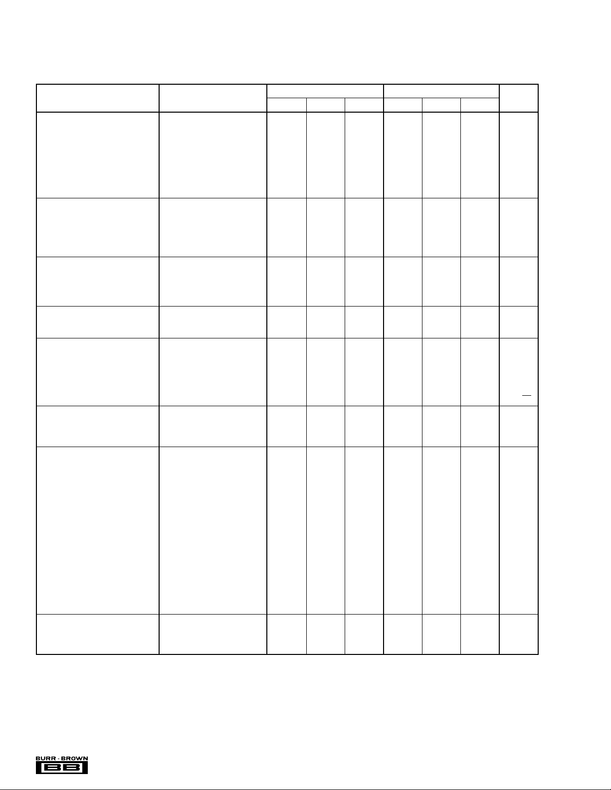
SPECIFICATIONS
ELECTRICAL
At TA = +25°C and V
PARAMETER CONDITIONS MIN TYP MAX MIN TYP MAX UNITS
ISOLATION
Rated Continuous Voltage
AC, 60Hz T
DC T
Test Breakdown, 100% AC, 60Hz 10s 5657 ✻ Vpk
Isolation-Mode Rejection 1500Vrms, 60Hz 130 ✻ dB
Barrier Impedance 10
Leakage Current 240Vrms, 60Hz 1 2 ✻✻µA
GAIN
Nominal 1 ✻ V/V
Initial Error ±0.3 ±0.5 ✻✻%FSR
Gain vs Temperature ±60 ±100 ±20 ±50 ppm/°C
Nonlinearity V
INPUT OFFSET VOLTAGE
Initial Offset ±20 ±60 ✻✻mV
vs Temperature ±300 ±500 ±100 ±250 µV/°C
vs Power Supplies V
vs Output Supply Load I
SIGNAL INPUT
Voltage Range Output Voltage in Range ±10 ±15 ✻✻ V
Resistance 200 ✻ kΩ
SIGNAL OUTPUT
Voltage Range ±10 ±12.5 ✻✻ V
Current Drive ±5 ±15 ✻✻ mA
Ripple Voltage, 800kHz Carrier 25 ✻ mVp-p
Capacitive Load Drive 1000 ✻ pF
Voltage Noise 4 ✻ µV/√Hz
FREQUENCY RESPONSE
Small Signal Bandwidth 20 ✻ kHz
Slew Rate 1.5 ✻ V/µs
Settling Time 0.1%, –10/10V 75 ✻ µs
POWER SUPPLIES
Rated Voltage, V
Voltage Range ±10 ±18 ✻✻V
Input Current I
Ripple Current No Filter 60 ✻ mAp-p
Rated Output Voltage Load = 15mA ±14.25 ±15 ±15.75 ✻✻✻ V
Output 50mA Balanced Load 10 ✻ V
Load Regulation Balanced Load 0.3 ✻ %/mA
Line Regulation 1.12 ✻ V/V
Output Voltage vs Temperature 2.5 ✻ mV/°C
Voltage Balance, ±V
Voltage Ripple (800kHz) No External Capacitors 50 ✻ mVp-p
Output Capacitive Load 1 ✻ µF
Sync Frequency Sync-Pin Grounded
TEMPERATURE RANGE
Specification –25 +85 ✻✻°C
Operating –25 +85 ✻✻°C
Storage –25 +125 ✻✻°C
✻ Specifications same as ISO113.
NOTE: (1) Conforms to UL1244 test methods. 100% tested at 1500Vrms for 1 minute. (2) If using external synchronization with a TTL-level clock, frequency should
be between 1.2MHz and 2MHz with a duty-cycle greater than 25%.
= ±15V, ±15mA output, current unless otherwise noted.
CC1
to T
MIN
MAX
to T
MIN
MAX
2121VDC 160 ✻ dB
= –10V to 10V ±0.05 ±0.1 ±0.03 ±0.05 %FSR
O
V
= –5V to 5V ±0.02 ±0.04 ±0.012 ±0.02 %FSR
O
= ±10 to ±18V 0.9 ✻ mV/V
CC2
= 0 to ±50mA ±0.3 ✻ mV/mA
O
400Ω/4.7nF (See Figure 4) 5 ✻ mVp-p
CC1
= ±15mA +90/–4.5 ✻ mA
O
I
= 0mA +60/–4.5 ✻ mA
O
C
= 1µF3 ✻ mAp-p
IN
100mA Single-Ended Load 10 ✻ V
CC2
C
= 1µF5 ✻ mVp-p
EXT
(2)
ISO113 ISO113B
1500 ✻ Vrms
2121 ✻ VDC
12
|| 9 ✻ Ω || pF
±15 ✻ V
0.05 ✻ %
1.6 ✻ MHz
®
ISO113
2
Page 3
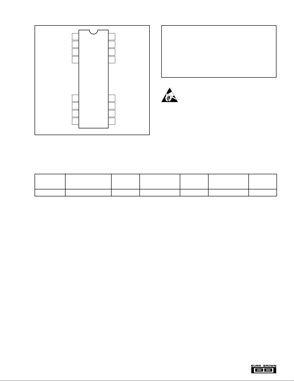
PIN CONFIGURATION ABSOLUTE MAXIMUM RATINGS
Supply Without Damage ....................................................................±18V
V
, Sense Voltage............................................................................. ±50V
Enable
+V
CC1
Sync
–V
CC1
1
2
3
4
24
NC
23
Gnd 1
22
V
IN
21
Com 1
IN
Com
to Gnd
1
Enable, Sync......................................................................... Gnd to +V
Continuous Isolation Voltage .....................................................1500Vrms
V
, dv/dt ..................................................................................... 20kV/µs
ISO
Junction Temperature .................................................................... +150°C
Storage Temperature...................................................... –25°C to +125°C
Lead Temperature,10s .................................................................. +300°C
Output Short to Gnd Duration .................................................. Continuous
±V
CC2
................................................................................................................±200mV
1
to Gnd 2 Duration .......................................................... Continuous
ELECTROSTATIC
Gnd 2
V
OUT
Sense
Ps Gnd
9
10
11
12
16
–V
C
15
–V
CC2
14
+V
CC2
13
+V
C
This integrated circuit can be damaged by ESD. Burr-Brown
recommends that all integrated circuits be handled with
appropriate precautions. Failure to observe proper handling
DISCHARGE SENSITIVITY
and installation procedures can cause damage.
ESD damage can range from subtle performance degradation
to complete device failure. Precision integrated circuits may
be more susceptible to damage because very small parametric
changes could cause the device not to meet its published
specifications.
CC1
PACKAGE/ORDERING INFORMATION
PACKAGE SPECIFIED
DRAWING TEMPERATURE PACKAGE ORDERING TRANSPORT
PRODUCT PACKAGE NUMBER
ISO113 24-Pin DIP 231 –25°C to +85°C
NOTES: (1) For detailed drawing and dimension table, please see end of data sheet, or Appendix C of Burr-Brown IC Data Book. (2) Models with a slash (/ ) are
available only in Tape and Reel in the quantities indicated (e.g., /2K5 indicates 2500 devices per reel). Ordering 2500 pieces of “ISO113/2K5” will get a single 2500piece Tape and Reel. For detailed Tape and Reel mechanical information, refer to Appendix B of Burr-Brown IC Data Book.
(1)
RANGE MARKING NUMBER
(2)
MEDIA
The information provided herein is believed to be reliable; however, BURR-BROWN assumes no responsibility for inaccuracies or omissions. BURR-BROWN assumes
no responsibility for the use of this information, and all use of such information shall be entirely at the user’s own risk. Prices and specifications are subject to change
without notice. No patent rights or licenses to any of the circuits described herein are implied or granted to any third party. BURR-BROWN does not authorize or warrant
any BURR-BROWN product for use in life support devices and/or systems.
3
ISO113
®
Page 4
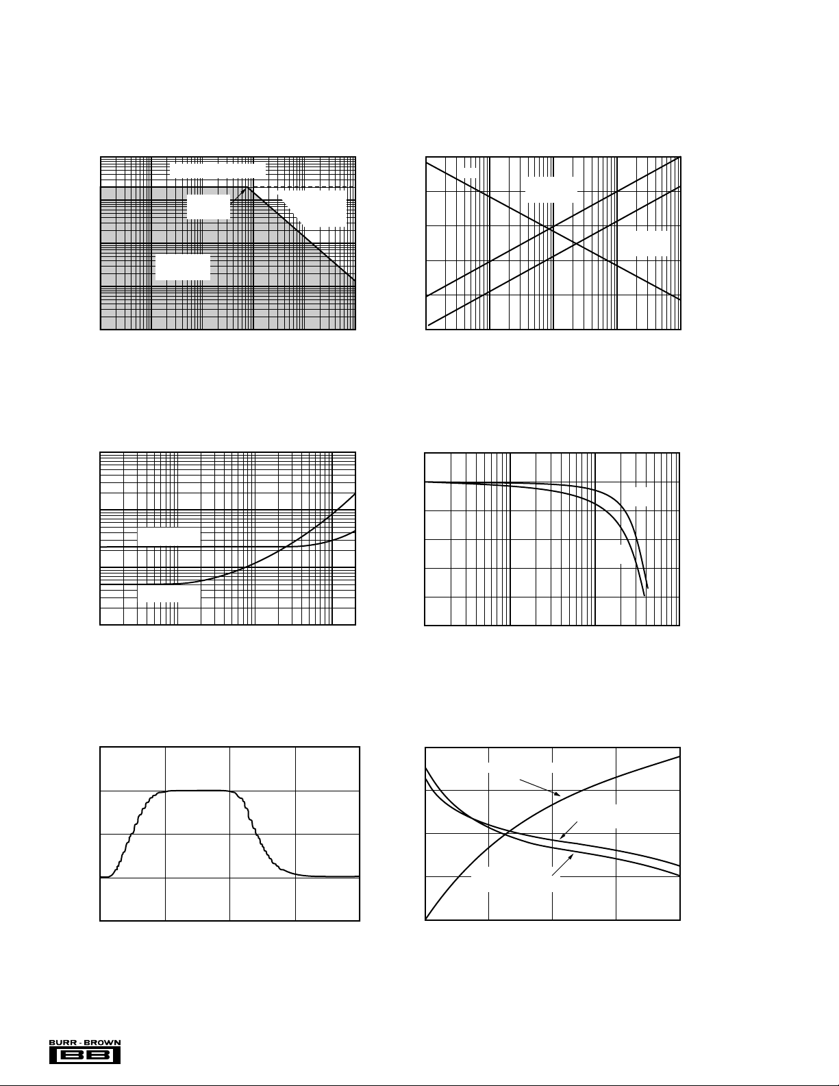
TYPICAL PERFORMANCE CURVES
At TA = +25°C,V
= ±15VDC, ±15mA output, current unless otherwise noted.
CC1
RECOMMENDED RANGE OF ISOLATION VOLTAGE
10k
2.1k
1k
100
10
Maximum Isolation Voltage (Vpk)
1
100 1k 10k 100k 1M 10M
10
1
THD + N (%)
0.1
Barrier Voltage Rating
2100V
at 75kHz
Operational
Region
Isolation Voltage Frequency (Hz)
DISTORTION vs FREQUENCY
V = 2Vp-p
O
Non-Specified
Signal
Operation
140
130
120
110
100
Isolation-Mode Rejection (dB)
90
10 100 1k 10k 100k
3
0
–3
–6
Gain (dB)
–9
IMR/LEAKAGE vs FREQUENCY
IMR
Isolation Voltage Frequency (Hz)
GAIN/PHASE vs FREQUENCY
Leakage at
1500Vrms
Leakage at
240Vrms
Phase
Gain
10mA
1mA
100µA
10µA
1µA
100nA
0
45
90
135
Barrier Leakage Current (rms)
Phase Shift (°)
V = 20Vp-p
O
0.01
10
20
10
0
Output Voltage (V)
–10
–20
0 50 100
100 10k
Frequency (Hz)
LARGE SIGNAL TRANSIENT RESPONSE
1k
Time (µs)
–12
–15
ISOLATED POWER SUPPLY
17
16
15
CC1
14
±V Output Voltage (V)
13
0
0
LOAD REGULATION AND EFFICIENCY
Balanced Load Efficiency
Output Voltage
Single-Ended Loads
10
20
±V Supply Output Current (mA)
CC1
1k100 10k 100k
Small Signal Frequency (Hz)
Output Voltage
Balanced Loads
20
40
30
60
180
60
45
30
Efficiency (%)
15
0
40
80
®
ISO113
4
Page 5
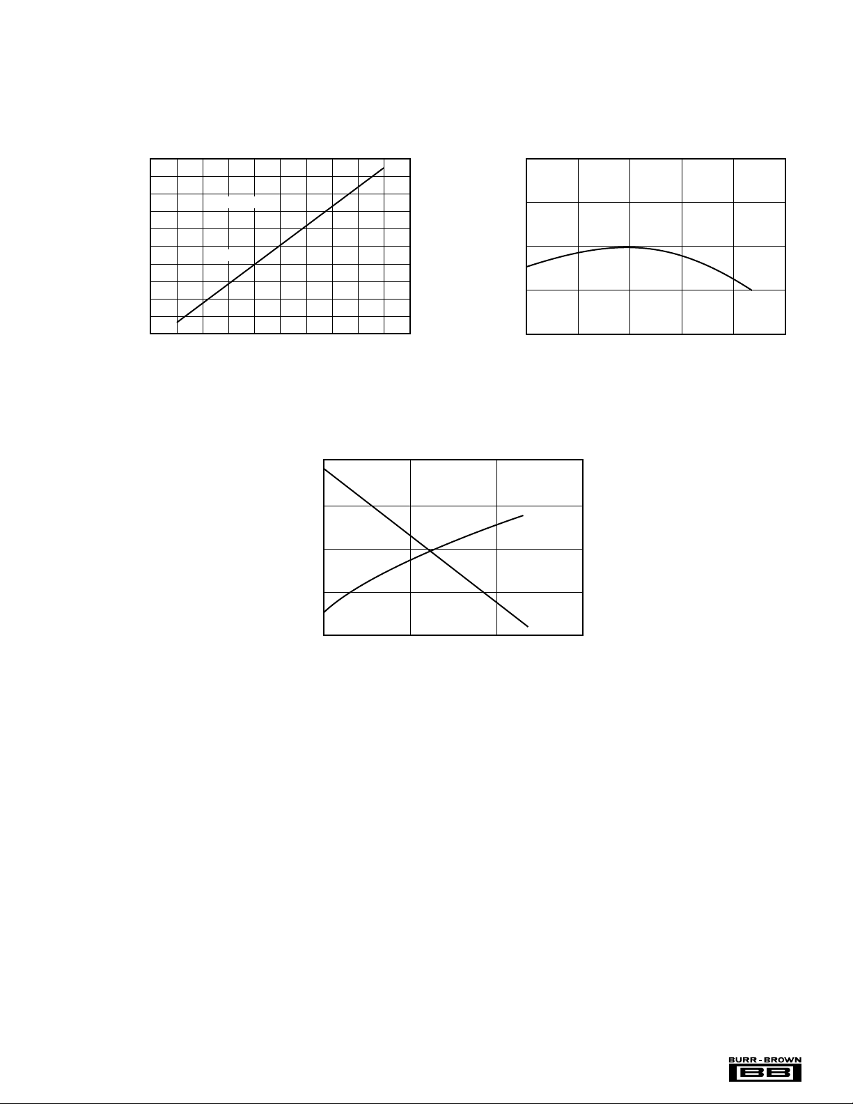
TYPICAL PERFORMANCE CURVES (CONT)
ISOLATION POWER SUPPLY VOLTAGE
vs TEMPERATURE
–25 0 25 50 75 100
Temperature (°C)
2
1
0
–1
–2
V (%)∆
CC2
At TA = +25°C,V
19
18
17
16
15
14
CC2
13
±V (V)
12
11
10
9
= ±15VDC, ±15mA output current, unless otherwise noted.
CC1
ISOLATED POWER SUPPLY LINE REGULATION
±15mA Load
1.12V/V
9 10111213141516171819
+V (V)
CC1
ISOLATED SUPPLY VOLTAGE AND V
vs SYNC FREQUENCY
5
V
CC2
2.5
0
OS
∆ V (mA)
–2.5
–5
1 1.5 2 2.5
Sync Frequency (MHz)
OS
250
125
V
OS
0
CC2
∆V (mA)
–125
–250
5
ISO113
®
Page 6
Isolation Barrier
V
IN
C
O
LO*
LO*
C
O
–
+
Supply
Outputs
23 22 21
Com 1Gnd 1
V
IN
ISO 113
(1) (2)
+V
CC1
1234
(3)
L
I
C
1µF
1µF
1
–V
SyncEnable
CC1
C
2
I
= 10µH, <10Ω.
+V
–V
24
NC
10µF
Tantalum
CC1
CC1
NOTES: (1) Enable = pin open or TTL high. (2) Ground sync if not used.
(3) π filter reduces ripple current; L
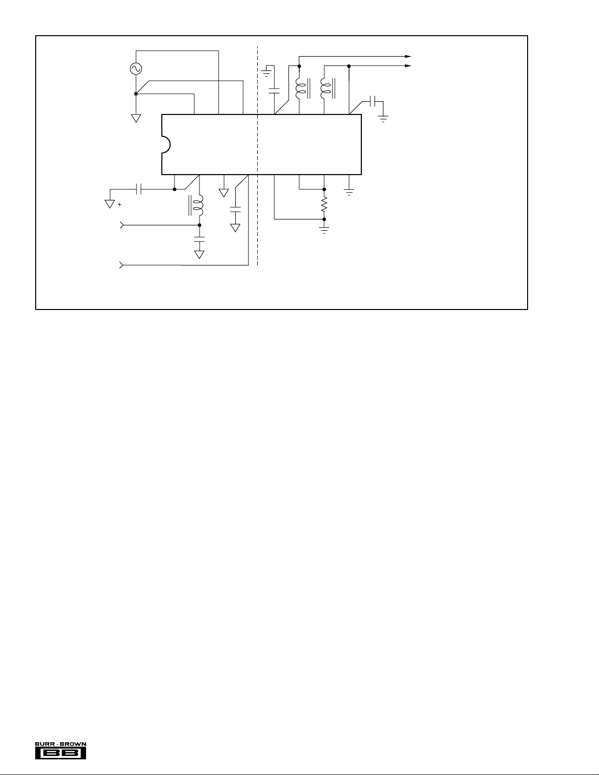
FIGURE 1. Signal and Power Connections.
THEORY OF OPERATION
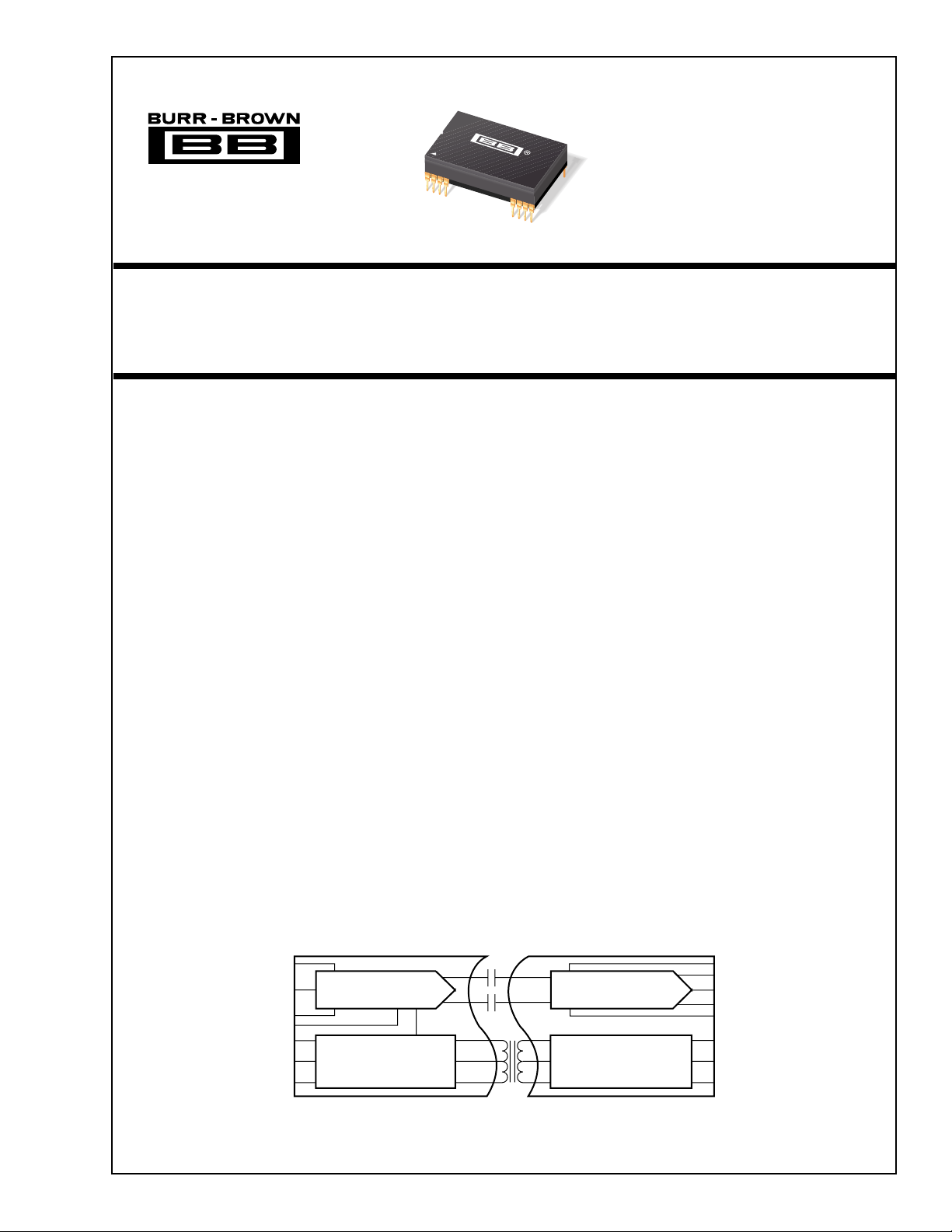
The block diagram on the front page shows the isolation
amplifier’s synchronized signal and power configuration,
which eliminate beat frequency interference. A proprietary
800kHz oscillator chip, power MOSFET transformer drivers, patented square core wirebonded transformer, and single
chip diode bridge provide power to the output side of the
isolation amplifier as well as external loads. The signal
channel capacitively couples a duty-cycle encoded signal
across the ceramic high-voltage barrier built into the package. A proprietary transmitter-receiver pair of integrated
circuits, laser trimmed at wafer level, and coupled through a
pair of matched “fringe” capacitors, results in a simple,
reliable design.
SIGNAL AND POWER CONNECTIONS
Figure 1 shows the proper power supply and signal connections. All power supply pins should be bypassed as shown
with the π filter for +V
than ±15mA are drawn from the isolated supply. Separate
rectifier output pins (±V
(±VC) allow additional ripple filtering and/or regulation. The
separate input common pin and output sense are low current
inputs tied to the signal source ground, and output load,
respectively, to minimize errors due to IR drop in long
conductors. Otherwise, connect Com 1 to Gnd 1, and Sense
to V
at the ISO113 socket. The enable pin may be left
OUT
open if the ISO113 is continuously operated. If not, a TTL
low level will disable the internal DC/ DC converter. The
Sync input must be grounded for unsynchronized operation
while a 1.2MHz to 2MHz TTL clock signal provides synchronization of multiple units.
, an option recommended if more
CC1
) and amplifier supply input pins
CC2
16 15 14 13
–V
C–VCC2+VCC2+VC
V
OUT
Gnd 2
91112
Sense
10
Ps
Gnd
R
L
The ISO113 isolation amplifier contains a transformercoupled DC/DC converter that is powered from the input
side of the isolation amplifier. All power supply pins (2, 4,
13, 14, 15, and 16) of the ISO113 have an internal 0.1µF
capacitor to ground. L1 is used to slow down fast changes in
the input current to the DC/DC converter. C1 is used to help
regulate the voltage ripple caused by the current demands of
the converter. L1, C1, and C2 are optional, however, recommended for low noise applications.
The DC/DC converter creates an unregulated ±15V output
to ±V
. If the ISO113 is the only device using the DC/DC
CC2
converter for power, pins 13 and 14 and pins 15 and 16 can
be connected directly without CO or LO in the circuit. If an
external capacitor is used in this configuration, it should not
exceed 1µF. This configuration is possible because the
isolation amplifier and the DC/DC converter are synchronized internally.
If additional devices are powered by the DC/DC converter
of the ISO113, the application may require that the ripple
voltage of the ISO113 converter be attenuated, in which
case, LO and CO should be added to the circuit. The inductor
is used to attenuate the ripple current and a higher value
capacitor can be used to reduce the ripple voltage even
further.
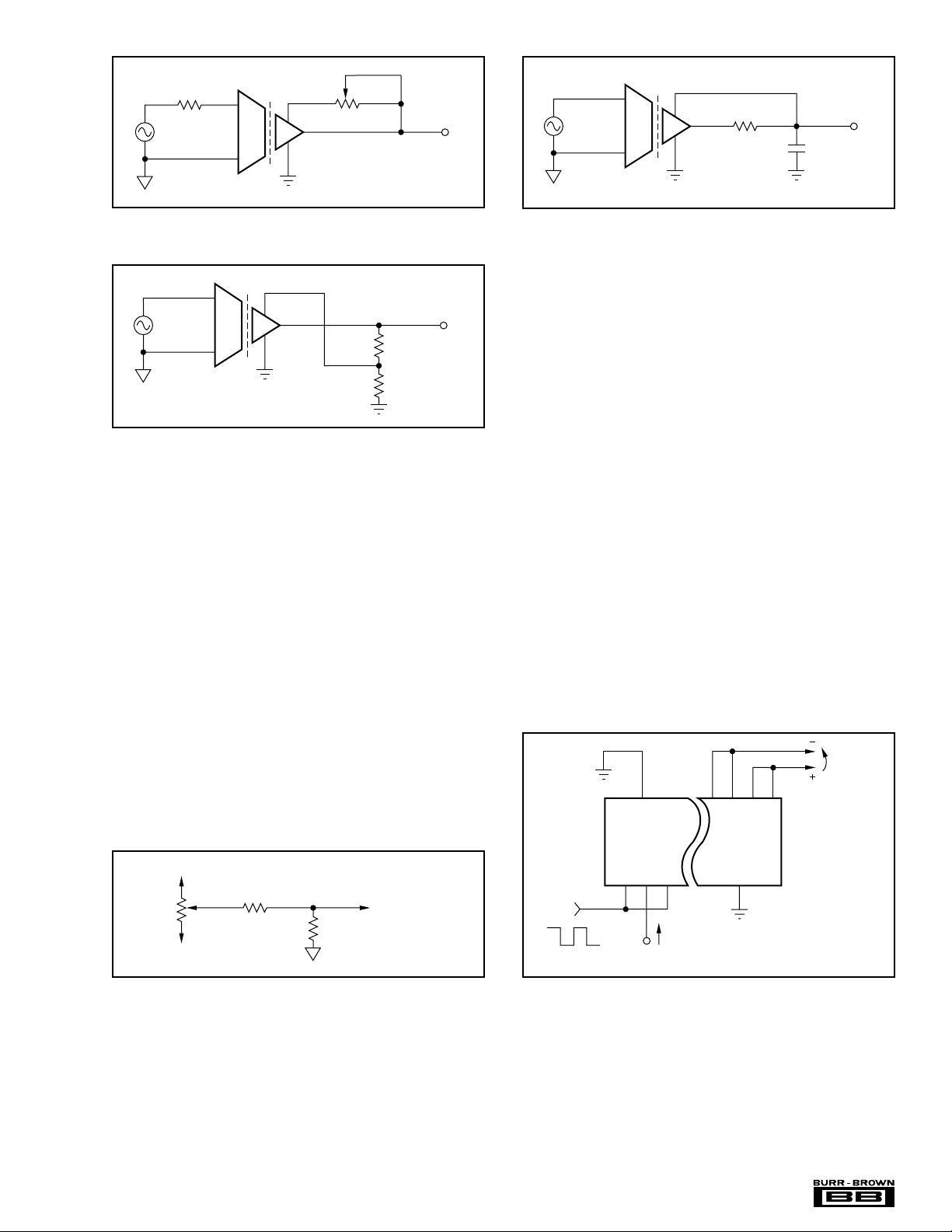
OPTIONAL GAIN AND OFFSET ADJUSTMENTS
Rated gain accuracy and offset performance can be achieved
with no external adjustments, but the circuit of Figure 2a may
be used to provide a gain trim of ±0.5% for the values shown.
Greater range may be provided by increasing the size of R1 and
R2. Every 2kΩ increase in R1 will give an additional 1%
* Optional Filtering
For L
O
0 ≤ LO < 10µH
C
< 1µF
O
For L
O
LO ≥ 10µH, <10Ω
C
≤ 10µF
O
®
ISO113
6
Page 7
Sense
4.7nF
V
OUT
11
9
400Ω
10
2kΩ
R
2
V
OUT
22
V
IN
21
R
1
22
1kΩ
V
IN
21
11
10
9
FIGURE 2a. Gain Adjust.
11
9
Sense
10
V
OUT
R
1
R
2
22
V
IN
21
Gain = 1 + (R1/R2+ R1/200k)
FIGURE 2b. Gain Setting.
adjustment range, with R2 ≥ 2R1. If safety or convenience
dictate location of the adjustment potentiometer on the other
side of the barrier from the position shown in Figure 2a, the
position of R1 and R2 may be reversed.
Gains greater than 1 may be obtained by using the circuit of
Figure 2b. Note that the effect of input referred errors will be
multiplied at the output in proportion to the increase in gain.
Also, the small-signal bandwidth will be decreased in inverse proportion to the increase in gain. In most instances, a
precision gain block at the input of the isolation amplifier
will provide better overall performance.
Figure 3 shows a method for trimming VOS of the ISO113.
This circuit may be applied to Signal Com1. With the values
shown, ±15V supplies and unity gain, the circuit will provide ±150mV adjustment range and 0.25mV resolution with
a typical trim potentiometer. The output will have some
sensitivity to power supply variations. For a ±100mV trim,
power supply sensitivity is 8mV/V at the output.
+V
or +V
CC1
CC2
100kΩ
–V
CC1
or –V
1MΩ
10kΩ
CC2
Signal Com 1
FIGURE 4. Ripple Reduction.
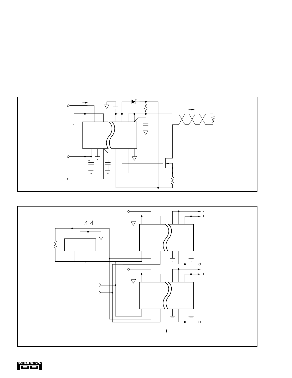
MULTICHANNEL SYNCHRONIZATION
Synchronization of multiple ISO113s can be accomplished
by connecting pin 3 of each device to an external TTL level
oscillator, as shown in Figure 7. The PWS750-1 oscillator is
convenient because its nominal synchronizing output frequency is 1.6MHz, resulting in a 800kHz carrier in the
ISO113 (its nominal unsynchronized value). The open collector output typically switches 7.5mA to a 0.2V low level
so that the external pull up resistor can be chosen for
different pull-up voltages as shown in Figure 7. The number
of channels synchronized by one PWS750-1 is determined
by the total capacitance of the sync voltage conductors. They
must be less than 1000pF to ensure TTL level switching at
800kHz. At higher frequencies the capacitance must be
proportionally lower.
Customers can supply their own TTL level synchronization
logic, provided the frequency is between 1.2MHz and 2MHz,
and the duty cycle is greater than 25%.
Single or multichannel synchronization with reduced power
dissipation for applications requiring less than ±15mA from
V
is accomplished by driving both the Sync input pin (3)
CC1
and Enable pin (1) with the TTL oscillator as shown in
Figure 5.
External
Load
<15mA
TTL Oscillation
23
ISO
123
IQ(Reduced)
+V
CC1
15141316
113
12
FIGURE 3. VOS Adjust.
OPTIONAL OUTPUT FILTER
Figure 4 shows an optional output ripple filter that reduces
the 800kHz ripple voltage to <5mVp-p without compromising DC performance. The small signal bandwidth is extended above 30kHz as a result of this compensation.
FIGURE 5. Reduced Power Dissipation.
ISOLATION BARRIER VOLTAGE
The typical performance of the ISO113 under conditions of
barrier voltage stress is indicated in the first two performance curves—Recommended Range of Isolation Voltage
and IMR/ Leakage vs Frequency. At low barrier modulation
7
ISO113
®
Page 8
levels, errors can be determined by the IMRR characteristic.
At higher barrier voltages, typical performance is obtained
as long as the dv/dt across the barrier is below the shaded
area in the first curve. Otherwise, the signal channel will be
interrupted, causing the output to distort, and/or shift DC
level. This condition is temporary, with normal operation
resuming as soon as the transient subsides. Permanent damage to the integrated circuits occurs only if transients exceed
20kV/µs. Even in this extreme case, the barrier integrity is
assured.
APPLICATIONS
HIGH VOLTAGE TESTING
The ISO113 was designed to reliably operate with 1500Vrms
continuous isolation barrier voltage. To confirm barrier
integrity, a two-step breakdown test is performed on 100%
of the units. First, an 5657V peak, 60Hz barrier potential is
applied for 10s to verify that the dielectric strength of the
insulation is above this level. Following this exposure, a
1500Vrms, 60Hz potential is applied for one minute to
conform to UL1244. Life-test results show reliable operation under continuous rated voltage and maximum operating
temperature conditions.
V
+15V
–15V
IN
0 5V
23 22 21
2341
10µF
FIGURE 6. Isolated Current Loop Driver.
Sync ≈ 1.6MHz
12 14 11
PWS750-1
R
ISO
1µF
1µF
15141316
113
6.2V
10 11 129
V
IN1
Ω
20k
1µF
23 22 21
ISO
I = 0 20mA
L
VN2222
250
Ω
0.1%
15141316
113
R ≤Ω600
L
3
7
+V
CC1
R =
Ωk
7.5
+V
CC1
–V
CC1
NOTES: (1) PWS750-1 can sync > 20 ISO113s. (2) Bypass supplies as shown in Figure 1.
FIGURE 7. Synchronized-Multichannel Isolation.
®
ISO113
23 4
V
IN2
23 22 21
ISO
113
23 4
Additional
Channels
11
10 129
V
OUT1
15141316
11
10 129
V
OUT2
8
 Loading...