

ISL9V2040D3S / ISL9V2040S3S / ISL9V2040P3
EcoSPARKTM 200mJ, 400V, N-Channel Ignition IGBT
ISL9V2040D3S / ISL9V2040S3S / ISL9 V2040P3
April 2002
General Description
The ISL9V2040D3S, ISL9V2040S3S, and ISL9V2040P3 are the
next generation ignition IGBTs that offer outstanding SCIS
capability in the space saving D-Pak (TO-252), as well as the
industry standard D²-Pa k (TO-263) and TO-220 plast ic packages.
This device is intended for use in automotive ignition circuits,
specifically as a coil driver. Internal diodes provide voltage clamping
without the need for external components.
EcoSPARK™ devices can be custom made to specific clamp
voltages. Contact your nearest Fairchild sales office for more
information.
Formerly Developmental Type 49444
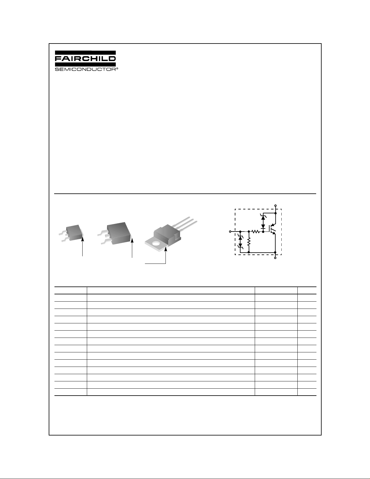
Package
JEDEC TO-252AA
D-Pak D²-Pak
G
E
COLLECTOR
(FLANGE)
JEDEC TO-263AB
G
E
COLLECTOR
(FLANGE)
Device Maximum Ratings T
JEDEC TO-220AB
= 25°C unless otherwise noted
A
Applications
• Automotive Ignition Coil Driver Circuits
• Coil- On Plug Applications
Features
• Space saving D - Pak package available
• SCIS Energy = 200mJ at T
• Logic Level Gate Drive
= 25oC
J
Symbol
E
C
G
GATE
R
1
R
2
COLLECTOR
EMITTER
Symbol Parameter Ratings Units
BV
BV
E
SCIS25
E
SCIS150
I
C25
I
C110
V
GEM
P
T
T
STG
T
T
CER
ECS
pkg
Collector to Emitter Breakdown Voltage (IC = 1 mA) 430 V
Emitter to Collector Voltage - Reverse Battery Condition (IC = 10 mA) 24 V
At Starting TJ = 25°C, I
At Starting TJ = 150°C, I
= 11.5A, L = 3.0mHy 200 mJ
SCIS
= 8.9A, L = 3.0mHy 120 mJ
SCIS
Collector Current Continuous, At TC = 25°C, See Fig 9 10 A
Collector Current Continuous, At TC = 110°C, See Fig 9 10 A
Gate to Emitter Voltage Continuous ±10 V
Power Dissipation Total TC = 25°C 130 W
D
Power Dissipation Derating T
Operating Junction Temperature Range -40 to 175 °C
J
> 25°C 0.87 W/°C
C
Storage Junction Temperature Range -40 to 175 °C
Max Lead Temp for Soldering (Leads at 1.6mm from Case for 10s) 300 °C
L
Max Lead Temp for Soldering (Package Body for 10s) 260 °C
ESD Electrostatic Discharge Voltage at 100pF, 1500Ω 4kV
©2002 Fairchild Semiconductor Corporation
ISL9V2040D3S / ISL9V2040S3S / ISL9V2040P3 Rev. B2, April 2002
Package Marking and Ordering Information
Device Marking Device Package Tape Width Quantity
V2040D ISL9V2040D3S TO-252AA 16mm 2500
V2040S ISL9V2040S3S TO-263AB 24mm 800
V2040P ISL9V2040P3 TO-220AB - -
ISL9V2040D3S / ISL9V2040S3S / ISL9 V2040P3
Electrical Characteristics
TA = 25°C unless otherwise noted
Symbol Parameter Test Conditions Min Typ Max Units
Off State Characteristics
BV
BV
BV
BV
I
CER
I
ECS
R
R
Collector to Emitter Breakdown Voltage IC = 2mA, VGE = 0,
CER
Collector to Emitter Breakdown Voltage IC = 10mA, VGE = 0,
CES
Emitter to Collector Breakdown Voltage IC = -75mA, VGE = 0V,
ECS
Gate to Emitter Breakdown Voltage I
GES
Collector to Emitter Leakage Current V
Emitter to Collector Leakage Current VEC = 24V , See
Series Gate Resistance - 70 - Ω
1
Gate to Emitter Resistance 10K - 26K Ω
2
= 1KΩ, See Fig. 15
R
G
T
= -40 to 150°C
J
= 0, See Fig. 15
R
G
= -40 to 150°C
T
J
T
= 25°C
C
= ± 2mA ±12 ±14 - V
GES
= 250V,
CER
= 1KΩ,
R
G
See Fig. 11
T
= 25°C- - 25 µA
C
= 150°C- - 1 mA
T
C
TC = 25°C- - 1 mA
Fig. 11
T
= 150°C- - 40 mA
C
370 400 430 V
390 420 450 V
30 - - V
On State Characteristics
V
CE(SAT)
V
CE(SAT)
Collector to Emitter Saturation Voltage IC = 6A,
= 4V
V
GE
Collector to Emitter Saturation Voltage IC = 10A,
= 4.5V
V
GE
T
= 25°C,
C
See Fig. 3
T
= 150°C
C
See Fig. 4
-1.451.9V
-1.952.3V
Dynamic Characteristics
Q
G(ON)
V
GE(TH)
V
GEP
Switching Characteristics
t
d(ON)R
t
riseR
t
d(OFF)L
Gate Charge IC = 10A, VCE = 12V,
Gate to Emitter Threshold Voltage IC = 1.0mA,
Gate to Emitter Plateau Voltage IC = 10A,
Current T urn-On Delay Time-Resistive V
Current Rise Time-Resistive - 2.17 - µs
Current T urn-Off Delay Time-Inductive V
Current Fall Time-Inductive - 2.36 - µs
t
fL
SCIS Self Clamped Inductive Switching T
= 5V, See Fig. 14
V
GE
= V
V
CE
GE,
See Fig. 10
= 12V
V
CE
= 14V, RL = 1Ω,
CE
V
= 5V, RG = 1KΩ
GE
= 25°C
T
J
= 300V, L = 500µHy,
CE
V
= 5V, RG = 1KΩ
GE
= 25°C, See Fig. 12
T
J
= 25°C, L = 3.0mHy,
J
= 1KΩ, VGE = 5V, See
R
G
= 25°C1.3 - 2.3 V
T
C
= 150°C0.75 - 1.8 V
T
C
Fig. 1 & 2
-12-nC
-3.4- V
-0.61- µs
-3.64- µs
- - 200 mJ
Thermal Characteristics
R
©2002 Fairchild Semiconductor Corporation ISL9V2040D3S / ISL9V2040S3S / ISL9V2040P3 Rev. B2, April 2002
Thermal Resistance Junction-Case T O-252, TO-263, TO-220 - - 1.15 °C/W
θJC
Typical Performance Curves (Continued)
ISL9V2040D3S / ISL9V2040S3S / ISL9 V2040P3
20
18
16
14
12
10
TJ = 150°C
8
6
4
, INDUCTIVE SWITCHING CURRENT (A)
2
SCIS
I
SCIS Curves valid for V
0
t
RG = 1KΩ, VGE = 5V,Vdd = 14V
TJ = 25°C
Voltages of <430V
clamp
, TIME IN CLAMP (µS)
CLP
16014012001004020 60 80
180 200
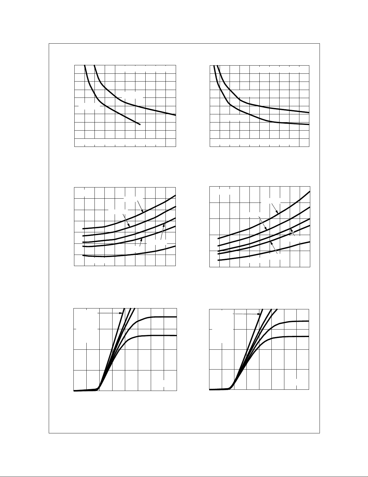
Figure 1. Self Clamped Inductive Switching
Current vs Time in Clamp
1.60
ICE = 6A
1.55
1.50
1.45
1.40
1.35
1.30
, COLLECTOR TO EMITTER VOLTAGE (V)
CE
V
1.25
-75 25-25 17512575
VGE = 8.0V
T
, JUNCTION TEMPERATURE (°C)
J
VGE = 3.7V
VGE = 4.0V
VGE = 4.5V
VGE = 5.0V
Figure 3. Collector to Emitter On-State Voltage vs
Junction Temperature
20
18
16
14
12
10
8
6
4
, INDUCTIVE SWITCHING CURRENT (A)
2
SCIS
I
0
0102468
TJ = 150°C
SCIS Curves valid for V
RG = 1KΩ, VGE = 5V,Vdd = 14V
TJ = 25°C
Voltages of <430V
clamp
L, INDUCTANCE (mHy)
Figure 2. Self Clamped Inductive Switching
Current vs Inductance
2.4
ICE = 10A
VGE = 4.0V
VGE = 8.0V
VGE = 3.7V
VGE = 4.5V
VGE = 5.0V
2.2
2.0
1.8
1.6
, COLLECTOR TO EMITTER VOLTAGE (V)
CE
V
1.4
-75 25-25 17512575
T
, JUNCTION TEMPERATURE (°C)
J
Figure 4. Collector to Emitter On-State Voltage
vs Junction Temperature
20
VGE = 8.0V
VGE = 5.0V
VGE = 4.5V
15
VGE = 4.0V
VGE = 3.7V
10
5
, COLLECTOR TO EMITTER CURRENT (A)
CE
I
0
02.01.0 3.0 4.0
VCE, COLLECTOR TO EMITTER VOLTAGE (V)
TJ = - 40°C
Figure 5. Collector to Emitter On-State Voltage vs
Collector Current
©2002 Fairchild Semiconductor Corporation ISL9V2040D3S / ISL9V2040S3S / ISL9V2040P3 Rev. B2, April 2002
20
VGE = 8.0V
VGE = 5.0V
VGE = 4.5V
15
VGE = 4.0V
VGE = 3.7V
10
5
, COLLECTOR TO EMITTER CURRENT (A)
CE
I
0
02.01.0 3.0 4.0
VCE, COLLECTOR TO EMITTER VOLTAGE (V)
TJ = 25°C
Figure 6. Collector to Emitter On-State Voltage
vs Collector Current

Typical Performance Curves (Continued)
ISL9V2040D3S / ISL9V2040S3S / ISL9 V2040P3
20
VGE = 8.0V
VGE = 5.0V
VGE = 4.5V
15
VGE = 4.0V
VGE = 3.7V
10
5
, COLLECTOR TO EMITTER CURRENT (A)
CE
I
0
02.01.0 3.0 4.0
VCE, COLLECTOR TO EMITTER VOLTAGE (V)
TJ = 175°C
Figure 7. Collector to Emitter On-State Voltage vs
Collector Current
15.0
VGE = 4.0V
12.5
10.0
7.5
30
DUTY CYCLE < 0.5%, VCE = 5V
PULSE DURATION = 250µs
25
20
15
10
5
, COLLECTOR TO EMITTER CURRENT (A)
CE
I
0
TJ = 150°C
TJ = 25°C
2.01.0 3.0 4.0
VGE, GATE TO EMITTER VOLTAGE (V)
Figure 8. Transfer Characteristics
2.4
2.2
2.0
1.8
TJ = -40°C
5.0
VCE = VGE
ICE = 1mA
5.0
, DC COLLECTOR CURRENT (A)
2.5
CE
I
0
25 1751257550 100 150
TC, CASE TEMPERATURE (°C)
Figure 9. DC Collector Current vs Case
Temperature
10000
V
= 24V
1000
100
10
LEAKAGE CURRENT (µA)
1
0.1
TJ, JUNCTION TEMPERATURE (°C)
ECS
V
= 300V
CES
V
= 250V
CES
25-25 17512575-50 0 50 100 150
Figure 11. Leakage Current vs Junction
Temperature
1.6
, THRESHOLD VOLTAGE (V)
TH
V
1.4
1.2
-50 1257525-25
0 50 100 150
TJ JUNCTION TEMPERATURE (°C)
Figure 10. Threshold Voltage vs Junction
Temperature
10
ICE = 6.5A, VGE = 5V, RG = 1KΩ
Inductive t
8
6
SWITCHING TIME (µS)
4
2
25 1751257550 100 150
OFF
Resistive t
OFF
T
, JUNCTION TEMPERATURE (°C)
J
Resistive t
Figure 12. Switching Time vs Junction
Temperature
175
ON
©2002 Fairchild Semiconductor Corporation ISL9V2040D3S / ISL9V2040S3S / ISL9V2040P3 Rev. B2, April 2002

Typical Performance Curves (Continued)
ISL9V2040D3S / ISL9V2040S3S / ISL9 V2040P3
1200
1000
800
600
400
C, CAPACITANCE (pF)
200
0
0105152025
C
RES
C
VCE, COLLECTOR TO EMITTER VOLTAGE (V)
C
OES
IES
FREQUENCY = 1 MHz
Figure 13. Capacitance vs Collector to Emitter
8
I
= 1mA, RL = 1.25Ω, TJ = 25°C
G(REF)
7
6
V
= 12V
CE
5
4
3
2
, GATE TO EMITTER VOLTAGE (V)
1
GE
V
0
0 5 10 15 20 25
VCE = 6V
QG, GATE CHARGE (nC)
Figure 14. Gate Charge
Voltage
415
410
405
400
395
390
385
, BREAKDOWN VOLTAGE (V)
380
CER
BV
375
370
10 20001000 3000
TJ = 175°C
TJ = 25°C
100
RG, SERIES GATE RESISTANCE (kΩ)
Figure 15. Breakdown Voltage vs Series Gate Resistance
I
= 10mA
CER
TJ = - 40°C
0
10
0.5
0.2
t
1
P
D
t
2
2
X R
θ
JC
-1
10
) + T
θ
JC
C
0
10
10
, NORMALIZED THERMAL RESPONSE
thJC
Z
10
0.1
-1
0.05
0.02
0.01
-2
-5
10
SINGLE PULSE
-4
10
-3
10
T1, RECTANGULAR PULSE DURATION (s)
10
DUTY FACTOR, D = t1 / t
PEAK TJ = (PD X Z
-2
Figure 16. IGBT Normalized Transient Thermal Impedance, Junction to Case
©2002 Fairchild Semiconductor Corporation ISL9V2040D3S / ISL9V2040S3S / ISL9V2040P3 Rev. B2, April 2002

Test Circuit and Waveforms
ISL9V2040D3S / ISL9V2040S3S / ISL9 V2040P3
L
C
R
PULSE
GEN
G
DUT
G
E
Figure 17. Inductive Switching Test Circuit
V
CE
L
VARY t
TO OBTAIN
P
REQUIRED PEAK I
V
GE
t
0V
P
AS
R
G
DUT
I
AS
0.01Ω
V
CE
R
or
LOAD
L
C
5V
RG = 1KΩ
G
DUT
+
V
CE
-
E
Figure 18. t
+
V
DD
-
0
ON
and t
I
AS
Switching Test Circuit
OFF
BV
CES
t
P
t
AV
V
CE
V
DD
Figure 19. Unclamped Energy Test Circuit Figure 20. Unclamped Energy Waveforms
©2002 Fairchild Semiconductor Corporation ISL9V2040D3S / ISL9V2040S3S / ISL9V2040P3 Rev. B2, April 2002

ISL9V2040D3S / ISL9V2040S3S / ISL9 V2040P3
SPICE Thermal Model
REV 25 April 2002
ISL9V2040D3S, I SL9V2040S3S, ISL9V2040P3
CTHERM1 th 6 1.3e -2
CTHERM2 6 5 8.8e -4
CTHERM3 5 4 8.8e -3
CTHERM4 4 3 3.9e -1
CTHERM5 3 2 3.6e -1
CTHERM6 2 tl 1.9e -1
RTHERM1 th 6 1.2e -1
RTHERM2 6 5 3.2e -1
RTHERM3 5 4 1.7e -1
RTHERM4 4 3 1.2e -1
RTHERM5 3 2 1.3e -1
RTHERM6 2 tl 2.5e -1
SABER Thermal Model
SABER thermal model
ISL9V2040D3S, I SL9V2040S3S, ISL9V2040P3
template thermal_model th tl
thermal_c th, tl
{
ctherm.ctherm1 th 6 = 1.3e -3
ctherm.ctherm2 6 5 = 8.8e -4
ctherm.ctherm3 5 4 = 8.8e -3
ctherm.ctherm4 4 3 = 3.9e -1
ctherm.ctherm5 3 2 = 3.6e -1
ctherm.ctherm6 2 t l = 1.9e -1
rtherm.rtherm1 th 6 = 1.2e -1
rtherm.rtherm2 6 5 = 3.2e -1
rtherm.rtherm3 5 4 = 1.7e -1
rtherm.rtherm4 4 3 = 1.2e -1
rtherm.rtherm5 3 2 = 1.3e -1
rtherm.rtherm6 2 tl = 2.5e -1
}
RTHERM1
RTHERM2
RTHERM3
RTHERM4
RTHERM5
JUNCTION
th
CTHERM1
6
CTHERM2
5
CTHERM3
4
CTHERM4
3
CTHERM5
2
RTHERM6
tl
©2002 Fairchild Semiconductor Corporation ISL9V2040D3S / ISL9V2040S3S / ISL9V2040P3 Rev. B2, April 2002
CTHERM6
CASE

TRADEMARKS
The following are registered and unregistered trademarks Fairchild Semiconductor owns or is authorized to use and is
not intended to be an exhaustive list of all such trademarks.
ACEx
Bottomless
CoolFET
CROSSVOL T
DenseTrench
DOME
EcoSPARK
E2CMOS
EnSigna
TM
TM
FACT
FACT Quiet Series
STAR*POWER is used under license
FAST
FASTr
FRFET
GlobalOptoisolator
GTO
HiSeC
2
I
C
ISOPLANAR
LittleFET
MicroFET
MicroPak
MICROWIRE
OPTOLOGIC
â
OPTOPLANAR
PACMAN
POP
Power247
PowerTrench
â
QFET
QS
QT Optoelectronics
Quiet Series
SILENT SWITCHER
SMART START
SPM
STAR*POWER
Stealth
SuperSOT-3
SuperSOT-6
SuperSOT-8
SyncFET
TinyLogic
TruTranslation
ââ
UHC
UltraFET
VCX
DISCLAIMER
FAIRCHILD SEMICONDUCTOR RESERVES THE RIGHT TO MAKE CHANGES WITHOUT FURTHER
NOTICE TO ANY PRODUCTS HEREIN TO IMPROVE RELIABILITY, FUNCTION OR DESIGN. FAIRCHILD
DOES NOT ASSUME ANY LIABILITY ARISING OUT OF THE APPLICATION OR USE OF ANY PRODUCT
OR CIRCUIT DESCRIBED HEREIN; NEITHER DOES IT CONVEY ANY LICENSE UNDER ITS PATENT
RIGHTS, NOR THE RIGHTS OF OTHERS.
LIFE SUPPORT POLICY
â
FAIRCHILDS PRODUCTS ARE NOT AUTHORIZED FOR USE AS CRITICAL COMPONENTS IN LIFE SUPPORT
DEVICES OR SYSTEMS WITHOUT THE EXPRESS WRITTEN APPROVAL OF FAIRCHILD SEMICONDUCTOR CORPORATION.
As used herein:
1. Life support devices or systems are devices or
systems which, (a) are intended for surgical implant into
the body, or (b) support or sustain life, or (c) whose
failure to perform when properly used in accordance
with instructions for use provided in the labeling, can be
reasonably expected to result in significant injury to the
user.
PRODUCT STATUS DEFINITIONS
Definition of Terms
Datasheet Identification Product Status Definition
Advance Information
Preliminary
No Identification Needed
Formative or
In Design
First Production
Full Production
2. A critical component is any component of a life
support device or system whose failure to perform can
be reasonably expected to cause the failure of the life
support device or system, or to affect its safety or
effectiveness.
This datasheet contains the design specifications for
product development. Specifications may change in
any manner without notice.
This datasheet contains preliminary data, and
supplementary data will be published at a later date.
Fairchild Semiconductor reserves the right to make
changes at any time without notice in order to improve
design.
This datasheet contains final specifications. Fairchild
Semiconductor reserves the right to make changes at
any time without notice in order to improve design.
Obsolete
Not In Production
This datasheet contains specifications on a product
that has been discontinued by Fairchild semiconductor.
The datasheet is printed for reference information only.
Rev. H5
 Loading...