

Page 1
®
ISL97635A
Data Sheet December 22, 2008
SMBus 6-Channel LED Driver
The ISL97635A is a digitally control led LED driver that
controls 6 channels of LED current for LCD backlight
applications. The ISL97635A is capable of driving typically
54 (6x9) pieces of 3.5V/30mA or 60 (6x10) pieces of
3.2V/20mA LEDs. The ISL97635A contains 6 channels of
voltage controlled current sources with typical currents
matching of ±1%, which compensate for the non-uniformity
effect of forward voltages variance in the LED stacks. To
minimize the voltage headroom and power loss in the typical
multi-strings operation, the ISL97635A features a dynamic
headroom control that monitors the highest LED forward
voltage string and uses its feedback signal for output
regulation.
The LED dimming control can be achieved through a
SMBus, an external PWM, or a variable DC (analog light
sensor) input. SMBus controlled dimming allows 256 levels
each of PWM and DC current adjustments. The SMBus
PWM dimming frequency can be adjusted from 100Hz to
5kHz by an external capacitor. External PWM input allows up
to 20kHz audio noise free PWM dimming. The SMBus PWM
setting and an external PWMI signal can also be combined
to provide a dynamic PWM dimming that complies with
Intel’s DPST (Display Power Saving Technology)
requirement.
One or more channels can be selected sequentially in any
order allowing scrolling in RGB LED backlighting
applications.
The ISL97635A features ex te ns ive protection functions that
include string open and short circuit detections, OVP, OTP,
thermal shutdown and an optional input overcurrent
protection with master fault disconnect switch. The fault
conditions will be recorded in the Fault/Status register. There
are selectable short-circuit thresholds and the switching
frequency can be programmed between 600kHz and
1.2MHz.
Available in the 24 Ld 4mmx4mm QFN, the ISL97635A
operates from -40°C to +85°C with input voltage ranging
from 6V to 24V for high LEDs count applications.
FN6564.2
Features
• 6 Channels
• 6V to 24V Input
• 34.5V Output Max
• Drive Maximally 54 (3.5V/30mA each) or 60 (3.2V/20mA
each) LEDs
• Current Matching ±1% Typ
• Dynamic Headroom Control
• Dimming Controls
- SMBus 8-Bit PWM Current Control
- SMbus 8-Bit DC Current Control
- External PWM Input up to 20kHz Dimming
- SMBus and External PWM DPST Dimming Control
- DC-to-PWM Dimming Control
• Protections
- String Open Circuit Detection
- String Short Circuit Detection with Selectable
Thresholds
- Over-Temperature Protection
- Overvoltage Protection
- Input Overcurrent Protection with Disconnect Switch
• 600kHz/1.2MHz Selectable f
SW
• Selectable Channels Allows Scrolling Backlight
• 24 Ld (4mmx4mm) QFN Package
• Pb-Free (RoHS Compliant)
Applications
• Notebook Displays WLED or RGB LED Backlighting
• LCD Monitor LED Backlighting
• Automotive Displays LED Backlighting
• Automotive or Traffic Lighting
Ordering Information
PART
NUMBER
(Note)
ISL97635AIRZ* 976 35AIRZ 24 Ld 4x4 QFN L24.4x4D
*Add “-T” or “-TK” suffix for tape and reel. Please refer to TB347 for
details on reel specifications
NOTE: These Intersil Pb-free plastic packaged products employ
special Pb-free material sets, molding compounds/die attach
materials, and 100% matte tin plate plus anneal (e3 termination
finish, which is RoHS compliant and compatible with both SnPb and
Pb-free soldering operations). Intersil Pb-free products are MSL
classified at Pb-free peak reflow temperatures that meet or exceed
the Pb-free requirements of IPC/JEDEC J STD-020.
PART
MARKING
PACKAGE
(Pb-Free)
PKG.
DWG. #
1
CAUTION: These devices are sensitive to electrostatic discharge; follow proper IC Handling Procedures.
1-888-INTERSIL or 1-888-468-3774
| Intersil (and design) is a registered trademark of Intersil Americas Inc.
All other trademarks mentioned are the property of their respective owners.
Copyright Intersil Americas Inc. 2008. All Rights Reserved
Page 2
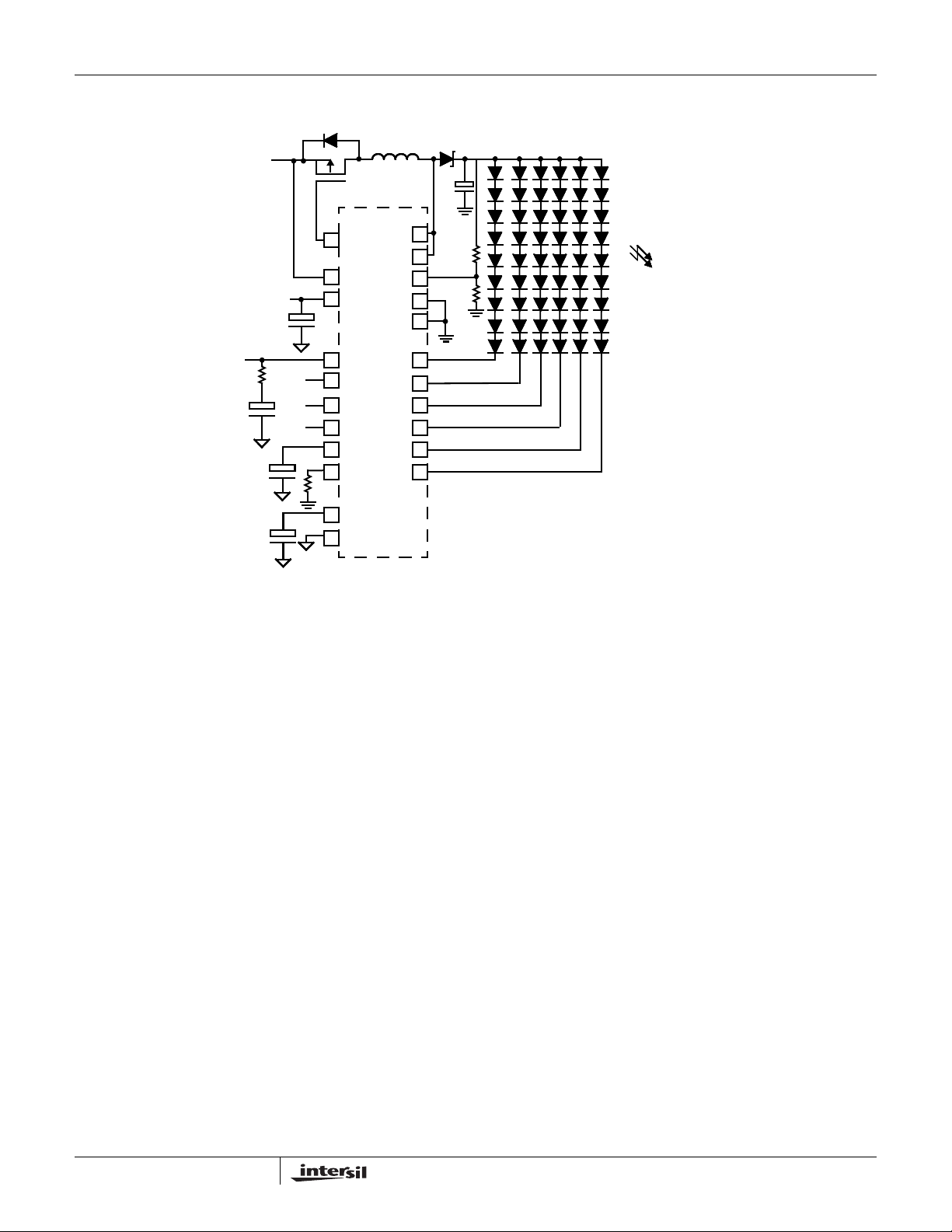
Typical Application Circuit
VBL+ = 6V TO 24V
21
23
24
ISL97635A
FAULT
VIN
VDC
LX
LX
OVP
PGND
PGND 18
ISL97635A
= 34.5V, 30mA PER STRING
V
OUT
19
20
16
17
22
1
2
6
4
11
3
5
COMP
SMBCLK
SMBDAT
PWMI/EN
PWMO
RSET
FPWM
GND
IIN0
IIN1
IIN2
IIN3
IIN4
IIN5
15
14
13
12
10
9
2
FN6564.2
December 22, 2008
Page 3
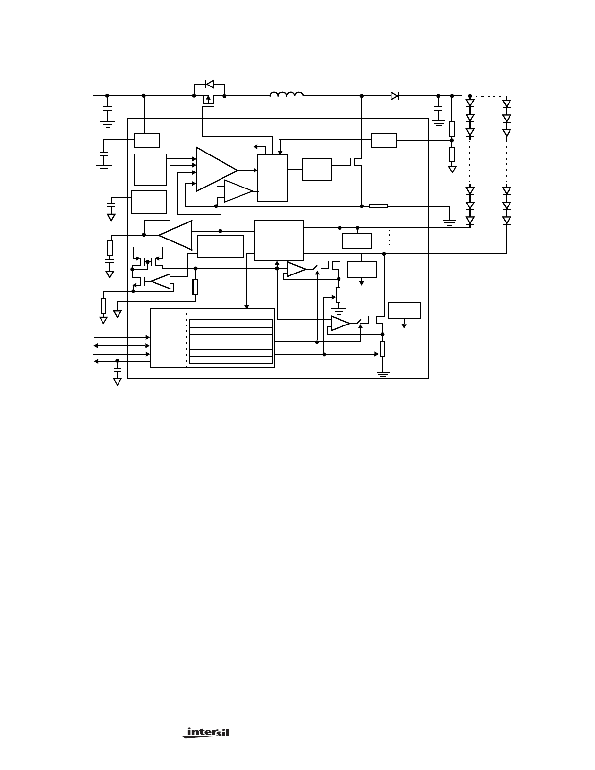
Block Diagram
VBL+ = 6V TO 24V
ISL97635A
34.5V, 30mA PER STRING
(6 x 9 = 54 WHITE LEDS)
SMBCLK
SMBDAT
PWMI
PWMO
VDC
f
PWM
COMP
RSET
GND
VIN
VIN
REG
OSC AND
RAMP
COMP
LED PWM
CONTROL
INTERFACE
INTERFACE
+
+
-
-
SMBUS
FAULT
FAULT/STATUS
REGISTER
Σ = 0
ILIMIT
IMAX
GM
AMP
REFERENCE
GENERAT OR
REGISTERS
PWM BRIGHTNESS CONTROL
DEVICE CONTROL
FAULT/STATUS
IDENTIFICATION
DC BRIGHTNESS CONTROL
CONFIGURATION
LOGIC
HIGHEST VF
STRING
DETECT
+
+
-
-
PWM/OC/SC
AM
ISL97635A
FET
DRIVER
OC, SC
DETECT
OC, SC
DETECT
FAULT/STATUS
REGISTER
+
+
-
-
LX
LX
OVP
IIN0
IIN5
TEMP
SENSOR
FAUL T/STATUS
REGISTER
PGND
FIGURE 1. ISL97635A BLOCK DIAGRAM
3
FN6564.2
December 22, 2008
Page 4
ISL97635A
Absolute Maximum Ratings (T
VIN, FAULT . . . . . . . . . . . . . . . . . . . . . . . . . . . . . . . . . .-0.3V to 24V
VDC, COMP, RSET . . . . . . . . . . . . . . . . . . . . . . . . . . . -0.3V to 6.5V
SMBCLK, SMBDAT, FPWM, PWMO, EN/PWM . . . . . -0.3V to 6.5V
OVP, IIN0 - IIN5 . . . . . . . . . . . . . . . . . . . . . . . . . . . . . . .-0.3V to 28V
LX. . . . . . . . . . . . . . . . . . . . . . . . . . . . . . . . . . . . . . . . . .-0.3V to 36V
PGND. . . . . . . . . . . . . . . . . . . . . . . . . . . . . . . . . . . . . -0.3V to +0.3V
Above voltage ratings are all with respect to GND pin
= +25°C) Thermal Information
A
Thermal Resistance (Typical, Notes 1, 2) θ
24 Ld QFN . . . . . . . . . . . . . . . . . . . . . . 39 2
Thermal Characterization (Typical, Note 3) PSI
24 Ld QFN . . . . . . . . . . . . . . . . . . . . . . . . . . . . . . . . ~0.7
Maximum Continuous Junction Temperature . . . . . . . . . . . .+125°C
Storage Temperature . . . . . . . . . . . . . . . . . . . . . . .-65°C to +150°C
Pb-free Reflow Profile . . . . . . . . . . . . . . . . . . . . . . . . .see link below
(°C/W) θJC (°C/W)
JA
(°C/W)
JT
http://www.intersil.com/pbfree/Pb-FreeReflow.asp
Operating Conditions
Temperature Range . . . . . . . . . . . . . . . . . . . . . . . . . .-40°C to +85°C
IMPORTANT NOTE: All parameters having Min/Max specifications are guaranteed. Typical values are for information purposes only. Unless otherwise noted, all tests
are at the specified temperature and are pulsed tests, therefore: T
CAUTION: Do not operate at or near the maximum ratings listed for extended periods of time. Exposure to such conditions may adversely impact product reliability and
result in failures not covered by warranty.
NOTES:
is measured in free air with the component mounted on a high effective thermal conductivity test board with “direct attach” features. See T ech
1. θ
JA
Brief TB379.
2. For θ
3. PSI
, the “case temp” location is the center of the exposed metal pad on the package underside assumed under ideal case temperature.
JC
is the junction-to-top thermal resistance. If the package top temperature can be measured, with this rating then the die junction temperature
JT
can be estimated more accurately than the θ
JC
4. Limits established by characterization and are not production tested.
Electrical Specifications All specifications below are tested at T
otherwise noted. Parameters with MIN and/or MAX limits are 100% tested at +25°C, unless otherwise
specified. Temperature limits established by characterization and are not production tested.
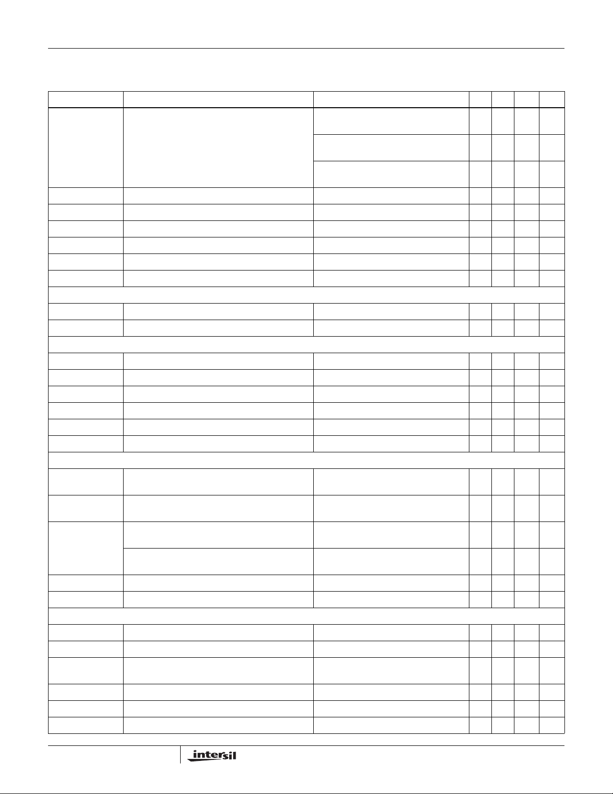
PARAMETER DESCRIPTION CONDITION MIN TYP MAX UNIT
GENERAL
VIN Backlight Supply Voltage ≤ 9 LEDs per channel (3.5V/30mA type) 6 24 V
IVIN_STBY VIN Shutdown Current 5µA
V
OUT
V
UVLO
V
UVLO_HYS
REGULATOR
V
DC
I
VDC_STBY
I
VDC
V
LDO
SS Soft-Start 1ms
ENmin Minimum Enable Signal 40 µs
BOOST
SWILimit Boost FET Current Limit T
r
DS(ON)
Output Voltage 34.5 V
Undervoltage Lockout Threshold 2.45 2.8 V
Undervoltage Lockout Hysteresis 300 mV
LDO Output Voltage VIN >6V 5.0 5.5 V
Standby Current EN/PWM = 0V 20 µA
Active Current EN/PWM = 5V 10 mA
VDC LDO Dropout Voltage VIN > 5.5V, 30mA 30 200 mV
Internal Boost Switch ON-Resistance 130 260 mΩ
= TC = T
J
A
and θJC thermal resistance ratings.
= -40°C to +85°C; VIN = 12V, EN = 5V, R
A
= +25°C 2.3 3.2 A
A
= -40°C to +85°C 2.2 A
T
A
= 36.6kΩ, unless
SET
4
FN6564.2
December 22, 2008
Page 5
ISL97635A
Electrical Specifications All specifications below are tested at T
otherwise noted. Parameters with MIN and/or MAX limits are 100% tested at +25°C, unless otherwise
= -40°C to +85°C; VIN = 12V, EN = 5V, R
A
= 36.6kΩ, unless
SET
specified. Temperature limits established by characterization and are not production tested. (Continued)
PARAMETER DESCRIPTION CONDITION MIN TYP MAX UNIT
Eff_peak Peak Efficiency VIN = 18V, 54 LEDs, 20mA each, L = 8.2µH
ΔI
OUT
D
max
D
min
F
OSC_hi
F
OSC_lo
/ΔV
with DCR 106mΩ, T
= 12V, 54 LEDs, 20mA each, L = 8.2µH
V
IN
with DCR 106mΩ, T
= 6V , 54 LEDs, 20mA each, L = 8.2µH
V
IN
with DCR 106mΩ, T
IN
Line Regulation 0.1 %
Boost Maximum Duty Cycle 82 %
Boost Minimum Duty Cycle 7%
LX Frequency Register 0x08, fSW = 1 1.0 1.2 1.3 MHz
LX Frequency Register 0x08, fSW = 0 550 600 650 kHz
= +25°C
A
= +25°C
A
= +25°C
A
91 %
88 %
86 %
ILX_leakage LX Leakage Current VLX = 36V, EN = 0 10 µA
REFERENCE
I
MATCH
I
ACC
Channel-to-Channel Current Matching I
Current Accuracy ±3 %
= 30mA, BRT = 255 -3.5 ±1 +3.5 %
OUT
FAULT DETECTION
V
SC
Short Circuit Threshold Reg0x08 = 0x0F or 0x0B Reg0x00 = 0xFF 7.8 8 8.8 V
Reg0x08 = 0x0E or 0x0A Reg0x00 = 0xFF 2.8 3.1 3.8 V
V
temp_acc
V
OVPlo
OVP
OVP
hys
fault
Over-Temperature Threshold Accuracy 5 °C
Overvoltage Limit on OVP Pin 1.17 1.2 1.23 V
OVP Hysteresis 20 mV
OVP Short Detection Fault Level 300 mV
SMBus INTERFACE
VIL Guaranteed Range for Data, Clock Input Low
0.8 V
Voltage
VIH
Guaranteed Range for Data, Clock Input High
2.1 VDD V
Voltage
VOL SMBus Data Line Logic Low Voltage with 1.1kΩ
Series Resistor from Data Bus to SMBDAT pin
SMBus Data Line Logic Low Voltage without Series
= 350µA 0.4 V
I
PULLUP
I
= 4mA 0.17 V
PULLUP
Resistor from Data Bus to SMBDAT Pin
I
LEAK
V
DD
Input Leakage on SMBData/SMBClk -1 1 µA
Nominal Bus Voltage 3V to 5V ±10% 2.7 5.5 V
SMBus TIMING SPECIFICATIONS (Note 4)
f
SMB
t
BUF
t
HD:STA
t
SU:STA
t
SU:STO
t
HD:DAT
SMBus Clock Frequency 10 100 kHz
Bus Free Time between STOP and ST ART Condition 4.7 µs
Hold Time after (Repeated) START Condition. After
4.0 µs
this Period, the First Clock is Generated.
Repeated Start Condition Setup Time 4.7 µs
Stop Condition Setup Time 4.0 µs
Data Hold Time 300 ns
5
FN6564.2
December 22, 2008
Page 6
ISL97635A
Electrical Specifications All specifications below are tested at T
otherwise noted. Parameters with MIN and/or MAX limits are 100% tested at +25°C, unless otherwise
= -40°C to +85°C; VIN = 12V, EN = 5V, R
A
= 36.6kΩ, unless
SET
specified. Temperature limits established by characterization and are not production tested. (Continued)
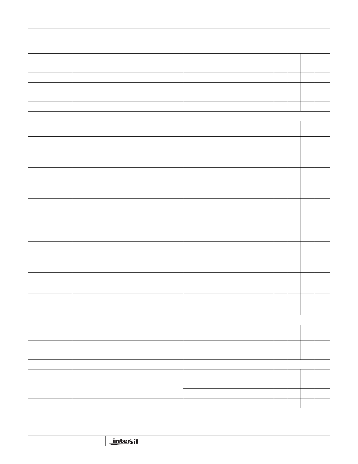
PARAMETER DESCRIPTION CONDITION MIN TYP MAX UNIT
t
SU:DAT
t
LOW
t
HIGH
t
F
t
R
Data Setup Time 250 ns
Clock Low Period 4.7 µs
Clock High Period 4.0 50 µs
Clock/Data Fall Time 300 ns
Clock/Data Rise Time 1000 ns
GENERAL TIMING SPECIFICATIONS (Note 4)
t
1
t
2
t
3
Minimum Setup Time Between VIN Rising above
VUVLO with EN = 1 and SMBus Communications
Minimum Setup Time Between EN Going High with
V
above VUVLO and SMBus Communications
IN
Minimum Time Between VIN Rising above VUVLO
EN = 1, TA = +25°C, VDC capacitor < 10µF 80 µs
> VUVLO, TA= +25°C,
V
IN
VDC capacitor < 10µF
80 µs
EN = 1, TA = +25°C 4.5 ms
with EN = 1 to SMBus BL CTRL On
t
4
t
5
t
6
Minimum Time Between EN Going High with VIN
above VUVLO to SMBus BL CTRL On
Minimum Time for LED Output to Respond to SMBus
Data at any Levels
Response Time Between Backlight CTRL Off with
Boost Not Switching to Backlight CTRL On with
VIN > VUVLO, TA = +25°C 4.5 ms
VIN > VUVLO, EN = 1, TA = +25°C 5 µs
V
> VUVLO, EN = 1, TA = +25°C 5 µs
IN
Boost Switching
t
7
Response Time Between Backlight CTRL On with
Boost Switching to Backlight CTRL Off with Boost
V
> VUVLO, EN = 1, TA = +25°C 5 µs
IN
Not Switching
t
8
t
9
t
10
LED Channel Short Circuit Fault Detection to Status
Register Data Ready
V
to Status Register Data Ready
Short Circuit Detection During Operation
OUT-GND
Time Between VIN Rising Above VUVLO with
EN = 1 and V
Short being Reported in
OUT-GND
VIN > VUVLO, EN = 1, TA = +25°C, LEDs
Active
VIN > VUVLO, EN = 1, TA = +25°C, Fault
FET used
EN = 1, VDC capacitor < 10µF , T
Fault FET used.
= +25°C,
A
6ms
5µs
30 ms
Status Register
t
11
Time Between EN Going High with VIN Above
VUVLO and a V
Status Register
Short being Reported in
OUT-GND
V
> VUVLO, VDC capacitor < 10µF,
IN
T
= +25°C, Fault FET used.
A
30 ms
CURRENT SOURCES
V
headroom
Dominant Channel Current Source Headroom at IIN
I
= 20mA, TA = +25°C 100 mV
LED
Pin
V
RSET
I
LEDmax
Voltage at RSET Pin R
Maximum LED Current Per Channel R
= 36.6kΩ 680 700 720 mV
SET
= 20.9kΩ 35 mA
SET
PWM GENERATOR (Note 4)
FPWM Generated PWM Frequency C
DPWM Duty Cycle of Generated PWM (DC-to-PWM) V
t
MAX_PWM_OFF
Maximum PWMI Off-Time Before Shutdown EN/PWMI toggles 28 ms
= 27nF, C
FPWM
= 0.3V CFPWM = 27nF 90 %
PWMO
= 1.1V CFPWM = 27nF 10 %
V
PWMO
= 220nF 200 Hz
PWMO
6
FN6564.2
December 22, 2008
Page 7
ISL97635A
Electrical Specifications All specifications below are tested at T
otherwise noted. Parameters with MIN and/or MAX limits are 100% tested at +25°C, unless otherwise
= -40°C to +85°C; VIN = 12V, EN = 5V, R
A
= 36.6kΩ, unless
SET
specified. Temperature limits established by characterization and are not production tested. (Continued)
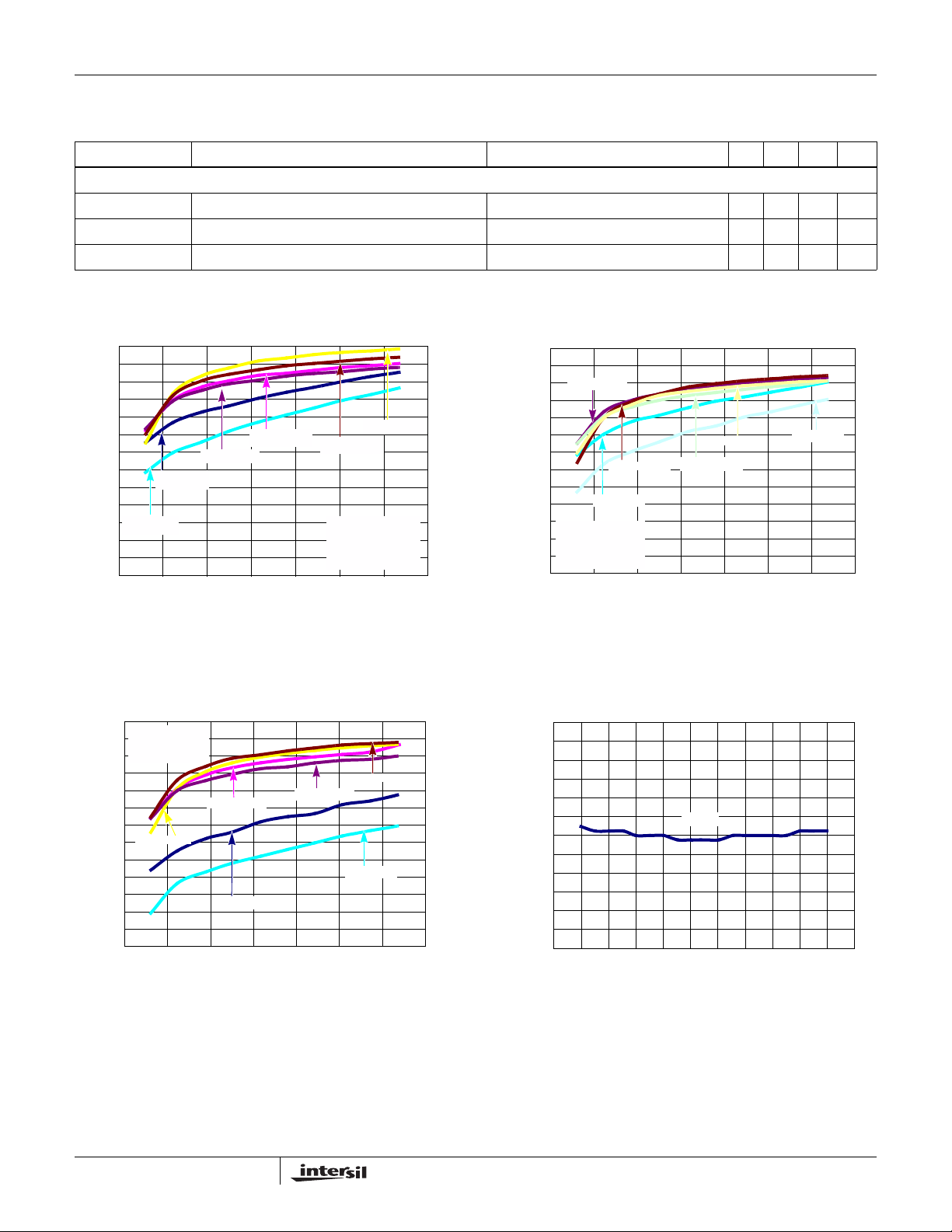
PARAMETER DESCRIPTION CONDITION MIN TYP MAX UNIT
FAULT PIN
I
FAULT
V
FAULT
Fault Pull-down Current VIN = 12V 10 18 30 µA
FAULT Clamp Voltage With Respect to VIN VIN = 12, V
IN
- V
7.5 V
FAULT
IlxStart-up LX Start-up Current VDC = 5.2V 1 2.7 7 mA
Typical Performance Curves
92
90
88
86
84
82
80
78
76
EFFICIENCY (%)
74
72
9S6P - 6V
70
68
66
0 20 40 60 80 100 120 140
9S6P - 12V
7S6P - 6V
7S6P - 12V
(mA)
I
O
7S6P - 18V
9S6P - 18V
L = 8.2µH
IHLP-2525BD-01
DCR = 106mΩ
I
= 3A
SAT
FIGURE 2. EFFICIENCY, L = 8.2µH WITH DCR = 106mΩ,
C
= 4x4.7µF/50V
O
92
90
88
7S6P - 12V
86
84
82
80
78
76
EFFICIENCY (%)
74
72
L = 10µH
70
IHLP-2525BD-01
DCR = 129m
68
I
SAT
66
0 20 40 60 80 100 120 140
7S6P - 6V
= 2.5A
7S6P - 18V
Ω
9S6P - 18V
9S6P - 12V
(mA)
I
O
9S6P - 6V
FIGURE 3. EFFICIENCY, L = 10µH WITH DCR = 129mΩ,
C
= 4x4.7µF/50V
O
92
L = 10µH
90
DCR ~ 500mΩ
<1mm HEIGHT
88
86
84
82
80
7S6P - 18V
78
76
EFFICIENCY (%)
74
72
70
68
66
0 20 40 60 80 100 120 140
7S6P - 12V
7S6P - 6V
I
O
9S6P - 12V
(mA)
9S6P - 18V
9S6P - 6V
FIGURE 4. 3 EFFICIENCY, L = 10µH WITH DCR = 500mΩ,
1mm, C
= 4x4.7µF/50V
O
7
1.2
1.0
0.8
0.6
0.4
0.2
0.0
-0.2
-0.4
-0.6
CURRENT VARIATION (%)
-0.8
-1.0
-1.2
4 6 8 101214161820222426
20mA
V
IN
(V)
FIGURE 5. CURRENT REGULATION
December 22, 2008
FN6564.2
Page 8
Typical Performance Curves (Continued)
ISL97635A
0.020
0.015
0.010
0.005
-0.005
CURRENT MATCHING
-0.010
-0.015
-0.020
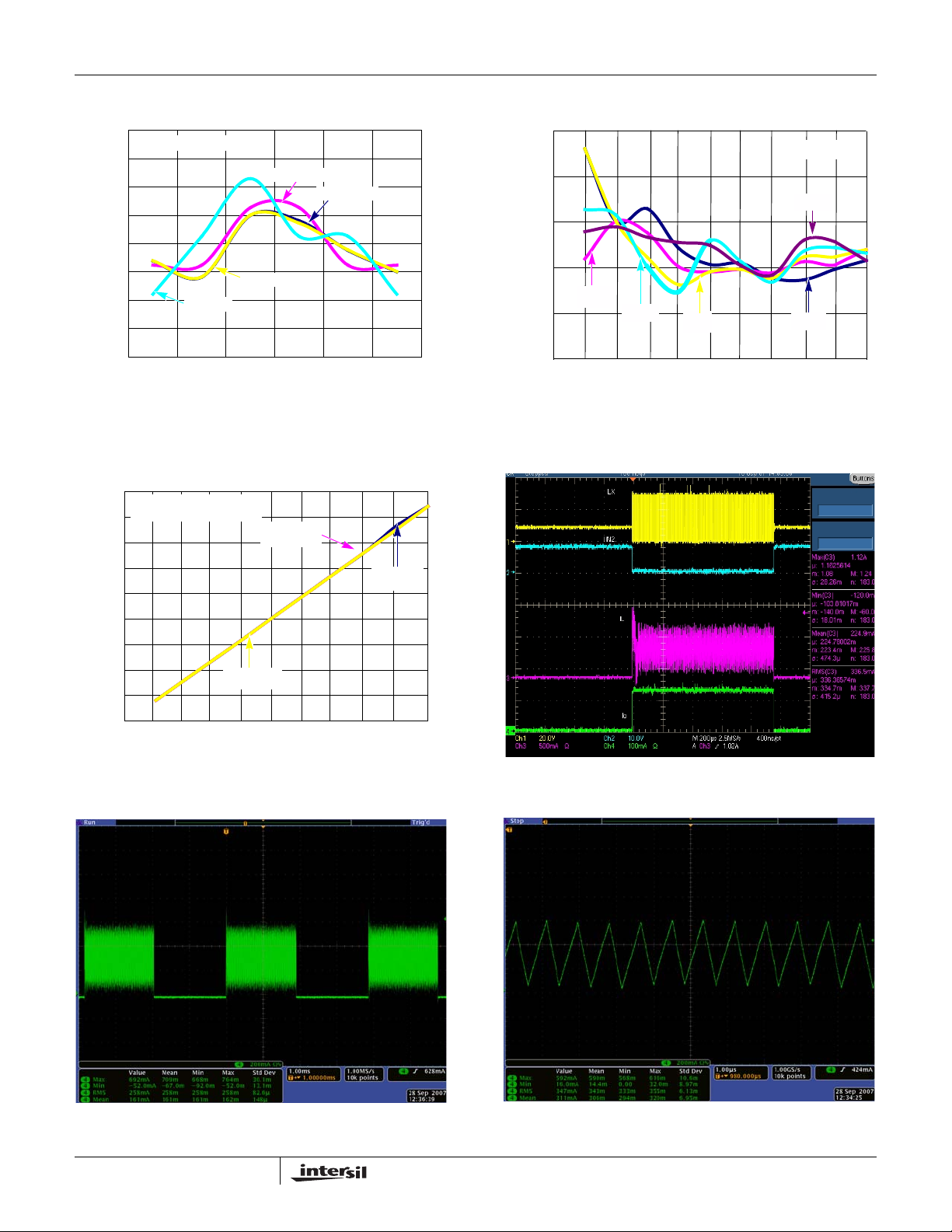
6P9S = 54 LEDs
12V/1mA
12V/20mA
0
6V/20mA
6V/1mA
Ch 0 Ch 1 Ch 2 Ch 3 Ch 4 Ch 5
CHANNELS
FIGURE 6. CHANNEL-TO-CHANNEL CURRENT MATCHING
180
6 CHANNELS
9 LEDs PER CHANNEL
160
140
120
100
80
60
40
TOTAL OUTPUT CURRENT (mA)
20
0
0 102030405060708090100
PWM DUTY CYCLE (%)
VIN = 12V
VIN = 6V
V
= 18V
IN
FIGURE 8. PWM DIMMING LINEARITY
1.0
VIN = 12V
0.9
20kHz
0.8
0.7
CURRENT MATCHING (%)
0.6
0.5
200Hz
10kHz
0 0.1 0.2 0.3 0.4 0.5 0.6 0.7 0.8 0.9 1.0
1kHz
PWM DUTY CYCLE
100Hz
FIGURE 7. CURRENT MATCHING vs DUTY CYCLE vs
DIMMING FREQUENCY
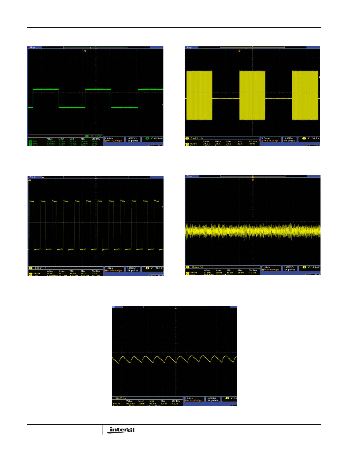
FIGURE 9. LX, IIN, IL AND LO
FIGURE 10. IL AT 50% PWM DIMMING
8
FIGURE 11. I
ZOOM IN AT PWM DIMMING ZOOM IN
L
December 22, 2008
FN6564.2
Page 9
Typical Performance Curves (Continued)
ISL97635A
FIGURE 12. I
FIGURE 14. LX ZOOM IN AT 50% DIMMING
AT 50% PWM DIMMING
LED
FIGURE 13. LX AT 50% PWM DIMMING
FIGURE 15. RIPPLE VOLTAGE
FIGURE 16. RIPPLE VOLTAGE ZOOM IN
9
FN6564.2
December 22, 2008
Page 10
ISL97635A
Pinout
ISL97635A
(24 LD QFN)
TOP VIEW
VDC
VIN
COMP
FAULT
LX
LX
24 23 22 21 20 19
SMBCLK
SMBDAT
FPWM
PWMO
GND
PWMI/EN
1
2
3
4
5
6
789101112
NC
NC
IIN5
IIN4
RSET
IIN3
PGND
18
PGND
17
OVP
16
IIN0
15
IIN1
14
IIN2
13
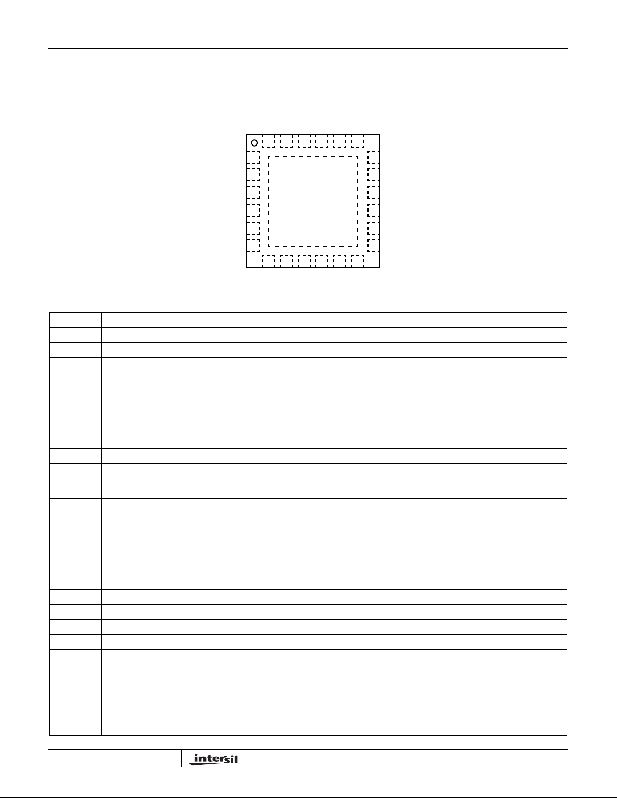
Pin Descriptions (I = Input, O = Output, S = Supply)
PIN NAME TYPE DESCRIPTION
1 SMBCLK I SMBus serial clock input
2 SMBDAT I/O SMBus serial data input and output
3 FPWM I Connect a capacitor between FPWM and GND to set the DPWM frequency. FPWM = 5.4µ/C
If SMBus PWM or DPST mode is used, connect C
connect C
connect C
between V
PWMO
to set the dimming frequency and apply a 0.21V to 1.21V at V
FPWM
and GND pins for DPST operation. If DC-to-PWM mode is used,
PWMO
4 PWMO I/O PWMI buffered output. If one connects a capacitor between PWMO and GND, it forms a lowpass filter
with an internal 40kΩ resistor to filter the PWMI signal for DPST operation when Reg 0x01 = 0x01. If
one applies a 0.2V to 1.2V DC input voltage, the output will be PWM with duty cycle proportional to
the DC input.
5 GND S Analog GND and LED power return
6 PWMI/EN I Dual Functions: Enable Pin and PWM brightness control pin or DPST control input. DO NOT let
PWMI/EN floating. The device needs 4ms for initial power-up Enable, then this pin can be applied with
a PWM signal with off time no longer than 28ms.
7, 8 NC - No Connect. Can be floating or grounded
9 IIN5 I Input 5 to current source, FB, and monitoring
10 IIN4 I Input 4 to current source, FB, and monitoring
11 RSET I Resistor connection for setting LED current, (see Equation 1 for calculating the ILEDmax)
12 IIN3 I Input 3 to current source, FB, and monitoring
13 IIN2 I Input 2 to current source, FB, and monitoring
14 IIN1 I Input 1 to current source, FB, and monitoring
15 IIN0 I Input 0 to current source, FB, and monitoring
16 OVP I Overvoltage protection input
17, 18 PGND S Power ground (LX Power return)
19, 20 LX I Input to boost switch
21 FAULT O Fault disconnect switch
22 COMP O Boost compensation pin
23 VIN S Input voltage for the device and LED power
24 VDC S De-couple capacitor for internally generated supply rail. If 2.7V < VBL+ < 5.5V , apply VDC directly with
a supply voltage of 2.7V to 5.5V
to GND to set the dimming frequency. Also,
FPWM
.
PWMO
FPWM
10
FN6564.2
December 22, 2008
Page 11
ISL97635A
Theory of Operation
PWM Boost Converter
The current mode PWM boost converter produces the
minimal voltage needed to enable the LED stack with the
highest forward voltage drop to run at the programmed
current. The ISL97635A employes current mode control
boost architecture that has a fast current sense loop and a
slow voltage feedback loop. Such architecture achieves a
fast transient response that is essential for the notebook
backlight applications where the power can be a series of
drained batteries or instantly changed to an AC/DC adapter
without rendering a noticeable visual nuisance. The number
of LEDs that can be driven by ISL97635A depends on the
type of LED chosen in the application. The ISL97635A is
capable of boosting up to 34.5V and typically driving 9 LEDs
in series for each of the 6 channels, enabling a total of 54
pieces of the 3.5V/30mA type of LEDs.
Enable and PWMI
The EN/PWMI pin serves dual purposes; it is used as an
enable signal and can be used for PWM input signal for
dimming. If a PWM signal is applied to this pin, the first pulse of
minimum 40µs will be used as an Enable signal. If there is no
signal for longer than 28ms, the device will enter shutdown.
The EN/PWMI pin cannot be floating, thus, a 10kΩ pull-down
resistor may need to be added.
Current Matching and Current Accuracy
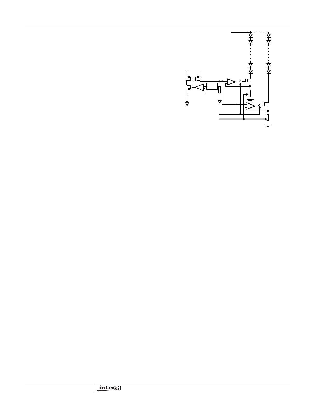
Each channel of the LED current is regulated by the current
source circuit, as shown in Figure 17.
The LED peak current is set by translating the R
to the output with a scaling factor of 733/R
SET
terminals of the current source MOSFETs are designed as
100mV to minimize the power loss. The sources of errors of
the channel-to-channel current matching come from the
op amp’s offset, internal layout, reference, and current
source resistors. These parameters are optimized for current
matching and absolute current accuracy. On the other hand,
the absolute accuracy is additionally determined by the
external R
, and therefore, additional tolerance will be
SET
contributed by the current setting resistor. A 1% tolerance
resistor is therefore recommended.
current
SET
. The source
+
+
-
+
REF
REF
-
RSET
RSET
PWM DIMMING
DC DIMMING
FIGURE 17. SIMPLIFIED CURRENT SOURCE CIRCUIT
-
+
+
-
-
Dynamic Headroom Control
The ISL97635A features a proprietary Dynamic Headroom
Control circuit that detects the highest forward voltage string
or effectively the lowest voltage from any of the IIN pins.
When this lowest I
threshold, V
SC
voltage is lower than the short circuit
IN
, such voltage will be used as the feedback
signal for the boost regulator. The boost makes the output to
the correct level such that the lowest IIN pin is at the target
headroom voltage. Since all LED stacks are connected to
the same output voltage, the other IIN pins will have a higher
voltage, but the regulated current source circuit on each
channel will ensure that each channel has the same
programmed current. The output voltage will regulate cycle
by cycle and it is always referenced to the highest forward
voltage string in the architecture.
Dimming Controls
The ISL97635A allows two ways of controlling the LED
current, and therefore, the brightness. They are:
1. DC current adjustment.
2. PWM chopping of the LED current defined in Step 1.
There are various ways to achieve DC or PWM current
control, which will be described in the following.
MAXIMUM DC CURRENT SETTING
The initial brightness should be set by choosing an
appropriate value for R
maximum possible LED current, as shown in Equation 1:
733
I
LEDmax
=
---------------
R
SET
. This should be chosen to fix the
SET
(EQ. 1)
11
DC CURRENT ADJUSTMENT
Once R
is fixed, the LED DC current can be adjusted
SET
through register 0x07 (BRTDC), as shown in Equation 2:
I
LED
2.87 BRTDC R
⁄×=
SET
(EQ. 2)
FN6564.2
December 22, 2008
Page 12

ISL97635A
BRTDC can be programmed from 0 to 255 in decimal and
defaults to 255 (0xFF). If left at the default value, LED
current will be fixed at I
. BRTDC can be adjusted
LEDmax
dynamically on the fly during operation. BRTDC = 0
disconnects all channels and ILED is guaranteed to be
<10µA at this state.
For example, if the maximum required LED current (I
LEDmax
is 20mA, rearranging Equation 1 yields Equation 3:
R
733 0.02⁄ 36.6kΩ==
SET
(EQ. 3)
If BRTDC is set to 200, then:
2.87∗200 36600⁄ 15.7mA==
I
LED
(EQ. 4)
PWM CONTROL
The ISL97635A provides four different PWM dimming
methods, as described in the following. Each of these
methods results in PWM chopping of the current in the LEDs
for all 6 channels to provide an average LED current. During
the on-periods, the LED current will be defined by the value
of R
and BRTDC, as described in Equations 1 and 2. The
SET
source of the PWM signal can be described as follows:
1. Internally generated 256 step duty cycle programmed
through the SMBus.
2. External signal from PWMI.
3. DPST mode. Internally generated signal with a duty cycle
defined by the product of the external PWMI and SMBus
programmed PWM at the internal setting frequency.
4. DC-to-PWM control.
The default PWM dimming is in DPST mode. In all four
methods, the average LED current of each channel is
controlled by I
and the PWM duty cycle in percent as
LED
shown in Equation 5:
I
LED ave()ILED
PWM×=
(EQ. 5)
Method 1 (Internal Mode, SMBus controlled PWM)
The average LED current of each channel is controlled by the
internally generated PWM signal as shown in Equation 6:
I
LED ave()ILED
BRT 255⁄()×=
(EQ. 6)
where BRT is the PWM brightness level programmed in the
register 0x00. BRT ranges from 0 to 255 in decimal and
defaults to 255 (0xFF). BRT = 0 disconnects all channels
and I
is guaranteed to be <10µA in this state.
LED
To use only the SMBus controlled PWM brightness control,
users need to set Register 0x01 to 0x05 with EN/PWMI in
logic high.
The SMBus controlled PWM frequency is adjusted by a
capacitor at the FPWM pin, which will be described in “PWM
Dimming Frequency Adjustment” on page 13.
Method 2 (External Mode)
The average LED current of each channel can also be
controlled by an external PWMI signal, as shown in Equation 7:
)
I
LED ave()ILED
PWMI×=
(EQ. 7)
The PWM dimming frequency can be for example 20kHz but
there are a minimum on and off time requirements such that
the dimming will be in the range of 10% to 99.5%. If the
dimming frequency is below 5kHz, the dimming range can
be 1% to 99.5%.
The PWM dimming off time cannot be longer than 28ms or
else the driver will enter shutdown.
To use PWMI only brightness control, users need to set
Register 0x01 to 0x03.
Method 3 (DPST Mode)
The average LED current of each channel can also be
controlled by the product of the SMBus controlled PWM and
the external PWMI signals as follows:
I
LED ave()ILED
=
xPWM
DPST
(EQ. 8)
Where:
PWM
DPST
BRT 255⁄ PWMI×=
(EQ. 9)
Therefore:
I
LED ave()ILED
BRT 255⁄× PWMI×=
(EQ. 10)
Where BRT is the value held in register 0x00 (default setting
0xFF) controlled by SMBus and PWMI is the duty cycle of
the incoming PWMI signal. In this way, the users can change
the PWM current in ratiometric manner to achieve DPST
compliance backlight dimming.
To use the DPST mode, users need to set register 0x01 to
0x01 with the external PWM signal.
The DPST mode PWM frequency is adjusted by a capacitor
at the FPWM pin. Also, a C
capacitor is also needed,
PWMO
which will be described in “PWM Dimming Frequency
Adjustment” on page 13.
For example, if the SMBus controlled PWM duty is 80%
dimming at 200Hz (see C
in Equation 10) and the
FPWM
external PWMI duty cycle is 60% dimming at 1kHz, the
resultant PWM duty cycle is 48% dimming at 200Hz.
Method 4 (Analog Mode, DC-to-PWM Mode)
By overdriving the PWMO pin with a DC voltage between
0.21V and 1.21V, the average LED current of each channel
12
FN6564.2
December 22, 2008
Page 13

ISL97635A
is controlled by the internally generated PWM signal as
shown in Equation 11:
I
LED ave()ILED
BRT 255 1 V PWMO()0.21–()–()×⁄×=
(EQ. 11)
Where BRT is the value held in regist er 0x00 (def ault settin g
0xFF). The PWMO pin is internally driven to 0.21V via a
40kΩ resistor when the PWMI/EN pin is in logic high, any
overdrive circuit will need to be able to drive up to 40µA in
order to overcome this.
The DC-to-PWM controlled PWM frequency is adjusted by a
capacitor at the FPWM pin, which will be described in “PWM
Dimming Frequency Adjustment” on page 13.
For example, if PWMO is applied with a DC voltage ≥1.21V,
the output will be zero. On the other hand, if the PWMO is
applied with a DC voltage ≤ 0.21V, the PWM duty cycle will
be at its maximum. If the PWMO pin is applied with a DC
voltage of 0.31V, the PWM duty cycle will be at 90% at
200Hz if C
FPWM
= 27nF.
PWM Dimming Frequency Adjustment
(Applicable to SMBus controlled PWM, DPST, and
DC-to-PWM Modes)
Except for the external PWM dimming mode where the
frequency follows the external signal’s, the dimming
frequencies of the other modes are set by an external
capacitor C
C
FPWM
at the FPWM pin as shown in Equation 12:
FPWM
5.4μ F
⁄=
PWM
(EQ. 12)
Switching Frequency
An internal clock of 1.2MHz is used for the boost regulator
control of the LX pin in default. There are 2 levels of
switching frequencies: 600kHz or 1.2MHz. Each can be
programmed in the Configuration Register 0x08 bit 2. The
default switching frequency is at 1.2MHz.
5V Low Dropout Regulator
A 5.2V LDO regulator is present at the VDC pin to develop
the necessary low voltage supply which is used by the chips
internal control circuitry. Because VDC is an LDO pin, it
requires a bypass capacitor of 1µF or more for the
regulation. For applications with an input voltage ≤ 5.5V, the
VIN and VDC pins can be connected together. The VDC pin
can be used as a coarse reference with few mA sourcing
capability.
In-rush Control and Soft-start
The ISL97635A has separately built-in independent inrush
control and soft-start functions. The inrush control function is
built around the short circuit protection FET, and is only
available in applications which include this device. At
start-up, the fault protection FET is turned on slowly due to a
30µA pull-down current output from the FAULT pin. This
discharges the fault FET's gate-source capacitance, turning
on the FET in a controlled fashion. As this happens, the
output capacitor is charged slowly through the weakly turned
on FET before it becomes fully enhanced. This results in a
low in-rush current. This current can be further reduced by
adding a capacitor (in the 1nF to 5nF range) across the
gate-source terminals of the FET.
where F
For example, if FPWM = 200Hz, C
is the desirable PWM dimming frequency.
PWM
= 5.4µ/200 = 27nF
FPWM
The PWM dimming frequency can be for example 20kHz but
there are a minimum on and off time requirements such that
the dimming will be in the range of 10% to 99.5%. If the
dimming frequency is below 5kHz, the dimming range can
be 1% to 99.5%.
In the DPST and DC-to-PWM modes, a C
also needed. An internal 40kΩ and an external C
PWMO
capacitor is
at the
PWMO
PWMO pin form a low pass network to filter the PWMI to an
averaged DC. As a result, the time constant of the 40kΩ and
C
should be significantly larger than the external PWMI
PWMO
period, t, such that:
40kΩ x C
For example, if F
PWMO
>t
PWM
or above, a 220nF C
is 200Hz and external PWMI is 1kHz
can be chosen that allows the
PWMO
(EQ. 13)
external PWMI signal to be filtered as an averaged DC. Also,
the F
frequency in the DPST mode should be limited
PWM
between 100Hz to 2kHz and at least five times smaller than
the external PWMI frequency when DPST mode is used.
Once the chip detects that the fault protection FET is turned
on hard, it is assumed that inrush is complete. At this point,
the boost regulator will begin to switch and the current in the
inductor will ramp-up. The current in the boost power switch
is monitored and the switching terminated in any cycle
where the current exceeds the current limit. The ISL97635A
includes a soft-start feature where this current limit starts at a
low value (375mA). This is stepped up to the final 3A current
limit in seven further steps of 375mA. These steps will
happen over a 1ms total time, such that after 1ms the final
limit will be reached. This allows the output capacitor to be
charged to the required value at a low current limit and
prevents high input current for systems that have only a low
to medium output current requirement.
For systems with no master fault protection FET, the in-rush
current will flow towards C
determined by the ramp rate of VIN and the values of C
when VIN is applied and it is
OUT
OUT
and L.
13
FN6564.2
December 22, 2008
Page 14

ISL97635A
Fault Protection and Monitoring
The ISL97635A features ex te nsive protection functions to
cover all the perceivable failure conditions. The failure mode
of a LED can be either open circuit or as a short. The
behavior of an open circuited LED can additionally take the
form of either infinite resistance or, for some LEDs, a zener
diode, which is integrated into the device in parallel with the
now opened LED.
For basic LEDs (which do not have built-in zener diodes), an
open circuit failure of an LED will only result in the loss of
one channel of LEDs without affecting other channels.
Similarly, a short circuit condition on a channel that results in
that channel being turned off does not affect other channels
unless a similar fault is occurring. All LED faults are reported
via the SMBus interface to register 0x02 (Fault/Status
register). The controller is able to determine which channels
have failed via register 0x09 (Output masking register). The
controller can also choose to use register 0x09 to disable
faulty channels at start-up, resulting in only further faulty
channels being reported by register 0x02.
Due to the lag in boost response to any load change at its
output, certain transient events (such as LED current steps
or significant step changes in LED duty cycle) can transiently
look like LED fault modes. The ISL97635A uses feedback
from the LEDs to determine when it is in a stable operating
region and prevents apparent faults during these transient
events from allowing any of the LED stacks to fault out. See
Table 1 for more details.
A fault condition that results in an input current that exceeds
the devices electrical limits will result in a shutdown of all
output channels. The control device logic will remain
functional such that the Fault/Status Register can be
interrogated by the system. The root cause of the failure will
be loaded to the volatile Fault/Status Register so that the
host processor can interrogate the data for failure
monitoring.
Short Circuit Protection (SCP)
The short circuit detection circuit monitors the voltage on
each channel and disables faulty channels which are
detected above the programmed short circuit threshold.
There are two selectable levels of short circuit threshold
(3.1V and 8.0V) that can be programmed through the
Configuration Register 0x08 bit 0. When an LED becomes
shorted, the action taken is described in T able 1. The default
short circuit threshold is 8V. The detection of this failure
mode can be disabled via register 0x08 bit 1 if required.
Open Circuit Protection (OCP)
When one of the LEDs becomes open circuit, it can behave
as either an infinite resistance or a gradually increasing finite
resistance. The ISL97635A monitors the current in each
channel such that any string which reaches at least 75% of
the intended output current is considered “good”. Should the
current subsequently fall below 50% of the target, the
channel will be considered an “open circuit”. Furthermore,
should the boost output of the ISL97635A reach the OVP
limit or should the lower over-temperature threshold be
reached, all channels which are not “good” will immediately
be considered as “open circuit”. Detection of an “open
circuit” channel will result in a time-out before disabling of
the affected channel. This time-out is sped up when the
device is above the lower over-temperature threshold in an
attempt to prevent the upper over-temperature trip point from
being reached.
Some users employ some special types of LEDs that have
zener diode structure in parallel with the LED for ESD
enhancement and enabling open circuit operation. When
this type of LED is open circuited, the effect is as if the LED
forward voltage has increased but no lighting. Any affected
string will not be disabled, unless the failure results in the
boost OVP limit being reached, allowing all other LEDs in the
string to remain functional. Care should be taken in this case
that the boost OVP limit and SCP limit are set properly, so as
to make sure that multiple failures on one string do not
cause all other good channels to be faulted out. This is due
to the increased forward voltage of the faulty channel making
all other channels look as if they have LED shorts. See
Table 1 for details regarding responses to fault conditions.
Overvoltage Protection (OVP)
The integrated OVP circuit monitors the output voltage and
keeps the voltage at a safe level. The OVP threshold is set
as Equation 14:
OVP 1.21V R
+()R
UPPERRLOWER
⁄×=
LOWER
(EQ. 14)
These resistors should be large to minimize the power loss.
For example, a 1MΩ R
to 32.2V. Large OVP resistors also allow C
UPPER
and 39kΩ R
LOWER
discharges
OUT
sets OVP
slowly during the PWM off time.
Undervoltage Lockout
If the input voltage falls below the UVLO level of 2.45V, the
device will stop switching and reset. Operation will restart
when the voltage comes back into the operating range.
Input Overcurrent Protection
During normal switching operation, the current through the
internal boost power FET is monitored. If the current
exceeds the current limit, the internal switch will be turned
off. This monitoring happens on a cycle-by-cycle basis in a
self protecting way.
Additionally, the ISL97635A monitors the voltage at the LX
and OVP pins. At start-up, a fixed current is injected out of
the LX pins and into the output capacitor. The device will not
start-up unless the voltage at LX exceeds 1.2V . Furthermore,
should the voltage at LX not rise above this threshold during
any subsequent period where the power FET is not switched
on, it will immediately disable the input protection FET. The
OVP pin is also monitored such that if it rises above and
14
FN6564.2
December 22, 2008
Page 15
ISL97635A
subsequently falls below 20% of the target OVP level, the
input protection FET will also be switched off.
Over-Temperature Protection (OTP)
The ISL97635A includes two over-temperature thresholds.
The lower threshold is set to +130°C. When this threshold is
reached, any channel which is outputting current at a level
significantly below the regulation target will be treated as
“open circuit” and disabled after a time-out period. This
time-out period is also reduced to 800µs when it is above the
lower threshold. The intention of the lower threshold is to
allow bad channels to be isolated and disabled before they
cause enough power dissipation (as a result of other
channels having large voltages across them) to hit the upper
temperature threshold.
VIN
IMAX
DRIVER
ILIMIT
FAULT
LOGIC
O/P
SHORT
FET
DRIVER
The upper threshold is set to +150°C. Each time this is
reached, the boost will stop switching and the output current
sources will be switched off. Once the device has cooled to
approximately +100°C, the device will restart with the DC
LED current level reduced to 77% of the initial setting. If the
dissipation problem persists, subsequent hitting of the limit
will cause identical behavior, with the current reduced in
steps to 53% and finally 30%. Hitting of the upper threshold
will also set the thermal fault bit of the Fault/Status register
0x02. Unless disabled via the EN pin, the device stays in an
active state throughout, allows the external processor to
interrogate the fault condition.
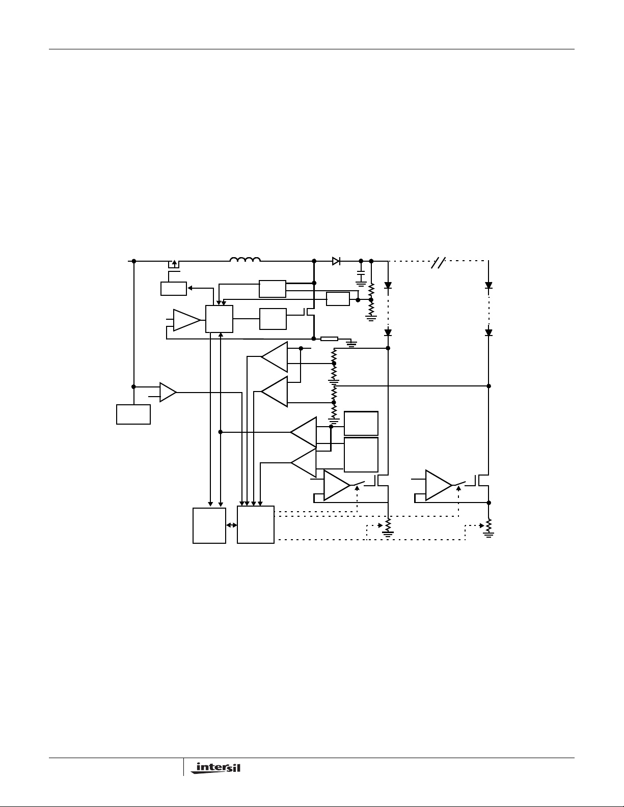
For the extensive fault protection conditions, please refer to
Figure 18 and Table 1 for details.
LX
LX
VSC
VSC
OVP
VOUT
IIN0
REG
VSET/2
THRM
THRM
SHDN
SHDN
OTP
OTP
+
-
DC CURRENT
FAULT/
STATUS
REGISTER
SMBUS
CONTROL
LOGIC
VSET
PWM/OC0/SC0
FIGURE 18. SIMPLIFIED FAULT PROTECTIONS
REF
T2
TEMP
SENSOR
T1
VSET
Q0
PWM/OC5/SC5
IIN5
+
-
Q5
15
FN6564.2
December 22, 2008
Page 16

DETECTION
CASE FAILURE MODE
1 CH0 Short Circuit Upper
2 CH0 Short Circuit Upper OTP
3 CH0 Short Circuit Upper OTP not
4 CH0 Open Circuit
with infinite
resistance
5 CH0 LED Open
Circuit but has
paralleled Zener
6 CH0 LED Open
Circuit but has
paralleled Zener
7 CH0 LED Open
Circuit but has
paralleled Zener
8 Channel-to-Channel
ΔVF too high
9 Channel-to-Channel
ΔVF too high
10 Output LED stack
voltage too high
11 VOUT/LX shorted to
GND
MODE FAILED CHANNEL ACTION GOOD CHANNELS ACTION
Over-Temperature
Protection limit
(OTP) not
triggered and
VIIN0 < VSC
triggered but VIN0
< VSC
triggered but
VIIN0 > VSC
Upper OTP not
triggered and
VIIN0 < VSC
Upper OTP not
triggered and
VIIN0 < VSC
Upper OTP
triggered but
VIIN0 < VSC
Upper OTP not
triggered but
VIIN0 > VSC
Upper OTP not
triggered but VIINx
> VSC
Lower OTP
triggered but VIINx
< VSC
Upper OTP
triggered but VIINx
< VSC
VOUT > VOVP Driven with normal current. Any channel that is below 50% of the target
LX current and
timing are
monitored.
ISL97635A
TABLE 1. PROTECTIONS TABLE
VOUT
REGULATED BY
CH0 ON and burns power CH1 through CH5 Normal Highest VF of CH1
CH0 goes off until chip cooled and
then comes back on with current
reduced to 76%. Further OTP
triggers result in reduction to 53%,
then 30%. Thermal event reported
in Fault/Status Register.
CH0 doubled after 6ms time-out.
Time-out reduced to 420µs if above
lower OTP limit
VOUT will ramp to OVP. CH0 will
time-out after 6ms (800µs if above
lower OTP limit) and switch off.
VOUT will drop to normal level.
CH0 remains ON and has highest
VF, thus VOUT increases
CH0 goes off until chip cooled and
then comes back on with current
reduced to 76%. Further OTP
triggers result in reduction to 53%,
then 30%. Thermal event reported
in Fault/Status Register.
CH0 OFF CH1 through CH5 Normal Highest VF of CH1
CH0 remains ON and has highest
VF, thus VOUT increases.
Any channel at below 50% of the target current will fault out after 400µs.
Remaining channels driven with normal current.
All channels switched off until chip cooled and then comes back on with
current reduced to 76%. Further OTP triggers result in reduction to 53%,
then 30%. Thermal event reported in Fault/Status Register.
current will time-out after 6ms.
Fault switch disabled and system shutdown until fault goes away, VOUT
is checked at startup with a low current from LX to check for presence of
short before the fault switch is enabled.
Same as CH0 Highest VF of CH1
CH1 through CH5 Normal Highest VF of CH1
CH1 through CH5 Normal Highest VF of CH1
CH1 through CH5 ON, Q1 through
Q5 burn power
Same as CH0 VF of CH0
VOUT increases then CH-X
switches OFF . This is an unwanted
shut off and can be prevented by
setting OVP and/or VSC at an
appropriate level.
through CH5
through CH5
through CH5
through CH5
VF of CH0
through CH5
VF of CH0
Highest VF of CH0
through CH5
Highest VF of CH0
through CH5
Highest VF of CH0
through CH5
OVP pin
monitored for
excursions below
20% of OVP
threshold
16
FN6564.2
December 22, 2008
Page 17
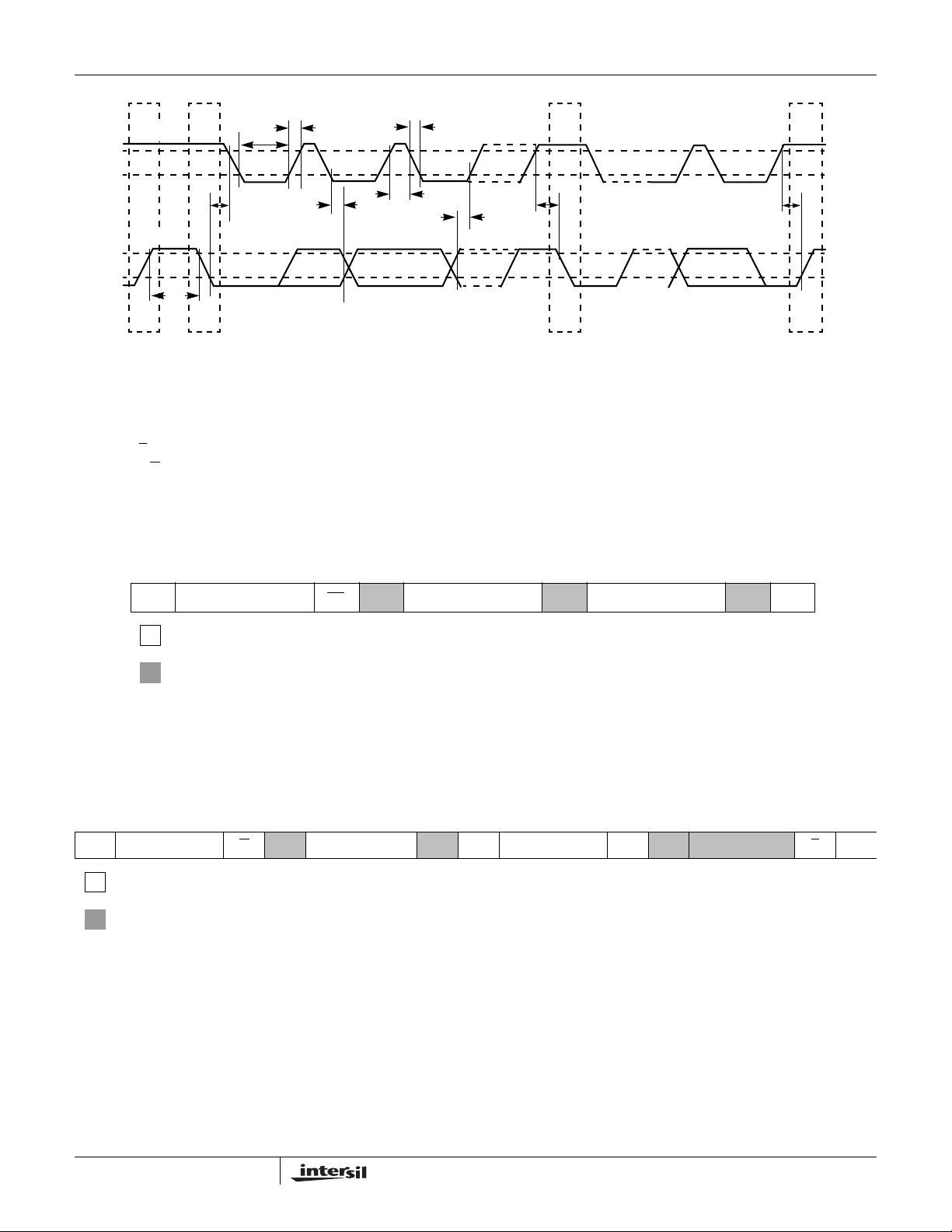
ISL97635A
t
HIGH
t
F
t
t
SU:DAT
SU:STA
t
SU:STO
V
V
IH
IL
SMBCLK
t
HD:STA
t
LOW
t
R
t
HD:DAT
SMBDAT
V
IH
V
IL
t
BUF
SSP
NOTES:
SMBus Description
S = start condition
P = stop condition
A = acknowledge
A
= not acknowledge
R/W
= read enable at high; write enable at low
FIGURE 19. SMBUS INTERFACE
171181811
P
S
SLAVE ADDRESS W A COMMAND CODE A DATA BYTE AP
Master to Slave
Slave to Master
FIGURE 20. WRITE BYTE PROTOCOL
1711811811811
S SLAVE ADDRES S W A COMMAND CODE A S SLAV E ADDRESS R A DATA BYTE A P
Master to Slave
Slave to Master
FIGURE 21. READ BYTE PROTOCOL
17
FN6564.2
December 22, 2008
Page 18
ISL97635A
Write Byte
The Write Byte protocol is only three bytes long. The first byte
starts with the slave address followed by the “command code,”
which translates to the “register index” being written. The third
byte contains the data byte that must be written into the register
selected by the “command code”. A shaded label is used on
cycles during which the slaved backlight controller “owns” or
“drives” the Data line. All other cycles are driven by the “host
used in other backlight controller specifications to avoid
confusion. Therefore, if the device is in the write mode where bit
0 is 0, the slave address byte is 0x58 or 0101 1000b. If the
device is in the read mode where bit 0 is 1, the slave address
byte is 0x59 or 01011001b.
The backlight controller may sense the state of the pins at POR
or during normal operation—the pins will not change state while
the device is in operation.
master.”
Read Byte
MSB
As shown in the Figure 21, the 4 byte long Read Byte protocol
starts out with the slave address followed by the “command
code” which translates to the “register index.” Then the bus
direction turns around with the re-broadcast of the slave
address with bit 0 indicating a read (“R”) cycle. The fourth byte
contains the data being returned by the backlight controller.
That byte value in the data byte reflects the value of the register
being queried at the “command code” index. Note the bus
directions, which are highlighted by the shaded label that is
used on cycles during which the slaved backlight controller
“owns” or “drives” the Data line. All other cycles are driven by
the “host master.”
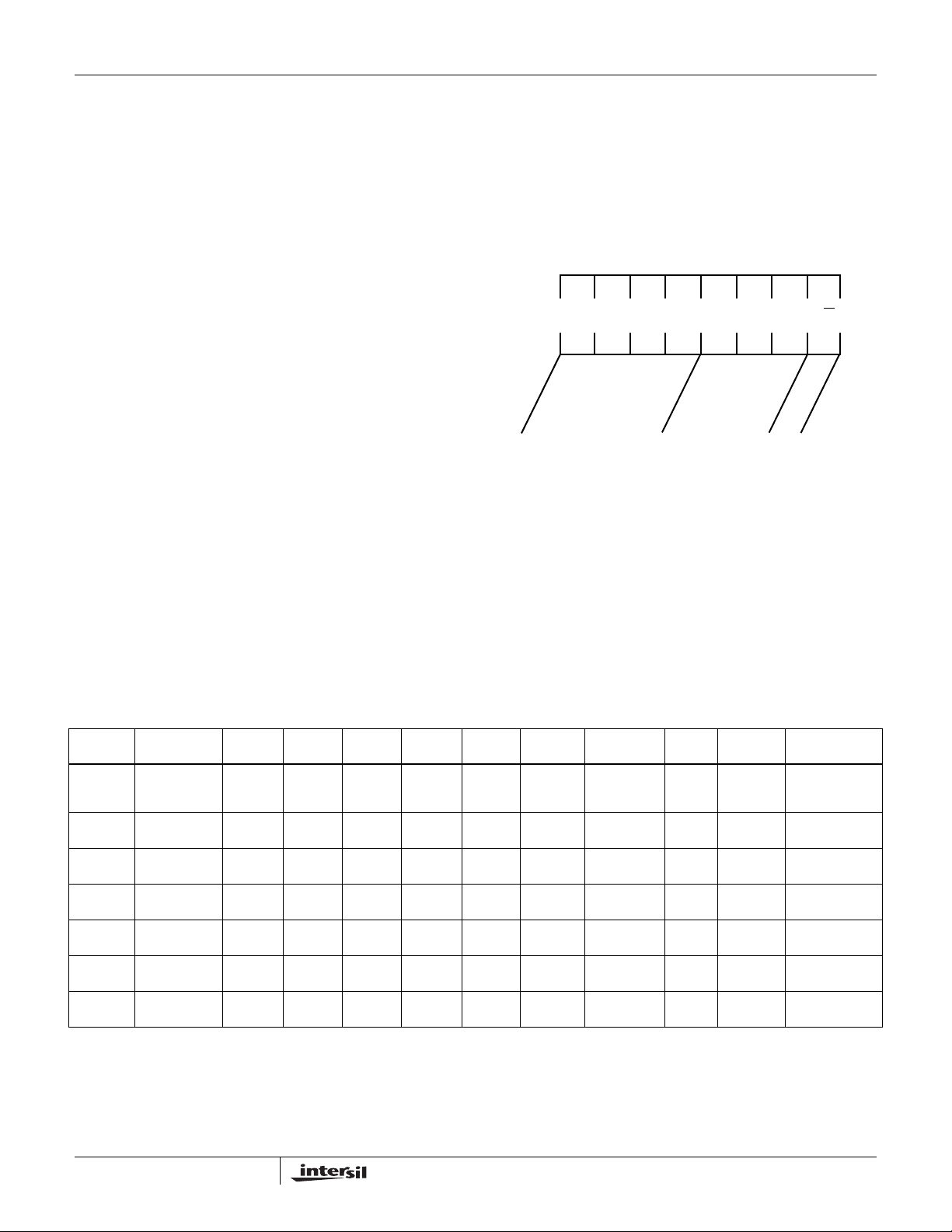
Slave Device Address
The slave address contains in 7 MSB plus one LSB as R/W bit
but these 8 bits are usually called slave address byte. As
SMBus Register Definitions
The backlight controller registers are Byte wide and
accessible via the SMBus Read/Write Byte protocols. Their
bit assignments are provided in the following sections with
reserved bits containing a default value of “0”.
shown in Figure 22, the high nibble of the slave address byte is
0x5 or 0101b to denote the “backlight controller class.” Bit 3 in
the lower nibble of the slave address byte is 1. Bit 0 is always
the R/W bit, as specified by the SMBus protocol. Note: In this
document, the device address will always be expressed as a
full 8-bit address instead of the shorter 7-bit address typically
TABLE 2A. REGISTER LISTING
ADDRESS REGISTER BIT 7 BIT 6 BIT 5 BIT 4 BIT 3 BIT 2 BIT 1 BIT 0
0x00 PWM
0x01 Device Control
0x02 Fault/Status
0x03 Identification
0x07 DC Brightness
0x08 Configuration
0x09 Output Channel
Brightness
Control Register
Register
Register
Register
Control Register
Register
Register
BRT7 BRT6 BRT5 BRT4 BRT3 BRT2 BRT1 BRT0 0xFF Read and Write
Reserved Reserved Reserved Reserved Reserved PWM_MD PWM_SEL BL_CTL 0x00 Read and Write
Reserved Reserved 2_CH_SD 1_CH_SD BL_STAT OV_CURR THRM_SHDN FAULT 0x00 Read Only
LED
PANEL
BRTDC7 BRTDC6 BRTDC5 BRTDC4 BRTDC3 BRTDC2 BRTDC1 BRTDC0 0xFF Read and Write
Reserved Reserved Reserved Reserved Reserved FSW VSC1 VSC0 0xXF Read and Write
Reserved Reserved CH5 CH4 CH3 CH2 CH1 CH0 0xFF Read and Write
MFG3 MFG2 MFG1 MFG0 REV2 REV1 REV0 0xC8 Read Only
0101100R/W
DEVICE
IDENTIFIER
FIGURE 22. SLAVE ADDRESS BYTE DEFINITION
DEVICE
ADDRESS
DEFAULT
VALUE
LSB
E
T
I
R
W
/
D
A
E
R
PROTOCOL
T
I
B
SMBUS
18
FN6564.2
December 22, 2008
Page 19
ISL97635A
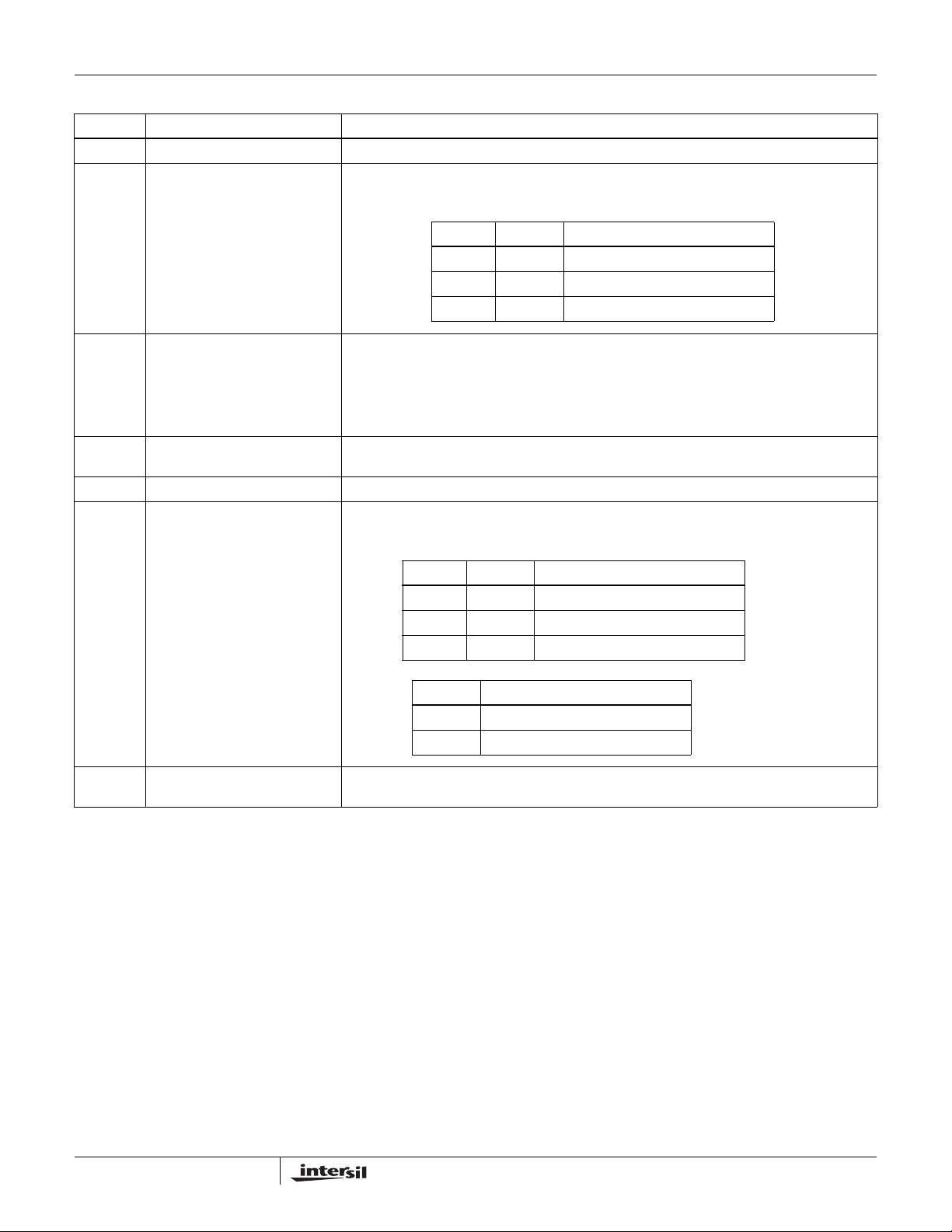
TABLE 2B. DATA BIT DESCRIPTIONS
ADDRESS REGISTER DATA BIT DESCRIPTIONS
0x00 PWM Brightness Control Register BRT[7..0] = 256 steps of DPWM duty cycle brightness control
0x01 Device Control Register PWM_MD = PWM mode select bit (1 = absolute brightness, 0 = % change), default = 0
PWM_SEL = Brightness control select bit (1 = control by PWMI, 0 = control by SMBus), default = 0
BL_CTL = BL On/Off (1 = On, 0 = Off), default = 0
PWM_MD PWM_SEL MODE
X 1 PWMI Mode
1 0 SMBus Mode
0 0 SMBus and PWMI mode with DPST
0x02 Fault/Status Register 2_CH_SD = Two LED output channels are shutdown (1 = shutdown, 0 = OK)
1_CH_SD = One LED output channel is shutdown (1 = shutdown, 0 = OK)
BL_STAT = BL status (1 = BL On, 0 = BL Off)
OV_CURR = Input overcurrent (1 = Overcurrent condition, 0 = Current OK)
THRM_SHDN = Thermal Shutdown (1 = Thermal fault, 0 = Thermal OK)
FAULT = Fault occurred (Logic “OR” of all of the fault conditions)
0x03 Identification Register MFG[3..0] = Manufacturer ID (16 vendors available. Intersil is vendor ID 9)
REV[2..0] = Silicon rev (Rev 0 through Rev 7 allowed for silicon spins)
0x07 DC Brightness Control Register BRTDC[7..0] = 256 steps of DC brightness control
0x08 Configuration Register VSC[1..0] = Short circuit thresholds selection
FSW[2] = Switching frequencies selection
VSC1 VSC0 OPERATION
0 X No VSC error detection
1 0 VSC = 3.1V ±15%
1 1 VSC = 8V ±15%
FSW OPERATION
0x09 Output Channel Mask / Fault
Readout Register
CH[5..0] = Output Channel Read and Write. In Write, 1 = Channel Enabled, 0 = Channel Disabled.
In Read, 1 = Channel OK, 0 = Channel Not OK/Channel disabled
PWM Brightness Control Register (0x00)
The Brightness control resolution has 256 steps of PWM
duty cycle adjustment. The bit assignment is shown in
Figure 23. All of the bits in this Brightness Control Register
can be read or write. Step 0 corresponds to the minimum
step where the current is less than 10µA. Step1 to step 255
represent the linear steps between 0.39% and 100% duty
cycle with approximately 0.39% duty cycle adjustment per
step.
• An SMBus Write Byte cycle to register 0x00 sets the PWM
brightness level only if the backlight controller is in SMBus
0F
1F
= 600kHz
SW
= 1.2MHz
SW
• An SMBus Read Byte cycle to register 0x00 returns the
• An SMBus setting of 0xFF for register 0x00 sets the
• An SMBus setting of 0x00 for register 0x00 sets the
• Default value for register 0x00 is 0xFF.
mode (see Table 3 Operating Modes selected by Device
Control Register Bits 1 and 2).
programmed PWM brightness level regardless of the
value of PWM_SEL.
backlight controller to the maximum brightness.
backlight controller to the minimum brightness output in
which the LED current is guaranteed to be less than 10µA.
19
FN6564.2
December 22, 2008
Page 20
ISL97635A
Device Control Register (0x01)
This register has two bits that control the operating mode of
the backlight controller and a single bit that controls the BL
ON/OFF state. The remaining bits are reserved. The bit
assignment is shown in Figure 24. All other bits in the Device
Control Register will read as low unless otherwise written.
Bits 7 and 6 are not implemented and will always read low.
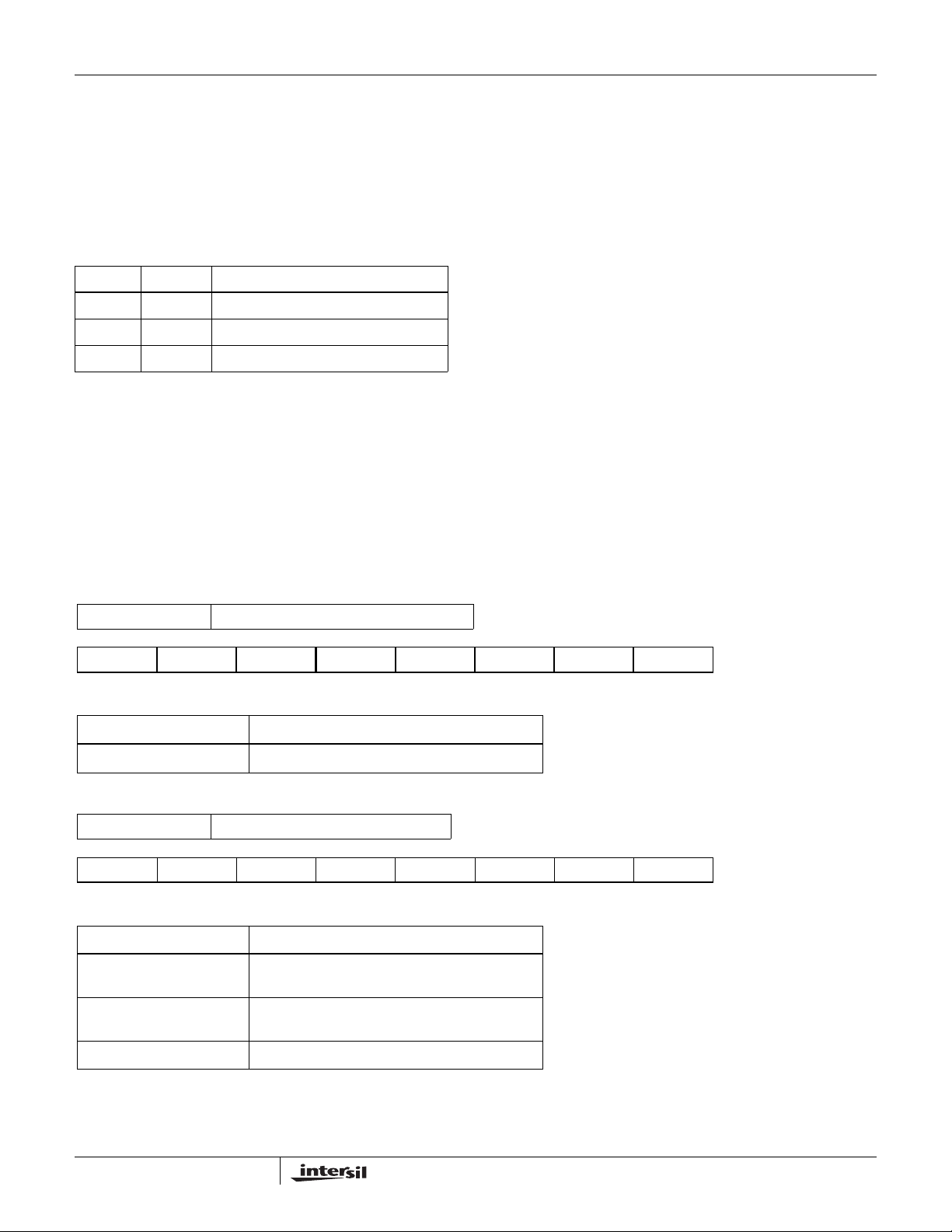
TABLE 3. OPERATING MODES SELECTED BY DEVICE
CONTROL REGISTER BITS 1 AND 2
PWM_MD PWM_SEL MODE
X 1 PWMI Mode
1 0 SMBus Mode
0 0 SMBus and PWMI Mode with DPST
The PWM_SEL bit determines whether the SMBus or PWMI
input should drive the output br ig h tness in terms of PWM
dimming. When PWM_SEL bit is 1, the PWMI drives the
output brightness regardless of what the PWM_MD is.
When the PWM_SEL bit is 0, the PWM_MD bit selects the
manner in which the PWM dimming is to be interpreted;
when this bit is 1, the PWM dimming is based on the SMBus
brightness setting. When this bit is 0, the PWM dimming
reflects a percentage change in the current brightness
programmed in the SMBus register 0x00, i.e. DPST (Display
Power Saving Technology) mode as shown in Equation 15:
DPST Brightness Cbt PWMI×=
(EQ. 15)
Where:
Cbt = Current brightness setting from SMBus register 0x00
without influence from the PWMI
PWMI = is the percent duty cycle of the PWMI
For example, the Cbt = 50% duty cycle programmed in the
SMBus register 0x00 and the PWM frequency is tuned to be
200Hz with an appropriate capacitor at the FPWM pin. On the
other hand, PWMI is fed with a 1kHz 30% high PWM signal.
When PWM_SEL = 0 and PWM_MD = 0, the device is in DPST
operation where DPST brightness = 15% PWM dimming at
200Hz.
• All reserved bits return a “0” when read.
• All reserved bits have no functional effect when written.
• All defined control bits return their current, latched value
when read.
• A value of 1 written to BL_CTL turns on the BL in 4ms or less
after the write cycle completes. The BL is deemed to be on
REGISTER 0x00 PWM BRIGHTNESS CONTROL REGISTER
BRT7BRT6BRT5BRT4BRT3BRT2BRT1BRT0
Bit 7 (R/W) Bit 6 (R/W) Bit 5 (R/W) Bit 4 (R/W) Bit 3 (R/W) Bit 2 (R/W) Bit 1 (R/W) Bit 0 (R/W)
BIT ASSIGNMENT BIT FIELD DEFINITIONS
BRT[7..0]
REGISTER 0x01 DEVICE CONTROL REGISTER
RESERVED RESERVED RESERVED RESERVED RESERVED PWM_MD PWM_SEL BL_CTL
Bit 7 (R/W) Bit 6 (R/W) Bit 5 (R/W) Bit 4 (R/W) Bit 3 (R/W) Bit 2 (R/W) Bit 1 (R/W) Bit 0 (R/W)
BIT ASSIGNMENT BIT FIELD DEFINITIONS
PWM_MD = PWM mode select bit (1 = absolute brightness,
PWM_SEL = Brightness control select bit (1 = control by
BL_CTL = BL On/Off (1 = On, 0 = Off) default = 0
= 256 steps of PWM brightness levels
FIGURE 23. DESCRIPTIONS OF BRIGHTNESS CONTROL REGISTER
0 = % change) default = 0
PWMI, 0 = control by SMBus) default = 0
FIGURE 24. DESCRIPTIONS OF DEVICE CONTROL REGISTER
20
FN6564.2
December 22, 2008
Page 21

ISL97635A
when Bit 3 BL_STAT of register 0x02 is 1 a nd register 0x09
is not 0. See Figures 23 and 24.
• A value of 0 written to BL_CTL immediately turns off the BL.
The BL is deemed to be off when Bit 3 BL_ST AT of register
0x02 is 0 and register 0x09 is 0. See Figures 23 and 24.
• ** Note that the behavior of register 0x00 (Brightness
Control Register) is affected by certain combinations of the
control bits, as shown in Table 3 “Operating Modes
Selected by Device Control Register Bits 1 and 2.”
• When an SMBus mode is selected, register 0x00 reflects
the last value written to it. But, when any non-SMBus
mode is selected, register 0x00 reflects the current
brightness value based on the current mode of operation,
with the exception of SMBus mode with DPST, where
PWM_MD = 0 and PWM_SEL = 0.
• When SMBus mode with DPST is selected, register 0x00
reflects the last value written to it from SMBus.
• When a write to register 0x01 (Device Control Register)
causes the backlight controller to transition to an SMBus
mode, the brightness of the BL does not change. On the
other hand, when a write to register 0x01causes the
backlight controller to transition to a non-SMBus mode,
the brightness of the BL changes as appropriate for the
new mode.
• The default value for register 0x01 is 0x00.
Fault/Status Register (0x02)
This register has six status bits that allow monitoring of the
backlight controller’s operating state. Bit 0 is a logical “OR” of all
fault codes to simplify error detection. Not all of the bits in this
register are fault related (Bit 3 is a simple BL status indicator).
The remaining bits are reserved and return a “0” when read and
ignore the bit value when written. All of the bits in this register
are read-only, with the exception of bit 0, which can be cleared
by writing to it.
• A fault will not be reported in the event the BL is
commanded on and immediately off by the system.
• When FAULT is set to 1, it will remain at 1 even if the
signal which sets it goes away. FAULT will be cleared
when the BL_CTL bit of the Device Control Register is
toggled or when written low. At that time, if the fault
condition is still present or reoccurs, FAULT will be set to 1
again. BL_STAT will not cause FAULT to be set
• The controller will not indicate a fault if the VBL+ goes
away, whether or not the LEDs were on at the time of the
power loss. This can occur if there is some hang condition
that causes the user to force the system off by holding the
power button down for 4s.
Default value for register 0x02 is 0x00.
.
Identification Register (0x03)
The ID register contains three bit fields to denote the LED
driver (always set to 1), manufacturer and the silicon revision
of the controller IC. The bit field widths allow up to 16 vendors
with up to eight silicon revisions each. In order to keep the
number of silicon revisions low, the revision fie ld will not be
updated unless the part will make it out to the user’s factory.
Thus, if during the engineering development process three
Silicon spins were needed, the next available revision ID
would be used for all three spins until that same ID made it to
the factory . Except Bit 7 which has to b e 1, all of the bit s in this
register are read-only.
• Vendor ID 9 represents Intersil Corp.
• Default value for register 0x03 is 0xC8.
The initial value of REV shall be 0. Subsequent values of
REV will increment by 1.
• A Read Byte cycle to register 0x02 indicates the current
BL on/off status in BL_STAT (1 if the BL is on, 0 if the BL is
off).
• A Read Byte cycles to register 0x2 also returns FAULT as
the logical OR of THRM_SHDN, OV_CURR, 2_CH_SD,
and 1_CH_SD should these events occur.
• 1_CH_SD returns a 1 if one or more channels have
faulted out.
• 2_CH_SD returns a 1 if two or more channels have faulted
out.
21
FN6564.2
December 22, 2008
Page 22
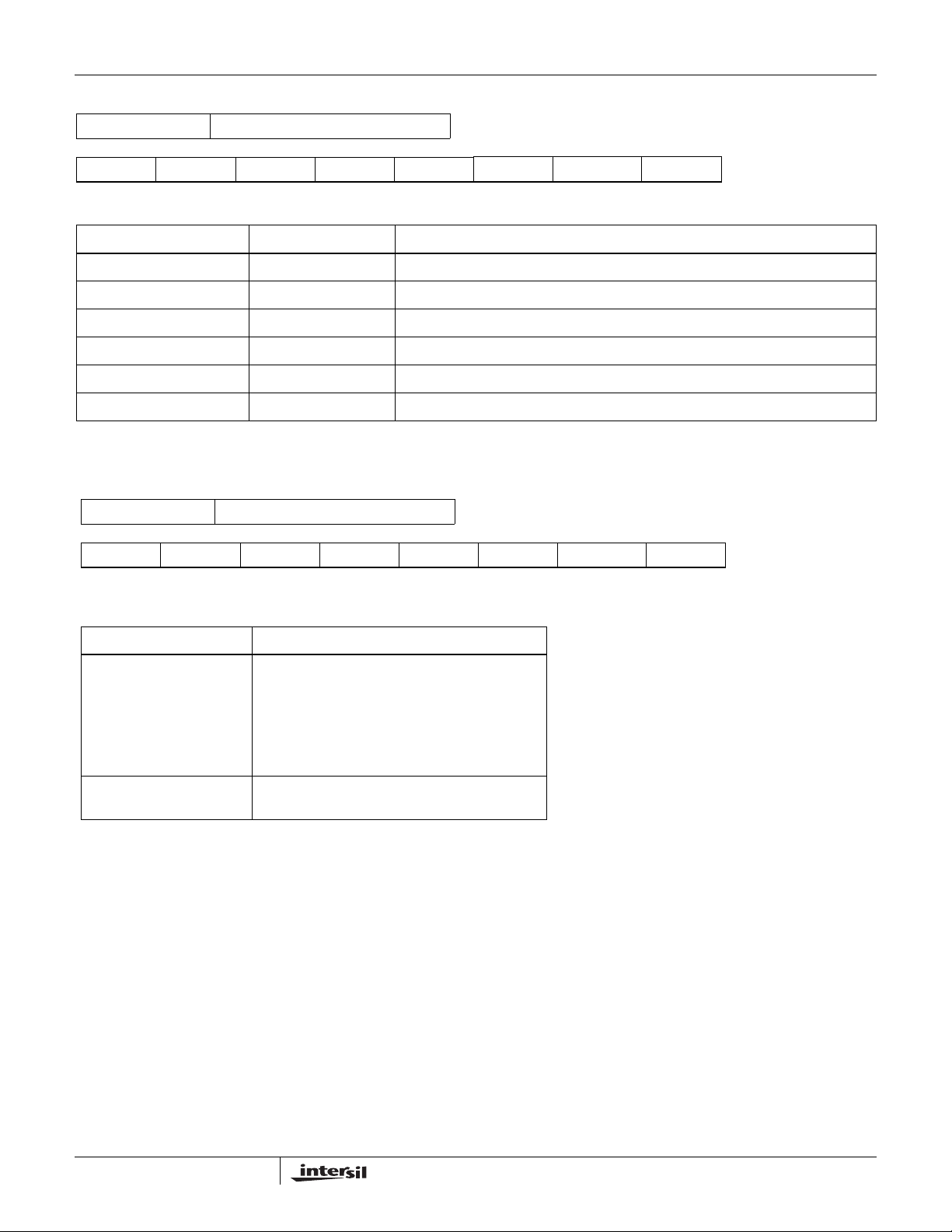
ISL97635A
REGISTER 0x02 FAULT/STATUS REGISTER
RESERVED RESERVED 2_CH_SD 1_CH_SD BL_STAT OV_CURR THRM_SHDN FAULT
Bit 7 (R) Bit 6 (R) Bit 5 (R) Bit 4 (R) Bit 3 (R) Bit 2 (R) Bit 1 (R) Bit 0 (R)
BIT BIT ASSIGNMENT BIT FIELD DEFINITIONS
Bit 5 2_CH_SD = Two LED output channels are shutdown (1 = shutdown, 0 = OK)
Bit 4 1_CH_SD = One LED output channel is shutdown (1 = shutdown, 0 = OK)
Bit 3 BL_STAT = BL Status (1 = BL On, 0 = BL Off)
Bit 2 OV_CURR = Input Overcurrent (1 = Overcurrent condition, 0 = Current OK)
Bit 1 THRM_SHDN = Thermal Shutdown (1 = Thermal Fault, 0 = Thermal OK)
Bit 0 FAULT = Fault occurred (Logic “OR” of all of the fault conditions)
FIGURE 25. DESCRIPTIONS OF FAULT/STATUS REGISTER
REGISTER 0x03 ID REGISTER
LED PANEL MFG3 MFG2 MFG1 MFG0 REV2 REV1 REV0
Bit 7 = 1 Bit 6 (R) Bit 5 (R) Bit 4 (R) Bit 3 (R) Bit 2 (R) Bit 1 (R) Bit 0 (R)
BIT ASSIGNMENT BIT FIELD DEFINITIONS
MFG[3..0]
REV[2..0] = Silicon rev (Rev 0 through Rev 7 allowed for
= Manufacturer ID. See “Identification Register
(0x03)” on page 21.
data 0 to 8 in decimal correspond to other vendors
data 9 in decimal represents Intersil ID
data 10 to 14 in decimal are reserved
data 15 in decimal Manufacturer ID is not
implemented
silicon spins)
FIGURE 26. DESCRIPTIONS OF ID REGISTER
22
FN6564.2
December 22, 2008
Page 23

ISL97635A
REGISTER 0x07 DC BRIGHTNESS CONTROL REGISTER
BRTDC7 BRTDC6 BRTDC5 BRTDC4 BRTDC3 BRTDC2 BRTDC1 BRTDC0
Bit 7 (R/W) Bit 6 (R/W) Bit 5 (R/W) Bit 4 (R/W) Bit 3 (R/W) Bit 2 (R/W) Bit 1 (R/W) Bit 0 (R/W)
BIT ASSIGNMENT BIT FIELD DEFINITIONS
BRTDC[7..0]
= 256 steps of DC brightness levels
FIGURE 27. DESCRIPTIONS OF DC BRIGHTNESS CONTROL REGISTER
DC Brightness Control Register (0x07)
The DC Brightness Control Register 0x07 allows users to
have additional dimming flexibility as:
1. Achieving effectively 16 -b it of dimming control when
combined DC dimming with PWM dimming or
2. Achieving visual or audio noise free 8-bit DC dimming
over potentially noisy PWM dimming.
The bit assignment is shown in Figure 27. All of the bits in
this Register can be read or write. Steps 0 to 255 represent
the linear steps of current adjustment in DC on the fly. It can
also be considered as the peak current factory calibration
feature to account for various LED production batches
variations but external EEPROM settings storing and
restoring are required.
• An SMBus Write Byte cycle to register 0x07 sets the
brightness level in DC only.
• An SMBus Read Byte cycle to register 0x07 returns the
current DC brightness level.
• Default value for register 0x07 is 0xFF.
users to set the boost conversion switching frequency
between 1.2MHz and 600kHz.
The bit assignment is shown in Figure 28. Default value for
register 0x08 is 0xFF
Output Channel Mask/Fault Readout Register
(0x09)
This register can be read or write; the bit position
corresponds to the channel. For example, bit 0 corresponds
to Ch0 and bit 5 corresponds to Ch5 and so on. When
writing data to this register, it enables the channels of
interest. When reading data from this register, any disabled
channel and any faulted out channel will read as 0. This
allows the user to determine which channel is faulty and
optionally not enabling it to allow the rest of the system to
continue to function. Additionally, a faulted out channel can
be disabled and re-enabled in order to allow a retry for any
faulty channel without having to power-down the other
channels.
The bit assignment is shown in Figure 29. Default for register
0x09 is 0xFF.
Configuration Register (0x08)
The Configuration Register allows users to set 2 levels of
channel Short-Circuit thresholds or disable it. It also allows
REGISTER 0x08 CONFIGURATION REGISTER
RESERVED RESERVED RESERVED RESERVED RESERVED FSW VSC1 VSC0
Bit 7 (R/W) Bit 6 (R/W) Bit 5 (R/W) Bit 4 (R/W) Bit 3 (R/W) Bit 2 (R/W) Bit 1 (R/W) Bit 0 (R/W)
BIT ASSIGNMENT BIT FIELD DEFINITIONS
VSC[1..0]
FSW[2] 2 levels of Switching Frequencies (1 = 1,200kHz, 0 = 600kHz)
2 levels of Short-Circuit Thresholds (1 = 8V , 0 = 3.1V, accuracy ±15%)
FIGURE 28. DESCRIPTIONS OF CONFIGURATION REGISTER
23
FN6564.2
December 22, 2008
Page 24

ISL97635A
REGISTER 0x09 OUTPUT CHANNEL REGISTER
RESERVED RESERVED CH5 CH4 CH3 CH2 CH1 CH0
Bit 7 (R/W) Bit 6 (R/W) Bit 5 (R/W) Bit 4 (R/W) Bit 3 (R/W) Bit 2 (R/W) Bit 1 (R/W) Bit 0 (R/W)
BIT ASSIGNMENT BIT FIELD DEFINITIONS
CH[5..0] CH5 = Channel 5, CH4 = Channel 4 and so on
FIGURE 29. OUTPUT CHANNEL REGISTER
Components Selections
According to the inductor Voltage-Second Balance principle,
the change of inductor current during the switching regulator
On-time is equal to the change of inductor current during the
switching regulator Off-time. Since the voltage across an
inductor is:
VLL Δ ILΔt⁄×=
and ΔI
@ On = ΔIL @ Off, therefore:
L
0) L⁄ DtS× VOVDVI––()=× L1( D) tS×–×⁄–
V(
I
where D is the switching duty cycle defined by the turn-on
time over the switching period. V
is Schottky diode forward
D
voltage that can be neglected for approximation.
Rearranging the terms without accounting for V
boost ratio and duty cycle respectively as Equations 18
and 19:
OVI
11D–()⁄=⁄
( VI) VO⁄–=
O
V
DV
Input Capacitor
Switching regulators require input capacitors to deliver peak
charging current and to reduce the impedance of the input
supply. This reduces interaction between the regulator and
input supply, improving system stability. The high switching
frequency of the loop causes almost all ripple current to flow
in the input capacitor, which must be rated accordingly.
A capacitor with low internal series resistance should be
chosen to minimize heating effects and improve system
efficiency, such as X5R or X7R ceramic capacitors, which
offer small size and a lower value of temperature and voltage
coefficient compared to other ceramic capacitors.
In boost mode, input current flows continuously into the
inductor, with an AC ripple component proportional to the
rate of inductor charging only and smaller value input
capacitors may be used. It is recommended that an input
capacitor of at least 10µF be used. Ensure the voltage rating
(EQ. 16)
(EQ. 17)
gives the
D
(EQ. 18)
(EQ. 19)
of the input capacitor is suitable to handle the full supply
range.
Inductor
The selection of the inductor should be based on its
maximum current (I
) characteristics, power dissipation
SAT
(DCR), EMI susceptibility (shielded vs unshielded), and size.
Inductor type and value influence many key parameters,
including ripple current, current limit, efficiency, transient
performance and stability.
Its maximum current capability must be adequate to handle
the peak current at the worst case condition. If an inductor
core is chosen with too low a current rating, saturation in the
core will cause the effective inductor value to fall, leading to
an increase in peak to average current level, poor efficiency
and overheating in the core. The series resistance, DCR,
within the inductor causes conduction loss and heat
dissipation. A shielded inductor is usually more suitable for
EMI susceptible applications, such as LED backlighting.
The peak current can be derived from the fact that the
voltage across the inductor during the Off-period can be
shown as Equation 20:
IL
peak
VO( IO) 85%( VI) 12VIVO( VI) L( VOfS)××⁄–×[]⁄+×⁄×=
(EQ. 20)
The choice of 85% is just an average term for the efficiency
approximation. The first term is average current that is
inversely proportional to the input voltage. The second term
is inductor current change that is inversely proportional to L
and f
. As a result, for a given switching frequency and
S
minimum input voltage the system operates, the inductor
I
must be chosen carefully. At a given inductor size,
SAT
usually the larger the inductance, the higher the series
resistance because of the extra winding of the coil. Thus, the
higher the inductance, the lower the peak current capability.
The ISL97635A current limit may also have to be taken into
account.
Output Capacitors
The output capacitor acts to smooth the output voltage and
supplies load current directly during the conduction phase of
the power switch. Output ripple voltage consists of the
discharge of the output capacitor for I
during FET On
LPEAK
24
FN6564.2
December 22, 2008
Page 25
ISL97635A
and the voltage drop due to flowing through the ESR of the
output capacitor. The ripple voltage can be shown as
Equation 21:
ΔV
COI(OCO
DfS) I(OESR×()+⁄×⁄=
(EQ. 21)
The conservation of charge principle in Equation 19 also
brings up a fact that during the boost switch off-period, the
output capacitor is charged with the inductor ripple current
minus a relatively small output current in boost topology. As
a result, the users need to select an output capacitor with
low ESD and with a enough input ripple current capability.
Output Ripple
ΔVCo can be reduced by increasing CO or fS, or using small
ESR capacitors. In general, ceramic capacitors are the best
choice for output capacitors in small to medium sized LCD
backlight applications due to their cost, form factor, and low
ESR.
A larger output capacitor will also ease the driver respond
during PWM dimming Off-period due to the longer sample
and hold effect of the output drooping. The driver does not
need to boost harder in the next On-period that minimizes
transient current. The output capacitor is also needed for
compensation and in general 2x4.7µF/50V ceramic
capacitors are suitable for the notebook display backlight
applications.
Schottky Diode
A high speed rectifier diode is necessary to prevent
excessive voltage overshoot, especially in the boost
configuration. Low forward voltage and reverse leakage
current will minimize losses, making Schottky diodes the
preferred choice. Although the Schottky diode turns on only
during the boost switch Off-period, it carries the same peak
current as the inductor’s, and therefore, a suitable current
rated Schottky diode must be used.
Applications
High Current Applications
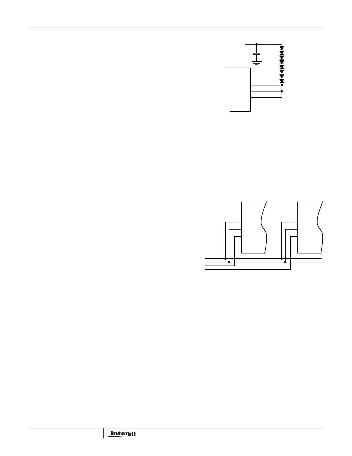
Each channel of the ISL97635A can support up to 35mA.
For applications that need higher current, multiple channels
can be grouped to achieve the desirable current. For
example, the cathode of the last LED can be connected to
IIN0 to IIN2; this configuration can be treated as a single
string with 105mA current driving capability.
.
IIN0
IIN1
IIN2
FIGURE 30. GROUPING MULTIPLE CHANNELS FOR HIGH
CURRENT APPLICATIONS
V
OUT
Multiple Drivers Operation
For large LCD panels where more than 6 channels of LEDs
are needed, multiple ISL97635As with each driver having its
own supporting components can be controlled together with
the common SMBus. While the ISL97635A does not have
extra pins strappable slave address feature, a separate EN
signal can be applied to each driver for asynchronous
operation. A trade-off of such scheme is that an exact faulty
channel cannot be identified if the EN/PWMI signal is
common to all drivers.
SMBCLK
SMBDAT
EN1
EN2
SMBCLK
SMBDAT
EN/PWMI
FIGURE 31. MULTIPLE DRIVERS OPERATION
SMBCLK
SMBDAT
EN/PWMI
16-Bit Dimming
The SMBus controlled PWM and DC dimmings can be
combined to effectively provide 16 bits of dimming capability ,
which can be valuable for automotive and avionics display
applications. Figure 32 illustrates one programming example
where 256 steps of PWM dimming can be programmed
between each DC dimming steps or vice versa.
25
FN6564.2
December 22, 2008
Page 26

ISL97635A
STEP 255 PWM CONTROL
STEP 0~255 DC CONTROL
STEP 254 PWM CONTROL
STEP 1 PWM CONTROL
STEPS 0~255 DC
STEP 0 PWM CONTROL
FIGURE 32. 16-BIT DIMMING ILLUSTRATION
RGB LED Backlight or Scrolling Backlight
Operation
The SMBus control features of PWM dimming, DC dimming,
and random channels selection have offered many driving
possibilities. For example, red, green, and blue LEDs can be
arranged in Ch0 and Ch1, Ch2 and Ch3, Ch4 and Ch5
respectively such that each group can be controlled
independently in sequential order for RGB LED backlighting
applications.
Compensation
The ISL97635A has two main elements in the system; the
Current Mode Boost Regulator and the op amp based
multi-channel current sources. The ISL97635A incorporates
a transconductance amplifier in its feedback path to allow
the user some levels of adjustment on the transient
response and better regulation. The ISL97635A uses current
mode control architecture, which has a fast current sense
loop and a slow voltage feedback loop. The fast current
feedback loop does not require any compensation. The slow
voltage loop must be compensated for stable operation. The
compensation network is a series Rc, Cc1 network from
COMP pin to ground and an optional Cc2 capacitor
connected to the COMP pin. The Rc sets the high frequency
integrator gain for fast transient response and the Cc1 sets
the integrator zero to ensure loop stability. For most
applications, Rc is in the range of 200Ω to 3kΩ and Cc1 is in
the range of 27nF to 37nF. Depending upon the PCB layout,
a Cc2, in range of 100nF , may be needed to create a pole to
cancel the output capacitor ESR’s zero effect for stability.
The ISL97635A evaluation board is configured with Rc1 of
500Ω, Cc1 of 33nF, and Cc2 of 0, which achieves stability. In
the actual applications, these values may need to be tuned
empirically but the recommended values are usually a good
starting point.
All Intersil U.S. products are manufactured, assembled and tested utilizing ISO9000 quality systems.
Intersil Corporation’s quality certifications can be viewed at www.intersil.com/design/quality
Intersil products are sold by description only. Intersil Corporation reserves the right to make changes in circuit design, software and/or specifications at any time without
notice. Accordingly, the reader is cautioned to verify that data sheets are current before placing orders. Information furnished by Intersil is believed to be accurate and
reliable. However, no responsibility is assumed by Intersil or its subsidiaries for its use; nor for any infringements of patents or other rights of third parties which may result
from its use. No license is granted by implicat ion or oth erwise u nde r any p a tent or p at ent r ights of Intersil or its subsidiaries.
For information regarding Intersil Corporation and its products, see www.intersil.com
26
FN6564.2
December 22, 2008
Page 27
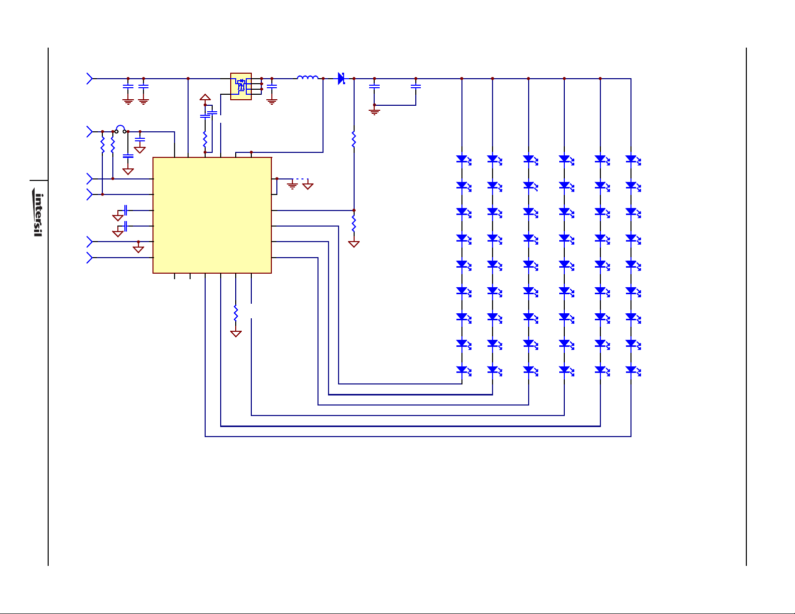
27
VIN
VLOGIC
SMBCLK
SMBDAT
GND
PWMI/EN
10µ/25V
R6
10k
27n/6.3V
220n/6.3V
C1
JP26
R5
10k
C13
C11
1µ/10V
C14
C2
0.1µ/25V
C12
0.1µ/10V
1
SMBCLK
2
SMBDAT
3
FPWM
4
PWMO
5
GND
PWMI/EN
6
U1
24
VDC
NC
7NC8
C10
33n
R7
500
22
23
VIN
ISL97635A
4
3
FDMA530PZ
C20
21
COMP
FAULT
IIN59IIN4
10
Q1
1
2
5
6
19
20
LX
LX
PGND
PGND
OVP
IIN0
IIN1
IIN2
IIN3
RSET
11
12
L1 : IHLP-2525BD-01 Vishay Inductor,
L1
8.2µH
C4
10µ/25V
18
17
16
15
14
13
OVP
D1
D1 : SS15 - Vishay Schottky Diode, 5
SS15
R3
1M
R4
39k
C6
4.7µ/50V
C7
4.7µ/50V
LED1
LED2
LED3
LED4
LED5
LED6
LED10
LED11
LED12
LED13
LED14
LED15
LED19
LED20
LED21
LED22
LED23
LED24
LED28
LED29
LED30
LED31
LED32
LED33
LED37
LED38
LED39
LED40
LED41
LED42
LED46
LED47
LED48
LED49
LED50
ISL97635A
LED51
R2
36.6k
NOTES:
FOR 2 LAYERS BOARD, LAYOUT
PGND (NOISY GROUND) ON TOP
LAYER AND AGND (QUIET GROUND)
ON BOTTOM LAYER. TIE PGND AND
December 22, 2008
AGND ONLY AT ONE POINT BY DOING
THIS: BRIDGE U1 PGND (PINS 18 AND 19)
AND AGND (PIN 5) TO THE PACKAGE
THERMAL PAD. PUT MULTIPLE VIAS ON THE
THERMAL PAD THAT CONNECTS TO THE
FN6564.2
BOTTOM SIDE AGND.
LED7
LED8
LED9
LED16
LED17
LED18
LED25
LED26
LED27
LED34
LED35
LED36
LED43
LED44
LED45
LED52
LED53
LED54
FIGURE 33. TYPICAL APPLICATION CIRCUIT
Page 28
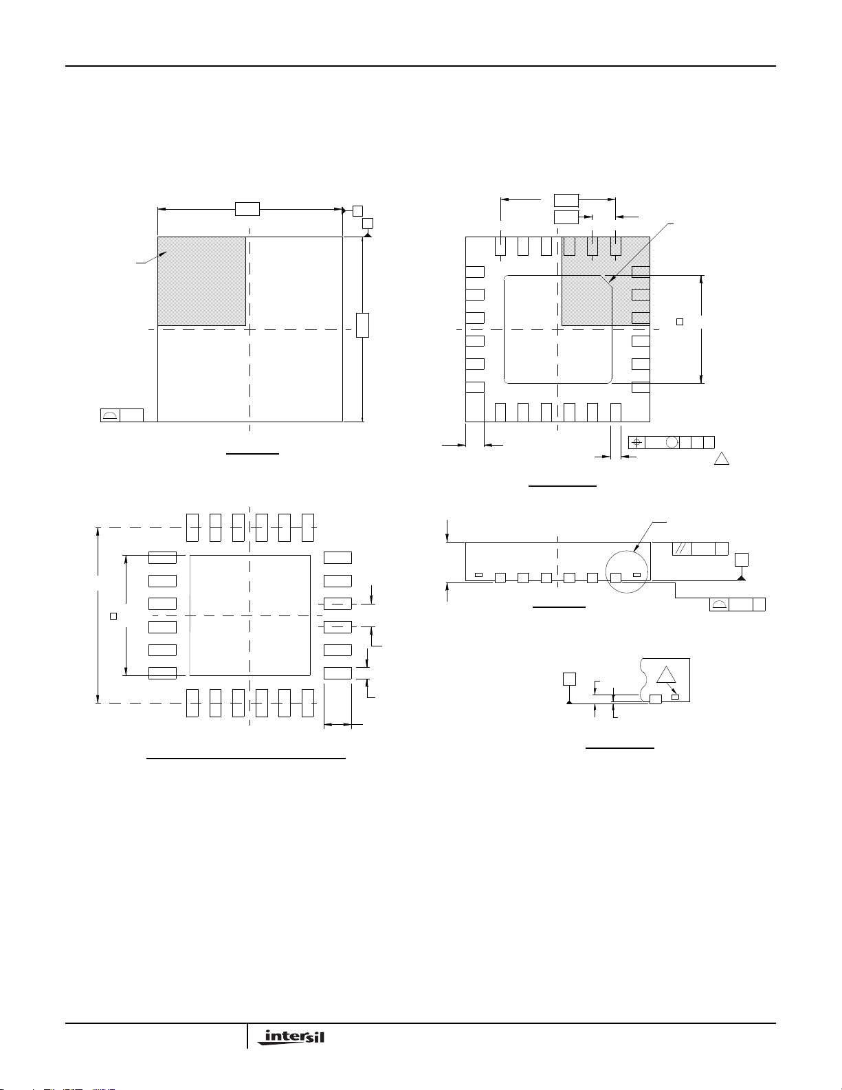
Package Outline Drawing
L24.4x4D
24 LEAD QUAD FLAT NO-LEAD PLASTIC PACKAGE
Rev 2, 10/06
4.00
ISL97635A
A
B
4X
2.5
20X
19
0.50
24
PIN #1 CORNER
(C 0 . 25)
INDEX AREA
(4X)
( 3 . 8 TYP )
( 2 . 50 )
PIN 1
0.15
TOP VIEW
4.00
0 . 90 ± 0 . 1
( 20X 0 . 5 )
712
1
0.10 M C A B
24X 0 . 23
SEE DETAIL "X"
2 . 50 ± 0 . 15
+ 0 . 07
4
- 0 . 05
C
0.10
C
18
13
24X 0 . 4 ± 0 . 1
BOTTOM VIEW
BASE PLANE
SIDE VIEW
SEATING PLANE
0.08 C
TYPICAL RECOMMENDED LAND PATTERN
28
( 24X 0 . 25 )
( 24X 0 . 6 )
0 . 2 REF
C
0 . 00 MIN.
0 . 05 MAX.
5
DETAIL "X"
NOTES:
Dimensions are in millimeters.1.
Dimensions in ( ) for Reference Only.
Dimensioning and tolerancing conform to AMSE Y14.5m-1994.
2.
3.
Unless otherwise specified, tolerance : Decimal ± 0.05
4.
Dimension b applies to the metallized terminal and is measured
between 0.15mm and 0.30mm from the terminal tip.
Tiebar shown (if present) is a non-functional feature.
5.
The configuration of the pin #1 identifier is optional, but must be
6.
located within the zone indicated. The pin #1 identifier may be
either a mold or mark feature.
FN6564.2
December 22, 2008
 Loading...