

Page 1
®
www.BDTIC.com/Intersil
ISL97516
Data Sheet May 9, 2008
600kHz/1.2MHz PWM Step-Up Regulator
The ISL97516 is a high frequency, high efficiency step-up
voltage regulator operated at constant frequency PWM
mode. With an internal 2.0A, 200mΩ MOSFET, it can deliver
up to 1A output current at over 90% efficiency. The
selectable 600kHz and 1.2MHz allows smaller inductors and
faster transient response. An external compensation pin
gives the user greater flexibility in setting frequency
compensation allowing the use of low ESR Ceramic output
capacitors.
When shut down, it draws <1µA of current and can operate
down to 2.3V input supply. These features along with
1.2MHz switching frequency makes it an ideal device for
portable equipment and TFT-LCD displays.
The ISL97516 is available in an 8 Ld MSOP package with a
maximum height of 1.1mm. The device is specified for
operation over the full -40°C to +85°C temperature range.
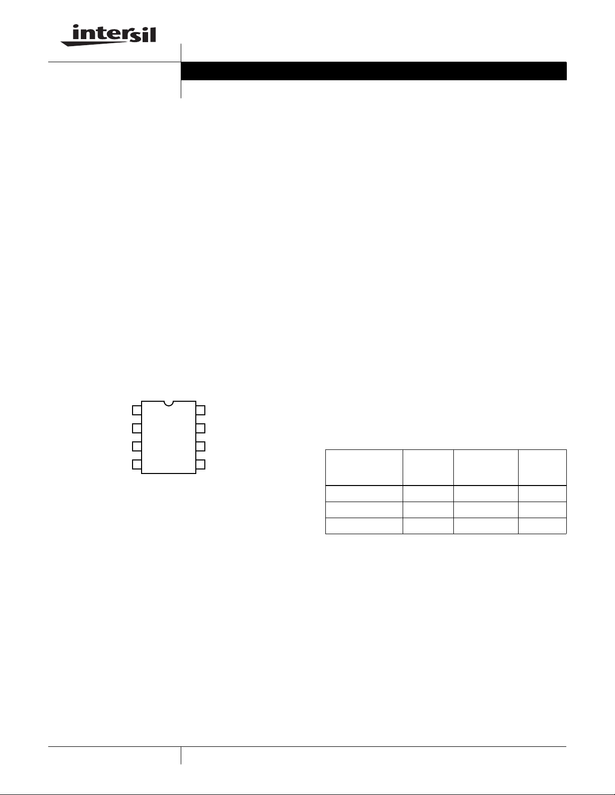
Pinout
ISL97516
(8 LD MSOP)
TOP VIEW
COMP SS
1
FB FSEL
2
EN VDD
3
GND LX
4
8
7
6
5
FN9261.3
Features
• >90% Efficiency
• 2.0A, 200mΩ Power MOSFET
• 2.3V to 5.5V Input
• Up to 25V Output
• 600kHz/1.2MHz Switching Frequency Selection
• Adjustable Soft-Start
• Internal Thermal Protection
• 1.1mm Max Height 8 Ld MSOP Package
• Pb-free Available (RoHS compliant)
Applications
• TFT-LCD displays
• DSL modems
• PCMCIA cards
• Digital cameras
• GSM/CDMA phones
• Portable equipment
• Handheld devices
Ordering Information
PART
NUMBER
(Note)
ISL97516IUZ 7516Z 8 Ld MSOP MDP0043
ISL97516IUZ-T* 7516Z 8 Ld MSOP MDP0043
ISL97516IUZ-TK* 7516Z 8 Ld MSOP MDP0043
*Please refer to TB347 for details on reel specifications.
NOTE: Intersil Pb-free plus anneal products employ special Pb-free
material sets; molding compounds/die attach materials and 100%
matte tin plus anneal plate termination finish, which are RoHS
compliant and compatible with both SnPb and Pb-free soldering
operations. Intersil Pb-free products are MSL classified at Pb-free
peak reflow temperatures that meet or exceed the Pb-free
requirements of IPC/JEDEC J STD-020.
PART
MARKING
PACKAGE
(Pb-free)
PKG.
DWG. #
1
CAUTION: These devices are sensitive to electrostatic discharge; follow proper IC Handling Procedures.
1-888-INTERSIL or 1-888-468-3774
| Intersil (and design) is a registered trademark of Intersil Americas Inc.
Copyright Intersil Americas Inc. 2006, 2007, 2008. All Rights Reserved
All other trademarks mentioned are the property of their respective owners.
Page 2
ISL97516
www.BDTIC.com/Intersil
Absolute Maximum Ratings (T
LX to GND . . . . . . . . . . . . . . . . . . . . . . . . . . . . . . . . . . . . . . . . . .27V
V
to GND. . . . . . . . . . . . . . . . . . . . . . . . . . . . . . . . . . . . . . . . 6.5V
DD
COMP, FB, EN, SS, FSEL to GND . . . . . . . . . -0.3V to (V
CAUTION: Do not operate at or near the maximum ratings listed for extended periods of time. Exposure to such conditions may adversely impact product reliability and
result in failures not covered by warranty.
IMPORTANT NOTE: All parameters having Min/Max specifications are guaranteed. Typical values are for information purposes only. Unless otherwise noted, all tests
are at the specified temperature and are pulsed tests, therefore: TJ = TC = T
Electrical Specifications V
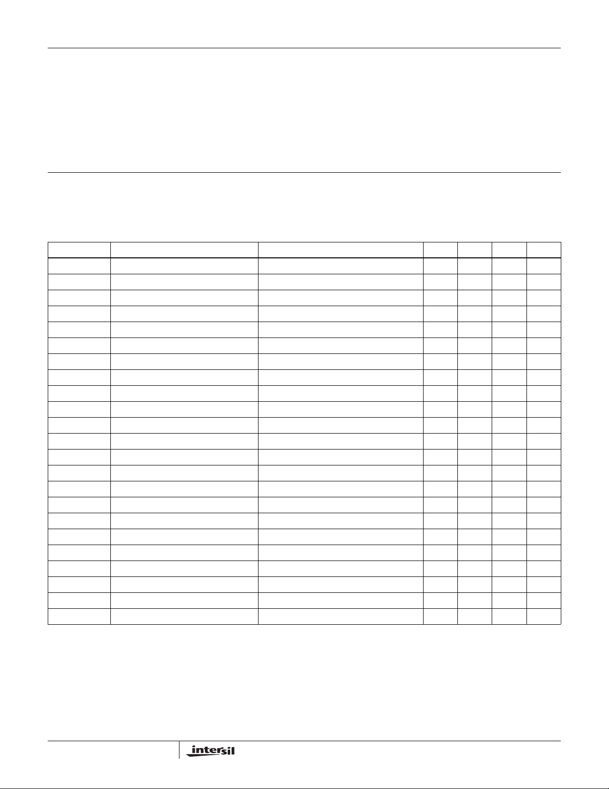
PARAMETER DESCRIPTION CONDITIONS MIN TYP MAX UNIT
IQ1 Quiescent Current - Shutdown EN = 0V 1 5 µA
IQ2 Quiescent Current - Not Switching EN = V
IQ3 Quiescent Current - Switching EN = V
V
FB
I
B-FB
V
DD
- 600kHz Maximum Duty Cycle FSEL = 0V 85 92 %
D
MAX
- 1.2MHz Maximum Duty Cycle FSEL = V
D
MAX
I
LIM
I
EN
r
DS(ON)
I
LX-LEAK
/ΔVINLine Regulation 3V < VIN < 5.5V, V
ΔV
OUT
/ΔI
ΔV
OUT
f
OSC1
f
OSC2
V
IL
V
IH
G
M
V
DD-ON
HYS V
I
SS
OTP Over-Temperature Protection 150 °C
Feedback Voltage 1.272 1.294 1.309 V
Feedback Input Bias Current 0.01 0.5 µA
Input Voltage Range 2.3 5.5 V
Current Limit - Max Peak Input Current 1.5 2.0 A
Shutdown Input Bias Current EN = 0V 0.01 0.5 µA
Switch ON-Resistance VDD = 2.7V, ILX = 1A 0.2 Ω
Switch Leakage Current VSW = 27V 0.01 3 µA
Load Regulation VIN = 3.3V , V
OUT
Switching Frequency Accuracy FSEL = 0V 500 620 740 kHz
Switching Frequency Accuracy FSEL = V
EN, FSEL Input Low Level 0.5 V
EN, FSEL Input High Level 1.5 V
Error Amp Tranconductance ΔI = 5µA 70 130 150 1µ/Ω
VDD UVLO On Threshold 2.1 2.2 2.3 V
UVLO Hysteresis 100 mV
DD
Soft-Start Charge Current 4 6 8 µA
= +25°C) Thermal Information
A
Storage Temperature. . . . . . . . . . . . . . . . . . . . . . . .-65°C to +150°C
Operating Ambient Temperature . . . . . . . . . . . . . . . .-40°C to +85°C
+0.3V)
DD
A
= 3.3V, V
IN
limits are 100% tested at +25°C, unless otherwise specified. Temperature limits est ablished by characterization
and are not production tested.
OUT
= 12V, I
= 0mA, FSEL = GND, TA = -40°C to +85°C; Parameters with MIN and/or MAX
OUT
DD
DD
Operating Junction Temperature . . . . . . . . . . . . . . . . . . . . . . +135°C
Power Dissipation . . . . . . . . . . . . . . . . . . . . . . . . . . . . . See Curves
Pb-free reflow profile . . . . . . . . . . . . . . . . . . . . . . . . . .see link below
http://www.intersil.com/pbfree/Pb-FreeReflow.asp
, FB = 1.3V 0.7 mA
, FB = 1.0V 3 4 mA
DD
= 12V 0.2 %
OUT
= 12V , IO = 30mA to 200mA 0.3 %
OUT
DD
85 90 %
1000 1250 1500 kHz
2
FN9261.3
May 9, 2008
Page 3
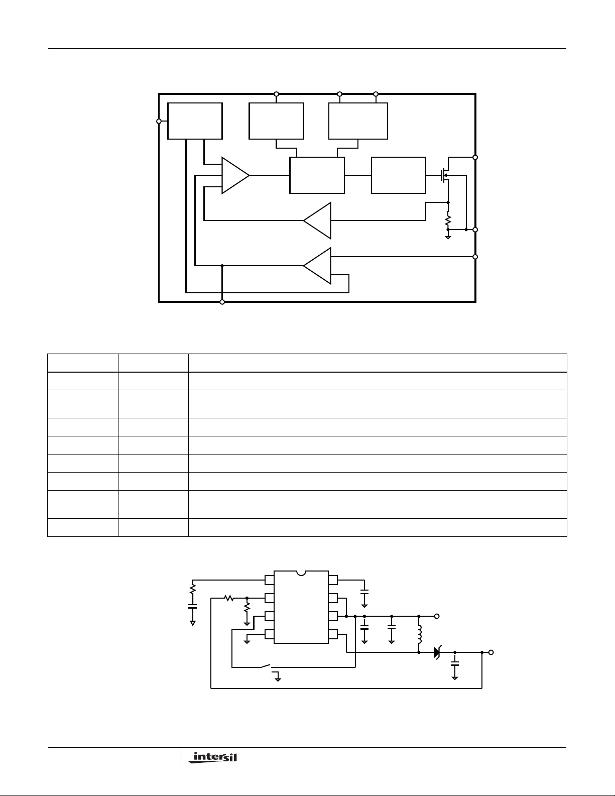
Block Diagram
www.BDTIC.com/Intersil
ISL97516
EN SS
SHUTDOWN
AND START -UP
CONTROL
VDD
REFERENCE
GENERATOR
COMPARATOR
COMP
FSEL
OSCILLATOR
CURRENT
SENSE
GM
AMPLIFIER
PWM LOGIC
CONTROLLER
Pin Descriptions
PIN NUMBER PIN NAME DESCRIPTION
FET
DRIVER
LX
GND
FB
1 COMP Compensation pin. Output of the internal error amplifier. Capacitor and resistor from COMP pin to ground.
2 FB Voltage feedback pin. Internal reference is 1.294V nominal. Connect a resistor divider from V
V
3 EN Shutdown control pin. Pull EN low to turn off the device.
4 GND Analog and power ground.
5 LX Power switch pin. Connected to the drain of the internal power MOSFET.
6 VDD Analog power supply input pin.
7 FSEL Frequency select pin. When FSEL is set low, switching frequency is set to 620kHz. When connected to
high or V
8 SS Soft-start control pin. Connect a capacitor to control the converter start-up.
Typical Application Circuit
R
3
3.9kΩ
C
5
4.7nF
= 1.294V (1 + R1/R2). See “Typical Application Circuit” on page 3.
OUT
, switching frequency is set to 1.25MHz.
DD
SS
FSEL
VDD
LX
8
7
6
5
C
3
27nF
C
4
0.1µF
+
C
1
22µF
1
85.2kΩR
R
10kΩ
1
COMP
FB
2
2
S1
EN
3
GND
4
10µH
D
1
2.3V TO 5.5V
C
+
2
22µF
12V
OUT
.
3
FN9261.3
May 9, 2008
Page 4
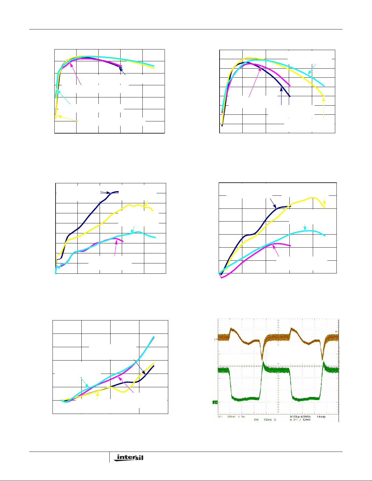
Typical Performance Curves
www.BDTIC.com/Intersil
95
90
85
80
VIN = 5V, VO = 12V, fs = 620kHz
75
EFFICIENCY (%)
VIN = 5V, VO = 9V, fs = 620kHz
70
65
60
0 200 400 600 800 1000
FIGURE 1. BOOST EFFICIENCY vs I
VIN = 5V, VO = 12V, fs = 1.25MHz
VIN = 5V, VO = 9V, fs = 1.25MHz
I
(mA)
OUT
OUT
ISL97516
92
90
88
86
84
82
VIN = 3.3V, VO = 12V,
f
80
EFFICIENCY (%)
78
76
74
= 620kHz
s
0 100 200 300 400 500
VIN = 3.3V, VO = 12V,
f
I
OUT
VIN = 3.3V, VO = 9V,
f
s
= 1.25MHz
s
VIN = 3.3V, VO = 9V,
= 1.25MHz
f
s
(mA)
= 620kHz
FIGURE 2. BOOST EFFICIENCY vs I
OUT
0.9
VIN = 5V, VO = 12V,
0.8
= 1.25MHz
f
s
0.7
0.6
0.5
0.4
0.3
LOAD REGULATION (%)
0.2
0.1
0
0 200 400 600 800 1000
VIN = 5V, VO = 12V,
= 620kHz
f
s
I
OUT
VIN = 5V, VO = 9V,
fs = 1.25MHz
VIN = 5V, VO = 9V,
= 620kHz
f
s
(mA)
FIGURE 3. LOAD REGULATION vs I
0.6
0.5
0.4
0.3
VO = 12V, IO = 80mA
= 1.25MHz
f
0.2
s
VO = 9V, IO = 100mA
= 620kHz
f
s
OUT
0.7
VIN = 3.3V, VO = 12V,
f
= 1.25MHz
s
0
0 100 200 300 400 500
LOAD REGULATION (%)
0.6
0.5
0.4
0.3
0.2
0.1
VIN = 3.3V, VO = 9V,
= 1.25MHz
f
s
VIN = 3.3, VO = 9V,
fs = 1.25kHz
VIN = 3.3, VO = 12V,
= 620kHz
f
s
I
(mA)
OUT
FIGURE 4. LOAD REGULATION vs I
= 50mA TO 300mA
I
O
VIN = 3.3V
VO = 12V
f
= 600kHz
s
OUT
0.1
LINE REGULATION (%)
VO = 9V, IO = 80mA
(V)
= 1.25MHz
f
s
IN
FIGURE 6. TRANSIENT RESPONSE
-0.1
0
2
VO = 12V, IO = 80mA
= 620kHz
f
s
3 4 5 6
V
FIGURE 5. LINE REGULATION vs V
IN
4
FN9261.3
May 9, 2008
Page 5
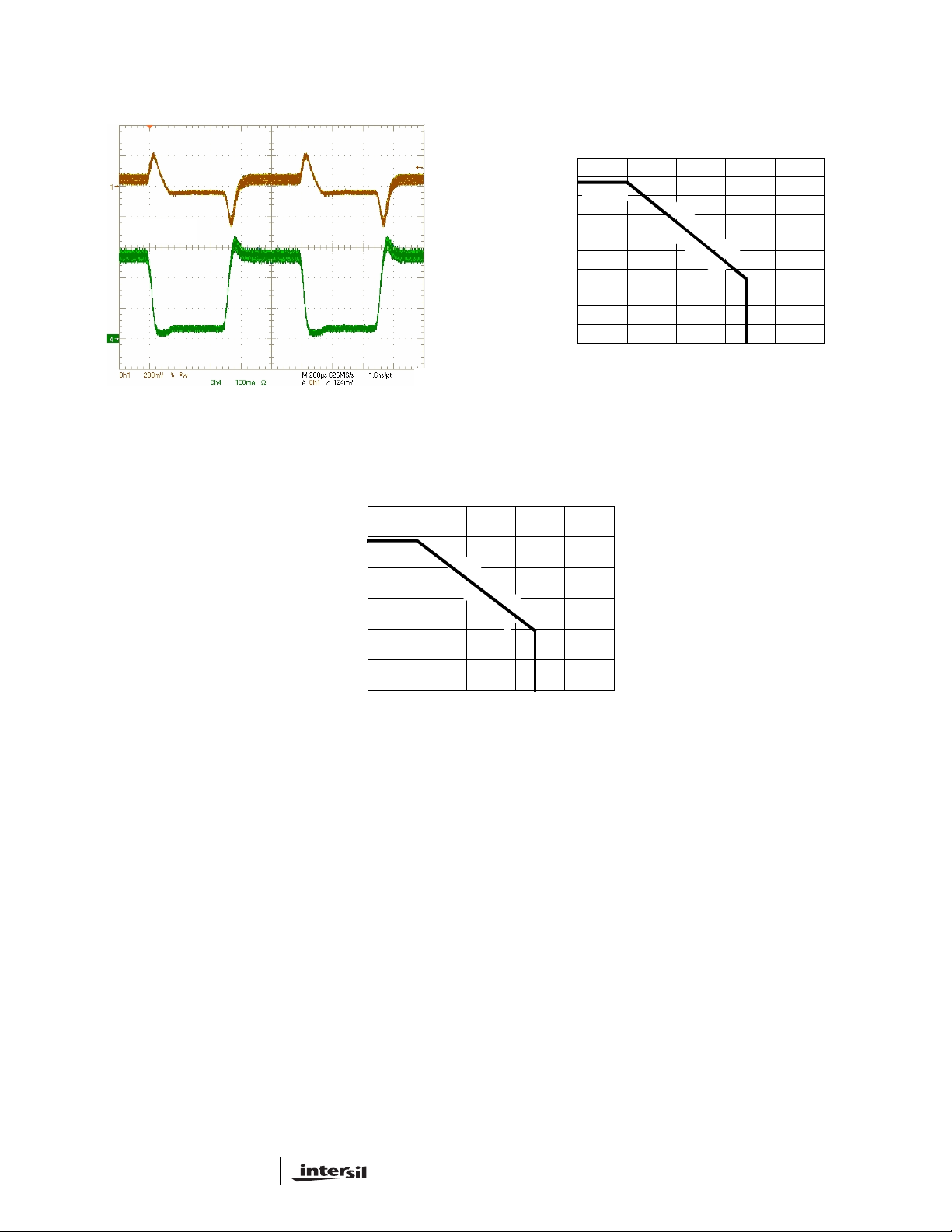
Typical Performance Curves (Continued)
www.BDTIC.com/Intersil
ISL97516
JEDEC JESD51-7 HIGH EFFECTIVE THERMAL
CONDUCTIVITY TEST BOARD
1.0
0.9
870mW
0.8
0.7
0.6
0.5
0.4
0.3
0.2
POWER DISSIPATION (W)
0.1
0
0 25 50 75 100 125
AMBIENT TEMPERATURE (°C)
M
θ
S
J
O
A
=
P
8
+
1
1
5
°
C
/
W
85
VIN = 3.3V
VO = 12V
f
s
= 1.2MHz
= 50mA TO 300mA
I
O
FIGURE 7. TRANSIENT RESPONSE FIGURE 8. PACKAGE POWER DISSIPA TION vs AMBIENT
TEMPERATURE
JEDEC JESD51-3 LOW EFFECTIVE THERMAL
CONDUCTIVITY TEST BOARD
0.6
0.5
486mW
0.4
0.3
0.2
M
θ
S
J
O
A
=
P
+
8
2
0
6
°
C
/
W
0.1
POWER DISSIPATION (W)
0.0
0 255075100125
AMBIENT TEMPERATURE (°C)
FIGURE 9. PACKAGE POWER DISSIPATION vs AMBIENT TEMPERATURE
Applications Information
The ISL97516 is a high frequency, high efficiency boost
regulator operated at constant frequency PWM mode. The
boost converter stores energy from an input voltage source
and deliver it to a higher output voltage. The input voltage
range is 2.3V to 5.5V and output voltage range is 5V to 25V.
The switching frequency is selectable between 600kHz and
1.2MHz allowing smaller inductors and faster transient
response. An external compensation pin gives the user
greater flexibility in setting output transient response and
tighter load regulation. The converter soft-start characteristic
can also be controlled by external C
allows the user to completely shutdown the device.
Boost Converter Operations
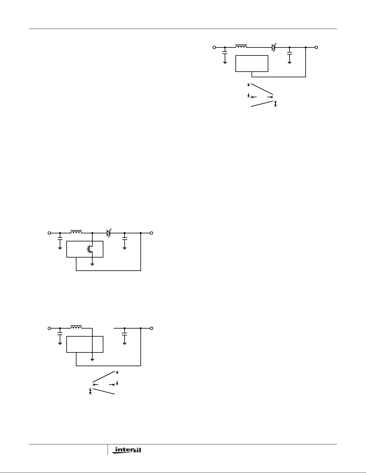
Figure 10 shows a boost converter with all the key
components. In steady state operating and continuous
conduction mode where the inductor current is continuous,
capacitor. The EN pin
SS
85
the boost converter operates in two cycles. During the first
cycle, as shown in Figure 11, the internal power FET turns
on and the Schottky diode is reverse biased and cuts off the
current flow to the output. The output current is supplied
from the output capacitor. The volt age across the inductor is
V
and the inductor current ramps up in a rate of VIN/L, L is
IN
the inductance. The inductance is magnetized and energy is
stored in the inductor. The change in inductor current is
shown in Equation 1:
V
IN
Δt1
D
----------
f
SW
I
----------------
C
×=
OUT
OUT
---------
L
Δt
×=
1
(EQ. 1)
ΔI
Δt1
D Duty Cycle=
ΔV
L1
=
O
5
FN9261.3
May 9, 2008
Page 6
ISL97516
www.BDTIC.com/Intersil
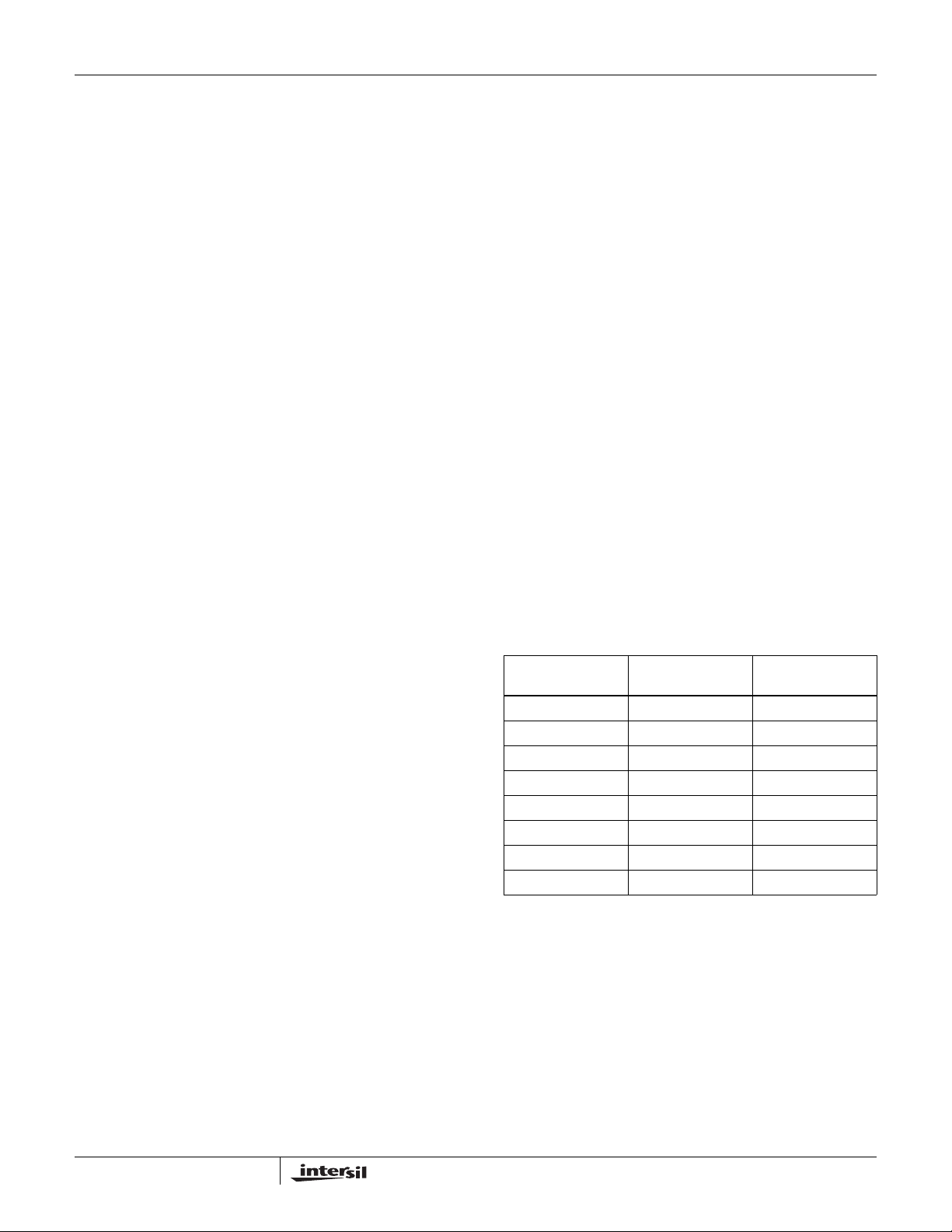
During the second cycle, the power FET turns off and the
Schottky diode is forward biased, (Figure 12). The energy
stored in the inductor is pumped to the output supplying
output current and charging the output capacitor. The
Schottky diode side of the inductor is clamp to a Schottky
diode above the output voltage. So the voltage drop across
the inductor is V
IN
- V
. The change in inductor current
OUT
during the second cycle is:
V
–
INVOUT
=
1D–
-------------
f
SW
×=
------------------------------- -
L
(EQ. 2)
ΔILΔt2
Δt2
For stable operation, the same amount of energy stored in
the inductor must be taken out. The change in inductor
current during the two cycles must be the same.
ΔI1 ΔI2+ 0=
D
----------
f
SW
V
OUT
--------------- -
V
IN
V
1D–
IN
---------
-------------
L
f
SW
1
-------------
=
1D–
V
IN
C
IN
FIGURE 10. BOOST CONVERTER
–
V
INVOUT
------------------------------- -
×+× 0=
L
LD
ISL97516
(EQ. 3)
V
OUT
C
OUT
LD
V
IN
ΔV
C
OUT
O
C
IN
ISL97516
I
ΔT
L
2
ΔI
L2
V
OUT
FIGURE 12. BOOST CONVERTER - CYCLE 2, POWER
SWITCH OPEN
Output Voltage
An external feedback resistor divider is required to divide the
output voltage down to the nominal 1.294V reference
voltage. The current drawn by the resistor network should be
limited to maintain the overall converter efficiency. The
maximum value of the resistor network is limited by the
feedback input bias current and the potential for noise being
coupled into the feedback pin. A resistor network less than
100k is recommended. The boost converter output voltage is
determined by the relationship in Equation 4:
R
⎛⎞
1
V
OUTVFB
-------
1
+
×=
⎜⎟
R
⎝⎠
2
(EQ. 4)
The nominal VFB voltage is 1.294V.
Inductor Selection
The inductor selection determines the output ripple voltage,
transient response, output current capability, and efficiency.
Its selection depends on the input voltage, output voltage,
switching frequency, and maximum output current. For most
applications, the inductance should be in the range of 2µH to
33µH. The inductor maximum DC current specification must
be greater than the peak inductor current required by the
regulator. The peak inductor current can be calculated using
Equation 5:
L
V
IN
C
IN
ISL97516
C
OUT
V
OUT
I
L PEAK()
Output Capacitor
I
OUTVOUT
------------------------------------
Low ESR capacitors should be used to minimized the output
voltage ripple. Multilayer ceramic capacitors (X5R and X7R) are
I
ΔV
L
O
ΔI
L1
Δt
1
FIGURE 11. BOOST CONVERTER - CYCLE 1, POWER
SWITCH CLOSED
preferred for the output capacitors because of their lower ESR
and small packages. T ant alum capacitors with higher ESR can
also be used. The output ripple can be calculated in Equation 6:
I
OUT
-------------------------
ΔV
O
f
×
SWCO
For noise sensitive applications, a 0.1µF placed in parallel
with the larger output capacitor is recommended to reduce
the switching noise coupled from the LX switching node.
6
×
V
IN
V
INVOUTVIN
-----------------------------------------------------
×+=
12⁄
LV
OUT
–()×
FREQ××
(EQ. 5)
D×
I
OUT
ESR×+=
(EQ. 6)
FN9261.3
May 9, 2008
Page 7
ISL97516
www.BDTIC.com/Intersil
Schottky Diode
In selecting the Schottky diode, the reverse break down
voltage, forward current and forward voltage drop must be
considered for optimum converter performance. The diode
must be rated to handle 2.0A, the current limit of the
ISL97516. The breakdown voltage must exceed the
maximum output voltage. Low forward voltage drop, low
leakage current, and fast reverse recovery will help the
converter to achieve the maximum efficiency.
Input Capacitor
The value of the input capacitor depends upon the input and
output voltages, the maximum output current, the inductor
value and the noise allowed to put back on the input line. For
most applications, a minimum 10µF is required. For
applications that run close to the maximum output current
limit, input capacitor in the range of 22µF to 47µF is
recommended.
The ISL97516 is powered from the VIN. A High frequency
0.1µF bypass cap is recommended to be close to the VIN
pin to reduce supply line noise and ensure stable operation.
Loop Compensation
The ISL97516 incorporates a transconductance amplifier in
its feedback path to allow the user some adjustment on the
transient response and better regulation. The ISL97516
uses current mode control architecture, which has a fast
current sense loop and a slow voltage feedback loop. The
fast current feedback loop does not require any
compensation. The slow voltage loop must be compensated
for stable operation. The compensation network is a series
RC network from COMP pin to ground. The resistor sets the
high frequency integrator gain for fast transient response
and the capacitor sets the integrator zero to ensure loop
stability. For most applications, the compensation resistor in
the range of 2k to 7.5k and the compensation capacitor in
the range of 3nF to 10nF.
Soft-Start
The soft-start is provided by an internal 6µA current source
which charges the external C
; the peak MOSFET current
SS
is limited by the voltage on the capacitor. This in turn controls
the rising rate of the output voltage. The regulator goes
through the start-up sequence as well after the EN pin is
pulled to HI.
Frequency Selection
The ISL97516 switching frequency can be user selected to
operate at either constant 620kH z or 1. 25 MH z. Connecting
FSEL pin to ground sets the PWM switching frequency to
620kHz. When connecting FSEL high or VDD, the switching
frequency is set to 1.25MHz.
Maximum Output Current
The MOSFET current limit is nominally 2.0A and guaranteed
1.7A. This restricts the maximum output current, I
OMAX
,
based on Equation 7:
ILI
L-AVG
12⁄ΔIL×()+=
(EQ. 7)
where:
I
= MOSFET current limit
L
I
= average inductor current
L-AVG
ΔIL = inductor ripple current
V
INVOVDIODE
------------------------------------------------------------------------------
ΔI
=
L
LV
V
= Schottky diode forward voltage, typically, 0.6V
DIODE
+()VIN–[]×
( V
O
DIODE
) fS×+×
(EQ. 8)
fS = switching frequency, 600kHz or 1.2MHz
I
OUT
-------------
L-AVG
=
1D–
(EQ. 9)
I
D = MOSFET turn-on ratio:
D1
Table 1 gives typical maximum I
V
+
OUTVDIODE
values for 1.2MHz
OUT
(EQ. 10)
V
IN
--------------------------------------------
–=
switching frequency and 10µH inductor.
TABLE 1.
V
IN
(V)
2.5 5 870
2.5 9 500
2.5 12 380
3.3 5 1150
3.3 9 655
3.3 12 500
5 9 990
5 12 750
V
OUT
(V)
I
OMAX
(mA)
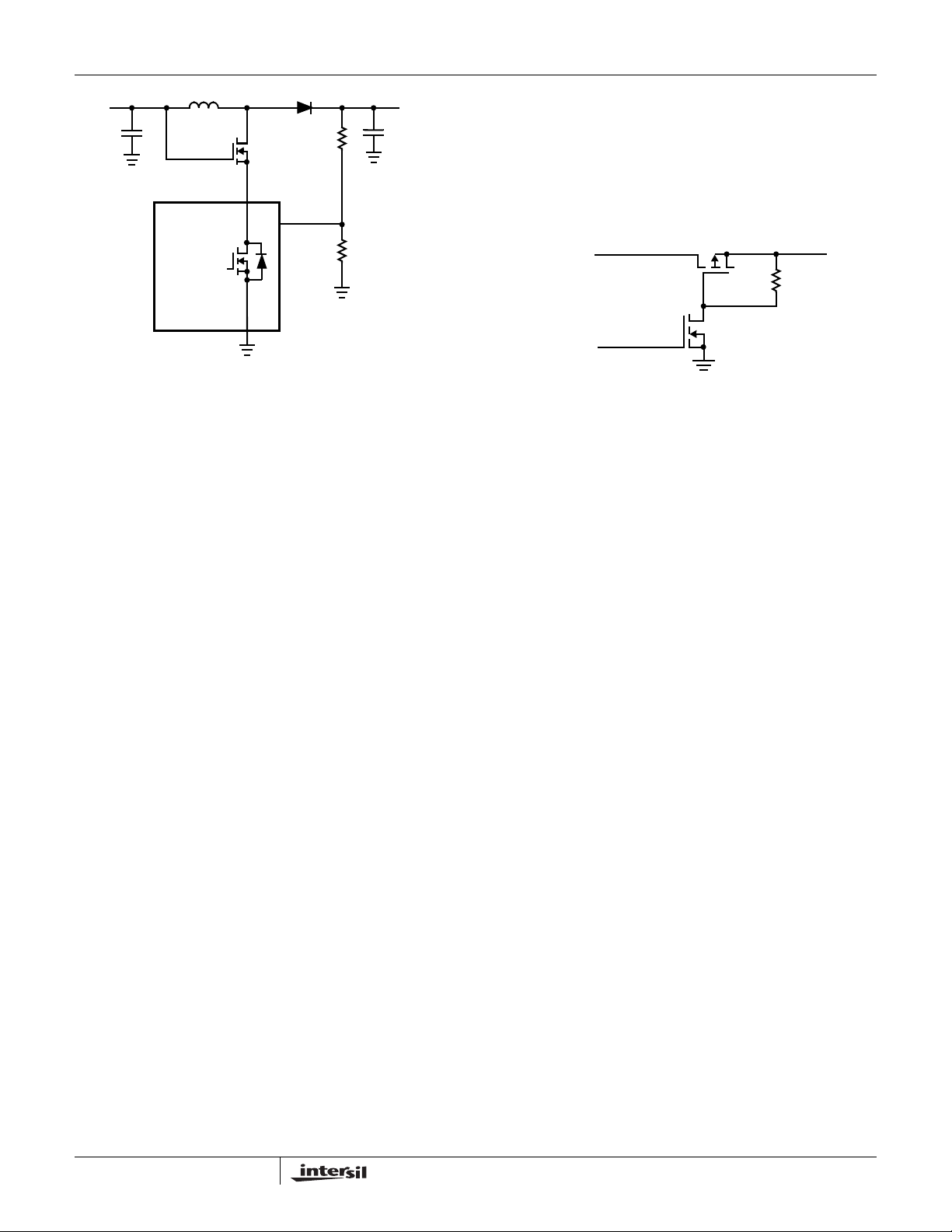
Cascaded MOSFET Application
An 25V N-Channel MOSFET is integrated in the boost
regulator. For the applications where the output voltage is
greater than 25V, an external cascaded MOSFET is needed
as shown in Figure 12. The voltage rating of the external
MOSFET should be greater than A
VDD
.
Shutdown Control
When the EN pin is pulled down, the ISL97516 is shutdown
reducing the supply current to <1µA.
7
FN9261.3
May 9, 2008
Page 8
ISL97516
www.BDTIC.com/Intersil
V
IN
LX
INTERSIL
ISL97516
FIGURE 13. CASCADED MOSFET TOPOLOGY FOR HIGH
OUTPUT VOLTAGE APPLICATIONS
FB
A
VDD
DC PATH BLOCK APPLICATION
Note that there is a DC path in the boost converter from the
input to the output through the inductor and diode, hence the
input voltage will be seen at output with a forward voltage
drop of diode before the part is enabled. If this voltage is not
desired, the following circuit can be inserted between input
and inductor to disconnect the DC path when the part is
disabled.
TO INDUCTOR
EN
FIGURE 14. CIRCUIT TO DISCONNECT THE DC PA TH OF
BOOST CONVERTER
INPUT
8
FN9261.3
May 9, 2008
Page 9
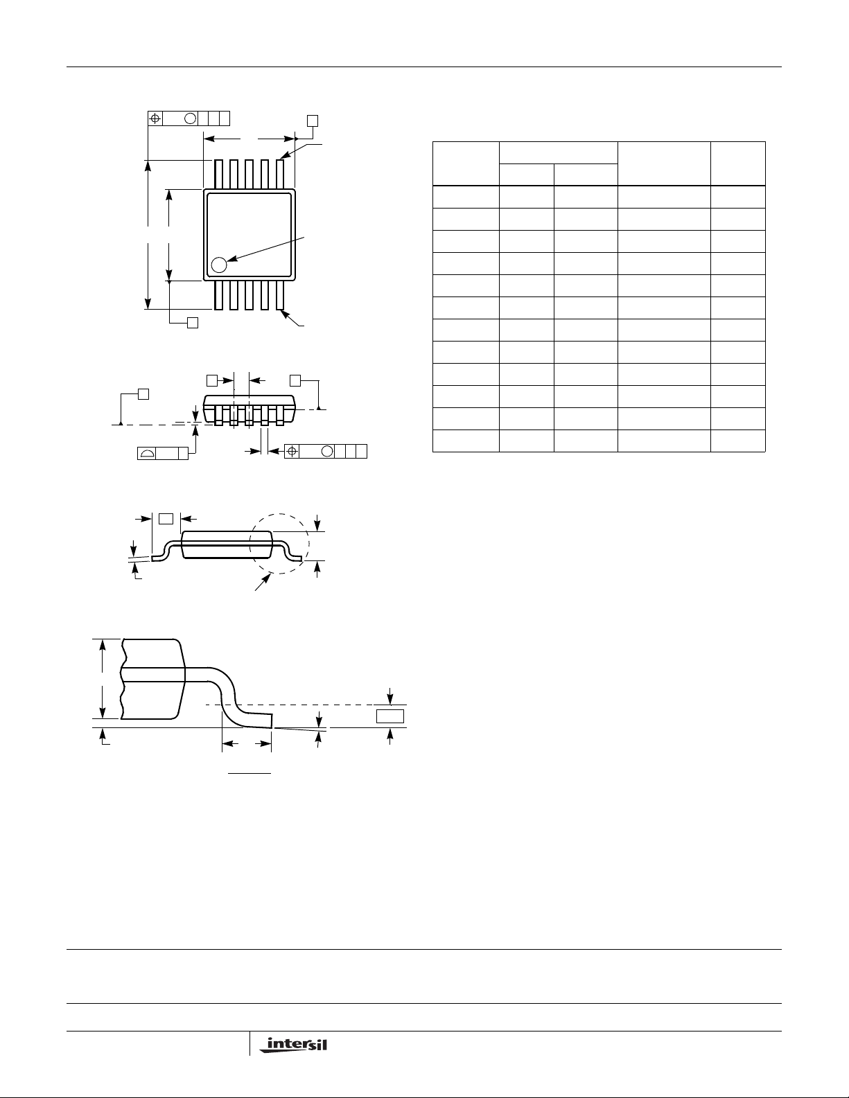
Mini SO Package Family (MSOP)
www.BDTIC.com/Intersil
M
C
SEATING
PLANE
0.10 C
N LEADS
c
0.25 C A B
E1E
B
e
L1
SEE DETAIL "X"
D
N
1
b
A
(N/2)+1
PIN #1
I.D.
(N/2)
H
M
0.08 C A B
A
ISL97516
MDP0043
MINI SO PACKAGE FAMILY
SYMBOL
NOTES:
1. Plastic or metal protrusions of 0.15mm maximum per side are not
2. Plastic interlead protrusions of 0.25mm maximum per side are
3. Dimensions “D” and “E1” are measured at Datum Plane “H”.
4. Dimensioning and tolerancing per ASME Y14.5M-1994.
MILLIMETERS
TOLERANCE NOTESMSOP8 MSOP10
A1.101.10 Max. A1 0.10 0.10 ±0.05 A2 0.86 0.86 ±0.09 -
b 0.33 0.23 +0.07/-0.08 -
c0.180.18 ±0.05 D 3.00 3.00 ±0.10 1, 3
E4.904.90 ±0.15 -
E1 3.00 3.00 ±0.10 2, 3
e0.650.50 Basic L0.550.55 ±0.15 -
L1 0.95 0.95 Basic -
N 8 10 Reference -
Rev. D 2/07
included.
not included.
A2
GAUGE
A1
L
DETAIL X
PLANE
3° ±3°
0.25
All Intersil U.S. products are manufactured, assembled and tested utilizing ISO9000 quality systems.
Intersil Corporation’s quality certifications can be viewed at www.intersil.com/design/quality
Intersil products are sold by description only. Intersil Corporation reserves the right to make changes in circuit design, software and/or specifications at any time without
notice. Accordingly, the reader is cautioned to verify that data sheets are current before placing orders. Information furnished by Intersil is believed to be accurate and
reliable. However, no responsibility is assumed by Intersil or its subsidiaries for its use; nor for any infringements of patents or other rights of third parties which may result
from its use. No license is granted by implic atio n or other wise u nde r any p a tent or patent rights of Intersil or its subs idiari es.
For information regarding Intersil Corporation and its products, see www.intersil.com
9
FN9261.3
May 9, 2008
 Loading...