

Page 1
®
www.BDTIC.com/Intersil
ISL90727, ISL90728
Single Volatile 128-Tap XDCP
Data Sheet August 2, 2006
Digitally Controlled Potentiometer
(XDCP™)
The Intersil ISL90727 and ISL90728 are digitally controlled
potentiometers (XDCP). Each device consists of a resistor
array, wiper switches, and a control section. The wiper
position is controlled by an I
2
C interface.
The potentiometer is implemented by a resistor array
composed of 127 resistive elements and a wiper switching
network. Between each element and at either end are tap
points accessible to the wiper terminal. The position of the
wiper element is controlled by the SDA and SCL inputs.
The device can be used in a wide variety of applications
including:
• Mechanical potentiometer replacement
• Transducer adjustment of pressure, temperature, position,
chemical, and optical sensors
• RF amplifier biasing
• LCD brightness and contrast adjustment
• Gain control and offset adjustment
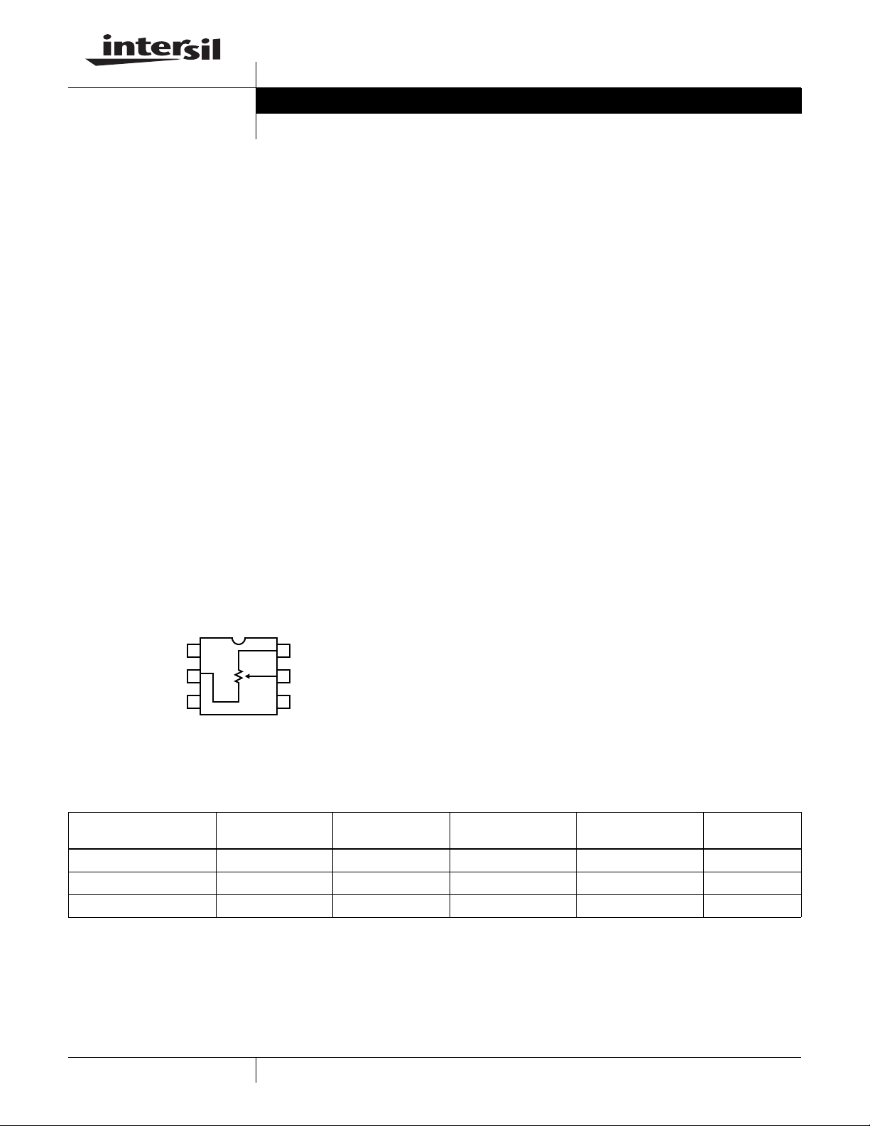
Pinout
ISL90727, ISL90728
(6 LD SC-70)
TOP VIEW
FN8247.4
Features
• Volatile Solid-State Potentiometer
2
•I
C Serial Bus Interface
• DCP Terminal Voltage, 2.7V to 5.5V
•Low Tempco
- Rheostat - 45 ppm/
- Divider - 15 ppm/°C typical
• 128 Wiper Tap Poin ts
- Wiper resistance 70Ω typ at V
• Low Power CMOS
- Active current, 200µA max
- Standby current, 500nA max
• Available R
TOTAL
• Power on Preset to Midscale
• Direct Replacement for AD5247
• Packaging
- 6 Ld SC-70
• Pb-Free Plus Anneal Available (RoHS Compliant)
°C typical
= 3.3V
CC
Values = 50kΩ, 10kΩ
VDD
GND
SCL
1
2
3
6
RH
5
RW
SDA
4
Ordering Information
PART NUMBER
(See Notes 1, 2) PART MARKING R
ISL90727WIE627Z-TK ANH 10 -40 to +85 6 Ld SC-70 P6.049
ISL90727UIE627Z-TK ANI 50 -40 to +85 6 Ld SC-70 P6.049
ISL90728WIE627Z-TK CCF 10 -40 to +85 6 Ld SC-70 P6.049
NOTES:
1. Intersil Pb-free plus anneal products employ special Pb-free material sets; molding compounds/die attach materials and 100% matte tin plate
termination finish, which are RoHS compliant and compatible with both SnPb and Pb-free soldering operations. Intersil Pb-free products are
MSL classified at Pb-free peak reflow temperatures that meet or exceed the Pb-free requirements of IPC/JEDEC J STD-020
2. ISL90727 has an I
2
C address 5Ch and ISL90728 has an I2C address 7Ch
TOTAL
(kΩ)
TEMP RANGE
(°C)
PACKAGE
(Pb-Free) PKG. DWG. #
1
CAUTION: These devices are sensitive to electrostatic discharge; follow proper IC Handling Procedures.
1-888-INTERSIL or 1-888-468-3774
XDCP is a trademark of Intersil Americas Inc. Copyright Intersil Americas Inc. 2005-2006. All Rights Reserved
| Intersil (and design) is a registered trademark of Intersil Americas Inc.
All other trademarks mentioned are the property of their respective owners.
Page 2
ISL90727, ISL90728
www.BDTIC.com/Intersil
Pin Descriptions
PIN NUMBER SYMBOL DESCRIPTION
1 VDD Supply Voltage
2 GND Ground
3 SCL Open drain Serial Clock input
4 SDA Open drain Serial Data I/O
5 RW Potentiometer Wiper Terminal
6 RH Potentiometer High Terminal
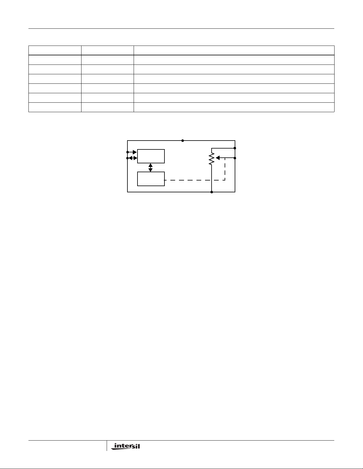
Block Diagram
VDD
SCL
SDA
I2C
INTERFACE
WIPER
REGISTER
RH
RW
RL
GND
2
FN8247.4
August 2, 2006
Page 3
ISL90727, ISL90728
www.BDTIC.com/Intersil
Absolute Maximum Ratings Recommended Operating Conditions
Storage Temperature. . . . . . . . . . . . . . . . . . . . . . . .-65°C to +150°C
Voltage at any Digital Interface Pin
with Respect to V
. . . . . . . . . . . . . . . . . . . . . . . . . . . . . . . . . . . . . . . .-0.3V to +7V
V
CC
Voltage at any DCP Pin with
Respect to V
. . . . . . . . . . . . . . . . . . . . . . -0.3V to VCC+0.3
SS
. . . . . . . . . . . . . . . . . . . . . . . . . . . . -0.3V to V
SS
CC
Lead Temperature (soldering, 10s) . . . . . . . . . . . . . . . . . . . . .300°C
I
(10s) . . . . . . . . . . . . . . . . . . . . . . . . . . . . . . . . . . . . . . . . . . ±6mA
W
Latchup . . . . . . . . . . . . . . . . . . . . . . . . . . . Class II, Level B at 85°C
ESD . . . . . . . . . . . . . . . . . . . . . . . . . . . . . >2kV Human Body Model
CAUTION: Stresses above those listed in “Absolute Maximum Ratings” may cause permanent damage to the device. This is a stress only rating and operation of the
device at these or any other conditions above those indicated in the operational sections of this specification is not implied .
Analog Specifications Over recommended operating conditions unless otherwise stated.
SYMBOL PARAMETER TEST CONDITIONS MIN
R
TOTAL
RH to RL Resistance W option 10 kΩ
U option 50 kΩ
to RL Resistance Tolerance -20 +20 %
R
H
R
W
C
H/CL/CW
I
LkgDCP
Wiper Resistance VCC = 3.3V @ 25°C 85 200 Ω
Potentiometer Capacitance 10/10/
Leakage on DCP Pins
Voltage at pin from GND to V
VOLTAGE DIVIDER MODE
INL Integral Non-linearity -1 ±0.2 1 LSB
DNL Differential Non-linearity Monotonic over all tap positions W option -1 ±0.1 1 LSB
ZSerror
(Note 5)
FSerror
(Note 6)
(Note 12) Ratiometric Temperature Coefficient DCP Register set to 80 hex ±15 ppm/°C
TC
V
Zero-scale Error W option 0 1 3 LSB
U option 0 0.5 1
Full-scale Error W option -3 -1 0 LSB
U option -1 -0.5 0
RESISTOR MODE
RINL
(Note 10)
RDNL
(Note 9)
Integral Non-linearity DCP register set between 20 hex and FF hex.
Monotonic over all tap positions
Differential Non-linearity DCP register set between 20 hex
and FF hex. Monotonic over all tap
positions
Roffset
Offset W option 0 1 3 MI
(Note 8)
U option 0 0.5 1 MI
TC
Resistance Temperature Coefficient DCP register set between 20 hex and FF hex ±45 ppm/°C
R
(Notes 11, 12)
Industrial . . . . . . . . . . . . . . . . . . . . . . . . . . . . . . . . . .-40°C to +85°C
. . . . . . . . . . . . . . . . . . . . . . . . . . . . . . . . . . . . . . . . 2.7V to 5.5V
V
CC
Power Rating of Each DCP . . . . . . . . . . . . . . . . . . . . . . . . . . . .5mW
TYP
(Note 3) MAX UNIT
pF
25
CC
0.1 µA
(Note 4)
(Note 4)
U option -1 ±0.1 1 LSB
(Note 4)
(Note 4)
(Note 4)
-2 ±0.25 2 MI
(Note 7)
W option -1 ±0.1 1 MI
(Note 7)
U option -1 ±0.1 1 MI
(Note 7)
(Note 7)
(Note 7)
3
FN8247.4
August 2, 2006
Page 4
ISL90727, ISL90728
www.BDTIC.com/Intersil
Operating Specifications
TYP
SYMBOL PARAMETER TEST CONDITIONS MIN
I
CC1
I
SB
I
ComLkg
(Note 12) DCP Wiper Response Time SCL falling edge of last bit of DCP Data Byte to
t
DCP
VCC Supply Current
(Volatile write/read)
VCC Current (standby) V
f
= 400kHz; SDA = Open; (for I2C, Active,
SCL
Read and Volatile Write States only)
= +5.5V, I2C Interface in Standby State 500 nA
CC
Common-Mode Leakage Voltage at SDA pin to GND or V
CC
wiper change
Ramp VCC Ramp Rate 0.2 V/ms
V
CC
t
D
Power-up Delay VCC above Vpor, to DCP Initial Value Register
recall completed, and I
2
C Interface in standby state
SERIAL INTERFACE SPECIFICATIONS
V
IL
SDA, and SCL Input Buffer LOW
Voltage
V
IH
SDA, and SCL Input Buffer HIGH
Voltage
Hysteresis SDA and SCL Input Buffer Hysteresis 0.05*
V
OL
Cpin
(Note 14) SDA, and SCL Pin Capacitance 10 pF
f
SCL
t
IN
t
AA
t
BUF
t
LOW
t
HIGH
t
SU:STA
t
HD:STA
t
SU:DAT
t
HD:DAT
t
SU:STO
t
HD:STO
t
DH
(Note 14) SDA and SCL Rise Time From 30% to 70% of V
t
R
SDA Output Buffer LOW Voltage,
Sinking 4mA
SCL Frequency 400 kHz
Pulse Width Suppression Time at
SDA and SCL Inputs
SCL Falling Edge to SDA Output Data
Valid
Time the Bus Must be Free Before the
Start of a New Transmission
Any pulse narrower than the max spec is
suppressed.
SCL falling edge crossing 30% of VCC, until SDA
exits the 30% to 70% of V
window.
CC
SDA crossing 70% of VCC during a STOP
condition, to SDA crossing 70% of V
the following START condition.
CC
during
Clock LOW Time Measured at the 30% of VCC crossing. 1300 ns
Clock HIGH Time Measured at the 70% of VCC crossing. 600 ns
START Condition Setup Time SCL rising edge to SDA falling edge. Both
crossing 70% of V
CC
.
START Condition Hold Time From SDA falling edge crossing 30% of VCC to
SCL falling edge crossing 70% of V
CC
.
Input Data Setup Time From SDA exiting the 30% to 70% of VCC
window, to SCL rising edge crossing 30% of V
CC
Input Data Hold Time From SCL rising edge crossing 70% of VCC to
SDA entering the 30% to 70% of V
window.
CC
STOP Condition Setup Time From SCL rising edge crossing 70% of VCC, to
CC
.
STOP Condition Hold Time for Read,
or Volatile Only Write
SDA rising edge crossing 30% of V
From SDA rising edge to SCL falling edge. Both
crossing 70% of V
CC
.
Output Data Hold Time From SCL falling edge crossing 30% of VCC,
until SDA enters the 30% to 70% of V
CC
window.
CC
0.1 * Cb
(Note 3) MAX UNIT
500 ns
-0.3 0.3*
0.7*
V
CC
V
CC
00.4V
1300 ns
600 ns
600 ns
100 ns
0ns
600 ns
600 ns
0ns
20 +
200 µA
3µA
3ms
V
V
CC
VCC+
V
0.3
V
50 ns
900 ns
250 ns
4
FN8247.4
August 2, 2006
Page 5
ISL90727, ISL90728
www.BDTIC.com/Intersil
Operating Specifications (Continued)
SYMBOL PARAMETER TEST CONDITIONS MIN
t
(Note 14) SDA and SCL Fall Time From 70% to 30% of V
F
(Note 14) Capacitive Loading of SDA or SCL Total on-chip and off-chip 10 400 pF
Cb
(Note 14) SDA and SCL Bus Pull-up Resistor
Rpu
Off-chip
Maximum is determined by tR and tF.
For Cb = 400pF, max is about 2~2.5kΩ.
For Cb = 40pF, max is about 15~20kΩ
CC
20 +
0.1 * Cb
1kΩ
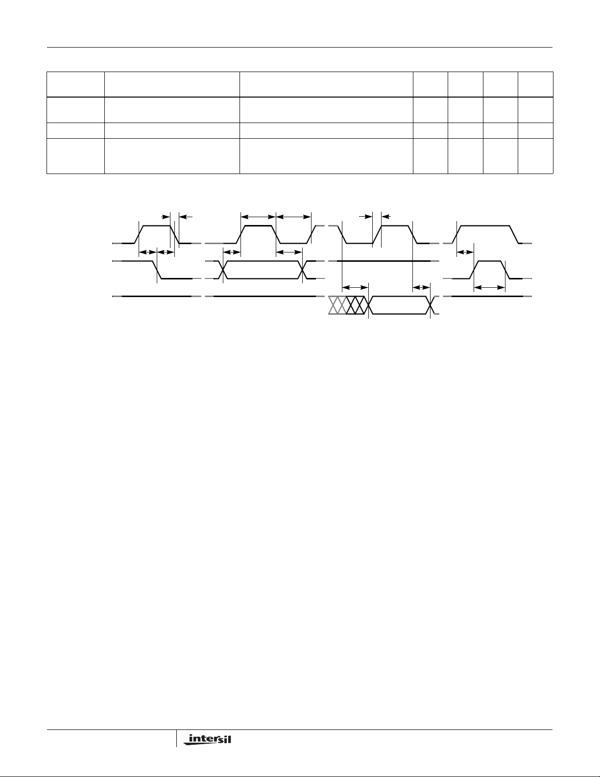
SDA vs SCL Timing
t
F
t
HIGH
t
LOW
t
R
TYP
(Note 3) MAX UNIT
250 ns
---------------- -
×=
125°C
t
SU:DAT
t
BUF
t
SU:STO
t
HD:DAT
t
t
and V(RW)0 are V(RW) for the DCP register set to FF hex and 00 hex respectively . LSB is the
127
and RL.
W
and RH.
W
6
10
minimum value of the resistance over the temperature range.
AA
DH
SCL
t
SU:STA
(INPUT TIMING)
(OUTPUT TIMING)
NOTES:
3. Typical values are for T
4. LSB: [V(R
incremental voltage when changing from one tap to an adjacent tap.
5. ZS error = V(R
6. FS error = [V(R
7. MI =
Roffset = R
8. Roffset = R
9. RDNL = (R
10. RINL = [R
11. for i = 32 to 127, T = -40°C to 85°C. Max( ) is the maximum value of the resistance and Min ( ) is the
TC
12. This parameter is not 100% tested.
13. V
IL
14. These are I2C-specific parameters and are not directly tested. However, they are used in the device testing to validate specifications.
SDA
SDA
– V(RW)0]/127. V(RW)
W)127
/LSB.
W)0
W)127
|R
– R
127
R
= 0V, VIH = V
|/127. R
0
/MI, when measuring between R
0
/MI, when measuring between R
127
– R
)/MI - 1, for i = 32 to 127.
i
i-1
– (MI • i) – R0]/MI, for i = 32 to 127.
i
Max Ri()Min Ri()–[]
--------------------------------------------------------------- -
Max Ri()Min Ri()+[]2⁄
CC.
t
HD:STA
= 25°C and 3.3V supply voltage.
A
– VCC]/LSB.
and R0 are the measured resistances for the DCP register set to FF hex and 00 hex respectively.
127
Principles of Operation
The ISL90727 and ISL90728 are integrated circuits
incorporating one DCP with its associated registers and an
2
I
C serial interface providing direct communication between
a host and the potentiometer.
DCP Description
The DCP is implemented with a combination of resistor
elements and CMOS switches. The physical ends of the DCP
are equivalent to the fixed terminals of a mechanical
potentiometer (R
connected to intermediate nodes, and is equivalent to the wiper
terminal of a mechanical potentiometer. The position of the
wiper terminal within the DCP is controlled by a 7-bit volatile
Wiper Register (WR). The DCP has its own WR. When the WR
of the DCP contains all zeroes (WR<6:0> = 00h), its wiper
and RL pins). The RW pin of the DCP is
H
5
terminal (R
) is closest to its “Low” terminal (RL). When the
W
WR of the DCP contains all ones (WR<6:0> = 7Fh), its wiper
terminal (R
) is closest to its “High” terminal (RH). As the value
W
of the WR increases from all zeroes (00h) to all ones (127
decimal), the wiper moves monotonically from the position
closest to R
to the position closest to RH. At the same time,
L
the resistance between R
while the resistance between R
monotonically. R
the wiper movement will always be relative to R
While the ISL90727 and ISL90728 are being powered up,
the WR is reset to 40h (64 decimal), which locates R
roughly at the center between R
and RL increases monotonically,
W
and RW decreases
is connected to the GND pin of the device, so
L
H
and RH.
L
.
L
W
FN8247.4
August 2, 2006
Page 6

ISL90727, ISL90728
www.BDTIC.com/Intersil
The WR and IVR can be read or written directly using the
2
I
C serial interface as described in the following sections.
I2C Serial Interface
The ISL90727 and ISL90728 support bidirectional bus
oriented protocol. The protocol defines any device that
sends data onto the bus as a transmitter and the receiving
device as the receiver. The device controlling the transfer is
a master and the device being controlled is the slave. The
master always initiates data transfers and provides the clock
for both transmit and receive operations. Therefore, the
ISL90727 and ISL90728 operate as slave devices in all
applications.
All communication over the I
sending the MSB of each byte of data first.
Protocol Conventions
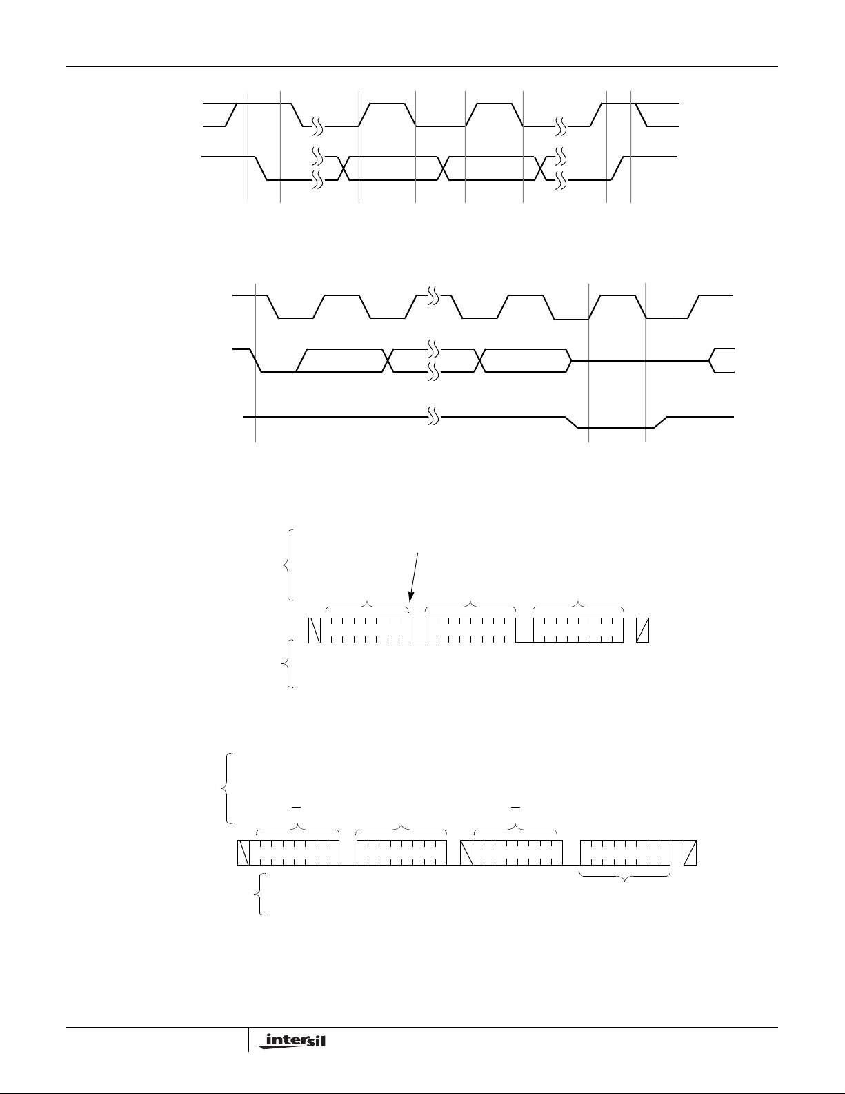
Data states on the SDA line can change only during SCL
LOW periods. SDA state changes during SCL HIGH are
reserved for indicating START and STOP conditions (See
Figure 1). On power-up of the ISL90727 and ISL90728, the
SDA pin is in the input mode.
2
All I
C interface operations must begin with a STAR T condition,
which is a HIGH to LOW transition of SDA while SCL is HIGH.
The ISL90727 and ISL90728 continuously monitor the SDA
and SCL lines for the START condition and do not respond to
any command until this condition is met (See Figure 1). A
ST ART condition is ignored during the power-up sequence and
during internal non-volatile write cycles.
2
All I
C interface operations must be terminated by a STOP
condition, which is a LOW to HIGH transition of SDA while
SCL is HIGH (See Figure 1).
An ACK, Acknowledge, is a software convention used to
indicate a successful data transfer. The transmitting device,
either master or slave, releases the SDA bus after
transmitting eight bits. During the ninth clock cycle, the
receiver pulls the SDA line LOW to acknowledge the
reception of the eight bits of data (See Figure 2).
2
C interface is conducted by
.
ISL90727 0 1 0 1 1 1 0 R/W
ISL90728 0 1 1 1 1 1 0 R/W
TABLE 1. IDENTIFICATION BYTE FORMAT
MSB LSB
Write Operation
A Write operation requires a START condition, followed by a
valid Identification Byte, a valid Address Byte, a Data Byte,
and a STOP condition. After each of the three bytes, the
ISL90727 and ISL90728 respond with an ACK. At this time,
the device enters its standby state (See Figure 3).
Data Protection
A valid Identification Byte, Address Byte, and total number of
SCL pulses act as a protection of both volatile and
non-volatile registers. During a Write sequence, the Data
Byte is loaded into an internal shift register as it is received.
If the Address Byte is 0, the Data Byte is transferred to the
Wiper Register (WR) at the falling edge of the SCL pulse
that loads the last bit (LSB) of the Data Byte. If an address
other than 00h or an invalid slave address is sent, then the
device will respond with no ACK.
Read Operation
A Read operation consist of a three byte instruction followed
by one or more Data Bytes (See Figure 4). The master
initiates the operation issuing the following sequence: a
START, the Identification byte with the R/W
Address Byte, a second START, and a second Identification
byte with the R/W
the ISL90727 and ISL90728 respond with an ACK. Then the
ISL90727 and ISL90728 transmit the Data Byte as long as
the master responds with an ACK during the SCL cycle
following the eighth bit of each byte. The master then
terminates the read operation (issuing a STOP condition)
following the last bit of the Data Byte (See Figure 4).
bit set to “1”. After each of the three bytes,
bit set to “0”, an
The ISL90727 and ISL90728 respond with an ACK after
recognition of a START condition followed by a valid
Identification Byte, and once again after successful receipt of
an Address Byte. The ISL90727 and ISL90728 also respond
with an ACK after receiving a Data Byte of a write operation.
The master must respond with an ACK after receiving a Data
Byte of a read operation.
A valid Identification Byte contains 0101110 as the seven
MSBs for the ISL90727 and 0111110 as the seven MSBs for
the ISL90728. The LSB in the Read/Write
for a Read operation, and “0” for a Write operation (See
Table 1)
6
bit. Its value is “1”
FN8247.4
August 2, 2006
Page 7
SCL
www.BDTIC.com/Intersil
SDA
ISL90727, ISL90728
SCL FROM
MASTER
SDA OUTPUT FROM
TRANSMITTER
SDA OUTPUT FROM
RECEIVER
SIGNALS FROM
START DATA DATA STOP
STABLE CHANGE
DATA
STABLE
FIGURE 1. VALID DATA CHANGES, START AND STOP CONDITIONS
81 9
HIGH IMPEDANCE
START ACK
FIGURE 2. ACKNOWLEDGE RESPONSE FROM RECEIVER
WRITE
S
THE MASTER
T
A
IDENTIFICATION
R
T
BYTE
ADDRESS
BYTE
DATA
BYTE
HIGH IMPEDANCE
S
T
O
P
SIGNAL AT SDA
SIGNALS FROM
THE ISL23711
SIGNALS
FROM THE
MASTER
SIGNAL AT SDA
SIGNALS FROM
THE SLAVE
00011
0000011000000
A
C
K
A
C
K
FIGURE 3. BYTE WRITE SEQUENCE (ISL90727 VERSION SHOWN)
00
S
T
A
IDENTIFICATION
R
T
01011
A
C
K
BYTE WITH
R/W
=1
110
S
T
A
IDENTIFICATION
R
BYTE WITH
T
R/W
00011
ADDRESS
=0
110 0000 00
BYTE
A
C
K
FIGURE 4. READ SEQUENCE (ISL90727 VERSION SHOWN)
A
C
K
A
C
K
DATA BYTE
S
T
O
P
7
FN8247.4
August 2, 2006
Page 8
ISL90727, ISL90728
www.BDTIC.com/Intersil
Small Outline Transistor Plastic Packages (SC70-6)
C
L
A2
A
SEATING
PLANE
0.20 (0.008)
C
L
b
12 3
e1
D
C
L
WITH
PLATING
4X θ1
C
4X θ1
M
e
456
0.10 (0.004) C
c
BASE METAL
L1
C
VIEW C
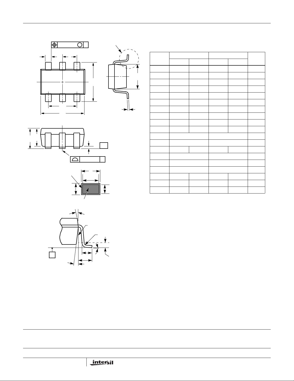
P6.049
6 LEAD SMALL OUTLINE TRANSISTOR PLASTIC PACKAGE
INCHES MILLIMETERS
SYMBOL
NOTESMIN MAX MIN MAX
A 0.031 0.043 0.80 1.10 -
C
L
E
E1
A1 0.000 0.004 0.00 0.10 -
A2 0.031 0.039 0.00 1.00 -
b 0.006 0.012 0.15 0.30 -
b1 0.006 0.010 0.15 0.25
c 0.003 0.009 0.08 0.22 6
C
c1 0.003 0.009 0.08 0.20 6
D 0.073 0.085 1.85 2.15 3
E 0.071 0.094 1.80 2.40 -
E1 0.045 0.053 1.15 1.35 3
A1
SEATING
PLANE
-C-
e 0.0256 Ref 0.65 Ref -
e1 0.0512 Ref 1.30 Ref -
L 0.010 0.018 0.26 0.46 4
L1 0.017 Ref. 0.420 Ref.
L2 0.006 BSC 0.15 BSC
b
b1
N6 65
R 0.004 - 0.10 -
R1 0.004 0.010 0.15 0.25
c1
α
o
0
o
8
o
0
o
8
-
Rev. 2 9/03
NOTES:
1. Dimensioning and tolerance per ASME Y14.5M-1994.
2. Package conforms to EIAJ SC70 and JEDEC MO203AB.
3. Dimensions D and E1 are exclusive of mold flash, protrusions,
R1
R
GAUGE PLANE
L
α
L2
or gate burrs.
4. Footlength L measured at reference to gauge plane.
5. “N” is the number of terminal positions.
6. These Dimensions apply to the flat section of the lead between
0.08mm and 0.15mm from the lead tip.
7. Controlling dimension: MILLIMETER. Converted inch dimensions are for reference only
VIEW C
All Intersil U.S. products are manufactured, assembled and tested utilizing ISO9000 quality systems.
Intersil Corporation’s quality certifications can be viewed at www.intersil.com/design/quality
Intersil products are sold by description only. Intersil Corporation reserves the right to make changes in circuit design, software and/or specifications at any time without
notice. Accordingly, the reader is cautioned to verify that data sheets are current before placing orders. Information furnished by Intersil is believed to be accurate and
reliable. However, no responsibility is assumed by Intersil or its subsidiaries for its use; nor for any infringements of patents or other rights of third parties which may result
from its use. No license is granted by implic atio n or other wise u nde r any p a tent or patent rights of Intersil or its subsidiaries.
For information regarding Intersil Corporation and its products, see www.intersil.com
8
FN8247.4
August 2, 2006
 Loading...