

Page 1
查询ISL90462TIE627-TK供应商
®
ISL90462
Single Volatile 32-tap XDCP
Data Sheet October 7, 2005
Digitally Controlled Potentiometer
(XDCP™)
The Intersil ISL90462 is a digitally controlled potentiometer
(XDCP). Configured as a variable resistor, the device
consists of a resistor array, wiper switches, a control section,
and volatile memory. The wiper position is controlled by a 2pin Up /Down interface.
The potentiometer is implemented by a resistor array
composed of 31 resistive elements and a wiper switching
network. Between each element and at either end are tap
points accessible to the wiper terminal. The position of the
wiper element is controlled by the CS
The device can be used in a wide variety of applications
including:
• LCD contrast control
• Parameter and bias adjustments
• Industrial and Automotive Control
• Transducer adjustment of pressure, temperature, position,
chemical, and optical sensors
• Laser Diode driver biasing
• Gain control and offset adjustment
and U/D inputs.
FN8230.3
Features
• Volatile Solid-State Potentiometer
• 2-pin UP/DN Interface
• DCP Terminal Voltage, 2.7V to 5.5V
• Tempco 35ppm/
°C Typical
• 32 Wiper Tap Points
• Low Power CMOS
- Active current, 25µA max.
- Supply current 0.3µA
• Available R
• Temperature Range
Values = 10kΩ, 50kΩ, 100kΩ
TOTAL
-40°C to +85°C
• Packages
- 6 Ld SC-70, SOT-23
• Pb-Free Plus Anneal Available (RoHS Compliant)
Pinout
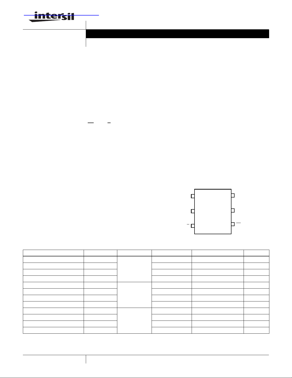
ISL90462
(SOT23, SC70)
TOP VIEW
VDD
RH
GND
U/D
RW
CS
Ordering Information
PART NUMBER PART MARKING R
ISL90462WIE627-TK AJS 10 -40 to +85 6 Ld SC-70 P6.049
ISL90462WIE627Z-TK (See Note) DEK -40 to +85 6 Ld SC-70 (Pb-free) P6.049
ISL90462WIH627-TK AKB -40 to +85 6 Ld SOT-23 P6.064
ISL90462WIH627Z-TK (See Note) DEL -40 to +85 6 Ld SOT-23 (Pb-free) P6.064
ISL90462UIE627-TK AJU 50 -40 to +85 6 Ld SC-70 P6.049
ISL90462UIE627Z-TK (See Note) DEI -40 to +85 6 Ld SC-70 (Pb-free) P6.049
ISL90462UIH627-TK AKD -40 to +85 6 Ld SOT-23 P6.064
ISL90462UIH627Z-TK (See Note) DEJ -40 to +85 6 Ld SOT-23 (Pb-free) P6.064
ISL90462TIE627-TK AJT 100 -40 to +85 6 Ld SC-70 P6.049
ISL90462TIE627Z-TK (See Note) DEG -40 to +85 6 Ld SC-70 (Pb-free) P6.049
ISL90462TIH627-TK AKC -40 to +85 6 Ld SOT-23 P6.064
ISL90462TIH627Z-TK See Note) DEH -40 to +85 6 Ld SOT-23 (Pb-free) P6.064
NOTE: Intersil Pb-free plus anneal products employ special Pb-free material sets; molding compounds/die attach materials and 100% matte tin plate termination finish, which are
RoHS compliant and compatible with both SnPb and Pb-free soldering operations. Intersil Pb-free products are MSL classified at Pb-free peak reflow temperatures that meet or exceed
the Pb-free requirements of IPC/JEDEC J STD-020
(K) TEMP RANGE (°C) PACKAGE (Tape and Reel) PKG. DWG. #
TOTAL
1
CAUTION: These devices are sensitive to electrostatic discharge; follow proper IC Handling Procedures.
1-888-INTERSIL or 1-888-468-3774
XDCP is a trademark of Intersil Americas Inc. Copyright Intersil Americas Inc. 2005. All Rights Reserved
| Intersil (and design) is a registered trademark of Intersil Americas Inc.
All other trademarks mentioned are the property of their respective owners.
Page 2
ISL90462
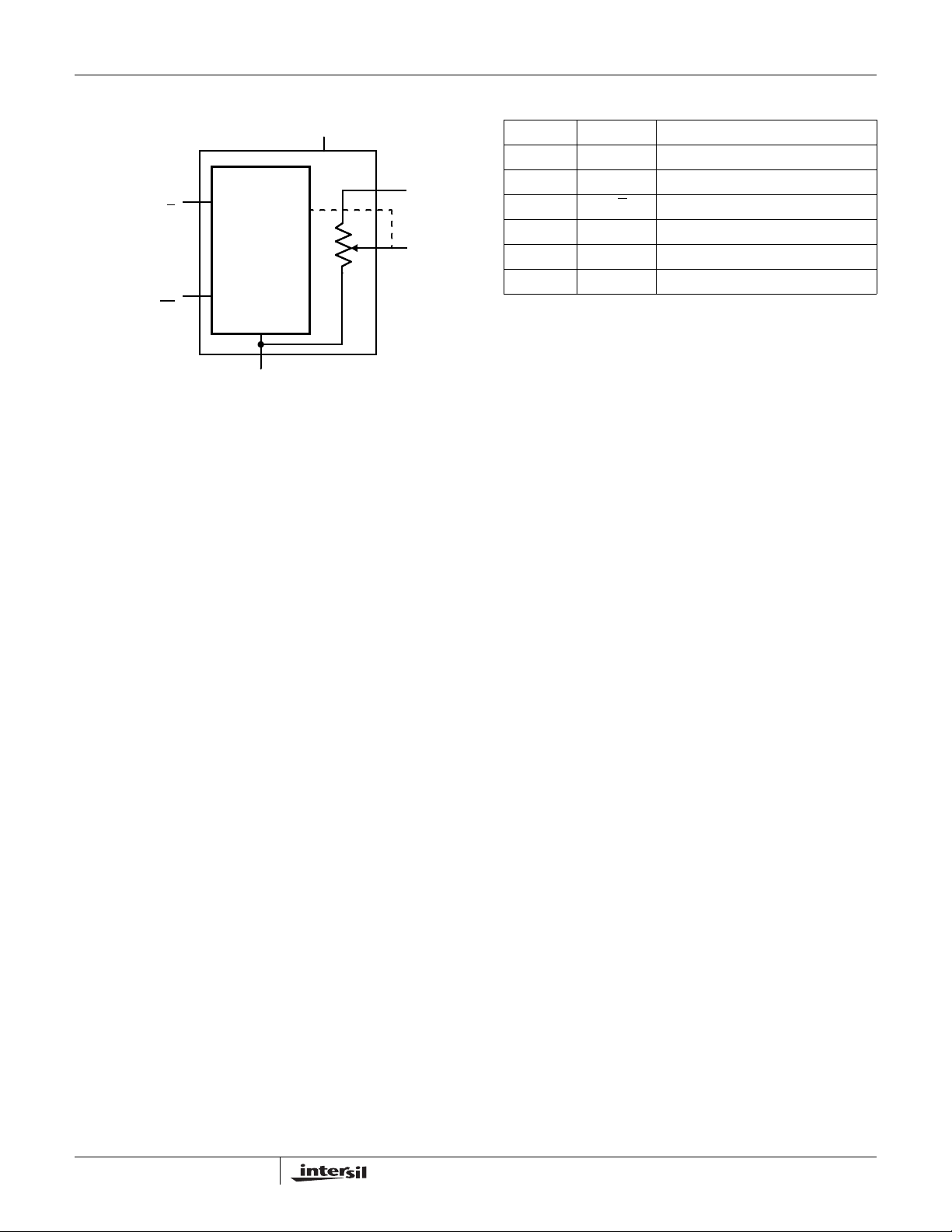
Block Diagram
UP/DOWN
(U/D
)
DEVICE SELECT
)
(CS
CONTROL
AND
MEMORY
GND (GROUND)
GENERAL
VCC
RH
RW
Pin Descriptions
6-PIN SYMBOL DESCRIPTION
1 VDD Supply voltage
2 GND Ground/Low terminal
3U/D
4CSChip select
5 RW Wiper terminal
6 RH High terminal
Up - Down
2
FN8230.3
October 7, 2005
Page 3
ISL90462
Absolute Maximum Ratings Recommended Operating Conditions
Storage Temperature . . . . . . . . . . . . . . . . . . . . . . . .-65°C to +150°C
Voltage on CS
, U/D and VCC With Respect to GND. . . . -1V to +7V
Lead Temperature (soldering 10s) . . . . . . . . . . . . . . . . . . . . . . 300°C
I
(10s) . . . . . . . . . . . . . . . . . . . . . . . . . . . . . . . . . . . . . . . . . . ±6mA
W
Power Rating . . . . . . . . . . . . . . . . . . . . . . . . . . . . . . . . . . . . . . .1mW
CAUTION: Stresses above those listed under “Absolute Maximum Ratings” may cause permanent damage to the device. This is a stress rating only; functional operation
of the device (at these or any other conditions above those listed in the operational sections of this specification) is not implied. Exposure to absolute maximum rating
conditions for extended periods may affect device reliability.
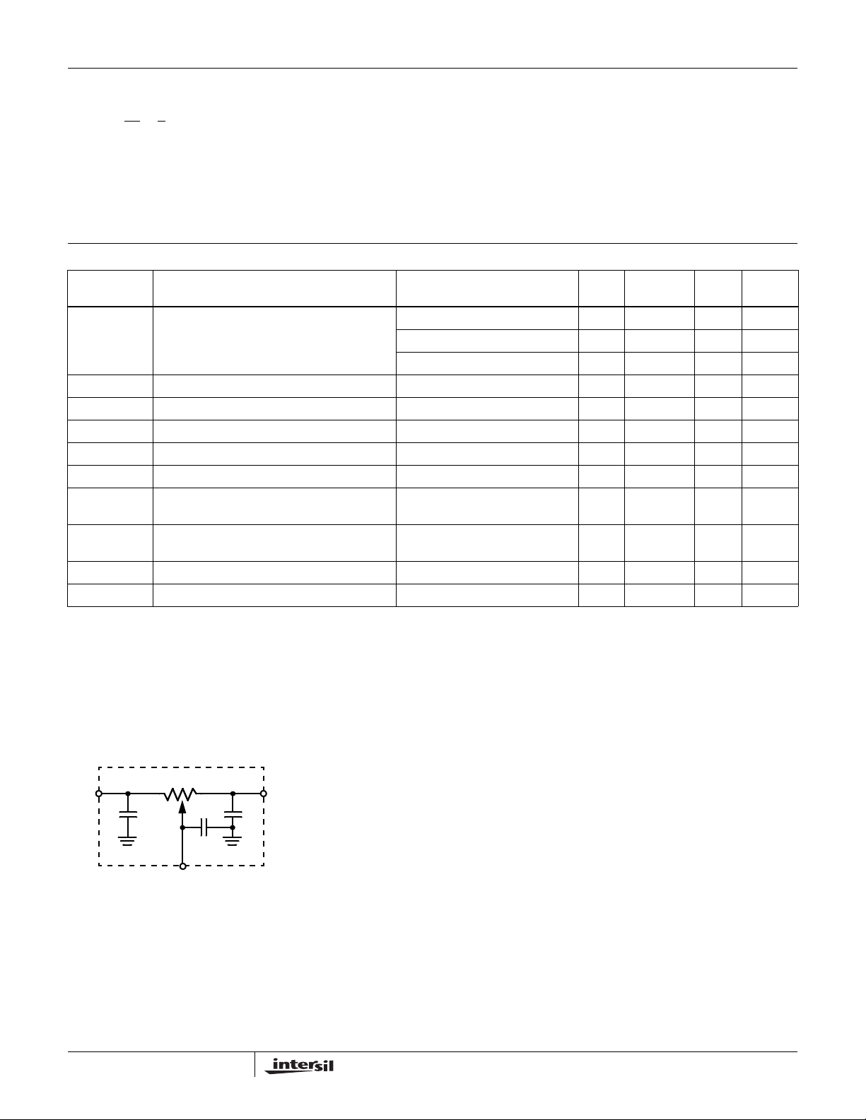
Potentiometer Specifications Over recommended operating conditions unless otherwise stated.
SYMBOL PARAMETER TEST CONDITIONS MIN
R
TOT
V
R
RW Wiper Resistance 600 Ω
I
W
C
H/CL/CW
NOTES:
1. Absolute linearity is utilized to determine actual wiper voltage versus expected voltage = (R
n = 1 .. 29 only
2. Relative linearity is a measure of the error in step size between taps = R
3. 1 Ml = Minimum Increment = R
4. Typical values are for T
End to end resistance W version 8 10 12 kΩ
U version 40 50 60 kΩ
T version 80 100 120 kΩ
RH, RL terminal voltages 0 V
Noise Ref: 1kHz -120 dBV
Wiper Current 0.6 mA
Resolution 132Taps
Absolute linearity (Note 1) R
Relative linearity (Note 2) R
R
temperature coefficient ±35 ppm/°C
TOTAL
H(n)(actual)-RH(n)(expected)
H(n+1)
Potentiometer capacitances See Equivalent Circuit 10/10/25 pF
/31.
TOT
= 25°C and nominal supply voltage.
A
Temperature Range (Industrial) . . . . . . . . . . . . . . . . . .-40°C to 85°C
V
. . . . . . . . . . . . . . . . . . . . . . . . . . . . . . . . . . . . . . . . 2.7V to 5.5V
CC
TYP
(Note 4) MAX UNIT
CC
±1 MI
(Note 3)
-[R
H
H(n) + MI
(n+1)
]±0.5MI
(Note 3)
(actual)-R
(n)
H
-[R
+ Ml] = ±0.5 Ml, n = 1 .. 29 only.
(n)
H
(expected)) = ±1 Ml Maximum.
(n)
H
V
Equivalent Circuit
R
TOTAL
R
H
C
H
C
R
W
R
L
W
C
L
3
FN8230.3
October 7, 2005
Page 4
ISL90462
DC Electrical Specifications Over recommended operating conditions unless otherwise specified.
TYP
SYMBOL PARAMETER TEST CONDITIONS MIN
I
I
V
V
C
CC
SB
I
LI
VCC active current (Increment) CS = 0V, U/D = f
Standby supply current CS = VCC, U/D = GND or V
CS input leakage current VIN = GND to V
CS, U/D input HIGH voltage V
IH
CS, U/D input LOW voltage V
IL
CS, U/D input capacitance VCC = 3V, VIN = GND, TA= 25°C, f = 1MHz 10 pF
IN
clock
CC
= 1MHz and V
= 3V 0.3 1 µA
CC
= 3V 25 µA
CC
CC
Timing Specifications Over recommended operating conditions unless otherwise specified
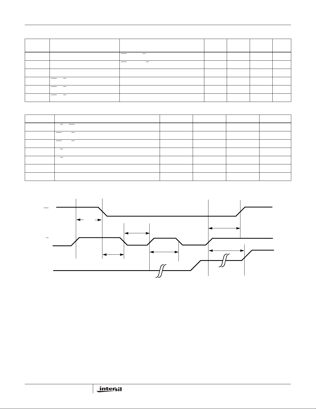
SYMBOL PARAMETER MIN TYP (Note 4) MAX UNIT
t
CU
t
CI
t
IC
t
lL
t
lH
f
TOGGLE
t
SETTLE
U/D to CS setup 25 ns
CS to U/D setup 50 ns
CS to U/D hold 25 ns
U/D LOW period 300 ns
U/D HIGH period 300 ns
Up/Down toggle Rate 1 MHz
Output settling time 1 µs
(NOTE 4)
MAX UNIT
±1 µA
x 0.7 V
x 0.3 V
CC
CS
U/D
RW
t
CU
t
IL
t
t
CI
IH
FIGURE 1. SERIAL INTERFACE TIMING DIAGRAM, INCREMENT
t
IC
t
SETTLE
4
FN8230.3
October 7, 2005
Page 5
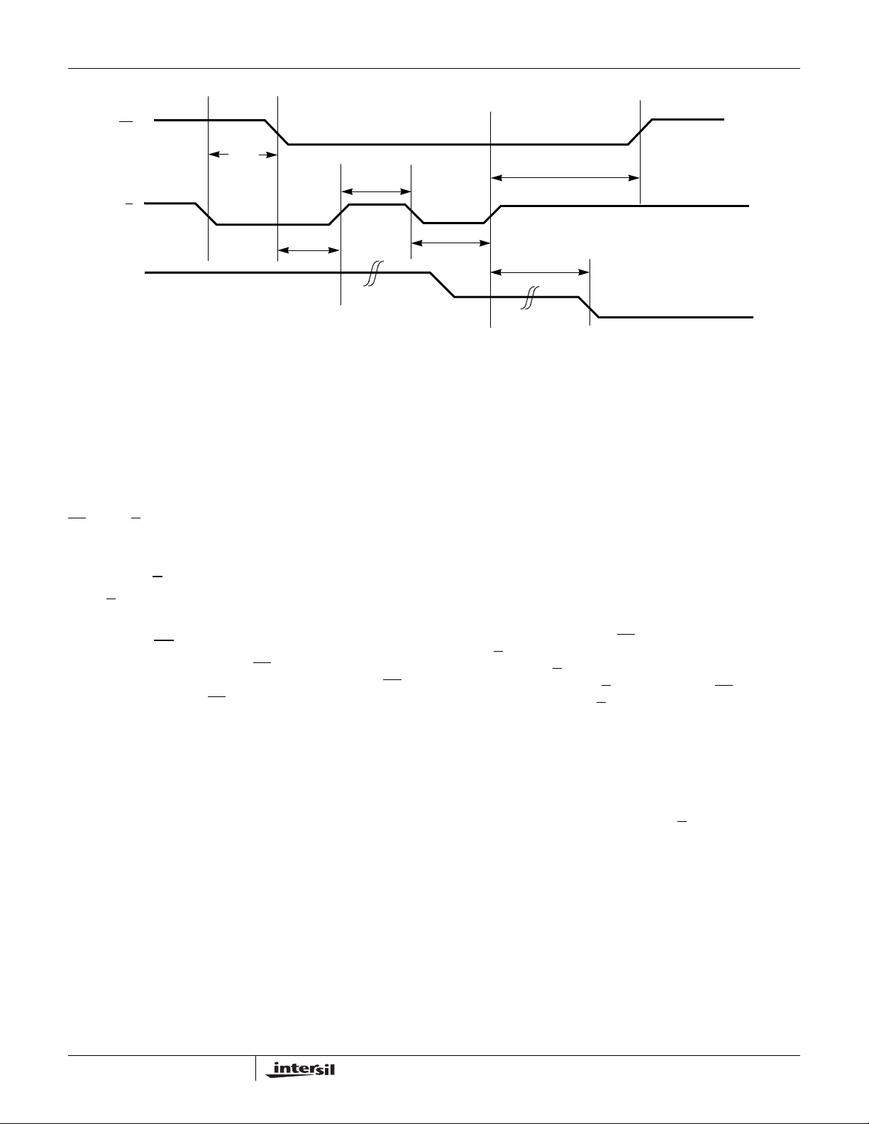
CS
U/D
RW
ISL90462
t
CU
t
IH
t
t
CI
FIGURE 2. SERIAL INTERFACE TIMING DIAGRAM DECREMENT
IL
t
SETTLE
t
IC
Pin Descriptions
RH and RW
The ISL90462 contains a digital potentiometer with one
terminal tied to the ground pin (GND) of the device. The RH
pin is the other potentiometer terminal, and the RW pin is the
wiper terminal. The position of the wiper is controlled by the
CS
- and U/D- inputs, with a movement "up" connecting the
wiper closer to the RH pin, and movement "down"
connection the wiper closer to the GND pin.
Up/Down (U/D)
The U/D input controls the direction of the wiper movement
and whether the counter is incremented or decremented.
Chip Select (CS)
The device is selected when the CS input is LOW. The
current counter value is stored in volatile memory when CS
is returned HIGH. When CS
low power standby mode.
is high, the device is placed in
Principles of Operation
There are two sections of the ISL90462: the input control,
counter and decode section; and the resistor array. The input
control section operates just like an up/down counter. The
output of this counter is decoded to turn on a single
electronic switch connecting a point on the resistor array to
the wiper output. The resistor array is comprised of 31
individual resistors connected in series. At either end of the
array and between each resistor is an electronic switch that
transfers the connection at that point to the wiper. The RH
and RW terminals are uncommitted, and can for a variable
voltage divider if RH is connected to a voltage source.
The direction of the wiper movement is defined when the
device is selected. If during CS
the U/D
rising edge of U/D
on each rising edge of U/D
input is LOW, the wiper will move down on each
toggling. Similarly, the wiper will move up
from High to Low, the U/D
The wiper, when at either fixed terminal, acts like its
mechanical equivalent and does not move beyond the last
position. That is, the counter does not wrap around when
clocked to either extreme.
If the wiper is moved several positions, multiple taps are
connected to the wiper for t
The 2-terminal resistance value for the device can
temporarily change by a significant amount if the wiper is
moved several positions.
transition from High to Low
toggling if, during CS transition
input is High.
SETTLE
(U/D to RW change).
5
FN8230.3
October 7, 2005
Page 6
ISL90462
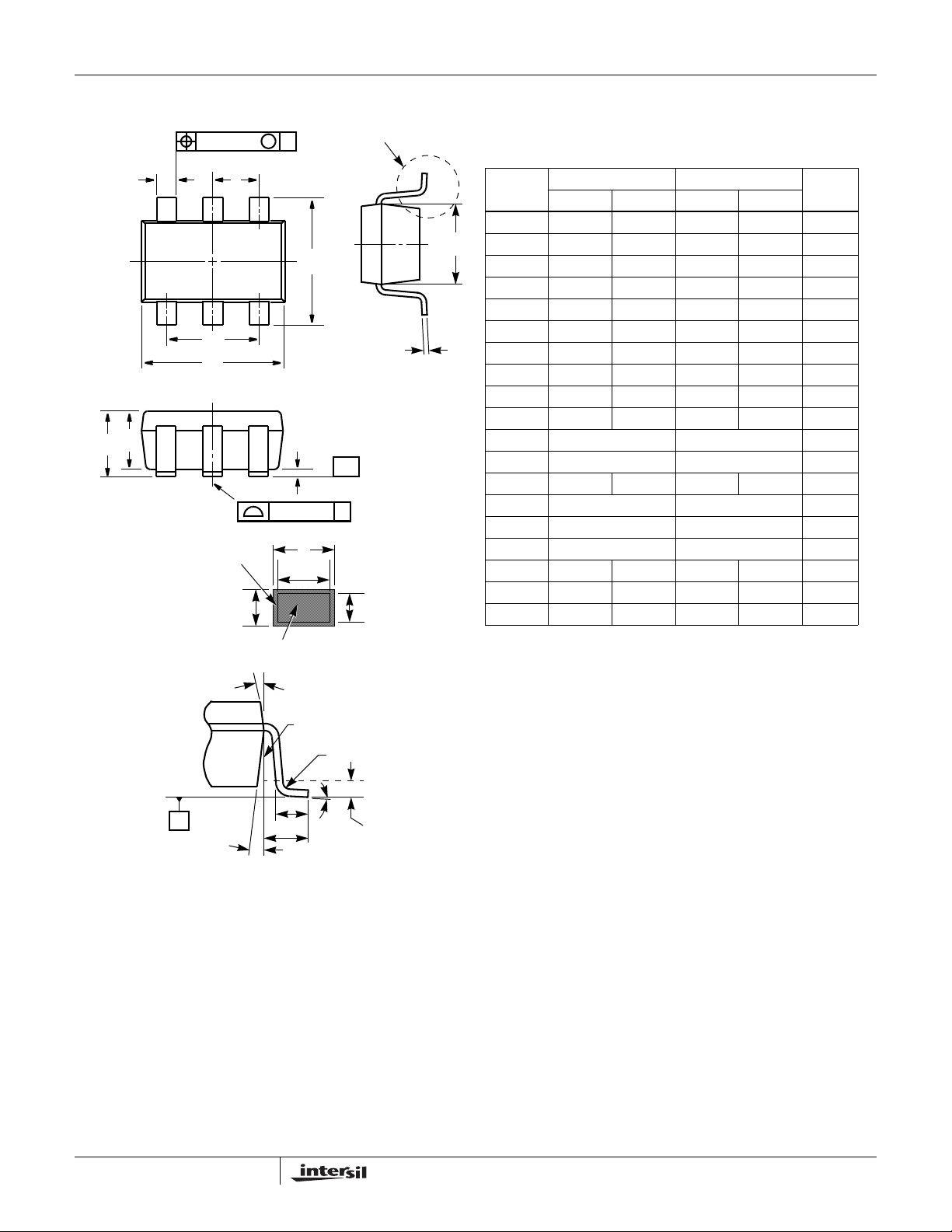
Small Outline Transistor Plastic Packages (SOT23-6)
C
L
A2
A
SEATING
PLANE
0.20 (0.008)
C
L
b
123
e1
D
C
L
WITH
PLATING
4X θ1
C
4X θ1
M
e
456
0.10 (0.004) C
c
BASE METAL
L1
C
VIEW C
P6.064
6 LEAD SMALL OUTLINE TRANSISTOR PLASTIC PACKAGE
INCHES MILLIMETERS
SYMBOL
NOTESMIN MAX MIN MAX
A 0.036 0.057 0.90 1.45 -
C
L
E
E1
A1 0.000 0.0059 0.00 0.15 A2 0.036 0.051 0.90 1.30 -
b 0.012 0.020 0.30 0.50 -
b1 0.012 0.018 0.30 0.45
c 0.003 0.009 0.08 0.22 6
C
c1 0.003 0.008 0.08 0.20 6
D 0.111 0.118 2.80 3.00 3
E 0.103 0.118 2.60 3.00 -
E1 0.060 0.068 1.50 1.75 3
A1
SEATING
PLANE
-C-
e 0.0374 Ref 0.95 Ref -
e1 0.0748 Ref 1.90 Ref -
L 0.014 0.022 0.35 0.55 4
L1 0.024 Ref. 0.60 Ref.
L2 0.010 Ref. 0.25 Ref.
b
b1
N6 65
R 0.004 - 0.10 -
R1 0.004 0.010 0.10 0.25
c1
α
o
0
o
8
o
0
o
8
-
Rev. 3 9/03
NOTES:
1. Dimensioning and tolerance per ASME Y14.5M-1994.
2. Package conforms to EIAJ SC-74 and JEDEC MO178AB.
3. Dimensions D and E1 are exclusive of mold flash, protrusions,
R1
or gate burrs.
4. Footlength L measured at reference to gauge plane.
R
GAUGE PLANE
L
α
L2
5. “N” is the number of terminal positions.
6. These Dimensions apply to the flat section of the lead between
0.08mm and 0.15mm from the lead tip.
7. Controlling dimension: MILLIMETER. Converted inch dimensions are for reference only
VIEW C
6
FN8230.3
October 7, 2005
Page 7
ISL90462
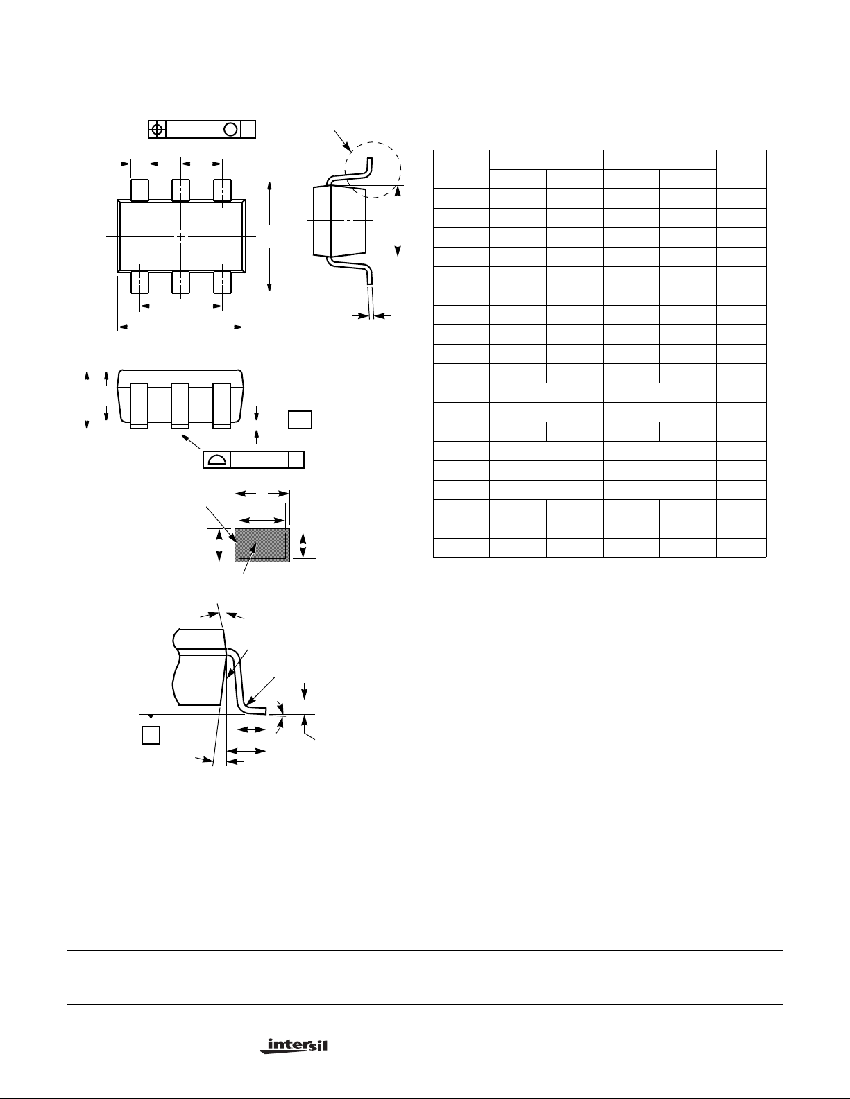
Small Outline Transistor Plastic Packages (SC70-6)
C
L
A2
A
SEATING
PLANE
0.20 (0.008)
C
L
b
123
e1
D
C
L
WITH
PLATING
4X θ1
C
4X θ1
M
e
456
0.10 (0.004) C
c
BASE METAL
L1
C
VIEW C
P6.049
6 LEAD SMALL OUTLINE TRANSISTOR PLASTIC PACKAGE
INCHES MILLIMETERS
SYMBOL
NOTESMIN MAX MIN MAX
A 0.031 0.043 0.80 1.10 -
C
L
E
E1
A1 0.000 0.004 0.00 0.10 A2 0.031 0.039 0.00 1.00 -
b 0.006 0.012 0.15 0.30 -
b1 0.006 0.010 0.15 0.25
c 0.003 0.009 0.08 0.22 6
C
c1 0.003 0.009 0.08 0.20 6
D 0.073 0.085 1.85 2.15 3
E 0.071 0.094 1.80 2.40 -
E1 0.045 0.053 1.15 1.35 3
A1
SEATING
PLANE
-C-
e 0.0256 Ref 0.65 Ref -
e1 0.0512 Ref 1.30 Ref -
L 0.010 0.018 0.26 0.46 4
L1 0.017 Ref. 0.420 Ref.
L2 0.006 BSC 0.15 BSC
b
b1
N6 65
R 0.004 - 0.10 -
R1 0.004 0.010 0.15 0.25
c1
α
o
0
o
8
o
0
o
8
-
Rev. 2 9/03
NOTES:
1. Dimensioning and tolerance per ASME Y14.5M-1994.
2. Package conforms to EIAJ SC70 and JEDEC MO203AB.
3. Dimensions D and E1 are exclusive of mold flash, protrusions,
R1
R
GAUGE PLANE
L
α
L2
or gate burrs.
4. Footlength L measured at reference to gauge plane.
5. “N” is the number of terminal positions.
6. These Dimensions apply to the flat section of the lead between
0.08mm and 0.15mm from the lead tip.
7. Controlling dimension: MILLIMETER. Converted inch dimensions are for reference only
VIEW C
All Intersil U.S. products are manufactured, assembled and tested utilizing ISO9000 quality systems.
Intersil Corporation’s quality certifications can be viewed at www.intersil.com/design/quality
Intersil products are sold by description only. Intersil Corporation reserves the right to make changes in circuit design, software and/or specifications at any time without
notice. Accordingly, the reader is cautioned to verify that data sheets are current before placing orders. Information furnished by Intersil is believed to be accurate and
reliable. However, no responsibility is assumed by Intersil or its subsidiaries for its use; nor for any infringements of patents or other rights of third parties which may result
from its use. No license is granted by implication or otherwise under any patent or patent rights of Intersil or its subsidiaries.
For information regarding Intersil Corporation and its products, see www.intersil.com
7
FN8230.3
October 7, 2005
 Loading...