

Page 1
®
www.BDTIC.com/Intersil
ISL9011A
Data Sheet March 7, 2008
Dual LDO with Low Noise, Low IQ and
High PSRR
ISL9011A is a high performance dual LDO capable of
sourcing 150mA current from Channel 1 and 300mA from
Channel 2. The device has a low standby current and
high-PSRR and is stable with output capacitance of 1µF to
10µF with ESR of up to 200mΩ.
A reference bypass pin allows an external capacitor for
adjusting a noise filter for low noise and high PSRR
applications.
The quiescent current is typically only 45µA with both LDOs
enabled and active. Separate enable pins control each
individual LDO output. When both enable pins are low, the
device is in shutdown, typically drawing less than 0.1µA.
Several combinations of voltage outputs are standard.
Output voltage options for each LDO range from 1.5V to
3.3V. Other output voltage options may be available upon
request.
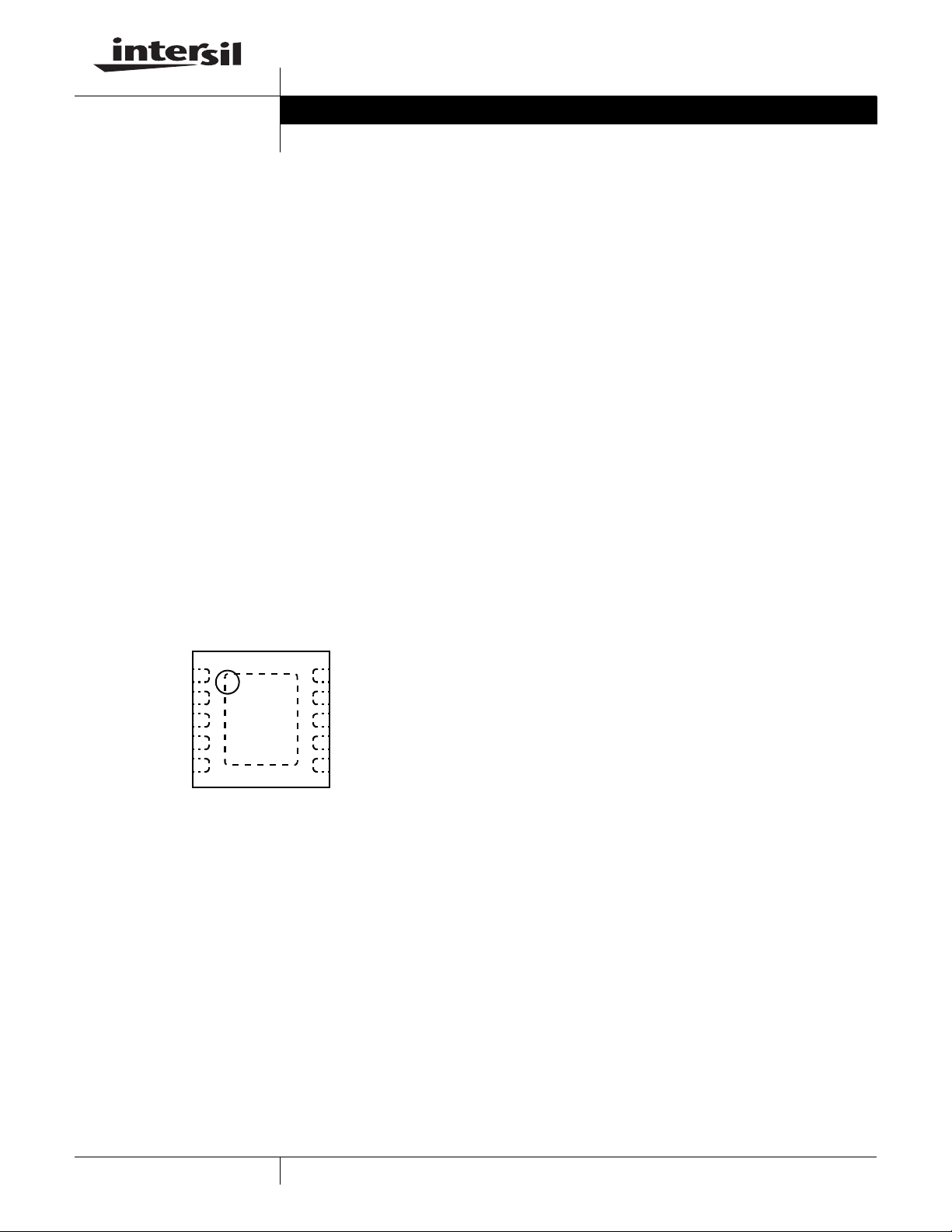
Pinout
ISL9011A
(10 LD 3x3 DFN)
TOP VIEW
VIN
EN1
EN2
CBYP
NC
1
2
3
4
5
10
VO1
9
VO2
8
NC
NC
7
6
GND
FN6437.1
Features
• Integrates two high performance LDOs
- VO1 - 150mA output
- VO2 - 300mA output
• Excellent transient response to large current steps
• Excellent load regulation: <1% voltage change across full
range of load current
• High PSRR: 70dB @ 1kHz
• Wide input voltage capability: 2.3V to 6.5V
• Extremely low quiescent current: 45µA (both LDOs active)
• Low dropout voltage: typically 120mV @ 150mA
• Low output noise: typically 30µV
@ 100µA (1.5V)
RMS
• Stable with 1µF to 10µF ceramic capacitors
• Separate enable pins for each LDO
• Soft-start to limit input current surge during enable
• Current limit and overheat protection
• ±1.8% accuracy over all operating conditions
• Tiny 10 Ld 3mmx3mm DFN package
• -40°C to +85°C operating temperature range
• Pin compatible with Micrel MIC2211
• Pb-free (RoHS compliant)
Applications
• PDAs, Cell Phones and Smart Phones
• Portable Instruments, MP3 Players
• Handheld Devices including Medical Handhelds
1
CAUTION: These devices are sensitive to electrostatic discharge; follow proper IC Handling Procedures.
1-888-INTERSIL or 1-888-468-3774
| Intersil (and design) is a registered trademark of Intersil Americas Inc.
All other trademarks mentioned are the property of their respective owners.
Copyright © Intersil Americas Inc. 2007, 2008. All Rights Reserved.
Page 2
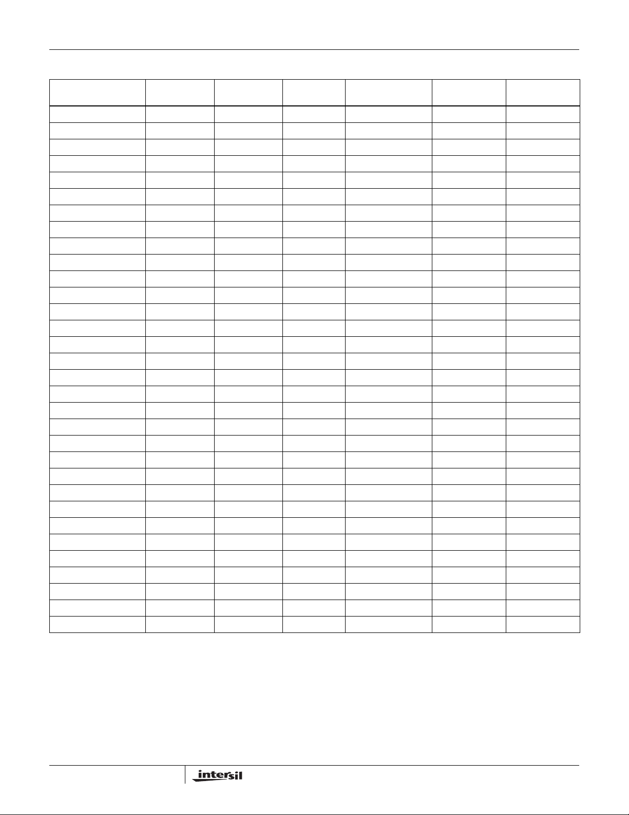
Ordering Information
www.BDTIC.com/Intersil
ISL9011A
PART NUMBER
(Notes 1, 2, 3) PART MARKING
ISL9011AIRNNZ DGPA 3.3 3.3 -40 to +85 10 Ld 3x3 DFN L10.3x3C
ISL9011AIRNJZ DGNA 3.3 2.8 -40 to +85 10 Ld 3x3 DFN L10.3x3C
ISL9011AIRNFZ DGMA 3.3 2.5 -40 to +85 10 Ld 3x3 DFN L10.3x3C
ISL9011AIRNCZ DGLA 3.3 1.8 -40 to +85 10 Ld 3x3 DFN L10.3x3C
ISL9011AIRMNZ DGKA 3.0 3.3 -40 to +85 10 Ld 3x3 DFN L10.3x3C
ISL9011AIRMMZ DGJA 3.0 3.0 -40 to +85 10 Ld 3x3 DFN L10.3x3C
ISL9011AIRMGZ DGHA 3.0 2.7 -40 to +85 10 Ld 3x3 DFN L10.3x3C
ISL9011AIRLLZ DGGA 2.9 2.9 -40 to +85 10 Ld 3x3 DFN L10.3x3C
ISL9011AIRKNZ DGEA 2.85 3.3 -40 to +85 10 Ld 3x3 DFN L10.3x3C
ISL9011AIRKKZ DGDA 2.85 2.85 -40 to +85 10 Ld 3x3 DFN L10.3x3C
ISL9011AIRKJZ DGCA 2.85 2.8 -40 to +85 10 Ld 3x3 DFN L10.3x3C
ISL9011AIRKFZ DGBA 2.85 2.5 -40 to +85 10 Ld 3x3 DFN L10.3x3C
ISL9011AIRKPZ DGFA 2.85 1.85 -40 to +85 10 Ld 3x3 DFN L10.3x3C
ISL9011AIRKCZ DFYA 2.85 1.8 -40 to +85 10 Ld 3x3 DFN L10.3x3C
ISL9011AIRJNZ DFVA 2.8 3.3 -40 to +85 10 Ld 3x3 DFN L10.3x3C
ISL9011AIRJMZ DFTA 2.8 3.0 -40 to +85 10 Ld 3x3 DFN L10.3x3C
ISL9011AIRJRZ DWFA 2.8 2.6 -40 to +85 10 Ld 3x3 DFN L10.3x3C
ISL9011AIRJCZ DFSA 2.8 1.8 -40 to +85 10 Ld 3x3 DFN L10.3x3C
ISL9011AIRJBZ DFRA 2.8 1.5 -40 to +85 10 Ld 3x3 DFN L10.3x3C
ISL9011AIRGPZ DFPA 2.7 1.85 -40 to +85 10 Ld 3x3 DFN L10.3x3C
ISL9011AIRGCZ DFNA 2.7 1.8 -40 to +85 10 Ld 3x3 DFN L10.3x3C
ISL9011AIRFJZ DFMA 2.5 2.8 -40 to +85 10 Ld 3x3 DFN L10.3x3C
ISL9011AIRFDZ DFLA 2.5 2.0 -40 to +85 10 Ld 3x3 DFN L10.3x3C
ISL9011AIRFCZ DFKA 2.5 1.8 -40 to +85 10 Ld 3x3 DFN L10.3x3C
ISL9011AIRPLZ DGRA 1.85 2.9 -40 to +85 10 Ld 3x3 DFN L10.3x3C
ISL9011AIRPPZ DGSA 1.85 1.85 -40 to +85 10 Ld 3x3 DFN L10.3x3C
ISL9011AIRCJZ DFJA 1.8 2.8 -40 to +85 10 Ld 3x3 DFN L10.3x3C
ISL9011AIRCCZ DFHA 1.8 1.8 -40 to +85 10 Ld 3x3 DFN L10.3x3C
ISL9011AIRBLZ DFGA 1.5 2.9 -40 to +85 10 Ld 3x3 DFN L10.3x3C
ISL9011AIRBJZ DFFA 1.5 2.8 -40 to +85 10 Ld 3x3 DFN L10.3x3C
ISL9011AIRBCZ DFEA 1.5 1.8 -40 to +85 10 Ld 3x3 DFN L10.3x3C
ISL9011AIRBBZ DFDA 1.5 1.5 -40 to +85 10 Ld 3x3 DFN L10.3x3C
NOTES:
1. Add “-T” suffix for tape and reel. Please refer to TB347 for details on reel specifications.
2. For availability and lead time of devices with voltage combinations not listed in the table, contact Intersil Marketing.
3. These Intersil Pb-free plastic packaged products employ special Pb-free material sets; molding compounds/die attach materials and 100% matte
tin plate PLUS ANNEAL - e3 termination finish, which is RoHS compliant and compatible with both SnPb and Pb-free soldering operations.
Intersil Pb-free products are MSL classified at Pb-free peak reflow temperatures that meet or exceed the Pb-free requirements of IPC/JEDEC
J STD-020.
VO1 VOLTAGE
(V)
VO2 VOLTAGE
(V) TEMP RANGE (°C)
PACKAGE
(Pb-free) PKG. DWG. #
2
FN6437.1
March 7, 2008
Page 3
ISL9011A
www.BDTIC.com/Intersil
Absolute Maximum Ratings Thermal Information
Supply Voltage (VIN) . . . . . . . . . . . . . . . . . . . . . . . . . . . . . . . . +7.1V
V
1, VO2 Pins. . . . . . . . . . . . . . . . . . . . . . . . . . . . . . . . . . . . . +3.6V
O
All Other Pins . . . . . . . . . . . . . . . . . . . . . . . . . . -0.3 to (V
IN
+ 0.3)V
Recommended Operating Conditions
Ambient Temperature Range (TA) . . . . . . . . . . . . . . .-40°C to +85°C
Supply Voltage (VIN) . . . . . . . . . . . . . . . . . . . . . . . . . . .2.3V to 6.5V
CAUTION: Do not operate at or near the maximum ratings listed for extended periods of time. Exposure to such conditions may adversely impact product reliability and
result in failures not covered by warranty.
NOTES:
is measured in free air with the component mounted on a high effective thermal conductivity test board with “direct attach” features. See
4. θ
JA
Tech Brief TB379.
5. For θ
, the “case temp” location is the center of the exposed metal pad on the package underside.
JC
Thermal Resistance (Notes 4, 5) θ
10 Ld 3x3 DFN Package . . . . . . . . . . . 50 10
Junction Temperature Range . . . . . . . . . . . . . . . . .-40°C to +125°C
Operating Temperature Range . . . . . . . . . . . . . . . . .-40°C to +85°C
Storage Temperature Range . . . . . . . . . . . . . . . . . .-65°C to +150°C
Pb-free reflow profile . . . . . . . . . . . . . . . . . . . . . . . . . .see link below
http://www.intersil.com/pbfree/Pb-FreeReflow.asp
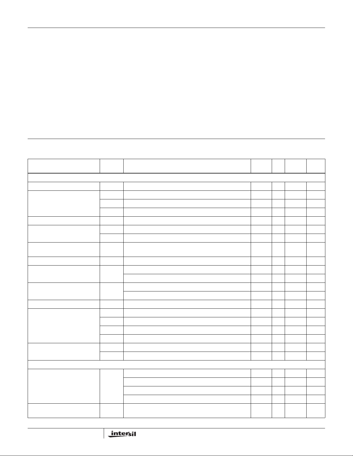
Electrical Specifications Unless otherwise noted, all parameters are guaranteed over the operational supply voltage and temperature
range of the device as follows: T
C
= 1µF; CO = 1µF; C
IN
PARAMETER SYMBOL TEST CONDITIONS
DC CHARACTERISTICS
Supply Voltage V
Ground Current Quiescent condition: I
Shutdown Current I
UVLO Threshold V
Regulation Voltage Accuracy Variation from nominal voltage output, V
Line Regulation V
Load Regulation I
Maximum Output Current I
Internal Current Limit I
Dropout Voltage (Note 6) V
Thermal Shutdown Temperature T
AC CHARACTERISTICS
Ripple Rejection I
Output Noise Voltage I
IN
I
DD1
I
DD2
DDS
UV+
V
UV-
MAX
LIM
DO1IO
V
DO2IO
V
DO3IO
V
DO4IO
SD+
T
SD-
One LDO active 25 40 µA
Both LDO active 45 60 µA
@ +25°C 0.1 1.0 µA
T
= -40°C to +125°C
J
IN
OUT
I
OUT
VO1: Continuous 150 mA
VO2: Continuous 300 mA
= 150mA; VO > 2.1V (VO1) 125 200 mV
= 300mA; VO < 2.5V (VO2) 300 500 mV
= 300mA; 2.5V ≤ VO ≤ 2.8V (VO2) 250 400 mV
= 300mA; VO > 2.8V (VO2) 200 325 mV
= 10mA, VIN = 2.8V(min), VO = 1.8V, C
O
@ 1kHz 70 dB
@ 10kHz 55 dB
@ 100kHz 40 dB
= 100μA, VO = 1.5V, TA = +25°C, C
O
BW = 10Hz to 100kHz
BYP
= (V
OUT
= 100µA to 150mA (VO1 and VO2) 0.1 0.7 %
= 100µA to 300mA (VO2) 1.0 %
= -40°C to +85°C; VIN = (VO + 1.0V) to 6.5V with a minimum VIN of 2.3V;
A
= 0.01µF
MIN
(Note 7) TYP
2.3 6.5 V
= 0µA; IO2 = 0µA
O1
1.9 2.1 2.3 V
1.6 1.8 2.0 V
= VO+ 0.5 to 5.5V ,
IN
+ 1.0V relative to highest output voltage) to 5.5V -0.2 0 0.2 %/V
= 0.1µF
BYP
= 0.1µF
BYP
-1.8 +1.8 %
350 475 600 mA
(°C/W) θJC (°C/W)
JA
MAX
(Note 7) UNITS
145 °C
110 °C
30 µV
RMS
3
FN6437.1
March 7, 2008
Page 4
ISL9011A
www.BDTIC.com/Intersil
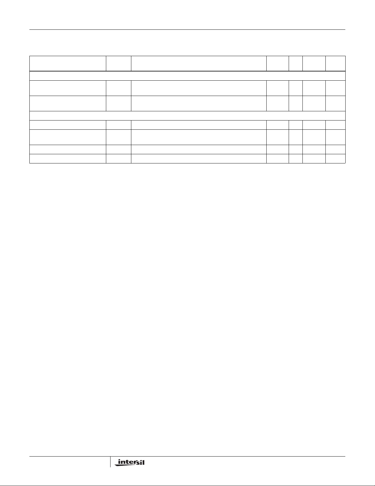
Electrical Specifications Unless otherwise noted, all parameters are guaranteed over the operational supply voltage and temperature
range of the device as follows: T
= 1µF; CO = 1µF; C
C
IN
PARAMETER SYMBOL TEST CONDITIONS
DEVICE START-UP CHARACTERISTICS
Device Enable Time t
LDO Soft-Start Ramp Rate t
EN1, EN2 PIN CHARACTERISTICS
Input Low Voltage V
Input High Voltage V
Input Leakage Current I
Pin Capacitance C
NOTE:
6. VOx = 0.98*VOx(NOM); Valid for VOx greater than 1.85V.
7. Parts are 100% tested at +25°C. Temperature limits established by characterization and are not production tested.
IL
Time from assertion of the ENx pin to when the output voltage
EN
reaches 95% of the VO(nom)
Slope of linear portion of LDO output voltage ramp during
SSR
start-up
IL
IH
, I
IH
Informative 5 pF
PIN
BYP
= -40°C to +85°C; VIN = (VO + 1.0V) to 6.5V with a minimum VIN of 2.3V;
A
= 0.01µF (Continued)
MIN
(Note 7) TYP
-0.3 0.5 V
1.4 VIN+
MAX
(Note 7) UNITS
250 500 µs
30 60 µs/V
0.3
0.1 µA
V
4
FN6437.1
March 7, 2008
Page 5
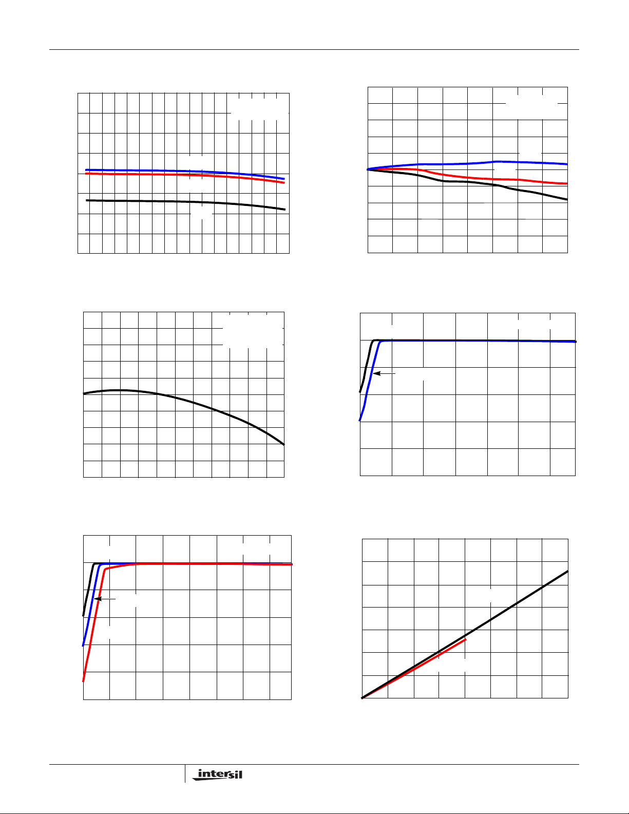
Typical Performance Curves
www.BDTIC.com/Intersil
0.8
0.6
0.4
(%)
O
0.2
0.0
-0.2
-0.4
OUTPUT VOLTAGE, V
-0.6
-0.8
3.8 4.2 6.25.8
INPUT VOLTAGE (V)
FIGURE 1. OUTPUT VOLT A GE vs INPUT VOL TAGE
(3.3V OUTPUT)
-40°C
+25°C
+85°C
VO = 3.3V
I
= 0mA
LOAD
ISL9011A
6.63.4 4.6 5.0 5.4
0.10
+25°C
(mA)
O
VIN = 3.8V
V
= 3.3V
O
-40°C
-0.02
-0.04
-0.06
OUTPUT VOLTAGE CHANGE (%)
-0.08
-0.10
0.08
0.06
0.04
0.02
0.00
+85°C
50 150 250 350
100 200 300 4000
LOAD CURRENT - I
FIGURE 2. OUTPUT VOLTAGE CHANGE vs LOAD CURRENT
0.10
0.08
0.06
0.04
0.02
0.00
-0.02
-0.04
-0.06
OUTPUT VOLTAGE CHANGE (%)
-0.08
-0.10
V
= 3.8V
IN
= 3.3V
V
O
I
= 0mA
LOAD
-10 20 50 110-40
-25 5 35 8065 95 125
TEMPERATURE (°C)
3.4
IO = 0mA
3.3
(V)
O
3.2
3.1
3.0
OUTPUT VOLTAGE, V
2.9
2.8
3.1 3.6 4.1 4.6 5.1 6.15.6
IO = 150mA
INPUT VOLTAGE (V)
VO1 = 3.3V
FIGURE 3. OUTPUT VOLTAGE CHANGE vs TEMPERATURE FIGURE 4. OUTPUT VOL T AGE vs INPUT VOLTAGE
(V
1=3.3V)
O
2.9
2.8
(V)
O
2.7
2.6
2.5
OUTPUT VOLTAGE, V
2.4
IO = 0mA
IO = 300mA
VO2 = 2.8V
IO = 150mA
350
300
(mV)
250
DO
200
150
100
DROPOUT VOLTAGE, V
50
VO1 = 3.3V
VO2 = 2.8V
6.5
2.3
2.63.13.64.14.65.1 6.1
INPUT VOLTAGE (V)
5.6
FIGURE 5. OUTPUT VOLT AGE vs INPUT VOL T AGE
2=2.8V)
(V
O
6.5
0
50 100 150 200 250 300 350 4000
FIGURE 6. DROPOUT VOLTAGE vs LOAD CURRENT
5
OUTPUT LOAD (mA)
FN6437.1
March 7, 2008
Page 6
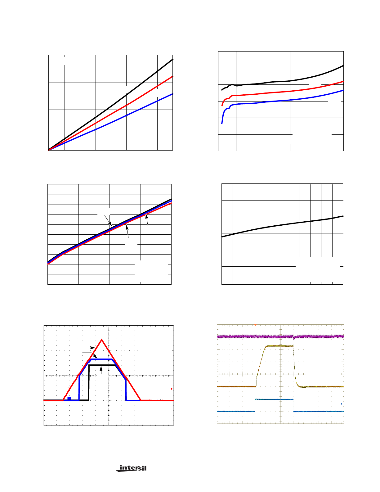
Typical Performance Curves (Continued)
www.BDTIC.com/Intersil
ISL9011A
175
VO1 = 3.3V
150
(mV)
125
DO
100
75
50
DROPOUT VOLTAGE, V
25
0
25 50 75 100 125 150 175 2000
OUTPUT LOAD (mA)
+85°C
+25°C
-40°C
55
50
+125°C
45
40
35
GROUND CURRENT (µA)
30
25
3.0 3.5 4.58 5.5 6.0
4.0 5.0 6.5
INPUT VOLTAGE (V)
VO1 = 3.3V
V
O
IO(BOTH CHANNELS) = 0µA
+25°C
2 = 2.8V
FIGURE 7. VO1 DROPOUT VOLTAGE vs LOAD CURRENT FIGURE 8. GROUND CURRENT vs INPUT VOLTAGE
200
180
160
140
120
100
80
60
GROUND CURRENT (µA)
40
20
0
FIGURE 9. GROUND CURRENT vs LOAD
+85°C
+25°C
-40°C
V
= 3.8V
IN
VO1 = 3.3V
VO2 = 2.8V
50 100 150 200 250 4000
LOAD CURRENT (mA)
350300
55
50
45
40
35
GROUND CURRENT (µA)
30
25
-25 5 35 8065 95 125
-10 20 50 110-40
TEMPERATURE (°C)
VIN = 3.8V
V
= 3.3V
O
= 0µA
I
LOAD
BOTH OUTPUTS ON
FIGURE 10. GROUND CURRENT vs TEMPERATURE
-40°C
VO1 = 3.3V
V
2 = 2.8V
5
5
VIN
V
4
4
3
3
2
2
1
1
VOLTAGE (V)
VOLTAGE (V)
0
0
0
0
1234567 10
1234567 10
VO1
V
O1
IN
VO2
VO2
TIME (s)
TIME (s)
O
I
1 = 150mA
L
I
2 = 300mA
L
89
89
FIGURE 11. POWER-UP/POWER-DOWN
VO2 (10mV/DIV)
3
2
1 (V)V
1
O
V
0
5
(V)
EN
0
100 200 300 400 500 600 700 8000
FIGURE 12. TURN-ON/TURN-OFF RESPONSE
6
TIME (µs)
VIN = 5.0V
VO1 = 3.3V
VO2 = 2.8V
IL1 = 150mA
IL2 = 300mA
C
-1, CL-2 = 1µF
L
C
= 0.01µF
BYP
March 7, 2008
900 1000
FN6437.1
Page 7
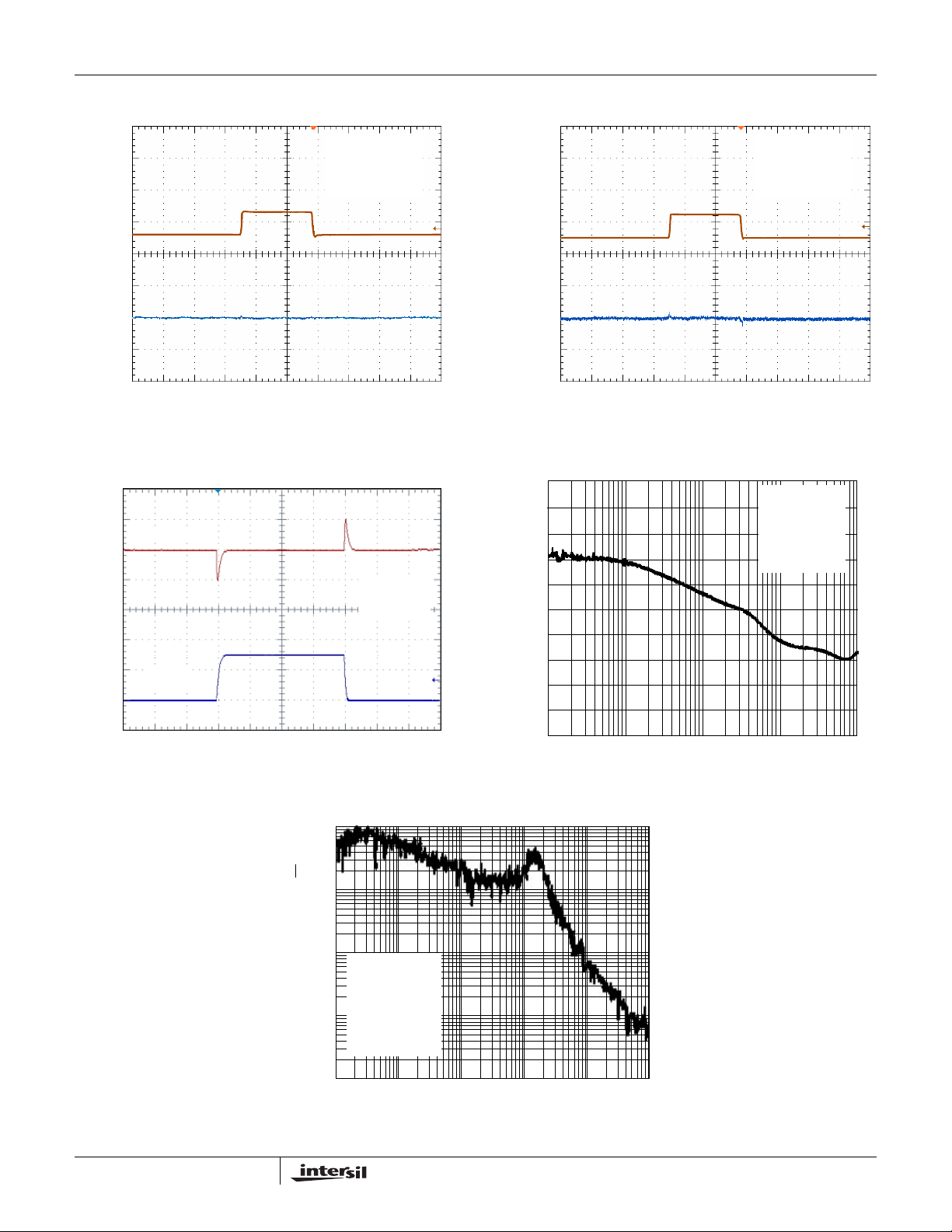
Typical Performance Curves (Continued)
www.BDTIC.com/Intersil
VO1 = 3.3V
VO1 = 3.3V
I
I
= 150mA
= 150mA
LOAD
LOAD
C
C
= 1μF
= 1µF
LOAD
LOAD
C
C
= 0.01μF
= 0.01µF
BYP
BYP
4.3V
4.3V
3.6V
3.6V
10mV/DIV
10mV/DIV
ISL9011A
4.2V
4.2V
3.5V
3.5V
10mV/DIV
10mV/DIV
VO2 = 2.8V
VO2 = 2.8V
I
I
= 300mA
= 300mA
LOAD
LOAD
= 1µF
= 1µF
C
C
LOAD
LOAD
C
C
= 0.01µF
= 0.01µF
BYP
BYP
400µs/DIV
400µs/DIV
400µs/DIV
FIGURE 13. LINE TRANSIENT RESPONSE, 3.3V OUTPUT FIGURE 14. LINE TRANSIENT RESPONSE, 2.8V OUTPUT
300mA
100µA
VO (25mV/DIV)
V
O
VIN = 2.8V
I
LOAD
100µs/DIV
FIGURE 15. LOAD TRANSIENT RESPONSE
1000
= 1.8V
100
90
80
70
60
50
PSRR (dB)
40
30
20
10
0
0.1 1k 10k 100k 1M
FREQUENCY (Hz)
FIGURE 16. PSRR vs FREQUENCY
VIN = 3.6V
= 1.8V
V
O
= 10mA
I
O
= 0.1µF
C
BYP
= 1µF
C
LOAD
100
10
VIN = 3.6V
VO = 1.8V
I
= 10mA
LOAD
= 0.1µF
C
1
BYP
CIN = 1µF
C
= 1µF
SPECTRAL NOISE DENSITY (nV/√Hz)
LOAD
0.1
10 100 1k 10k 100k 1M
FREQUENCY (Hz)
FIGURE 17. SPECTRAL NOISE DENSITY vs FREQUENCY
7
FN6437.1
March 7, 2008
Page 8
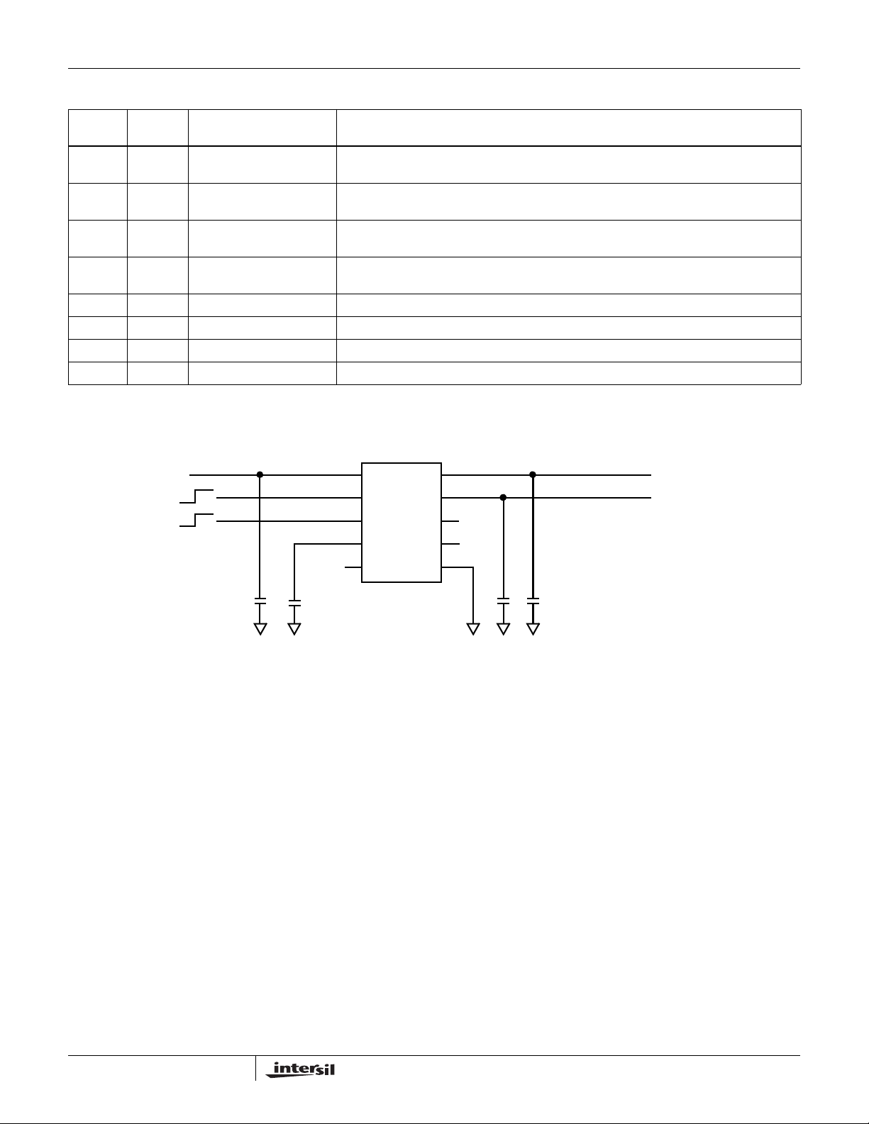
Pin Descriptions
www.BDTIC.com/Intersil
ISL9011A
PIN
NUMBER
1 VIN Analog I/O Supply Voltage/LDO Input:
2 EN1 Low Voltage Compatible
3 EN2 Low Voltage Compatible
4 CBYP Analog I/O Reference Bypass Capacitor Pin: Optionally connect capacitor of value 0.01µF to 1µF
5, 7, 8 NC NC No Connection
6 GND Ground GND is the connection to system ground. Connect to PCB Ground plane.
9VO2
10 VO1 Analog I/O LDO-1 Output: Connect capacitor of value 1µF to 10µF to GND (1µF recommended).
PIN
NAME TYPE DESCRIPTION
Connect a 1µF capacitor to GND.
LDO-1 Enable.
CMOS Input
LDO-2 Enable.
CMOS Input
between this pin and GND to tune in the desired noise and PSRR performance.
Analog I/O LDO-2 Output: Connect capacitor of value 1µF to 10µF to GND (1µF recommended).
Typical Application
VIN (2.3V TO 6.5V)
ENABLE 1
ENABLE 2
OFF
OFF
ON
ON
ISL9011A
1
VIN
2
EN1
3
EN2
4
CBYP
5
NC
C1 C2 C3 C4
VO1
VO2
NC
NC
GND
10
9
8
7
6
VOUT 1
VOUT 2
C1, C3, C4: 1µF X5R CERAMIC CAPACITOR
C2: 0.1µF X5R CERAMIC CAPACITOR
8
FN6437.1
March 7, 2008
Page 9
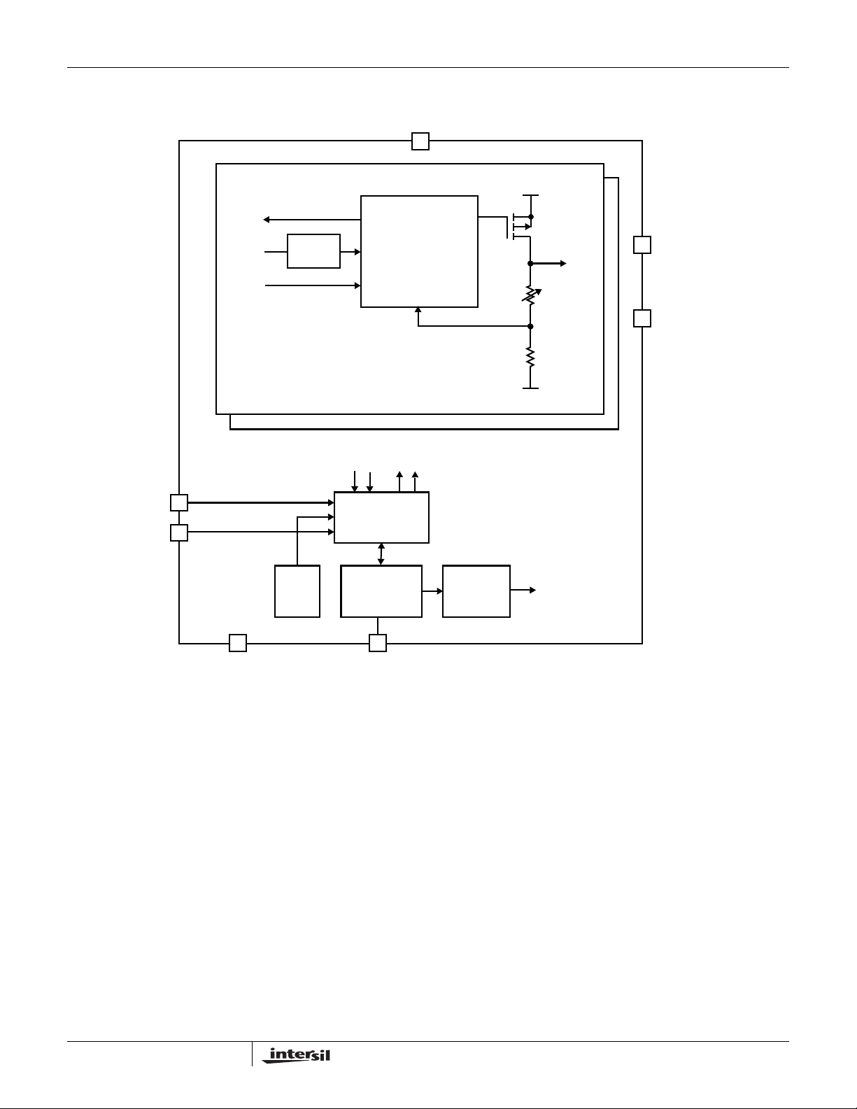
Block Diagram
www.BDTIC.com/Intersil
IS1
1V
QEN1
VREF
TRIM
ISL9011A
VIN
LDO
ERROR
AMPLIFIER
VO1
VO1
LDO-1
LDO-2
IS1
IS2
EN1
EN2
UVLO
CONTROL
LOGIC
BANDGAP AND
TEMPERATURE
SENSOR
CBYPGND
Functional Description
The ISL9011A contains all circuitry required to implement
two high performance LDOs. High performance is achieved
through a circuit that delivers fast transient response to
varying load conditions. In a quiescent condition, the
ISL9011A adjusts its biasing to achieve the lowest standby
current consumption.
The device also integrates current limit protection, smart
thermal shutdown protection, staged turn-on and soft-start.
Smart Thermal shutdown protects the device against
overheating. Staged turn-on and soft-start minimize start-up
input current surges without causing excessive device
turn-on time.
Power Control
The ISL9011A has two separate enable pins (EN1 and EN2)
to individually control power to each of the LDO outputs.
When both EN1 and EN2 are low, the device is in shutdown
QEN1
VO2
QEN2
VOLTAGE
REFERENCE
GENERATOR
~1.0V
1.00V
mode. During this condition, all on-chip circuits are off, and
the device draws minimum current, typically less than 0.1µA.
When one or both of the enable pins are asserted, the
device first polls the output of the UVLO detector to ensure
that VIN voltage is at least about 2.1V. Once verified, the
device initiates a start-up sequence. During the start-up
sequence, trim settings are first read and latched. Then,
sequentially, the bandgap, reference voltage and current
generation circuitry power-up. Once the references are
stable, a fast-start circuit quickly charges the external
reference bypass capacitor (connected to the CBYP pin) to
the proper operating voltage. After the bypass capacitor has
been charged, the LDO’s power-up.
If EN1 is brought high, and EN2 goes high before the VO1
output stabilizes, the ISL9011A delays the VO2 turn-on until
the VO1 output reaches its target level.
If EN2 is brought high, and EN1 goes high before VO2 starts
its output ramp, then VO1 turns on first and the ISL9011A
9
FN6437.1
March 7, 2008
Page 10

ISL9011A
www.BDTIC.com/Intersil
delays the VO2 turn-on until the VO1 output reaches its
target level.
If EN2 is brought high, and EN1 goes high after VO2 starts
its output ramp, then the ISL9011A immediately starts to
ramp up the VO1 output.
If both EN1 and EN2 are brought high at the same time, the
VO1 output has priority, and is always powered up first.
During operation, whenever the VIN voltage drops below
about 1.8V, the ISL9011A immediately disables both LDO
outputs. When VIN rises back above 2.1V, the device
re-initiates its start-up sequence and LDO operation will
resume automatically.
Reference Generation
The reference generation circuitry includes a trimmed
bandgap, a trimmed voltage reference divider, a trimmed
current reference generator, and an RC noise filter. The filter
includes the external capacitor connected to the CBYP pin.
A 0.01µF capacitor connected CBYP implements a 100Hz
lowpass filter, and is recommended for most high
performance applications. For the lowest noise application, a
0.1µF or greater CBYP capacitor should be used. This filters
the reference noise to below the 10Hz to 1kHz frequency
band, which is crucial in many noise-sensitive applications.
The bandgap generates a zero temperature coefficient (TC)
voltage for the reference divider. The reference divider
provides the regulation reference and other voltage
references required for current generation and
over-temperature detection.
The current generator outputs references required for
adaptive biasing as well as references for LDO output
current limit and thermal shutdown determination.
LDO Regulation and Programmable Output Divider
The LDO Regulator is implemented with a high-gain
operational amplifier driving a PMOS pass transistor. The
design of the ISL9011A provides a regulator that has low
quiescent current, fast transient response, and overall
stability across all operating and load current conditions.
LDO stability is guaranteed for a 1µF to 10µF output
capacitor that has a toleranc e better than 2 0% and ESR less
than 200m
capacitor. Unless limited by the application, use of an output
capacitor value above 4.7µF is not recommended as LDO
performance improvement is minimal.
Soft-start circuitry integrated into each LDO limits the initial
ramp-up rate to about 30µs/V to minimize current surge. The
ISL9011A provides short-circuit protection by limiting the
output current to about 475mA.
Each LDO uses an independently trimmed 1V reference. An
internal resistor divider drops the LDO output voltage down
to 1V. This is compared to the 1V reference for regulation.
The resistor division ratio is programmed in the factory .
Ω. The design is performance-optimized for a 1µF
Overheat Detection
The bandgap outputs a proportional-to-temperature current
that is indicative of the temperature of the silicon. This
current is compared with references to determine if the
device is in danger of damage due to overheating. When the
die temperature reaches about +145°C, one or both of the
LDO’s momentarily shut down until the die cools sufficiently.
In the overheat condition, only the LDO sourcing more than
50mA will be shut off. This does not affect the operation of
the other LDO. If both LDOs source more than 50mA and an
overheat condition occurs, both LDO outputs are disabled.
Once the die temperature falls back below about +110°C,
the disabled LDO(s) are re-enabled and soft-start
automatically takes place.
10
FN6437.1
March 7, 2008
Page 11
Dual Flat No-Lead Plastic Package (DFN)
www.BDTIC.com/Intersil
ISL9011A
(DAT UM B )
6
INDEX
AREA
(DATUM A)
NX (b)
5
SECTION "C-C"
6
INDEX
AREA
SEATING
PLANE
NX L
8
A
C
D
TOP
VIEW
SIDE VIEW
D2
D2/2
12
N
N-1
e
(Nd-1)Xe
REF .
BOTTOM VIEW
(A1)
2X
A3
E2/2
NX b
5
C
L
e
CC
FOR ODD TERMINAL/SIDE
87
0.10
ABC0.10
2X
0.10
E
//
A
NX k
E2
M
9
TERMINAL TIP
0.10
0.08
L
CB
BAC
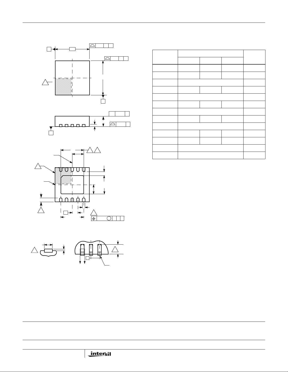
L10.3x3C
10 LEAD DUAL FLAT NO-LEAD PLASTIC PACKAGE
MILLIMETERS
SYMBOL
A 0.85 0.90 0.95 A1 - - 0.05 A3 0.20 REF -
b 0.20 0.25 0.30 5, 8
D 3.00 BSC D2 2.33 2.38 2.43 7, 8
C
E 3.00 BSC E2 1.59 1.64 1.69 7, 8
C
e 0.50 BSC k0.20- - L 0.35 0.40 0.45 8
N102
Nd 5 3
NOTES:
1. Dimensioning and tolerancing conform to ASME Y14.5-1994.
2. N is the number of terminals.
3. Nd refers to the number of terminals on D.
4. All dimensions are in millimeters. Angles are in degrees.
5. Dimension b applies to the metallized terminal and is measured
between 0.15mm and 0.30mm from the terminal tip.
6. The configuration of the pin #1 identifier is optional, but must be
located within the zone indicated. The pin #1 identi fier may be
either a mold or mark feature.
7. Dimensions D2 and E2 are for the exposed pads which provide
improved electrical and thermal performance.
8. Nominal dimensions are provided to assist with PCB Land
Pattern Design efforts, see Intersil Technical Brief TB389.
9. COMPLIANT TO JEDEC MO-229-WEED-3 except for
dimensions E2 & D2.
NOTESMIN NOMINAL MAX
Rev. 1 4/06
All Intersil U.S. products are manufactured, assembled and tested utilizing ISO9000 quality systems.
Intersil Corporation’s quality certifications can be viewed at www.intersil.com/design/quality
Intersil products are sold by description only. Intersil Corporation reserves the right to make changes in circuit design, software and/or specifications at any time without
notice. Accordingly, the reader is cautioned to verify that data sheets are current before placing orders. Information furnished by Intersil is believed to be accurate and
reliable. However, no responsibility is assumed by Intersil or its subsidiaries for its use; nor for any infringements of patents or other rights of third parties which may result
from its use. No license is granted by implic atio n or other wise u nde r any p a tent or patent rights of Intersil or its subsidiaries.
For information regarding Intersil Corporation and its products, see www.intersil.com
11
FN6437.1
March 7, 2008
 Loading...