

Page 1
®
ISL88731A
Data Sheet January 7, 2009
SMBus Level 2 Battery Charger
The ISL88731A is a highly integrated Lithium-ion battery
charger controller, programmab le over the SMBus system
management bus (SMBus). The ISL88731A is intended to be
used in a smart battery charger (SBC) within a smart battery
system (SBS) that throttles the charge power such that the
current from the AC-adapter is automatically limited. High
efficiency is achieved with a DC/DC synchronous-rectifier
buck converter, equipped with diode emulati on for enhanced
light load efficiency and system bus boosting prevention. The
ISL88731A charges one to four Lithium-ion series cells, and
delivers up to 8A charge current. Integrated MOSFET
drivers and bootstrap diode result in fewer components and
smaller implementation area. Low offset current-sense
amplifiers provide high accuracy with 10mΩ sense resistors.
The ISL88731A provides 0.5% end-of-charge battery
voltage accuracy.
The ISL88731A provides a digital output that indicates the
presence of the AC-adapter as well as an analog output
which indicates the adapter current within 4% accuracy.
The ISL88731A is available in a small 5mmx5mm 28 Ld thin
(0.8mm) QFN package. An evaluation kit is available to
reduce design time. The ISL88731A is available in Pb-Free
packages.
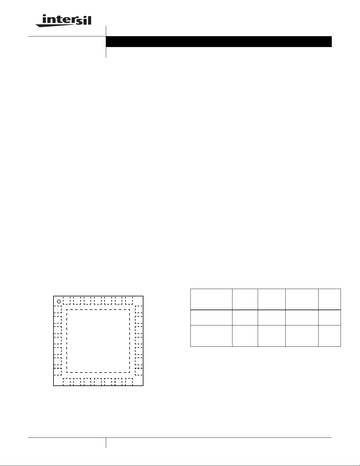
Pinout
ISL88731A
(28 LD TQFN)
TOP VIEW
CSSP
CSSN
VCC
BOOT
UGATE
PHASE
DCIN
28 27 26 25 24 23 22
NC
ACIN
VREF
ICOMP
NC
VCOMP
NC
1
2
3
4
5
6
7
8 9 10 11 12 13 14
ICM
SDA
SCL
VDDSMB
GND
ACOK
NC
21
20
19
18
17
16
15
VDDP
LGATE
PGND
CSOP
CSON
NC
VFB
FN6738.1
Features
• 0.5% Battery Voltage Accuracy
• 3% Adapter Current Limit Accuracy
• 3% Charge Current Accuracy
• SMBus 2 Wire Serial Interface
• Battery Short Circuit Protection
• Fast Response for Pulse-Charging
• Fast System-Load Transient Response
• Monitor Outputs
- Adapter Current (3% Accuracy)
- AC-Adapter Detection
• 11-Bit Battery Voltage Setting
• 6 Bit Charge Current/Adapter Current Setting
• 8A Maximum Battery Charger Current
• 11A Maximum Adapter Current
• +8V to +28V Adapter Voltage Range
• Pb-Free (RoHS compliant)
Applications
• Notebook Computers
• Tablet PCs
• Portable Equipment with Rechargeable Batteries
Ordering Information
PART
NUMBER
(Note)
ISL88731AHRZ ISL887
ISL88731AHRZ-T* ISL887
*Please refer to TB347 for details on reel specifications.
NOTE: These Intersil Pb-free plastic packaged products employ special
Pb-free material sets, molding compounds/die attach materials, and
100% matte tin plate plus anneal (e3 termination finish, which is RoHS
compliant and compatible with both SnPb and Pb-free soldering
operations). Intersil Pb-free products are MSL classified at Pb-free peak
reflow temperatures that meet or exceed the Pb-free requirements of
IPC/JEDEC J STD-020.
PART
MARKING
31AHRZ
31AHRZ
TEMP
RANGE
(°C)
-10 to +100 28 Ld 5x5
-10 to +100 28 Ld 5x5
PACKAGE
(Pb-Free)
TQFN
TQFN (Tape
and Reel)
PKG.
DWG. #
L28.5x5B
L28.5x5B
1
CAUTION: These devices are sensitive to electrostatic discharge; follow proper IC Handling Procedures.
1-888-INTERSIL or 1-888-468-3774
| Intersil (and design) is a registered trademark of Intersil Americas Inc.
Copyright Intersil Americas Inc. 2008, 2009. All Rights Reserved
All other trademarks mentioned are the property of their respective owners.
Page 2
ISL88731A
VDDSMB
SDA
SCL
CSSP
CSSN
IC O MP
CSOP
CSON
VFB
VCOMP
SMBUS
LEVEL
SHIFTER
20x
LEVEL
SHIFTER
20x
500k
11
6
6
100k
EN
DACS
DACI
DACV
DACS
DACI
EN
+
+
GMS
GMI
DACV
DACS
DACI
DACV
DCIN
LINEAR
REGU LATOR
+
GMV
-
BUFF
LVB
VDDP
CSO
LVB
VCC
REF
+
-
EN
DC/DC
CONVERTER
CSSP
REFERENCE
VREF
ACOK
ACIN
IC M
BOOT
UGATE
PHASE
VDDP
LGATE
PGND
GND
AC ADAPTER
AGND
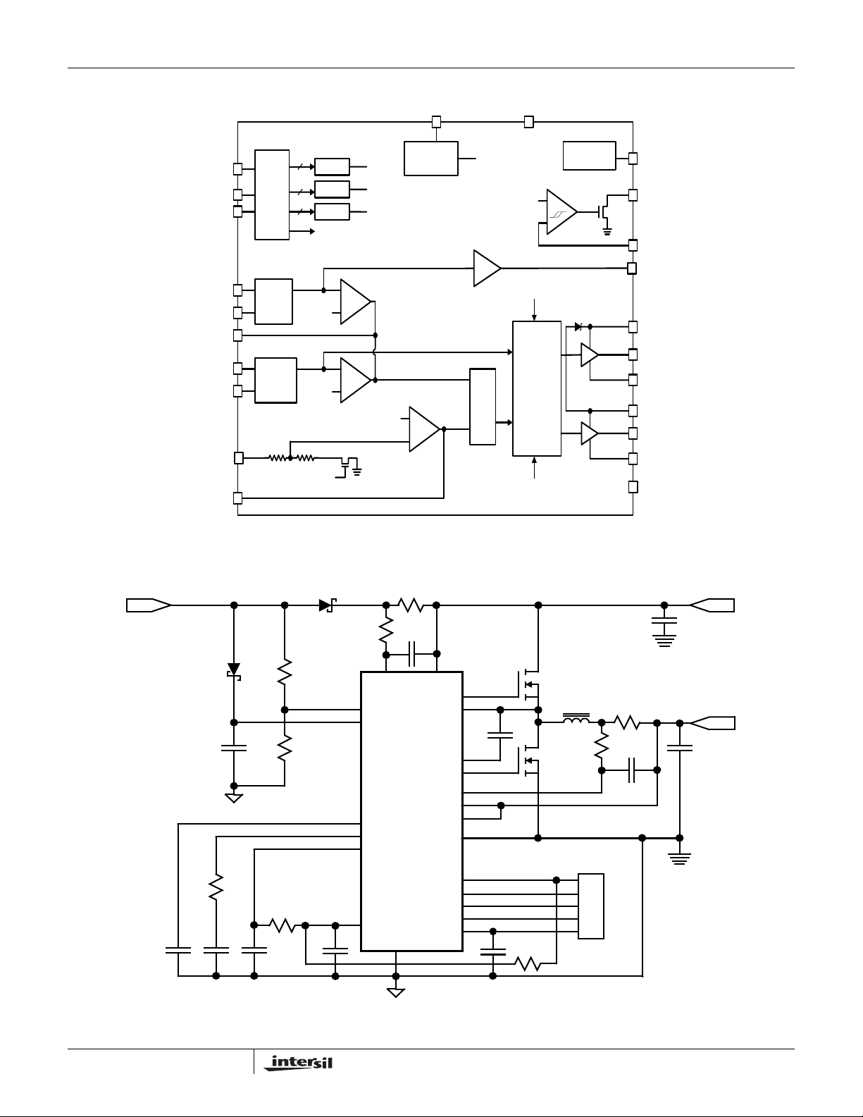
FIGURE 1. FUNCTIONAL BLOCK DIAGRAM
RS1
CSSNCSSP
UGATE
ACIN
DCIN
PHASE
ISL88731A
BOOT
LGATE
CSOP
CSON
ICOMP
VCOMP
VDDP
VREF
VCC
GND
VFB
PGND
ACOK
ICM
SDA
SCL
VDDSMB
TO SYSTEM
RS2
HOST
TO BATTERY
PGND
AGND
FIGURE 2. TYPICAL APPLICATION CIRCUIT
2
FN6738.1
January 7, 2009
Page 3
ISL88731A
Absolute Maximum Ratings
DCIN, CSSP, CSSN, CSOP, CSON, VFB . . . . . . . . . .-0.3V to +28V
CSSP-CSSN, CSOP-CSON, PGND-GND. . . . . . . . . -0.3V to +0.3V
PHASE to GND . . . . . . . . . . . . . . . . . . . . . . . . . . . . . . . -6V to +30V
BOOT to GND . . . . . . . . . . . . . . . . . . . . . . . . . . . . . . .-0.3V to +33V
BOOT to PHASE . . . . . . . . . . . . . . . . . . . . . . . . . . . . . .-0.3V to +6V
UGATE . . . . . . . . . . . . . . . . . . . . . . .PHASE - 0.3V to BOOT +0.3V
LGATE . . . . . . . . . . . . . . . . . . . . . . . .PGND - 0.3V to VDDP +0.3V
ICOMP, VCOMP, VREF, to GND . . . . . . . . . . . . -0.3V to VCC +0.3V
VDDSMB, SCL, SDA, ACIN, ACOK . . . . . . . . . . . . . . .-0.3V to +6V
VDDP, ICM, VCC to GND, VDDP to PGND. . . . . . . . . .-0.3V to +6V
CAUTION: Do not operate at or near the maximum ratings listed for extended periods of time. Exposure to such conditions may adversely impact product relia bility and
result in failures not covered by warranty.
NOTES:
is measured with the component mounted on a highly effective thermal conductivity test board on free air. See T ech Brief TB379 for det ails.
1. θ
JA
2. For θ
, the “case temp” location is the center of the exposed metal pad on the package underside.
JC
Thermal Information
Thermal Resistance (Typical, Notes 1, 2) θJA (°C/W) θJC (°C/W)
QFN Package. . . . . . . . . . . . . . . . . . . . 39 9.5
Junction Temperature Range. . . . . . . . . . . . . . . . . .-55°C to +150°C
Operating Temperature Range . . . . . . . . . . . . . . . .-10°C to +100°C
Storage Temperature . . . . . . . . . . . . . . . . . . . . . . . .-65°C to +150°C
Pb-Free Reflow Profile. . . . . . . . . . . . . . . . . . . . . . . . .see link below
http://www.intersil.com/pbfree/Pb-FreeReflow.asp
Electrical Specifications DCIN = CSSP = CSSN = 18V, CSOP = CSON = 12V, VDDP = 5V, BOOT-PHASE = 5.0V, GND = PGND = 0V,
CVDDP = 1µF, IVDDP = 0mA, T
at +25°C, unless otherwise specified. T emperature limits est ablished by characterization and are not production
tested.
PARAMETER CONDITIONS MIN TYP MAX UNITS
CHARGE VOLTAGE REGULATION
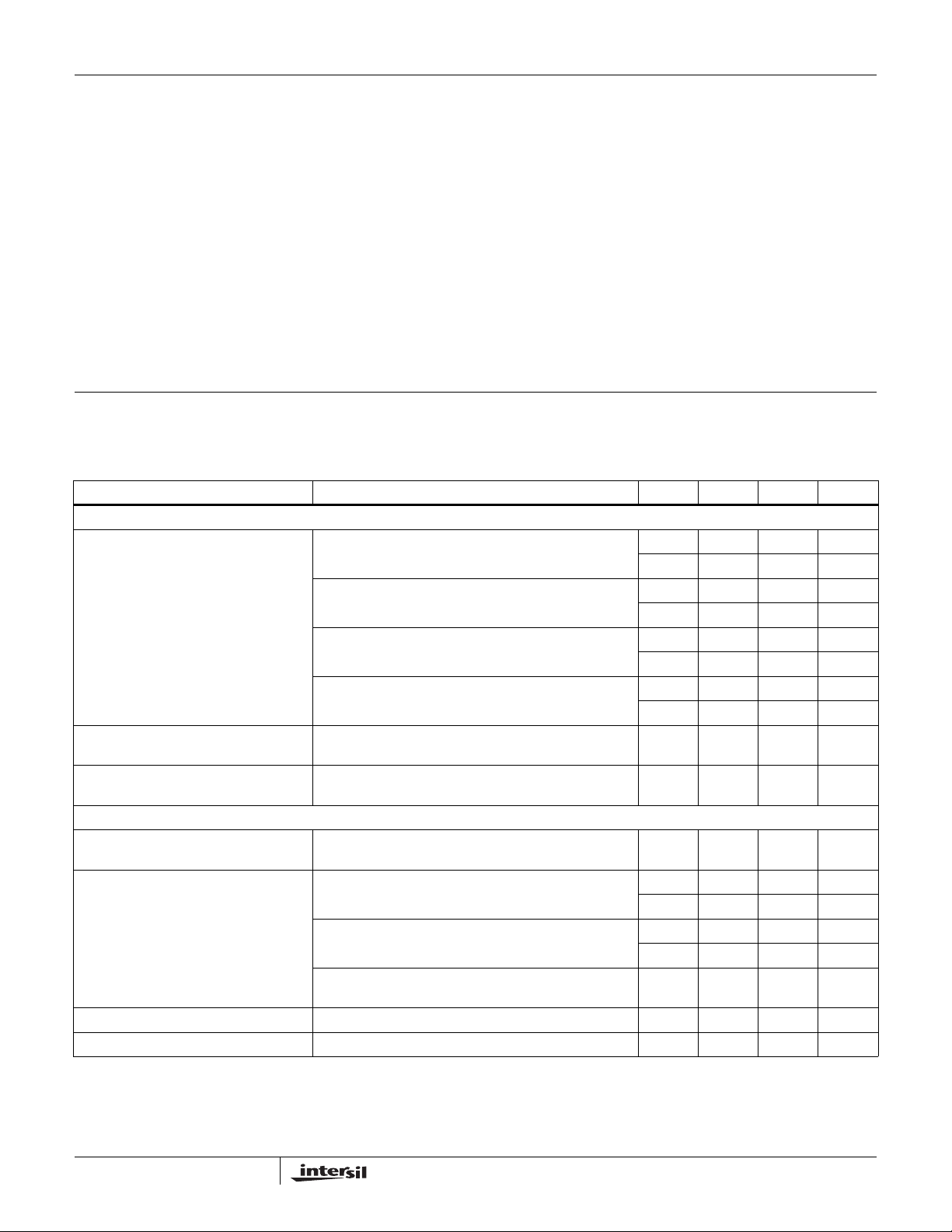
Battery Full Charge Voltage and Accuracy ChargeVoltage = 0x41A0 16.716 16.8 16.884 V
ChargeVoltage = 0x3130 12.529 12.592 12.655 V
ChargeVoltage = 0x20D0 8.350 8.4 8.450 V
ChargeVoltage = 0x1060 4.163 4.192 4.221 V
Battery Undervoltage Lockout Trip Point
for Trickle Charge
Battery Undervoltage Lockout Trip Point
Hysteresis
CHARGE CURRENT REGULATION
CSOP to CSON Full-Scale Current-Sense
Voltage
Charge Current and Accuracy RS2 = 10mΩ (see Figure 2)
Charge Current Gain Error Based on charge current = 128mA and 8.064A -1.6 1.4 %
CSOP/CSON Input Voltage Range 0 19 V
VFB rising 2.55 2.7 2.85 V
ChargingCurrent = 0x1f80
RS2 = 10mΩ (see Figure 2)
ChargingCurrent = 0x0f80
RS2 = 10mΩ (see Figure 2)
ChargingCurrent = 0x0080
= -10°C to +100°C. Parameters with MIN and/or MAX limits are 100% tested
A
-0.5 0.5 %
-0.5 0.5 %
-0.6 0.6 %
-0.7 0.7 %
100 250 400 mV
78.22 80.64 83.06 mV
7.822 8.064 8.306 A
-3 3 %
3.809 3.968 4.126 A
-4 4 %
64 128 220 mA
3
FN6738.1
January 7, 2009
Page 4
ISL88731A
Electrical Specifications DCIN = CSSP = CSSN = 18V, CSOP = CSON = 12V, VDDP = 5V, BOOT-PHASE = 5.0V, GND = PGND = 0V,
CVDDP = 1µF, IVDDP = 0mA, T
at +25°C, unless otherwise specified. T emperature limits est ablished by characterization and are not production
tested. (Continued)
PARAMETER CONDITIONS MIN TYP MAX UNITS
Battery Quiescent Current Adapter present, not charging,
I
CSOP
V
PHASE
+ I
CSON
= V
+ I
CSON
Adapter Absent
I
Adapter Quiescent Current I
+ I
CSOP
V
PHASE
DCIN+ICSSP+ICSSN
V
ADAPTER
+ I
CSON
= V
CSON
= 8V to 26V, V
INPUT CURRENT REGULATION
CSSP to CSSN Full-Scale Current-Sense
CSSP = 19V 106.7 110 113.3 mV
Voltage
Input Current Accuracy RS1 = 10mΩ (see Figure 2)
Adapter Current = 11004mA or 3584mA
RS1 = 10mΩ (see Figure 2)
Adapter Current = 2048mA
Input Current Limit Gain Error Based on InputCurrent = 1024mA and 11004mA -1.5 1.5 %
Input Current Limit Offset -1 1 mV
CSSP/CSSN Input Voltage Range 826V
ICM Gain V
CSSP-CSSN
ICM Offset Based on V
ICM Accuracy V
ICM Max Output Current V
CSSP-CSSN
V
CSSP-CSSN
V
CSSP-CSSN
CSSP-CSSN
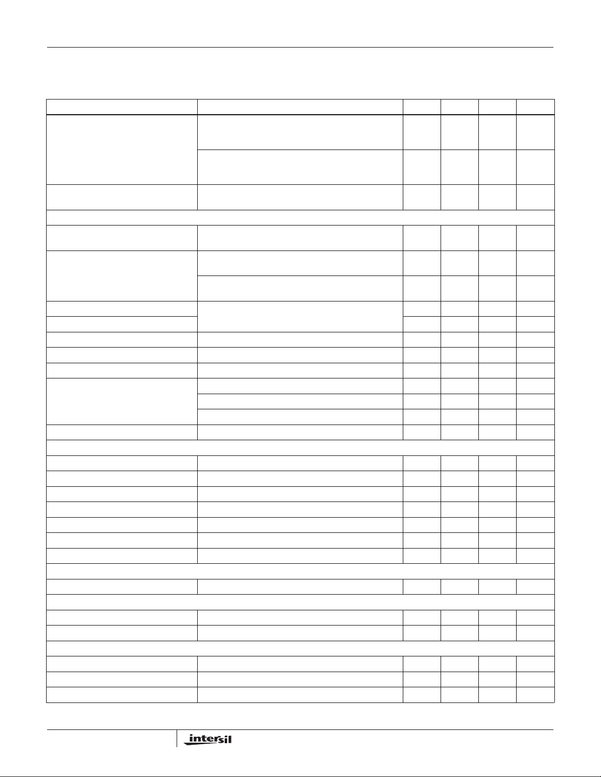
= 110mV 19.8 20 20.2 V/V
CSSP-CSSN
= 110mV -2.5 2.5 %
= 55mV or 35mV -4 4 %
= 20mV -8 8 %
= 0.1V 500 µA
SUPPLY AND LINEAR REGULATOR
DCIN, Input Voltage Range 826V
VDDP Output Voltage 8.0V < V
VDDP Load Regulation 0 < I
VDDP
< 28V, no load 4.9 5.1 5.3 V
DCIN
< 30mA 35 100 mV
VDDSMB Range 2.7 5.5 V
VDDSMB UVLO Rising 2.4 2.5 2.6 V
VDDSMB UVLO Hysteresis 100 150 200 mV
VDDSMB Quiescent Current VDDP = SCL = SDA = 5.5V 20 27 µA
V REFERENCE
VREF Output Voltage 0 < I
< 300µA 3.1 3.2 3.3 V
VREF
ACOK
ACOK Sink Current V
ACOK Leakage Current V
= 0.4V, ACIN = 1.5V 2 8 mA
ACOK
= 5.5V, ACIN = 2.5V 1 µA
ACOK
ACIN
ACIN rising Threshold 3.1 3.2 3.3 V
ACIN Threshold Hysteresis 40 60 90 mV
ACIN Input Bias Current -1 1 µA
= -10°C to +100°C. Parameters with MIN and/or MAX limits are 100% tested
A
135 400 µA
PHASE
= V
CSOP
+ I
CSSP
= V
+ I
DCIN
+ I
CSSN
= 19V, V
FB
ACIN
= 5V
-1 0.2 4 µA
PHASE
= V
CSOP
+ I
CSSP
= 19V, V
+ I
CSSN
DCIN
+ I
= 0V
FB
310mA
BATTERY
4V to 16.8V
-3 3 %
-5 5 %
= 110mV and 20mV -1.5 1.5 mV
4
FN6738.1
January 7, 2009
Page 5
ISL88731A
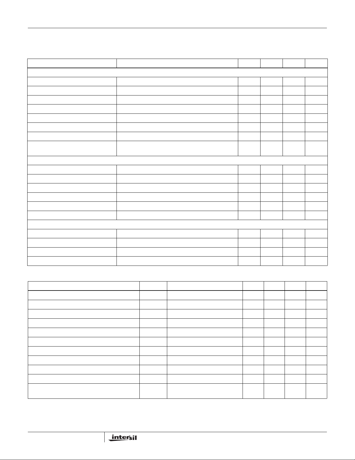
Electrical Specifications DCIN = CSSP = CSSN = 18V, CSOP = CSON = 12V, VDDP = 5V, BOOT-PHASE = 5.0V, GND = PGND = 0V,
CVDDP = 1µF, IVDDP = 0mA, T
at +25°C, unless otherwise specified. T emperature limits est ablished by characterization and are not production
tested. (Continued)
PARAMETER CONDITIONS MIN TYP MAX UNITS
SWITCHING REGULATOR
Frequency 330 400 440 kHz
BOOT Supply Current UGATE High 170 290 400 µA
PHASE Input Bias Current V
UGATE ON-Resistance Low I
UGATE ON-Resistance High I
LGATE ON-Resistance High I
LGATE ON-Resistance Low I
= 28V, V
DCON
= -100mA (Note 4) 0.9 1.6 Ω
UGATE
= 10mA (Note 4) 1.4 2.5 Ω
UGATE
= +10mA (Note 4) 1.4 2.5 Ω
LGATE
= -100mA (Note 4) 0.9 1.6 Ω
LGATE
Dead Time Falling UGATE to rising LGATE or
falling LGATE to rising UGATE
ERROR AMPLIFIERS
GMV Amplifier Transconductance 200 250 300 µA/V
GMI Amplifier Transconductance 40 50 60 µA/V
GMS Amplifier Transconductance 40 50 60 µA/V
GMI/GMS Saturation Current 15 21 25 µA
GMV Saturation Current 10 17 30 µA
ICOMP, VCOMP Clamp Voltage 0.25V < V
ICOMP, VCOMP
LOGIC LEVELS
SDA/SCL Input Low Voltage VDDSMB = 2.7V to 5.5V 0.8 V
SDA/SCL Input High Voltage VDDSMB = 2.7V to 5.5V 2 V
SDA/SCL Input Bias Current VDDSMB = 2.7V to 5.5V -1 1 µA
SDA, Output Sink Current V
= 0.4V 7 15 mA
SDA
= -10°C to +100°C. Parameters with MIN and/or MAX limits are 100% tested
A
CSON
= V
= 20V 0 2 µA
PHASE
35 50 80 ns
< 3.5V 200 300 400 mV
SMBus Timing Specification VDDSMB = 2.7V TO 5.5V
PARAMETERS SYMBOL CONDITIONS MIN TYP MAX UNITS
SMBus Frequency FSMB 10 100 kHz
Bus Free Time TBUF 4.7 µs
Start Condition Hold Time from SCL THD:STA 4 µs
Start Condition Setup Time from SCL TSU:STA 4.7 µs
Stop Condition Setup Time from SCL TSU:STO 4 µs
SDA Hold Time from SCL THD:DAT 300 ns
SDA Setup Time from SCL TSU:DAT 250 ns
SCL Low Timeout (Note 3) TTIMEOUT 22 25 30 ms
SCL Low Period TLOW 4.7 µs
SCL High Period THIGH 4 µs
Maximum Charging Period Without a SMBus Write to
ChargeVoltage or ChargeCurrent Register
NOTES:
3. If SCL is low for longer than the specified time, the charger is disabled.
4. Limits established by characterization and are not production tested.
5
140 180 220 s
FN6738.1
January 7, 2009
Page 6
ISL88731A
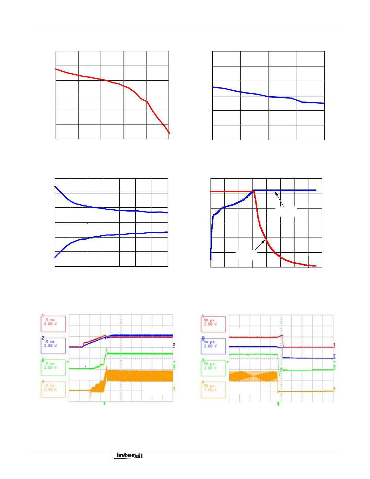
Typical Operating Performance DCIN = 20V, 3S2P Li-Battery, T
5.15
5.10
5.05
5.00
VDDP (V)
4.95
4.90
4.85
020406080100
VDDP LOAD CURRENT (mA)
FIGURE 3. VDD LOAD REGULATION
15
10
5
0
-5
ICM ACCURACY (%)
-10
3.23
3.22
3.21
3.20
VREF (V)
3.19
3.18
3.17
13.0
12.5
12.0
11.5
11.0
BATTERY VOLTAGE
10.5
= +25°C, unless otherwise noted.
A
0 50 100 150 200
I VREF (µA)
FIGURE 4. VREF LOAD REGULATION
VCHG (V)
ICHG (A)
1.0%
0.5%
0.0%
-0.5%
-1.0%
3.5
3.0
2.5
2.0
1.5
1.0
0.5
BATTERY CURRENT
-15
123 567
48
ADAPTER CURRENT (A)
FIGURE 5. ICM ACCURACY vs AC-ADAPTER CURRENT
VCOMP
ICOMP
CHARGE
CURRENT
INDUCTOR
CURRENT
FIGURE 7. CHARGE ENABLE
10.0
0 20406080100120140160
TIME (MINUTES)
0.0
FIGURE 6. TYPICAL CHARGING VOLTAGE AND CURRENT
ICOMP
VCOMP
CHARGE
CURRENT
INDUCTOR
CURRENT
FIGURE 8. CHARGE DISABLE
6
FN6738.1
January 7, 2009
Page 7
ISL88731A
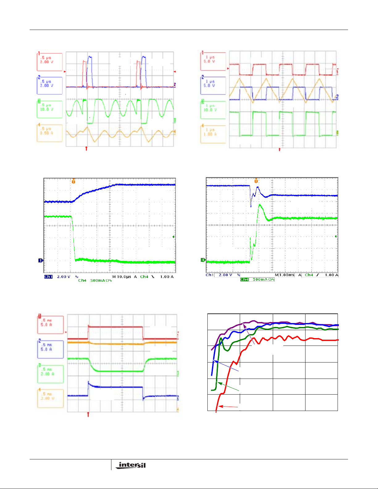
Typical Operating Performance DCIN = 20V, 3S2P Li-Battery, T
UGATE
PHASE
FIGURE 9. SWITCHING WAVEFORMS AT DIODE EMULATION
CSON/
V
BATTERY
LGATE
INDUCTOR
CURRENT
FIGURE 10. SWITCHING WAVEFORMS IN CC MODE
= +25°C, unless otherwise noted. (Continued)
A
UGATE
INDUCTOR
CURRENT
LGATE
PHASE
CSON/
V
BATTERY
BATTERY
CURRENT
FIGURE 11. BATTERY REMOVAL
SYSTEM
LOAD
BATTERY
VOLTAGE
CHARGE
CURRENT
ADAPTER
CURRENT
FIGURE 13. LOAD TRANSIENT RESPONSE
BATTERY
CURRENT
FIGURE 12. BATTERY INSERTION
100
95
90
85
80
75
70
04 8
16.8V
BATTERY
12.6V
BATTERY
8.4V
BATTERY
4.2V
BATTERY
26
CHARGE CURRENT (A)
FIGURE 14. EFFICIENCY vs CHARGE CURRENT AND
BATTERY VOLTAGE (EFFICIENCY DC
= 20V)
IN
7
FN6738.1
January 7, 2009
Page 8

ISL88731A
Functional Pin Descriptions
BOOT
High-Side Power MOSFET Driver Power-Supply
Connection. Connect a 0.1µF capacitor from BOOT to
PHASE.
UGATE
High-Side Power MOSFET Driver Output. Connect to the
high-side N-Channel MOSFET gate.
LGATE
Low-Side Power MOSFET Driver Output. Connect to
low-side N-Channel MOSFET. LGATE drives between
VDDP and PGND.
PHASE
High-Side Power MOSFET Driver Source Connection.
Connect to the source of the high-side N-Channel MOSFET.
CSOP
Charge Current-Sense Positive Input.
CSON
Charge Current-Sense Negative Input.
CSSP
Input Current-Sense Positive Input.
CSSN
Input Current-Sense Negative Input.
DCIN
Charger Bias Supply Input. Bypass DCIN with a 0.1µF
capacitor to GND.
ACIN
AC-adapter Detection Input. Connect to a resistor divider
from the AC-adapter output.
ACOK
AC Detect Output. This open drain output is high impedance
when ACIN is greater than 3.2V. The ACOK output remains
low when the ISL88731A is powered down. Connect a 10k
pull-up resistor from ACOK to VDDSMB.
ICM
Input Current Monitor Output. ICM voltage equals
20 x (V
CSSP
- V
CSSN
).
PGND
Power Ground. Connect PGND to the source of the low side
MOSFET.
VCC
Power input for internal analog circuits. Connect a 4.7Ω
resistor from VCC to VDDP and a 1µF ceramic capacitor
from VCC to ground.
VDDP
Linear Regulator Output. VDDP is the output of the 5.2V
linear regulator supplied from DCIN. VDDP also directly
supplies the LGATE driver and the BOOT strap diode.
Bypass with a 1µF ceramic capacitor from VDDP to PGND.
ICOMP
Compensation Point for the charging current and adapter
current regulation Loop. Connect 0.01µF to GND. See
“Voltage Control Loop” on page 20 for details of selecting the
ICOMP capacitor.
VCOMP
Compensation Point for the voltage regulation loop. Connect
4.7kΩ in series with 0.01µF to GND. See “Voltage Control
Loop” on page 20 for details on selecting VCOMP
components.
VFB
Feedback for the Battery Voltage.
VDDSMB
SMBus interface Supply Voltage Input. Bypass with a 0.1µF
capacitor to GND.
SDA
SMBus Data I/O. Open-drain Output. Connect an external
pull-up resistor according to SMBus specifications.
SCL
SMBus Clock Input. Connect an external pull-up resistor
according to SMBus specifications.
GND
Analog Ground. Connect directly to the backside paddle.
Connect to PGND close to the output capacitor.
Back Side Paddle
Connect the backside paddle to GND.
NC
No Connect. Pins 1, 5, 7 and 14 are not connected.
8
FN6738.1
January 7, 2009
Page 9

)
ISL88731A
Theory of Operation
Introduction
The ISL88731A includes all of the functions necessary to
charge 1-to-4 cell Li-ion and Li-polymer batteries. A high
efficiency synchronous buck converter is used to control the
charging voltage up to 19.2V and charging current up to 8A.
The ISL88731A also has input current limiting up to 11A. The
Input current limit, charge current limit and charge voltage
limit are set by internal registers written with SMBus.
Figure 2 shows the ISL88731A “Typica l Application Circuit”.
The ISL88731A charges the battery with constant charge
current, set by the ChargeCurrent register , until the battery
voltage rises to a voltage set by the ChargeVoltage register.
The charger will then operate at a constant voltage. The
adapter current is monitored and if the adapter current rises to
the limit set by the InputCurrent register, battery charge
current is reduced so the charger does not reduce the adapter
current available to the system.
The ISL88731A features a voltage regulation loop (VCOMP)
and two current regulation loops (ICOMP). The VCOMP
voltage regulation loop moni to rs VFB to limit the battery
charge voltage. The ICOMP current regulation loop limits the
battery charging current delivered to the battery to ensure
that it never exceeds the current set by the ChargeCurrent
register. The ICOMP current regulation loop also limits the
input current drawn from the AC-adapter to ensure that it
never exceeds the limit set by the InputCurrent register, and
to prevent a system crash and AC-adapter overload.
PWM Control
The ISL88731A employs a fixed frequency PWM control
architecture with a feed-forward function. The feed-forward
function maintains a constant modulator gain of 11 to achieve
fast line regulation as the input voltage changes.
The duty cycle of the buck regulator is controlled by the lower
of the voltages on ICOMP and VCOMP. The voltage on
ICOMP and VCOMP are inputs to a Lower V olt age Buf fer
(LVB) who ’ s output is the lo wer of the two inp ut s. The output
of the LVB is comp ared to an internal 400kHz ramp to produce
the Pulse Width Modulated signal that controls the UGATE
and LGA TE drivers. An internal clamp holds the highe r of the
two voltages (0.3V) above the lower voltage. This speeds the
transition from voltage loop control to current loop control or
vice versa.
The ISL88731A can operate up to 99.6% duty cycle if the
input voltage drops close to or below the battery charge
voltage (drop out mode). The DC/DC converter has a timer to
prevent the frequency from dropping into the audible
frequency range.
To prevent boosting of the system bus voltage, the battery
charger drives the lower FET in a way that prevents negative
inductor current.
An adaptive gate drive scheme is used to control the dead
time between two switches. The dead time control circuit
monitors the LGATE output and prevents the upper side
MOSFET from turning on until 20ns after LGATE falls below
1V V
, preventing cross-conduction and shoot-through.
GS
The same occurs for LGATE turn on. In order for the dead
time circuit to work properly, there must be a low resistance,
low inductance path from the LGATE driver to MOSFET
gate, and from the source of MOSFET to PGND. An internal
Schottky diode between the VDDP pin and BOOT pin keeps
the bootstrap capacitor charged.
AC-Adapter Detection
Connect the AC-adapter voltage through a resistor divider to
ACIN to detect when AC power is available, as shown in
Figure 2. ACOK is an ope n-drain output and is active low
when ACIN is less than V
above V
. The ACIN rising threshold is 3.2V (typ) with
th,rise
, and high when ACIN is
th,fall
57mV hysteresis.
Current Measurement
Use ICM to monitor the adapter current being sensed across
CSSP and CSSN. The output voltage range is 0V to 2.5V.
The voltage of ICM is proportional to the voltage drop across
CSSP and CSSN, and is given by Equation 1:
ICM 20 I
where I
⋅⋅=
INPUTRS1
ADAPTER
(EQ. 1
is the DC current drawn from the
AC-adapter. It is recommended to have an RC filter at the
ICM output for minimizing the switching noise.
VDDP Regulator
VDDP provides a 5.2V supply voltage from the internal LDO
regulator from DCIN and can deliver up to 30mA of
continuous current. The MOSFET drivers are powered by
VDDP. VDDP also supplies power to VCC through a
low-pass filter as shown in the “Typical Application Circuit”
(see Figure 2) on page 2. Bypass VDDP and VCC with a
1µF capacitor.
VDDSMB Supply
The VDDSMB input provides power to the SMBus interface.
Connect VDDSMB to VCC, or apply an external supply to
VDDSMB to keep the SMBus interface active while the
supply to DCIN is removed. When VDDSMB is biased the
internal registers are maintained. Bypass VDDSMB to GND
with a 0.1µF or greater ceramic capacitor.
Short Circuit Protection and 0V Battery Charging
Since the battery charger will regulate the charge current to
the limit set by the ChargeCurrent register, it automatically
has short circuit protection and is able to provide the charge
current to wake up an extremely discharged battery.
Undervoltage trickle charge folds back current if there is a
short circuit on the output.
9
FN6738.1
January 7, 2009
Page 10
ISL88731A
Undervoltage Detect and Battery Trickle Charging
If the voltage at CSON falls below 2.5V, the ISL88731A
reduces the charge current limit to 128mA to trickle charge
the battery. When the voltage rises above 2.7V the charge
current reverts to the programmed value in the
ChargeCurrent register.
Over-Temperature Protection
If the die temperature exceeds +150°C, it stops charging.
Once the die temperature drops below +125°C, charging will
start up again.
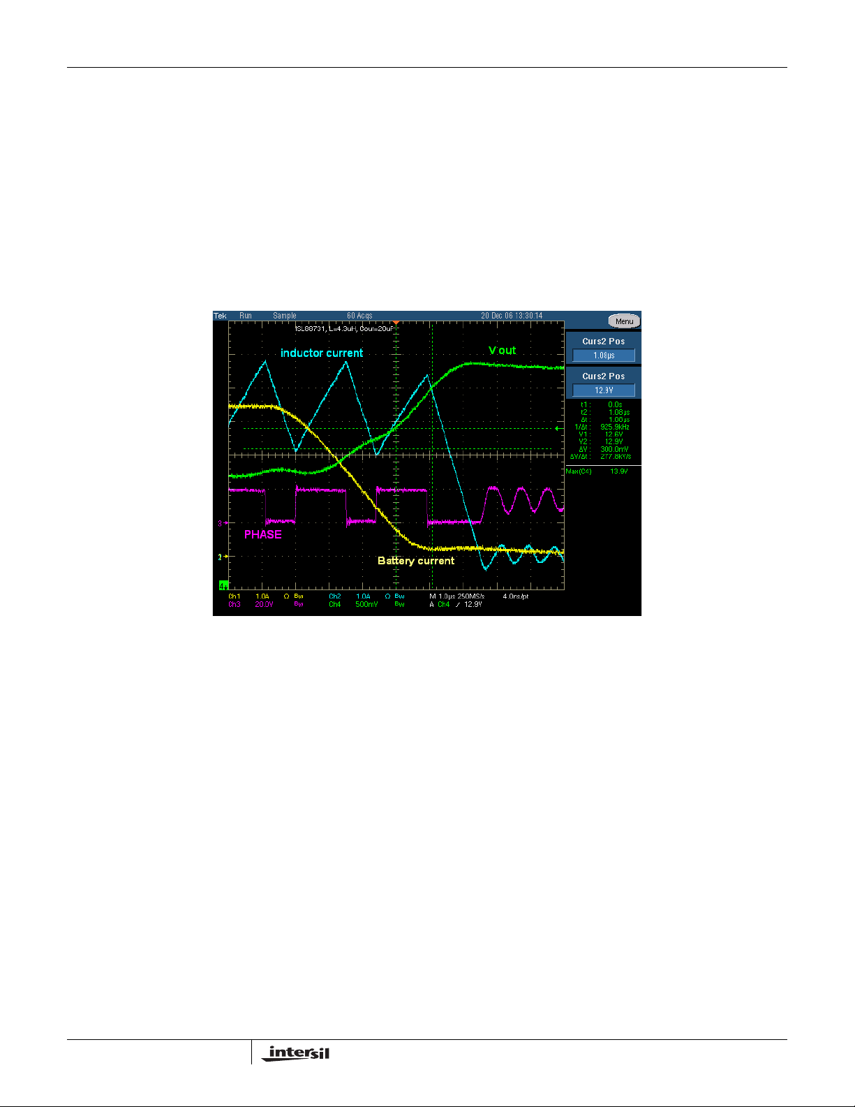
Overvoltage Protection
ISL88731 has an Overvoltage Protection circuit that limits
the output voltage when the battery is removed or
disconnected by a pulse charging circuit. If CSON exceeds
the output voltage set point in the chargevoltage register by
more than 300mV an internal comparator pulls VCOMP
down and turns off both upper and lower FET s of the buck as
in Figure 15. There is a delay of approximately 1µs between
V
exceeding the OVP trip point and pulling VCOMP,
OUT
LGATE and UGATE low. After UGATE and LGATE are
turned OFF inductor current continues to flow through the
body diode of the lower FET and V
inductor current reaches zero.
continues to rise until
OUT
FIGURE 15. OVERVOLTAGE PROTECTION IN ISL88731
10
FN6738.1
January 7, 2009
Page 11
ISL88731A
The System Management Bus
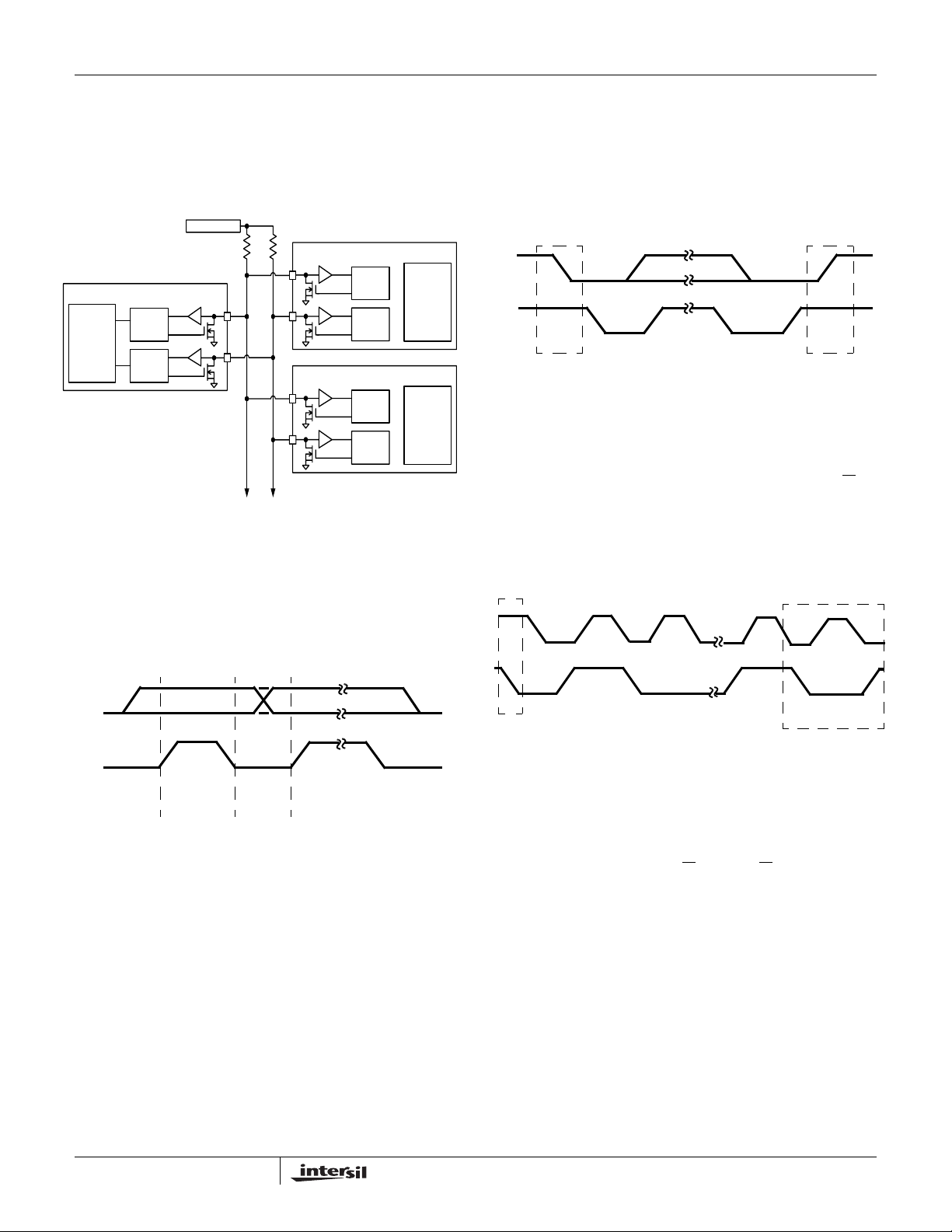
The System Management Bus (SMBus) is a 2-wire bus that
supports bidirectional communications. The protocol is
described briefly here. More detail is available from
www.smbus.org.
General SMBus Architecture
VDDSMB
SMBUS SLAVE
CPU
SMBUS MASTER
SCL
CONTROL
SDA
CONTROL
INPUT
OUTPUT
INPUT
OUTPUT
SCL
SDA
TO OTHER
SLAVE DEVICES
INPUT
OUTPUT
INPUT
OUTPUT
INP U T
OUTPUT
INP U T
OUTPUT
SCL
CONTROL
SDA
CONTROL
SMBUS SLAVE
SCL
CONTROL
SDA
CONTROL
STATE
MACHINE,
REGISTERS,
MEMORY,
ETC
STATE
MACHINE,
REGISTERS,
MEMORY,
ETC
Data Validity
The data on the SDA line must be stable during the HIGH
period of the SCL, unless generating a START or STOP
condition. The HIGH or LOW state of the data line can only
change when the clock signal on the SCL line is LOW. Refer
to Figure 16.
ST AR T and STOP Conditions
As shown in Figure 17, START condition is a HIGH-to-LOW
transition of the SDA line while SCL is HIGH.
The STOP condition is a LOW-to-HIGH transition on the SDA
line while SCL is HIGH. A STOP condition must be sent before
each STAR T condition.
SDA
SCL
SP
START
CONDITION
FIGURE 17. START AND STOP WAVEFORMS
STOP
CONDITION
Acknowledge
Each address and data transmission uses 9-clock pulses. The
ninth pulse is the acknowledge bit (ACK). After the start
condition, the master sends 7-slave address bits and a R/W
during the next 8-clock pulses. During the ninth clock pulse, the
device that recognizes its own address holds the data line low
to acknowledge. The acknowledge bit is also used by both the
master and the slave to acknowledge receipt of register
addresses and data (see Figure 18).
SCL
SDA
1
2
8
9
bit
SDA
SCL
DATA LINE
STABLE
DATA VALID
CHANGE
OF DATA
ALLOWED
FIGURE 16. DATA VALIDITY
MSB
START
ACKNOWLEDGE
FROM SLAVE
FIGURE 18. ACKNOWLEDGE ON THE I2C BUS
SMBus Transactions
All transactions start with a control byte sent from the SMBus
master device. The control byte begins with a Start condition,
followed by 7-bits of slave address (0001001 for the
ISL88731A) followed by the R/W
or 1 for a read. If any slave devices on the SMBus bus
recognize their address, they will Acknowledge by pulling the
serial data (SDA) line low for the last clock cycle in the control
byte. If no slaves exist at that address or are not ready to
communicate, the data line will be 1, indicating a Not
Acknowledge condition.
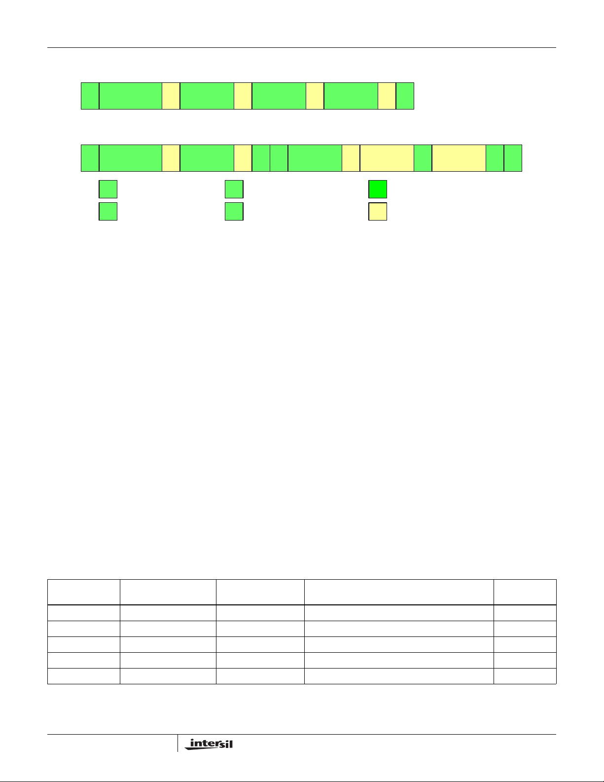
Once the control byte is sent, and the ISL88731A
acknowledges it, the 2nd byte sent by the master must be a
register address byte such as 0x14 for the ChargeCurrent
register. The register address byte tells the ISL88731A
which register the master will write or read. See Table 1 for
details of the registers. Once the ISL88731A receives a
register address byte it responds with an acknowledge.
bit. The R/W bit is 0 for a write
11
FN6738.1
January 7, 2009
Page 12
Write To A Register
ISL88731A
SLAVE
S A
ADDR + W
REGISTER
ADDR
LO BYTE
A A A
DATA
Read From A Register
SLAVE
S A P
ADDR + W
SSTART
PSTOP
REGISTER
ADDR
FIGURE 19. SMBus/ISL88731A READ AND WRITE PROTOCOL
A A NS A
P
ACKNOWLEDGE
A
NO ACKNOWLEDGE
N
Byte Format
Every byte put on the SDA line must be eight bits long and
must be followed by an acknowledge bit. Data is transferred
with the most significant bit first (MSB) and the least
significant bit last (LSB).
ISL88731A and SMBus
The ISL88731A receives control inputs from the SMBus
interface. The serial interface complies with the SMBus
protocols as documented in the System Management Bus
Specification V1.1, which can be downloaded from
www.smbus.org. The ISL88731A uses the SMBus
Read-Word and Write-Word protocols (Figure 19) to
communicate with the smart battery. The ISL88731A is an
SMBus slave device and does not initiate communication on
the bus. It responds to the 7-bit address 0b0001001_ (0x12).
Read address = 0b00010011 and
Write address = 0b00010010.
In addition, the ISL88731A has two identification (ID)
registers: a 16-bit device ID register and a 16-bit
manufacturer ID register.
SLAVE
ADDR + R
HI BYTE
DATA
LO BYTE
P
HI BYTE
DATA
DRIVEN BY THE MASTER
DRIVEN BY ISL88731
DATA
The data (SDA) and clock (SCL) pins have Schmitt-trigger
inputs that can accommodate slow edges. Choose pull-up
resistors for SDA and SCL to achieve rise times according to
the SMBus specifications. The ISL88731A is controlled by
the data written to the registers described in Table 1.
Battery Charger Registers
The ISL88731A supports five battery-charger registers that
use either Write-Word or Read-Word protocols, as
summarized in Table 1. ManufacturerID and DeviceID are
“read only” registers and can be used to identify the
ISL88731A. On the ISL88731A, ManufacturerID always
returns 0x0049 (ASCII code for “I” for Intersil) and DeviceID
always returns 0x0001.
Enabling and Disabling Charging
After applying power to ISL88731A, the internal registers
contain their POR values (see Table 1). The POR values for
charge current and charge voltage are 0x0000. These
values disable charging. To enable charging, the
ChargeCurrent register must be written with a number
>0x007F and the ChargeVoltage register must be written
with a number >0x000F . Charging can be disabled by writing
0x0000 to either of these registers.
TABLE 1. BATTERY CHARGER REGISTER SUMMARY
REGISTER
ADDRESS REGISTER NAME READ/WRITE DESCRIPTION POR STATE
0x14 ChargeCurrent Read or Write 6-bit Charge Current Setting 0x0000
0x15 ChargeVoltage Read or Write 11-bit Charge Voltage Setting 0x0000
0x3F InputCurrent Read or Write 6-bit Charge Current Setting 0x0080
0xFE ManufacturerID Read Only Manufacturer ID 0x0049
0xFF DeviceID Read Only Device ID 0x0001
12
FN6738.1
January 7, 2009
Page 13
ISL88731A
Setting Charge Voltage
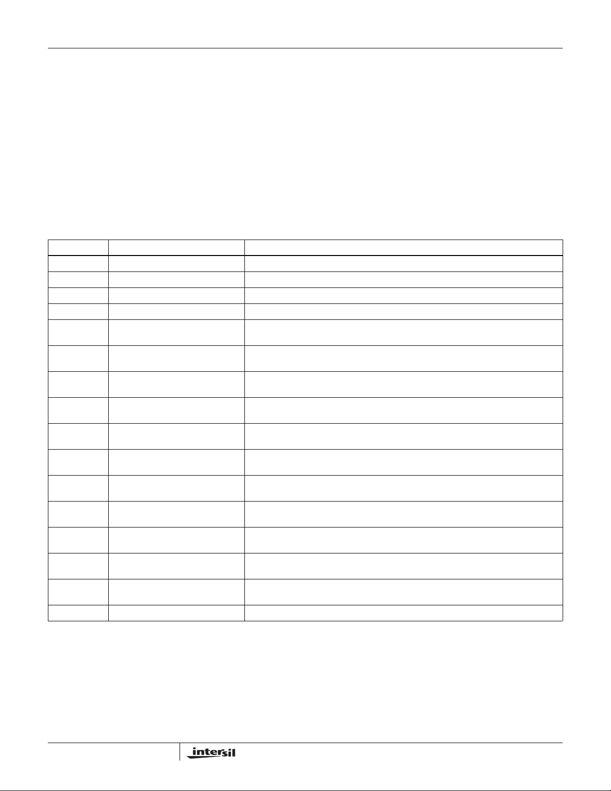
Charge voltage is set by writing a valid 16-bit number to the
ChargeVoltage register. This 16-bit number translates to a
65.535V full-scale voltage. The ISL88731A ignores the first 4
LSBs and uses the next 11 bits to set the voltage DAC. The
charge voltage range of the ISL88731A is 1.024V to
19.200V. Numbers requesting charge voltage greater than
19.200V result in a ChargeVoltage of 19.200V. All numbers
requesting charge voltage below 1.024V result in a voltage
set point of zero, which terminates charging. Upon initial
power-up or reset, the ChargeVoltage and ChargeCurrent
registers are reset to 0 and the charger remains shut down
ChargeCurrent registers. Use the Write-Word protocol
(Figure 19) to write to the ChargeVoltage register. The
register address for ChargeVoltage is 0x15. The 16-bit
binary number formed by D15–D0 represents the charge
voltage set point in mV. However, the resolution of the
ISL88731A is 16mV because the D0–D3 bits are ignored as
shown in Table 2. The D-5 bit is also ignored because it is
not needed to span the 1.024V to 19.2V range. Table 2
shows the mapping between the charge-voltage set point
and the 16-bit number written to the ChargeVoltage register.
The ChargeVoltage register can be read back to verify its
contents.
until valid numbers are sent to the ChargeVoltage and
TABLE 2. CHARGEVOLTAGE (REGISTER 0x15)
BIT BIT NAME DESCRIPTION
0 Not used
1 Not used
2 Not used
3 Not used
4 Charge Voltage, DACV 0 0 = Adds 0mV of charger voltage, 1024mV min
5 Charge Voltage, DACV 1 0 = Adds 0mV of charger voltage, 1024mV min
6 Charge Voltage, DACV 2 0 = Adds 0mV of charger voltage, 1024mV min
7 Charge Voltage, DACV 3 0 = Adds 0mV of charger voltage, 1024mV min
8 Charge Voltage, DACV 4 0 = Adds 0mV of charger voltage, 1024mV min
9 Charge Voltage, DACV 5 0 = Adds 0mV of charger voltage, 1024mV min
10 Charge Voltage, DACV 6 0 = Adds 0mA of charger voltage
11 Charge Voltage, DACV 7 0 = Adds 0mV of charger voltage
12 Charge Voltage, DACV 8 0 = Adds 0mV of charger voltage
13 Charge Voltage, DACV 9 0 = Adds 0mV of charger voltage
14 Charge Voltage, DACV 10 0 = Adds 0mV of charger voltage
15 Not used. Normally a 32768mV weight
1 = Adds 16mV of charger voltage
1 = Adds 32mV of charger voltage
1 = Adds 64mV of charger voltage
1 = Adds 128mV of charger voltage
1 = Adds 256mV of charger voltage
1 = Adds 512mV of charger voltage
1 = Adds 1024mV of charger voltage
1 = Adds 2048mV of charger voltage
1 = Adds 4096mV of charger voltage
1 = Adds 8192mV of charger voltage
1 = Adds 16384mV of charger voltage, 19200mV max
13
FN6738.1
January 7, 2009
Page 14
ISL88731A
Setting Charge Current
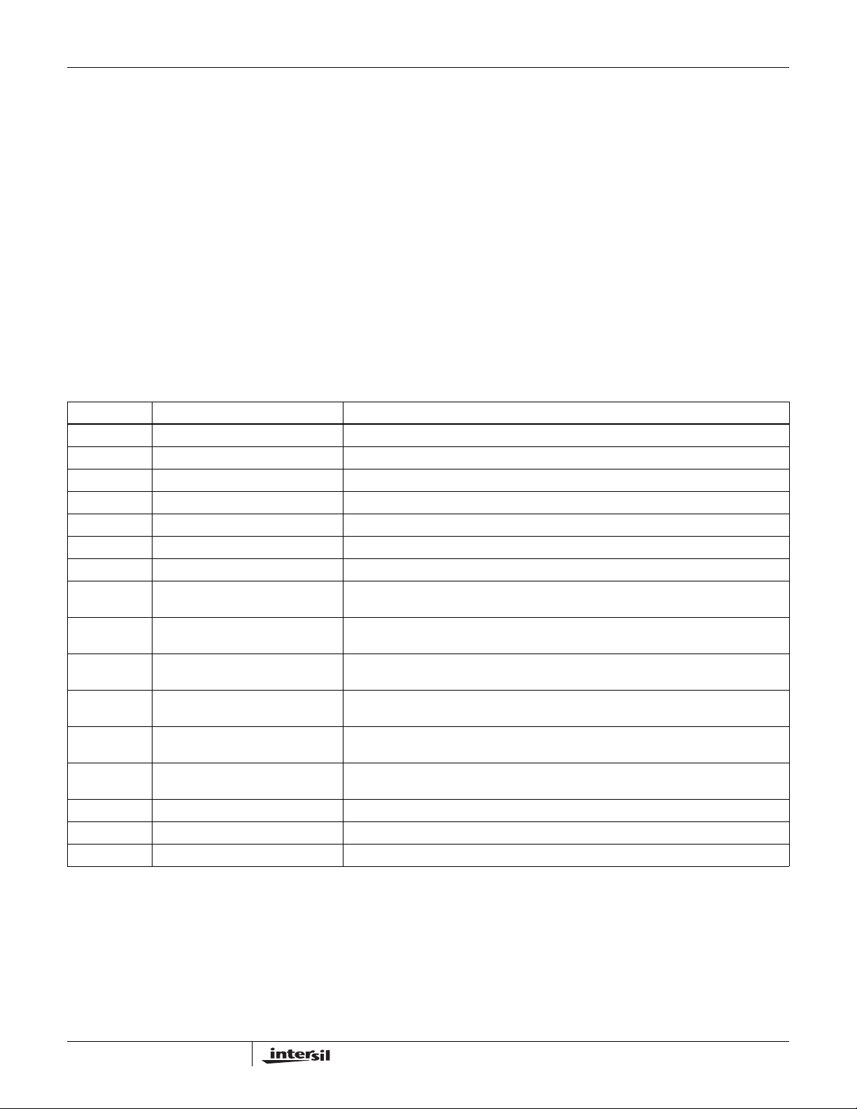
ISL88731A has a 16-bit ChargeCurrent register that sets the
battery charging current. ISL88731A controls the charge
current by controlling the CSOP-CSON voltage. The
register’s LSB translates to 10µV at CSON-CSOP. With a
10mΩ charge current R
LSB translates to 1mA charge current. The ISL88731A
ignores the first 7 LSBs and uses the next 6 bits to control
the current DAC. The charge-current range of the
ISL88731A is 0 to 8.064A (using a 10mΩ current-sense
resistor). All numbers requesting charge current above
8.064A result in a current setting of 8.064A. All numbers
requesting charge current between 0mA to 128mA result in
a current setting of 0mA. The default charge current setting
at Power-On Reset (POR) is 0mA. To stop charging, set
resistor (RS2 in Figure 2), the
sense
and the charger is disabled. To st art the charger, write valid
numbers to the ChargeVoltage and ChargeCurrent registers.
The ChargeCurrent register uses the Write-Word protocol
(see Figure 19). The register code for ChargeCurrent is 0x14
(0b00010100). Table 3 shows the mapping between the
charge current set point and the ChargeCurrent number. The
ChargeCurrent register can be read back to verify its
contents.
The ISL88731A includes a fault limiter for low battery
conditions. If the battery voltage is less than 2.5V , the charge
current is temporarily set to 128mA. The ChargeCurrent
register is preserved and becomes active again when the
battery voltage is higher than 2.7V. This function effectively
provides a foldback current limit, which protects the charger
during short circuit and overload.
ChargeCurrent to 0. Upon initial power-up, the
ChargeVoltage and ChargeCurrent registers are reset to 0
TABLE 3. CHARGE CURRENT (REGISTER 0x14) (10mΩ SENSE RESISTOR, RS2)
BIT BIT NAME DESCRIPTION
0 Not used
1 Not used
2 Not used
3 Not used
4 Not used
5 Not used
6 Not used
7 Charge Current, DACI 0 0 = Adds 0mA of charger current
1 = Adds 128mA of charger current
8 Charge Current, DACI 1 0 = Adds 0mA of charger current
1 = Adds 256mA of charger current
9 Charge Current, DACI 2 0 = Adds 0mA of charger current
10 Charge Current, DACI 3 0 = Adds 0mA of charger current
11 Charge Current, DACI 4 0 = Adds 0mA of charger current
12 Charge Current, DACI 5 0 = Adds 0mA of charger current
13 Not used
14 Not used
15 Not used
1 = Adds 512mA of charger current
1 = Adds 1024mA of charger current
1 = Adds 2048mA of charger current
1 = Adds 4096mA of charger current, 8064mA max
14
FN6738.1
January 7, 2009
Page 15
ISL88731A
Setting Input-Current Limit
The total power from an AC-adapter is the sum of the power
supplied to the system and the power into the charger and
battery. When the input current exceeds the set input current
limit, the ISL88731A decreases the charge current to provide
priority to system load current. As the system load rises, the
available charge current drops linearly to zero. Thereafter, the
total input current can increase to the limit of the AC-adapter.
The internal amplifier compares the differential voltage
between CSSP and CSSN to a scaled voltage set by the
InputCurrent register. The total input current is the sum of
the device supply current, the charger input current, and the
system load current. The total input current can be estimated
by using Equation 2.
I
INPUTISYSTEMICHARGEVBATTERY
Where η is the efficiency of the DC/DC converter (typically
85% to 95%).
The ISL88731A has a 16-bit InputCurrent register that
translates to a 2mA LSB and a 131.071A full-scale current
using a 10mΩ current-sense resistor (RS1 in Figure 2).
Equivalently, the 16-bit InputCurrent number sets the voltage
across CSSP and CSSN inputs in 20µV per LSB increments.
×()VINη×()⁄[]+=
(EQ. 2)
To set the input current limit use the SMBus to write a 16-bit
InputCurrent register using the data format listed in Table 4.
The InputCurrent register uses the Write-Word protocol (see
Figure 19). The register code for InputCurrent is 0x3F
(0b00111111). The InputCurrent register can be read back to
verify its contents.
The ISL88731A ignores the first 7 LSBs and uses the next
6 bits to control the input-current DAC. The input-current
range of the ISL88731A is from 256mA to 11.004A. All 16-bit
numbers requesting input current above 11.004A result in an
input-current setting of 11.004A. All 16-bit numbers
requesting input current between 0mA to 256mA result in an
input-current setting of 0mA. The default input-current-limit
setting at POR is 256mA. When choosing the current-sense
resistor RS1, carefully calculate its power rating. Take into
account variations in the system’s load current and the
overall accuracy of the sense amplifier. Note that the voltage
drop across RS1 contributes additiona l pow e r lo ss, wh i ch
reduces efficiency. System currents normally fluctuate as
portions of the system are powered up or put to sleep.
Without input current regulation, the input source must be
able to deliver the maximum system current and the
maximum charger-input current. By using the
input-current-limit circuit, the output-current capability of the
AC wall adapter can be lowered, reducing system cost.
TABLE 4. INPUT CURRENT (REGISTER 0x3F) (10mΩ SENSE RESISTOR, RS1)
BIT BIT NAME DESCRIPTION
0 Not used
1 Not used
2 Not used
3 Not used
4 Not used
5 Not used
6 Not used
7 Input Current, DACS 0 0 = Adds 0mA of input current
1 = Adds 256mA of input current
8 Input Current, DACS 1 0 = Adds 0mA of input current
1 = Adds 512mA of input current
9 Input Current, DACS 2 0 = Adds 0mA of input current
10 Input Current, DACS 3 0 = Adds 0mA of input current
11 Input Current, DACS 4 0 = Adds 0mA of input current
12 Input Current, DACS 5 0 = Adds 0mA of input current
13 Not used
14 Not used
15 Not used
1 = Adds 1024mA of input current
1 = Adds 2048mA of input current
1 = Adds 4096mA of input current
1 = Adds 8192mA of input current, 11004mA max
15
FN6738.1
January 7, 2009
Page 16

ISL88731A
Charger Timeout
The ISL88731A includes 2 timers to insure the SMBus
master is active and to prevent overcharging the battery.
ISL88731A will terminate charging if the charger has not
received a write to the ChargeVoltage or ChargeCurrent
register within 175s or if the SCL line is low for more than
25ms. If a time-out occurs, either ChargeVoltage or
ChargeCurrent registers must be written to re-enable
charging.
ISL88731A Data Byte Order
Each register in ISL88731A contains 16bits or 2, 8 bit bytes.
All data sent on the SMBus is in 8-bit bytes and 2 bytes must
be written or read from each register in ISL88731A. The
order in which these bytes are transmitted appears reversed
from the way they are normally written. The LOW byte is
sent first and the HI byte is sent second. For example, When
writing 0x41A0, 0xA0 is written first and 0x41 is sent second.
Writing to the Internal Registers
In order to set the charge current, charge voltage or input
current, valid 16-bit numbers must be written to ISL88731A’s
internal registers via the SMBus.
To write to a register in the ISL88731A, the master sends a
control byte with the R/W
bit set to 0, indicating a write. If it
receives an Acknowledge from the ISL88731A it sends a
register address byte setting the register to be written (i.e.
0x14 for the ChargeCurrent register). The ISL88731A will
respond with an Acknowledge. The master then sends the
lower data byte to be written into the desired register. The
ISL88731A will respond with an Acknowledge. The master
then sends the higher data byte to be written into the desired
register. The ISL88731A will respond with an Acknowledge.
The master then issues a Stop condition, indicating to the
ISL88731A that the current transaction is complete. Once
this transaction completes, the ISL88731A will begin
operating at the new current or voltage.
ISL88731A does not support writing more than one register
per transaction.
Reading from the Internal Registers
The ISL88731A has the ability to read from 5 internal
registers. Prior to reading from an internal register , the master
must first select the desired register by writing to it and
sending the registers address byte. This process begins by
the master sending a control byte with the R/W
indicating a write. Once it receives an Acknowledge from the
ISL88731A it sends a register address byte representing the
internal register it wants to read. The ISL88731A will respond
with an Acknowledge. The master must then respond with a
Stop condition. Af ter the Stop condition, the master follows
with a new St art condition, then sends a new control byte with
the ISL88731A slave address and the R/W
indicating a read. The ISL88731A will Acknowledge then send
bit set to 0,
bit set to 1,
the lower byte stored in that register. Af ter re ce iving the byte,
the master Acknowledges by holding SDA low during the 9th
clock pulse. ISL88731A then sends the higher byte stored in
the register. After the seco nd byte, neither device hold s SDA
low (No Acknowledge). The master will then produce a Stop
condition to end the read transaction.
ISL88731A does not support reading more than 1 register
per transaction.
Application Information
The following battery charger design refers to the ”Typical
Application Circuit” (see Figure 2) on page2, where typical
battery configuration of 3S2P is used. This section describes
how to select the external components including the
inductor, input and output capacitors, switching MOSFETs
and current sensing resistors.
Inductor Selection
The inductor selection has trade-offs between cost, size,
crossover frequency and efficiency. For example, the lower
the inductance, the smaller the size, but ripple current is
higher. This also results in higher AC losses in the magnetic
core and the windings, which decreases the system
efficiency. On the other hand, the higher inductance results
in lower ripple current and smaller output filter capacitors,
but it has higher DCR (DC resistance of the inductor) loss,
lower saturation current and has slower transient response.
So, the practical inductor design is based on the inductor
ripple current being ±15% to ±20% of the maximum
operating DC current at maximum input voltage. Maximum
ripple is at 50% duty cycle or V
BAT=VIN,MAX
required inductance for ±15% ripple current can be
calculated from Equation 3:
V
IN MAX,
---------------------------------------------------------
L
=
4FSW0.3 I⋅
⋅⋅
Where, V
IN,(MAX)
switching frequency and I
LMAX,
is the maximum input voltage, FSW is the
is the max DC current in
L,(MAX)
the inductor.
For V
IN,(MAX)
f
= 400kHz, the calcul ated inductance is 9.3µH. Choosing
s
= 20V, V
= 12.6V, I
BAT
BAT,(MAX)
the closest standard value gives L = 10µH. Ferrite cores are
often the best choice since they are optimized at 400kHz to
600kHz operation with low core loss. The core must be large
enough not to saturate at the peak inductor current I
Equation 4:
1
I
PEAKILMAX,
-- -
+ I
2
⋅=
RIPPLE
Inductor saturation can lead to cascade failures due to very
high currents. Conservative design limits the peak and RMS
current in the inductor to less than 90% of the rated
saturation current.
Crossover frequency is heavily dependent on the inductor
value. F
should be less than 20% of the switching
CO
/2. The
(EQ. 3)
= 4.5A, and
Peak
(EQ. 4)
in
16
FN6738.1
January 7, 2009
Page 17

ISL88731A
frequency and a conservative design has FCO less than
10% of the switching frequency. The highest F
CO
is in
voltage control mode with the battery removed and may be
calculated (approximately) from Equation 5:
511R
⋅⋅
F
CO
------------------------------------------ -
=
2π L⋅
SENSE
(EQ. 5)
Output Capacitor Selection
The output capacitor in parallel with the battery is used to
absorb the high frequency switching ripple current and
smooth the output voltage. The RMS value of the output
ripple current I
V
RMS
-----------------------------------
12LF
I
is given by Equation 6:
RMS
IN MAX,
⋅⋅
D1D–()⋅⋅=
SW
(EQ. 6)
Where the duty cycle D is the ratio of the output voltage
(battery voltage) over the input voltage for continuous
conduction mode which is typical operation for the battery
charger . During t he batter y charge pe riod, the output vol tage
varies from its initial battery voltage to the rated battery
voltage. So, the duty cycle varies from 0.53 for the minimum
battery voltage of 7.5V (2.5V/Cell) to 0.88 for the maximum
battery voltage of 12.6V. The maximum RMS value of the
output ripple current occurs at the duty cycle of 0.5 and is
expressed as Equation 7:
V
IN MAX,
I
For V
f
s
-------------------------------------------
=
RMS
4 12LF
⋅⋅⋅
IN,(MAX)
SW
= 19V, V
= 16.8V, L = 10µH, and
BAT
(EQ. 7)
= 400kHz, the maximum RMS current is 0.19A. A typical
20µF ceramic capacitor is a good choice to absorb this
current and also has very small size. Organic polymer
capacitors have high capacitance with small size and have a
significant equivalent series resistance (ESR). Although
ESR adds to ripple voltage, it also creates a high frequency
zero that helps the closed loop operation of the buck
regulator.
EMI considerations usually make it desirable to minimize
ripple current in the battery leads. Beads may be added in
series with the battery pack to increase the battery
impedance at 400kHz switching frequency. Switching ripple
current splits between the battery and the output capacitor
depending on the ESR of the output capacitor and battery
impedance. If the ESR of the output capacitor is 10mΩ and
battery impedance is raised to 2Ω with a bead, then only
0.5% of the ripple current will flow in the battery.
MOSFET Selection
The Notebook battery charger synchronous buck converter
has the input voltage from the AC-adapter output. The
maximum AC-adapter output voltage does not exceed 25V.
Therefore, 30V logic MOSFET should be used.
The high-side MOSFET must be able to dissipate the
conduction losses plus the switching losses. For the battery
charger application, the input voltage of the synchronous
buck converter is equal to the AC-adapter output voltage,
which is relatively constant. The maximum efficiency is
achieved by selecting a high-side MOSFET that has the
conduction losses equal to the switching losses. Switching
losses in the low-side FET are very small. The choice of
low-side FET is a trade-off between conduction losses
(r
the low-side FET is 2x the r
) and cost. A good rule of thumb for the r
DS(ON)
DS(ON)
of the high-side FET.
DS(ON)
of
The LGATE gate driver can drive sufficient gate current to
switch most MOSFETs efficiently. However , some FETs may
exhibit cross conduction (or shoot-through) due to current
injected into the drain-to-source parasitic capacitor (C
gd
) by
the high dV/dt rising edge at the phase node when the
high-side MOSFET turns on. Although LGATE sink current
(1.8A typical) is more than enough to switch the FET off
quickly, voltage drops across parasitic impedances between
LGATE and the MOSFET can allow the gate to rise during
the fast rising edge of voltage on the drain. MOSFETs with
low threshold voltage (<1.5V) and low ratio of C
gs/Cgd
(<5)
and high gate resistance (>4Ω) may be turned on for a few
ns by the high dV/dt (rising edge) on their drain. This can be
avoided with higher threshold voltage and C
gs/Cgd
ratio.
Another way to avoid cross conduction is slowing the turn-on
speed of the high-side MOSFET by connecting a resistor
between the BOOT pin and the boot strap capacitor.
For the high-side MOSFET, the worst-case conduction
losses occur at the minimum input voltage, as shown in
Equation 8:
V
OUT
P
Q1 conduction,
--------------- -
V
IN
⋅⋅=
I
BAT
2
r
DS ON()
(EQ. 8)
The optimum efficiency occurs when the switching losses
equal the conduction losses. However, it is difficult to
calculate the switching losses in the high-side MOSFET
since it must allow for difficult-to-quantify factors that
influence the turn-on and turn-off times. These factors
include the MOSFET internal gate resistance, gate charge,
threshold voltage, stray inductance and the pull-up and pulldown resistance of the gate driver.
The following switching loss calculation (Equation 9)
provides a rough estimate.
P
Q1 Switching,
1
-- -
V
INILVfsw
2
=
Q
⎛⎞
gd
------------------------ -
⎜⎟
I
⎝⎠
gsource,
1
-- -
V
INILPfsw
2
Q
⎛⎞
gd
-----------------
++
⎜⎟
I
⎝⎠
gksin,
Q
rrVINfsw
(EQ. 9)
Where, the following are the peak gate-drive source/sink
current of Q
•Q
gd
•Q
rr
, respectively:
1
: drain-to-gate charge,
: total reverse recovery charge of the body-diode in
low-side MOSFET,
: inductor valley current,
•I
LV
: Inductor peak current,
•I
LP
•I
g,sink
•Ig,
source
17
FN6738.1
January 7, 2009
Page 18

ISL88731A
Low switching loss requires low drain-to-gate charge Qgd.
Generally, the lower the drain-to-gate charge, the higher the
ON-resistance. Therefore, there is a trade-off between the
ON-resistance and drain-to-gate charge. Good MOSFET
selection is based on the Figure of Merit (FOM), which is a
product of the total gate charge and ON-resistance. Usually,
the smaller the value of FOM, the higher the efficiency for
the same application.
For the low-side MOSFET, the worst-case power dissipation
occurs at minimum battery voltage and maximum input
voltage (Equation 10):
V
⎛⎞
P
1
–
⎜⎟
Q2
⎝⎠
OUT
--------------- -
V
IN
⋅⋅=
I
BAT
2
r
DS ON()
(EQ. 10)
Choose a low-side MOSFET that has the lowest possible
ON-resistance with a moderate-sized package like the SO-8
and is reasonably priced. The switching losses are not an
issue for the low-side MOSFET because it operates at
zero-voltage-switching.
Ensure that the required total gate drive current for the
selected MOSFETs should be less than 24mA. So, the to tal
gate charge for the high-side and low-side MOSFETs is
limited by Equation 11:
I
GATE
GATE
-----------------
≤
f
sw
is the total gate drive current and should be
GATE
= 24mA and fs= 400kHz
GATE
(EQ. 11)
Q
Where I
less than 24mA. Substituting I
into Equation 11 yields that the total gate charge should be
less than 80nC. Therefore, the ISL88731A easily drives the
battery charge current up to 8A.
Snubber Design
ISL88731A's buck regulator operates in discontinuous
current mode (DCM) when the load current is less than half
the peak-to-peak current in the inductor. After the low-side
FET turns off, the phase voltage rings due to the high
impedance with both FET s of f. This can be seen in Figure 9.
Adding a snubber (resistor in series with a capacitor) from
the phase node to ground can greatly reduce the ringing. In
some situations a snubber can improve output ripple and
regulation.
The snubber capacitor should be approximately twice the
parasitic capacitance on the phase node. This can be
estimated by operating at very low load current (100mA) and
measuring the ringing frequency.
C
SNUB
and 13:
C
SNUB
and R
-------------------------------------
=
2π F
()2L⋅
can be calculated from Equations 12
SNUB
2
ring
(EQ. 12)
R
SNUB
2L⋅
--------------------=
C
SNUB
(EQ. 13)
Input Capacitor Selection
The input capacitor absorbs the ripple current from the
synchronous buck converter, which is given by Equation 14:
()
−
VVV
=
I
BATrms
OUTINOUT
V
IN
(EQ. 14)
This RMS ripple current must be smaller than the rated RMS
current in the capacitor datasheet. Non-tantalum chemistries
(ceramic, aluminum, or OSCON) are preferred due to their
resistance to power-up surge currents when the AC-adapter
is plugged into the battery charger. For Notebook battery
charger applications, it is recommended that ceramic
capacitors or polymer capacitors from Sanyo be used due to
their small size and reasonable cost.
Loop Compensation Design
ISL88731A has three closed loop control modes. One
controls the output voltage when the battery is fully charged
or absent. A second controls the current into the battery
when charging and the third limits current drawn from the
adapter. The charge current and input current control loops
are compensated by a single capacitor on the ICOMP pin.
The voltage control loop is compensated by a network on the
VCOMP pin. Descriptions of these control loops and
guidelines for selecting compensation components will be
given in the following sections. Which loop controls the
output is determined by the minimum current buffer and the
minimum voltage buffer shown in the “Functional Block
Diagram” (see Figure 1) on page 2. These three loops will be
described separately.
Transconductance Amplifiers GMV, GMI and GMS
ISL88731A uses several transconductance amplifiers (also
known as gm amps). Most commercially available op amps
are voltage controlled voltage sources with gain expressed
as A = V
OUT/VIN
sources with gain expressed as gm = I
appear in some of the equations for poles and zeros in the
compensation.
PWM Gain F
The Pulse Width Modulator in the ISL88731A converts
voltage at VCOMP to a duty cycle by comparing VCOMP to
a triangle wave (duty = VCOMP/V
filter formed by L and C
output voltage (Vo = V
wave amplitude is proportional to V
amplitude proportional to DCIN makes the gain from
VCOMP to the PHASE output a constant 11 and is
independent of DCIN. For small signal AC analysis, the
battery is modeled by its internal resistance. The total output
resistance is the sum of the sense resistor and the internal
resistance of the MOSFETs, inductor and capacitor.
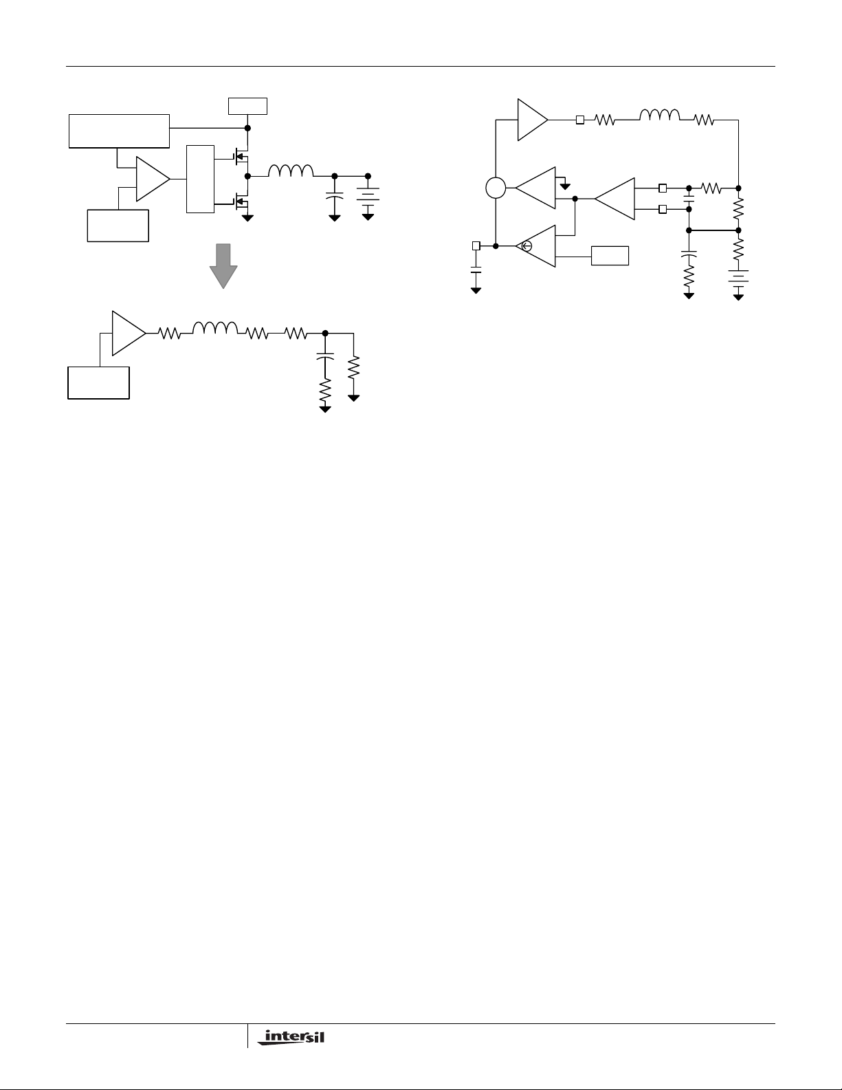
Figure20 shows the small signal model of the pulse width
modulator (PWM), power stage, output filter and battery.
. gm amps are voltage controlled current
OUT/VIN
. gm will
m
convert the duty cycle to a DC
O
DCIN
P-P RAMP
*duty). In ISL88731A, the triangle
DCIN
). The low-pass
. Making the ramp
18
FN6738.1
January 7, 2009
Page 19
A
ISL88731A
VDD
RAMP GEN
= VDD/11
V
RAMP
L
-
+
PWM
INPUT
PWM
GAIN=11
11
R
FET_RDSON
PWM
INPUT
FIGURE 20. SMALL SIGNAL AC MODEL
In most cases the Battery resistance is very small (<200mΩ)
resulting in a very low Q in the output filter. This results in a
frequency response from the input of the PWM to the
inductor current with a single pole at the frequency
calculated in Equation 15:
R
SENSErDS ON()RDCRRBAT
F
POLE1
------------------------------------------------------------------------------------------------------ -
=
The output capacitor creates a pole at a very high frequency
due to the small resistance in parallel with it. The frequency
of this pole is calculated in Equation 16:
DRIVERS
L
R
L_DCR
R
R
C
O
SENSE
C
O
ESR
R
BAT
+++()
2π L⋅
(EQ. 15)
+
+
-
-
L
L
CSOP
CSOP
CSON
CSON
R
R
L_DCR
L_DCR
C
C
F2
F2
C
O
C
O
R
ESR
R
ESR
R
R
F2
F2
R
R
S2
S2
R
BAT
R
BAT
ICOMP
ICOM P
Σ
S
S
Σ
C
C
ICOMP
ICOMP
11
11
0.25
0.25
GMI
GMI
PHASE
PHASE
+
+
-
-
-
-
+
+
R
R
FET_RDSON
FET_RDSON
CA2
CA2
DACI
DACI
20X
20X
FIGURE 21. CHARGE CURRENT LIMIT LOOP
frequency (smaller C
), the DC gain will be higher but
ICOMP
the phase margin will be lower. Use a capacitor on ICOMP
that is equal to or greater than the value calculated in
Equation 18. The factor of 1.5 is to ensure the zero is at a
frequency lower than the pole including tolerance variations.
C
ICOMP
------------------------------------------------------------------------------------------------------ -
=
A filter should be added between R
1.5 4 50μAV⁄()L⋅⋅ ⋅
R
+++()
SENSErDS ON()RDCRRBAT
and CSOP and CSON
S2
(EQ. 18)
to reduce switching noise. The filter roll-off frequency should
be between the crossover frequency and the switching
frequency (~100kHz). R
should be small (<10Ω) to
F2
minimize offsets due to leakage current into CSOP. The filter
cut off frequency is calculated using Equation 19:
1
-------------------------------------------
F
FILTER
=
⋅⋅()
2π C
F2RF2
(EQ. 19)
F
POLE2
1
---------------------------------------
=
⋅⋅
2π C
oRBAT
(EQ. 16)
The crossover frequency is determined by the DC gain of the
modulator and output filter and the pole in Equation 16. The
DC gain is calculated in Equation 20 and the crossover
Charge Current Control Loop
When the battery is less than the fully charged, the voltage
error amplifier goes to it’s maximum output (limited to 0.3V
above ICOMP) and the ICOMP voltage controls the loop
through the minimum voltage buffer. Figure 22 shows the
charge current control loop.
The compensation capacitor (C
) gives the error
ICOMP
amplifier (GMI) a pole at a very low frequency (<<1Hz) and a
a zero at F
. F
is created by the 0.25*CA2 output added to
Z1
Z1
ICOMP. The frequency can be calculated from Equation 17:
frequency is calculated with Equation 21:
11 R⋅
------------------------------------------------------------------------------------------------------ -
=
DC
R
SENSErDS ON()RDCRRBAT
⋅
==
F
COADCFPOLE
SENSE
+++()
11 R⋅
SENSE
---------------------------------- -
2π L⋅
(EQ. 20)
(EQ. 21)
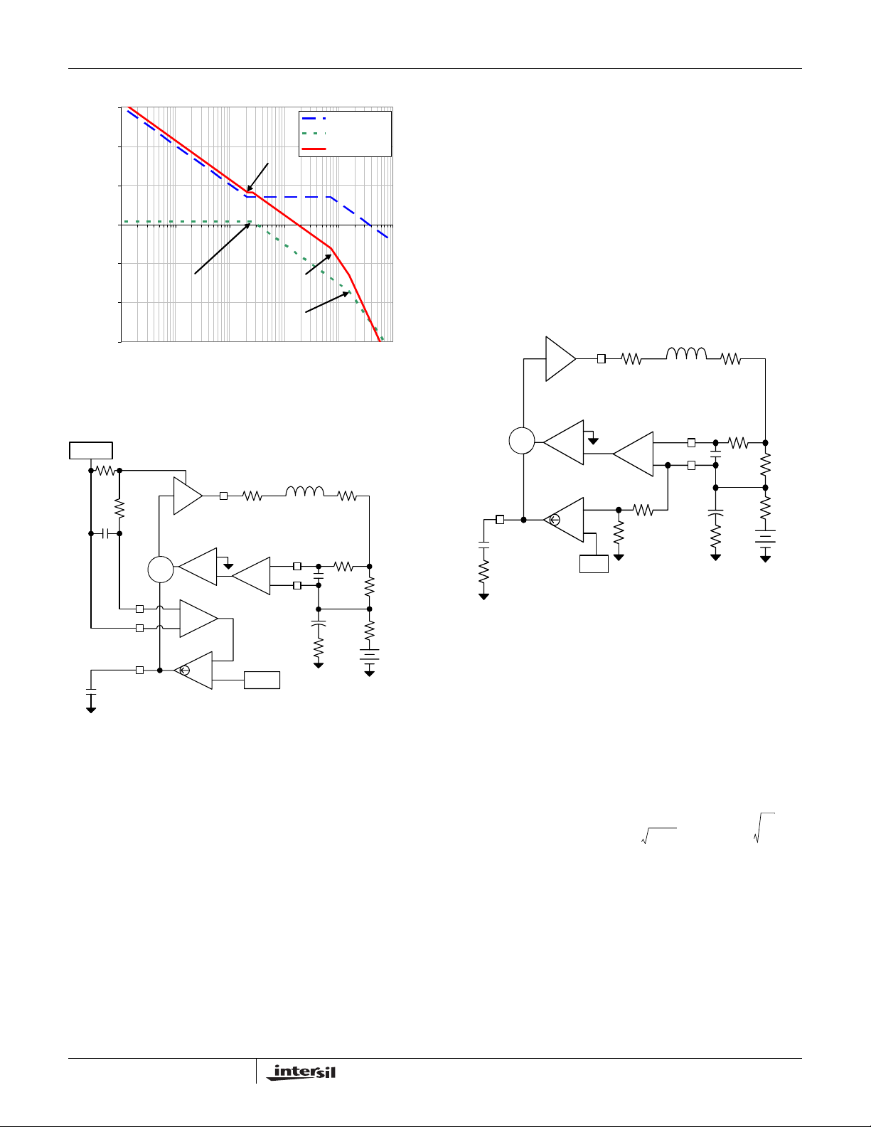
The Bode plot of the loop gain, the compensator gain and
the power stage gain is shown in Figure 22.
Adapter Current Limit Control Loop
If the combined battery charge current and system load
F
ZERO
⋅()
2π C
ICOMP
gm2 50μAV⁄=
(EQ. 17)
4gm2⋅
---------------------------------------
=
Placing this zero at a frequency equal to the pole calculated
in Equation 16 will result in maximum gain at low frequencies
and phase margin near 90°. If the zero is at a higher
current draws current that equals the adapter current limit
set by the InputCurrent register, ISL88731A will reduce the
current to the battery and/or reduce the output voltage to
hold the adapter current at the limit. Above the adapter
current limit, the minimum current buffer equals the output of
GMS and ICOMP controls the charger output. Figure 23
shows the adapter current limit control loop.
19
FN6738.1
January 7, 2009
Page 20
ISL88731A
60
40
20
0
GAIN (dB)
-20
F
-40
-60
0.01 0.1 1 10 100 1000
POLE1
FREQUE NCY (kHz)
F
ZERO
FIGURE 22. CHARGE CURRENT LOOP BODE PLOTS
DCIN
R
S1
R
F1
C
F1
S
Σ
CSSN
CSSP
ICOMP
C
ICOMP
FIGURE 23. ADAPTER CURRENT LIMIT CONTROL LOOP
11
PHASE
R
FET_RDSON
CA2
+
0.25
-
-
20
+
CA1
-
GMS
+
+
20X
-
DACS
CSOP
CSON
The loop response equations, bode plots and the selection
of C
are the same as the charge current control loop
ICOMP
with loop gain reduced by the duty cycle and the ratio of
R
. In other words, if R
S1/RS2
= RS2 and the duty cycle
S1
D = 50%, the loop gain will be 6dB lower than the loop gain
in Figure 23. This gives lower crossover frequency and
higher phase margin in this mode. If R
S1/RS2
duty cycle is 50% then the adapter current loop gain will be
identical to the gain in Figure 23.
A filter should be added between R
and CSIP and CSIN to
S1
reduce switching noise. The filter roll off frequency should be
between the crossover frequency and the switching
frequency (~100kHz).
Voltage Control Loop
When the battery is charged to the voltage set by
F
F
FILTER
POLE2
L
Compensator
Modulator
Loop
R
L_DCR
R
F2
C
F2
C
R
ESR
R
O
R
= 2 and the
S2
BAT
ChargeVoltage register the voltage error amplifier (GMV)
takes control of the output (assuming that the adapter
current is below the limit set by ACLIM). The voltage error
amplifier (GMV) discharges the capacitor on VCOMP to limit
the output voltage. The current to the battery decreases as
the cells charge to the fixed voltage and the voltage across
the internal battery resistance decreases. As battery current
decreases the two current error amplifiers (GMI and GMS)
output their maximum current and charge the capacitor on
ICOMP to its maximum voltage (limited to 0.3V above
VCOMP). With high voltage on ICOMP , the minimum voltage
buffer output equals the voltage on VCOMP.
The voltage control loop is shown in Figure 24.
PHASE
11
R
FET_RDSON
CA2
20x
R3
R4
DACV
VCOMP
C
VCOMP
R
VCOMP
S
GMV
-
-
+
0.25
Σ
+
FIGURE 24. VOLTAGE CONTROL LOOP
L
R
L_DCR
CSOP
R
F2
+
-
CSON
C
C
R
F2
O
ESR
R
S2
R
BAT
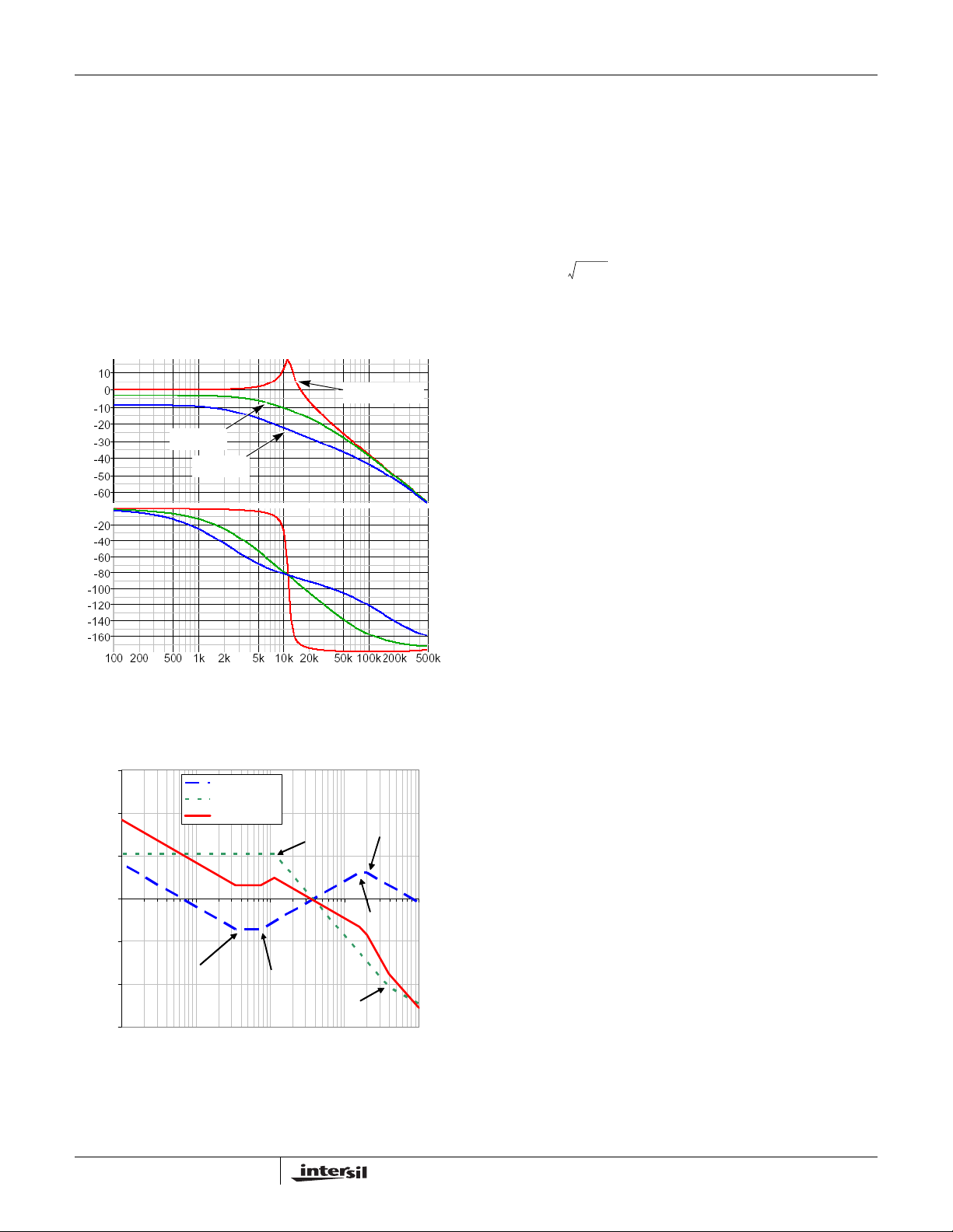
Output LC Filter Transfer Functions
The gain from the phase node to the system output and
battery depend entirely on external components. Typical
output LC filter response is shown in Figure 25. Transfer
function A
A
LC
ω
ESR
The resistance R
inductor DCR, R
battery (normally between 50mΩ and 200mΩ) The worst
case for voltage mode control is when the battery is absent.
This results in the highest Q of the LC filter and the lowest
phase margin.
The compensation network consists of the voltage error
amplifier GMV and the compensation network R
(s) is shown in Equation 22:
LC
s
⎛⎞
---------------
1
–
⎝⎠
ω
2
-------------------------
ω
LC
1
⋅()
ESRCo
SENSE
ESR
s
1++
Q⋅()
1
------------------------
ω
=
LC
is a combination of MOSFET r
O
⋅()
LC
o
and the internal resistance of the
-----------------------------------------------------------
=
⎛⎞
s
----------- -
⎜⎟
ω
⎝⎠
DP
-------------------------------- -
=
R
QR
o
DS(ON)
VCOMP
L
-------⋅=
C
o
(EQ. 22)
,
,
20
FN6738.1
January 7, 2009
Page 21
ISL88731A
C
VCOMP
frequency pole and a zero at F
which give the loop very high DC gain, a very low
. Inductor current
ZERO1
information is added to the feedback to create a second zero
F
ISL88731A add a pole at F
. The low pass filter RF2, CF2 between RS2 and
ZERO2
. R3 and R4 are internal
FILTER
divider resistors that set the DC output voltage. For a 3-cell
battery, R
= 500kΩ and R4= 100kΩ. Equations 23 through
3
30 relate the compensation network’s poles, zeros and gain
to the components in Figure 24. Figure 26 shows an
asymptotic Bode plot of the DC/DC converter’s gain vs
frequency. It is strongly recommended that F
approximately 30% of F
of F
.
LC
R
BATTERY
GAIN (dB)
PHASE (°)
FIGURE 25. FREQUENCY RESPONSE OF THE LC OUTPUT
= 200mΩ
FILTER
R
BATTERY
= 50mΩ
and F
LC
FREQUENCY
is approximately 70%
ZERO2
is
ZERO1
NO BATTERY
Compensation Break Frequency Equations
F
ZERO1
F
ZERO2
F
LC
F
FILTER
F
POLE1
F
ESR
Choose R
---------------------------------------------------------------------- -
=
⋅⋅()
2π C
⎛⎞
-----------------------------------------------
⎜⎟
2π R
⎝⎠
1
-------------------------------
=
⋅()
2π LC
-------------------------------------------
=
2π R
----------------------------------------------------
=
⋅⋅()
2π R
--------------------------------------------
=
⋅⋅()
2π C
oRESR
VCOMP
from Equation 29.
R
VCOMP
0.7 FLC⋅()2π CoR
Next choose C
calculated from Equation 30.
C
VCOMP
-------------------------------------------------------------------------- -
=
0.3 F
1
VCOMPR1COMP
R
VCOMP
⋅
SENSE
o
⋅⋅()
F2CF2
SENSECo
1
C⋅
1
1
R
⎛⎞
4
---------------------
⋅⋅=
⎜⎟
R4R3+
⎝⎠
o
gm1
⎛⎞
------------
⎝⎠
5
equal or lower than the value calculated
⎛⎞
5
⎛⎞
⋅⋅()
⋅⋅⋅=
equal or higher than the value
VCOMP
⋅()2π R
1
LC
⋅()⋅
SENSE
VCOMP
------------
⎝⎠
⎜⎟
gm1
⎝⎠
(EQ. 23)
(EQ. 24)
(EQ. 25)
(EQ. 26)
(EQ. 27)
(EQ. 28)
R
+
3R4
---------------------
R
4
(EQ. 29)
(EQ. 30)
PCB Layout Considerations
Power and Signal Layers Placement on the PCB
As a general rule, power layers should be close together,
either on the top or bottom of the board, with signal layers on
the opposite side of the board. As an example, layer
arrangement on a 4-layer board is shown below:
60
40
20
0
GAIN (dB)
-20
-40
-60
0.1 1 10 100 1000
Compensator
Modulator
Loop
F
ZERO1
FREQUE NCY (kHz)
F
ZERO2
F
F
F
FILTER
ESR
POLE1
F
LC
FIGURE 26. ASYMPTOTIC BODE PLOT OF THE VOLTAGE
CONTROL LOOP GAIN
21
1. Top La yer: signal lines, or half board for signal lines and
the other half board for power lines
2. Signal Ground
3. Power Layers: Power Ground
4. Bottom Layer: Power MOSFET, Inductors and other
Power traces
Separate the power voltage and current flowing path from
the control and logic level signal path. The controller IC will
stay on the signal layer, which is isolated by the signal
ground to the power signal traces.
Component Placement
The power MOSFET should be close to the IC so that the
gate drive signal, the LGATE, UGATE, PHASE, and BOOT,
traces can be short.
Place the components in such a way that the area under the
IC has less noise traces with high dv/dt and di/dt, such as
gate signals and phase node signals.
FN6738.1
January 7, 2009
Page 22
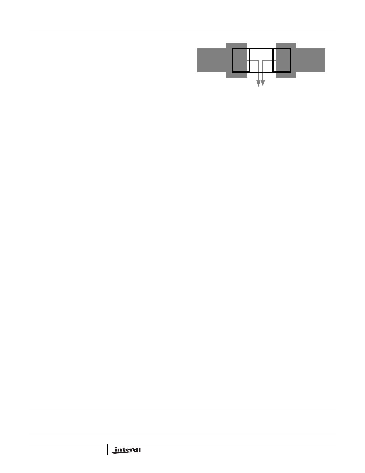
ISL88731A
Signal Ground and Power Ground Connection
At minimum, a reasonably large area of copper, which will
shield other noise couplings through the IC, should be used
as signal ground beneath the IC. The best tie-point between
the signal ground and the power ground is at the negative
side of the output capacitor on each side, where there is little
noise; a noisy trace beneath the IC is not recommended.
GND and VCC Pin
At least one high quality ceramic decoupling capacitor
should be used to cross these two pins. The decoupling
capacitor can be put close to the IC.
LGATE Pin
This is the gate drive signal for the bottom MOSFET of the
buck converter. The signal going through this trace has both
high dv/dt and high di/dt, and the peak charging and
discharging current is very high. These two traces should be
short, wide, and away from other traces. There should be no
other traces in parallel with these traces on any layer.
PGND Pin
PGND pin should be laid out to the negative side of the
relevant output capacitor with separate traces.The negative
side of the output capacitor must be close to the source node
of the bottom MOSFET. This trace is the return path of
LGATE.
PHASE Pin
This trace should be short, and positioned away from other
weak signal traces. This node has a very high dv/dt with a
voltage swing from the input voltage to ground. No trace
should be in parallel with it. This trace is also the return path
for UGATE. Connect this pin to the high-side MOSFET
source.
UGATE Pin
This pin has a square shape waveform with high dv/dt. It
provides the gate drive current to charge and discharge the
top MOSFET with high di/dt. This trace should be wide,
short, and away from other traces, similar to the LGATE.
BOOT Pin
This pin’s di/dt is as high as the UGATE; therefore, this trace
should be as short as possible.
HIGH
CURRENT
TRACE
KELVIN CONNECTION TRACES
TO THE LOW PASS FILTER AND
FIGURE 27. CURRENT SENSE RESISTOR LAYOUT
SENSE
RESISTOR
CSOP AND CSON
HIGH
CURRENT
TRACE
CSOP, CSON, CSSP and CSSN Pins
Accurate charge current and adapter current sensing is
critical for good performance. The current sense resistor
connects to the CSON and the CSOP pins through a low
pass filter with the filter capacitor very near the IC (see
Figure 2). Traces from the sense resister should start at the
pads of the sense resister and should be routed close
together, through the low pass filter and to the CSOP and
CSON pins (see Figure 27). The CSON pin is also used as
the battery voltage feedback. The traces should be routed
away from the high dv/dt and di/dt pins like PHASE, BOOT
pins. In general, the current sense resistor should be close
to the IC. These guidelines shoul d al so be fol l ow e d for th e
adapter current sense resister and CSSP and CSSN. Other
layout arrangements should be adjusted accordingly.
DCIN Pin
This pin connects to AC-adapter output voltage, and should
be less noise sensitive.
Copper Size for the Phase Node
The capacitance of PHASE should be kept very low to
minimize ringing. It would be best to limit the size of the
PHASE node copper in strict accordance with the current
and thermal management of the application.
Identify the Power and Signal Ground
The input and output capacitors of the converters, the source
terminal of the bottom switching MOSFET PGND should
connect to the power ground. The other components should
connect to signal ground. Signal and power ground are tied
together at one point.
Clamping Capacitor for Switching MOSFET
It is recommended that ceramic capacitors be used closely
connected to the drain of the high-side MOSFET, and the
All Intersil U.S. products are manufactured, assembled and tested utilizing ISO9000 quality systems.
Intersil Corporation’s quality certifications can be viewed at www.intersil.com/design/quality
Intersil products are sold by description only. Intersil Corporation reserves the right to make changes in circuit design, software and/or specifications at any time without
notice. Accordingly, the reader is cautioned to verify that data sheets are current before placing orders. Information furnished by Intersil is believed to be accurate and
reliable. However, no responsibility is assumed by Intersil or its subsidiaries for its use; nor for any infringements of patents or other rights of third parties which may result
from its use. No license is granted by implicat ion or oth erwise u nde r any p a tent or p at ent r ights of Intersil or its subsidiari es.
For information regarding Intersil Corporation and its products, see www.intersil.com
22
FN6738.1
January 7, 2009
Page 23
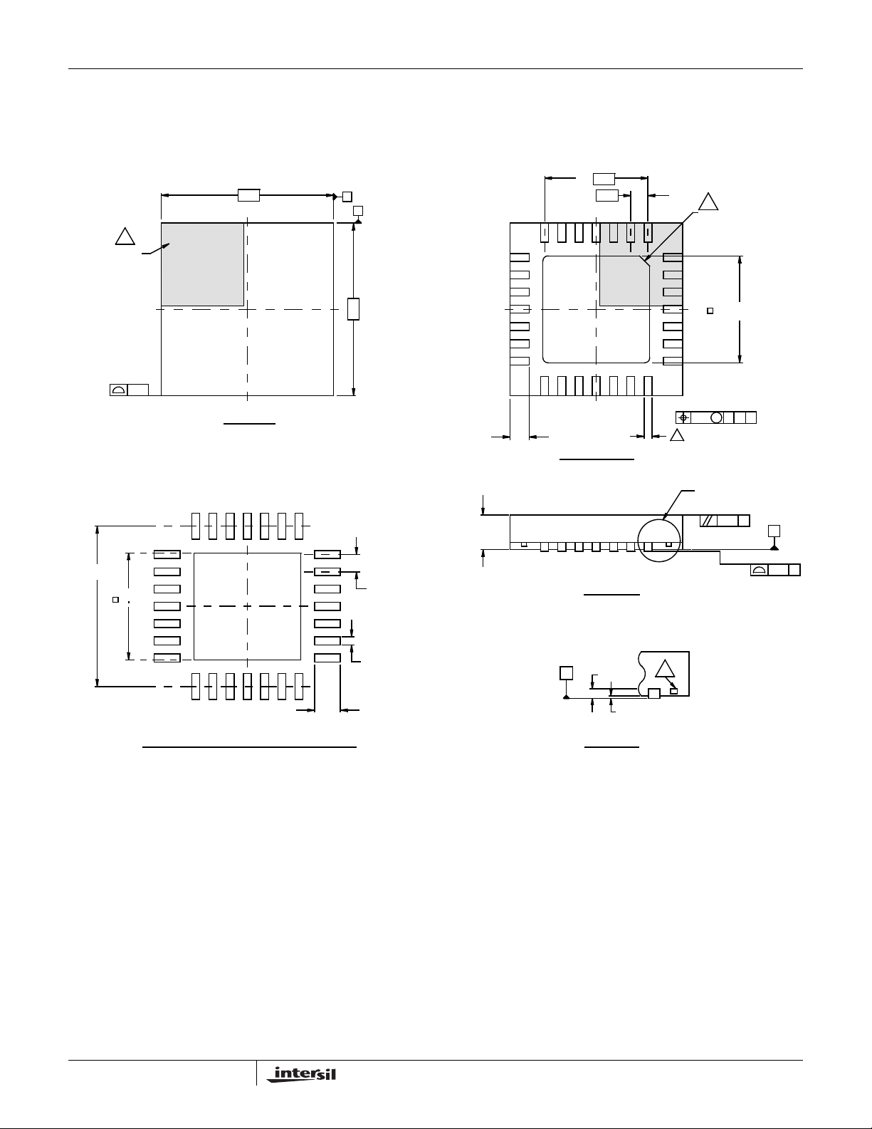
Package Outline Drawing
L28.5x5B
28 LEAD THIN QUAD FLAT NO-LEAD PLASTIC PACKAGE
Rev 1, 10/07
6
PIN 1
INDEX AREA
5.00
A
B
ISL88731A
21
22
4X
24X
3.0
0.50
28
1
6
PIN #1 INDEX AREA
(4X) 0.15
( 4. 65 TYP )
( 3. 25)
TOP VIEW
TYPICAL RECOMMENDED LAND PATTERN
5.00
( 24X 0 . 50)
(28X 0 . 25 )
( 28X 0 . 75)
0 . 75 ± 0.05
3 .25 ± 0 . 10
15
14
28X 0.55 ± 0.05 4
BOTTOM VIEW
BOTTOM VIEW
8
7
A
M0.10 C B
28X 0.25 ± 0.05
SEE DETAIL "X"
C
0.10
BASE PLANE
SEATING PLANE
C
0.08 C
SIDE VIEW
0 . 2 REF
C
0 . 00 MIN.
0 . 05 MAX.
5
DETAIL "X"
23
NOTES:
Dimensions are in millimeters.1.
Dimensions in ( ) for Reference Only.
2.
Dimensioning and tolerancing conform to AMSE Y14.5m-1994.
3.
Unless otherwise specified, tolerance : Decimal ± 0.05
4.
Dimension b applies to the metallized terminal and is measured
between 0.15mm and 0.30mm from the terminal tip.
Tiebar shown (if present) is a non-functional feature.
5.
The configuration of the pin #1 identifier is optional, but must be
6.
located within the zone indicated. The pin #1 identifier may be
either a mold or mark feature.
FN6738.1
January 7, 2009
 Loading...