

Page 1
®
www.BDTIC.com/Intersil
ISL83220E
Data Sheet April 27, 2006
±15kV ESD Protected, +3V to +5.5V,
1Microamp, 250kbps, RS-232
Transmitters/Receivers
The Intersil ISL83220E is a 3.0V to 5.5V powered RS-232
transmitter/receiver which meets ElA/TIA-232 and V.28/V.24
specifications, even at V
±15kV ESD protection (IEC61000-4-2 Air Gap and Human
Body Model) on transmitter outputs and receiver inputs
(RS-232 pins). Targeted applications are PDAs, Palmtops,
and notebook and laptop computers where the low
operational, and even lower standby, power consumption is
critical. Efficient on-chip charge pumps, coupled with a
manual powerdown function, reduce the standby supply
current to a 1μA trickle. Small footprint packaging, and the
use of small, low value capacitors ensure board space
savings as well. Data rates greater than 250kbps are
guaranteed at worst case load conditions. This family is fully
compatible with 3.3V only systems, mixed 3.3V and 5.0V
systems, and 5.0V only systems.
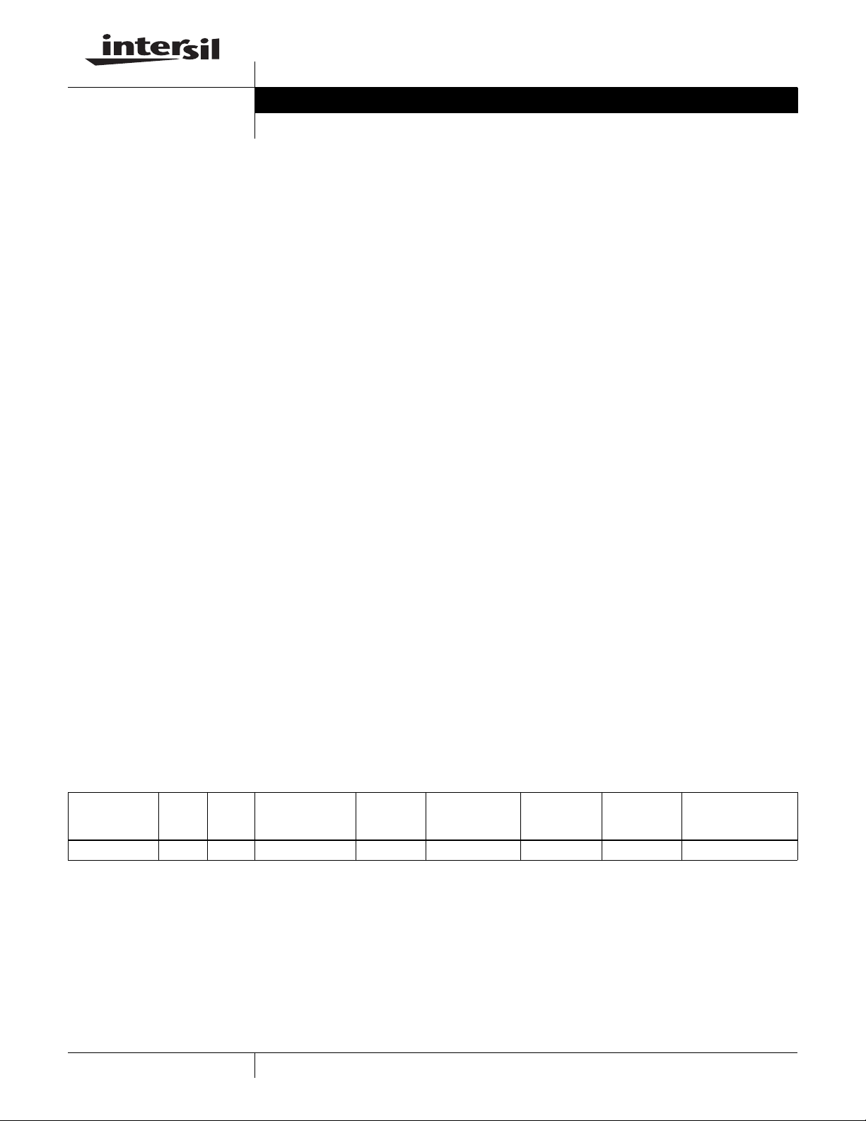
Table 1 summarizes the features of the ISL83320E, while
Application Note AN9863 summarizes the features of each
device comprising the ICL32XXE 3V family.
= 3.0V. Additionally, it provides
CC
FN6011.5
Features
• Pb-Free Plus Anneal Available (RoHS Compliant)
• ESD Protection for RS-232 I/O Pins to
• Drop in Replacement for SP3220E
• Meets EIA/TIA-232 and V.28/V.24 Specifications at 3V
• RS-232 Compatible Outputs at 2.7V
• Latch-Up Free
• On-Chip Voltage Converters Require Only Four External
0.1μF Capacitors
• Manual Powerdown Feature with Receivers Active
• Separate Receiver Enable Pin
and TX Hysteresis For Improved Noise Immunity
•R
X
• Guaranteed Minimum Data Rate . . . . . . . . . . . . . 250kbps
• Guaranteed Minimum Slew Rate . . . . . . . . . . . . . . . 6V/μs
• Wide Power Supply Range . . . . . . . Single +3V to +5.5V
• Low Supply Current in Powerdown State. . . . . . . . . . .1μA
±15kV (IEC61000)
Applications
• Any System Requiring RS-232 Communication Ports
- Battery Powered, Hand-Held, and Portable Equipment
- Laptop Computers, Notebooks, Palmtops
- Modems, Printers and other Peripherals
- Digital Cameras
- Cellular/Mobile Phones
Related Literature
• Technical Brief TB363 “Guidelines for Handling and
Processing Moisture Sensitive Surface Mount Devices
(SMDs)”
TABLE 1. SUMMARY OF FEATURES
NO. OF
PART NUMBER
NO. OF
ISL83220E 1 1 0 250 Yes No Yes No
Tx.
NO. OF
Rx.
MONITOR Rx.
(R
)
OUTB
DATA
RATE
(kbps)
Rx. ENABLE
FUNCTION?
READY
OUTPUT?
MANUAL
POWER-
DOWN?
AUTOMATIC
POWERDOWN
FUNCTION?
1
CAUTION: These devices are sensitive to electrostatic discharge; follow proper IC Handling Procedures.
1-888-INTERSIL or 1-888-468-3774
| Intersil (and design) is a registered trademark of Intersil Americas Inc.
All other trademarks mentioned are the property of their respective owners.
Copyright © Intersil Americas Inc. 2004, 2006. All Rights Reserved
Page 2
ISL83220E
www.BDTIC.com/Intersil
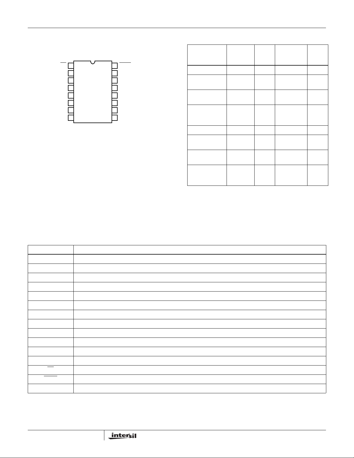
Pinout
C1+
C2+
R1
ISL83220E (TSSOP)
EN
1
2
3
V+
4
C1-
5
C2-
6
V-
7
8
IN
TOP VIEW
Ordering Information
TEMP.
PART
16
V
15
CC
GND
14
T1
13
OUT
N.C.
12
T1
11
IN
N.C.
10
R1
9
OUT
ISL83220ECV 83220ECV 0 to 70 16 Ld TSSOP M16.173
ISL83220ECV-T 83220ECV 0 to 70 16 Ld TSSOP
ISL83220ECVZ
(See Note)
ISL83220ECVZ-T
(See Note)
SHDN
PART NUMBER
MARKING
83220ECVZ 0 to 70 16 Ld TSSOP
83220ECVZ 0 to 70 16 Ld TSSOP
ISL83220EIV 83220EIV -40 to 85 16 Ld TSSOP M16.173
ISL83220EIV-T 83220EIV -40 to 85 16 Ld TSSOP
ISL83220EIVZ
83220EIVZ -40 to 85 16 Ld TSSOP
(See Note)
ISL83220EIVZ-T
83220EIVZ -40 to 85 16 Ld TSSOP
(See Note)
NOTE: Intersil Pb-free plus anneal products employ special Pb-free
material sets; molding compounds/die attach materials and 100%
matte tin plate termination finish, which are RoHS compliant and
compatible with both SnPb and Pb-free soldering operations. Intersil
Pb-free products are MSL classified at Pb-free peak reflow
temperatures that meet or exceed the Pb-free requirements of
IPC/JEDEC J STD-020.
RANGE
(°C) PACKAGE
Tape and Reel
(Pb-Free)
(Pb-Free)
Tape and Reel
Tape and Reel
(Pb-Free)
(Pb-Free)
Tape and Reel
PKG.
DWG. #
M16.173
M16.173
M16.173
M16.173
M16.173
M16.173
Pin Descriptions
PIN FUNCTION
V
CC
V+ Internally generated positive transmitter supply (+5.5V).
V- Internally generated negative transmitter supply (-5.5V).
GND Ground connection.
C1+ External capacitor (voltage doubler) is connected to this lead.
C1- External capacitor (voltage doubler) is connected to this lead.
C2+ External capacitor (voltage inverter) is connected to this lead.
C2- External capacitor (voltage inverter) is connected to this lead.
T
IN
T
OUT
R
IN
R
OUT
EN
SHDN
N.C. No internal connection.
System power supply input (3.0V to 5.5V).
TTL/CMOS compatible transmitter Inputs.
±15kV ESD Protected, RS-232 level (nominally ±5.5V) transmitter outputs.
±15kV ESD Protected, RS-232 compatible receiver inputs.
TTL/CMOS level receiver outputs.
Active low receiver enable control; doesn’t disable R
Active low input shuts down transmitters and on-board power supply, to place device in low power mode.
OUTB
outputs.
2
Page 3
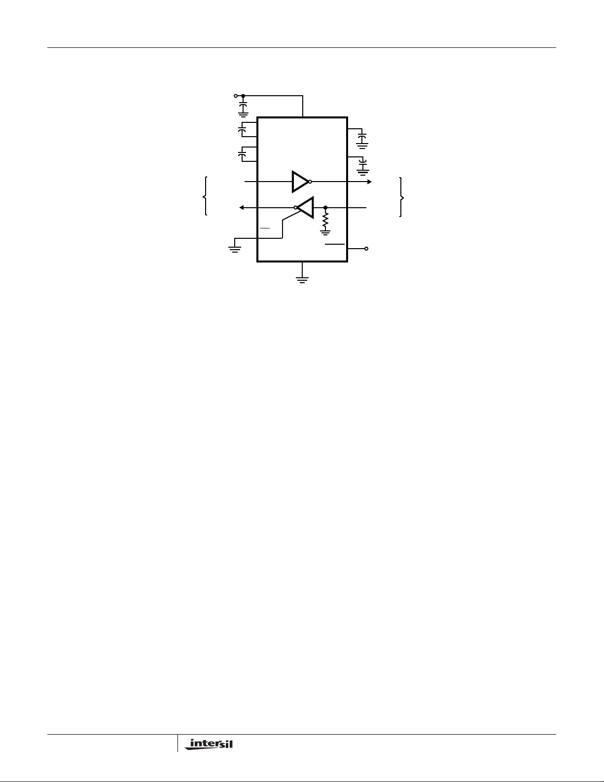
Typical Operating Circuit
www.BDTIC.com/Intersil
ISL83220E
ISL83220E
TTL/CMOS
LOGIC LEVELS
+3.3V
0.1μF
0.1μF
R1
C
C
OUT
+
0.1μF
2
C1+
1
+
4
C1-
5
2
C2+
+
6
C2-
11
IN
1
EN
V
CC
R
GND
15
3
C
3
+
V+
V-
T
1
5kΩ
1
SHDN
14
0.1μF
7
C
4
0.1μF
+
13
T1
OUTT1
89
R1
16
V
CC
RS-232
LEVELS
IN
3
Page 4
ISL83220E
www.BDTIC.com/Intersil
Absolute Maximum Ratings Thermal Information
VCC to Ground. . . . . . . . . . . . . . . . . . . . . . . . . . . . . . . . -0.3V to 6V
V+ to Ground . . . . . . . . . . . . . . . . . . . . . . . . . . . . . . . . . -0.3V to 7V
V- to Ground. . . . . . . . . . . . . . . . . . . . . . . . . . . . . . . . . +0.3V to -7V
V+ to V- . . . . . . . . . . . . . . . . . . . . . . . . . . . . . . . . . . . . . . . . . . . 14V
Input Voltages
, EN, SHDN. . . . . . . . . . . . . . . . . . . . . . . . . . . . . . -0.3V to 6V
T
IN
. . . . . . . . . . . . . . . . . . . . . . . . . . . . . . . . . . . . . . . . . . . . ±25V
R
IN
Output Voltages
. . . . . . . . . . . . . . . . . . . . . . . . . . . . . . . . . . . . . . . . . ±13.2V
T
OUT
. . . . . . . . . . . . . . . . . . . . . . . . . . . . . . . -0.3V to VCC +0.3V
R
OUT
Short Circuit Duration
. . . . . . . . . . . . . . . . . . . . . . . . . . . . . . . . . . . . . Continuous
T
OUT
ESD Rating . . . . . . . . . . . . . . . . . . . . . . . . . See Specification Table
CAUTION: Stresses above those listed in “Absolute Maximum Ratings” may cause permanent damage to the device. This is a stress only rating and operation of the
device at these or any other conditions above those indicated in the operational sections of this specification is not implied.
NOTE:
is measured with the component mounted on a low effective thermal conductivity test board in free air. See Tech Brief TB379 for details.
1. θ
JA
Thermal Resistance (Typical, Note 1)
16 Ld TSSOP Package . . . . . . . . . . . . . . . . . . . . . . 145
Maximum Junction Temperature (Plastic Package) . . . . . . . 150°C
Maximum Storage Temperature Range. . . . . . . . . . .-65°C to 150°C
Maximum Lead Temperature (Soldering 10s) . . . . . . . . . . . . 300°C
(Lead Tips Only)
θ
JA
(°C/W)
Operating Conditions
Temperature Range
ISL83220ECV . . . . . . . . . . . . . . . . . . . . . . . . . . . . . . 0°C to 70°C
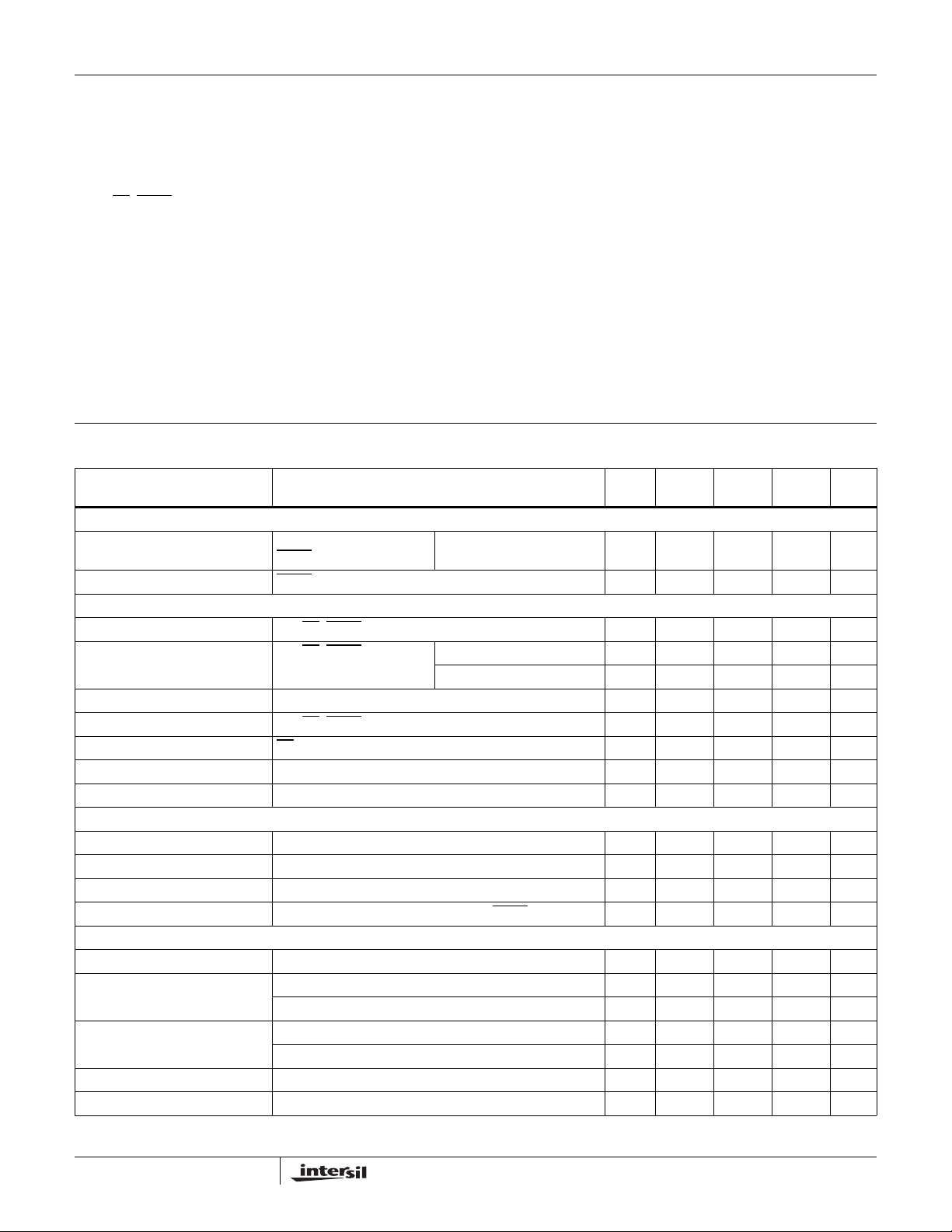
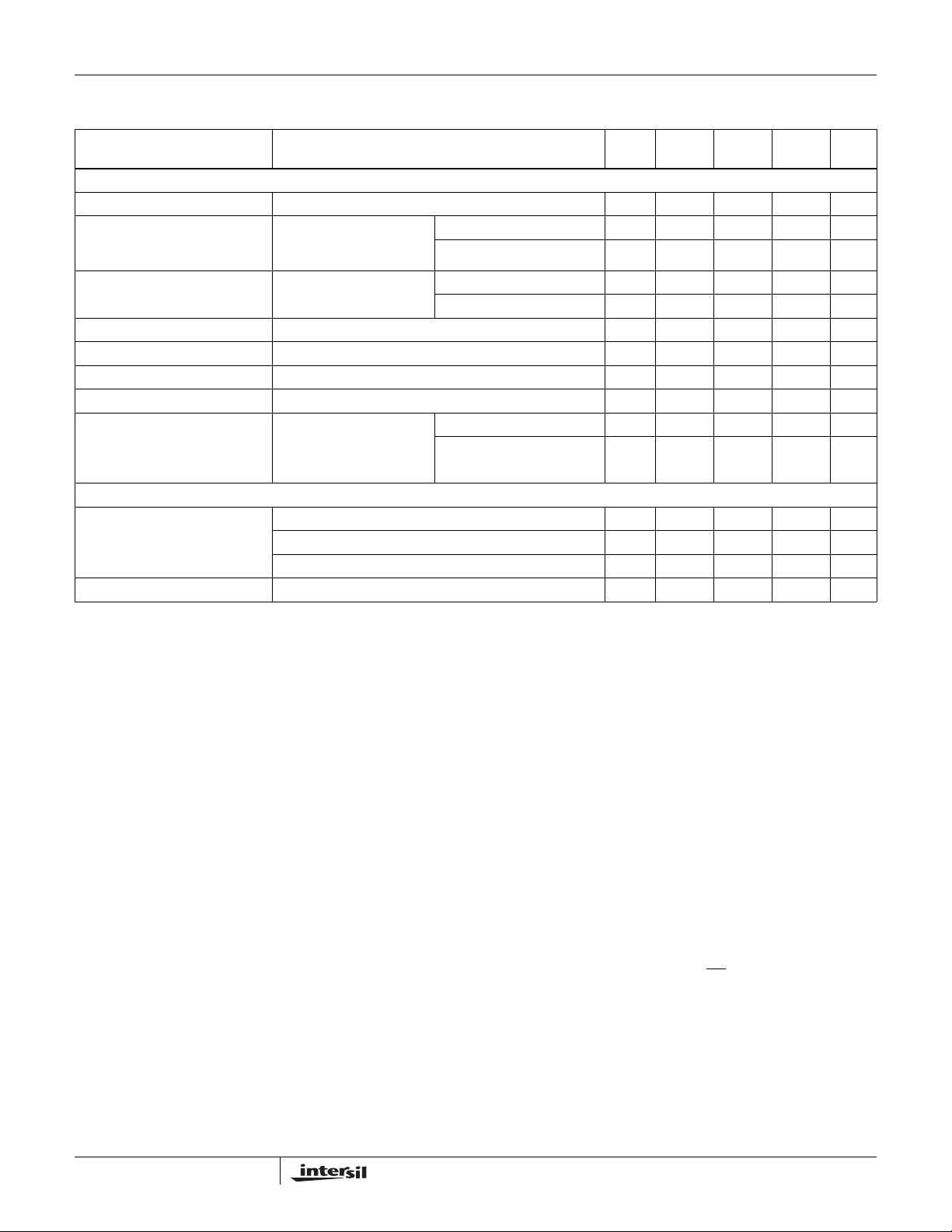
Electrical Specifications Test Conditions: V
Typicals are at T
PARAMETER TEST CONDITIONS
DC CHARACTERISTICS
Supply Current All Outputs Unloaded,
Supply Current, Powerdown SHDN
LOGIC AND TRANSMITTER INPUTS AND RECEIVER OUTPUTS
Input Logic Threshold Low T
Input Logic Threshold High T
Transmitter Input Hysteresis 25 - 0.3 V
Input Leakage Current T
Output Leakage Current EN
Output Voltage Low I
Output Voltage High I
TRANSMITTER OUTPUTS
Output Voltage Swing All Transmitter Outputs Loaded with 3kΩ to Ground Full ±5.0 ±5.4 - V
Output Resistance V
Output Short-Circuit Current V
Output Leakage Current V
RECEIVER INPUTS
Input Voltage Range Full -25 - 25 V
Input Threshold Low V
Input Threshold High V
Input Hysteresis 25 - 0.3 - V
Input Resistance Full 3 5 7 kΩ
SHDN
= V
CC
= GND 25 - 1.0 10 μA
, EN, SHDN Full - - 0.8 V
IN
, EN, SHDN VCC = 3.3V Full 2.0 - - V
IN
, EN, SHDN Full - ±0.01 ±1.0 μA
IN
= V
CC
= 1.6mA Full - - 0.4 V
OUT
= -1.0mA Full V
OUT
= V+ = V- = 0V, Transmitter Output = ±2V Full 300 10M - Ω
CC
= 0V Full - ±35 ±60 mA
OUT
= ±12V, VCC = 0V or 3V to 5.5V, SHDN = GND Full - - ±25 μA
OUT
= 3.3V Full 0.6 1.2 - V
CC
= 5.0V Full 0.8 1.5 - V
V
CC
= 3.3V Full - 1.5 2.4 V
CC
= 5.0V Full - 1.8 2.4 V
V
CC
= 3V to 5.5V, C1 - C4 = 0.1μF; Unless Otherwise Specified.
CC
= 25°C
A
TEMP
(°C) MIN TYP MAX UNITS
VCC = 3.15V 25 - 0.3 1.0 mA
= 5.0V Full 2.4 - - V
V
CC
Full - ±0.05 ±10 μA
CC
-0.6 V
-0.1 - V
CC
4
Page 5
ISL83220E
www.BDTIC.com/Intersil
Electrical Specifications Test Conditions: V
Typicals are at T
PARAMETER TEST CONDITIONS
TIMING CHARACTERISTICS
Maximum Data Rate R
Transmitter Propagation Delay Transmitter Input to
Receiver Propagation Delay Receiver Input to Receiver
Receiver Output Enable Time Normal Operation 25 - 200 - ns
Receiver Output Disable Time Normal Operation 25 - 200 - ns
Transmitter Skew t
Receiver Skew t
Transition Region Slew Rate V
ESD PERFORMANCE
RS-232 Pins (T
All Other Pins Human Body Model 25 - ±3-kV
NOTE:
2. Transmitter skew is measured at the transmitter zero crossing points.
, RIN) Human Body Model 25 - ±15 - kV
OUT
= 3kΩ, CL = 1000pF, One Transmitter Switching Full 250 500 - kbps
L
Transmitter Output,
= 3kΩ, CL = 1000pF
R
L
Output, C
PHL
PHL
CC
= 3kΩ to 7kΩ,
R
L
Measured From 3V to -3V or
-3V to 3V
IEC61000-4-2 Contact Discharge 25 - ±8-kV
IEC61000-4-2 Air Gap Discharge 25 - ±15 - kV
= 150pF
L
- t
(Note 2) 25 - 100 500 ns
PLH
- t
PLH
= 3.3V,
= 3V to 5.5V, C1 - C4 = 0.1μF; Unless Otherwise Specified.
CC
= 25°C (Continued)
A
TEMP
(°C) MIN TYP MAX UNITS
t
PHL
t
PLH
t
PHL
t
PLH
= 150pF to 2500pF 25 4 - 30 V/μs
C
L
= 150pF to 1000pF 25 6 - 30 V/μs
C
L
25 - 1.0 - μs
25 - 1.0 - μs
25 - 0.20 - μs
25 - 0.30 - μs
Full - 100 1000 ns
Detailed Description
The ISL83220E operates from a single +3V to +5.5V supply,
guarantees a 250kbps minimum data rate, requires only four
small external 0.1μF capacitors, features low power
consumption, and meets all ElA RS-232C and V.28
specifications. The circuit is divided into three sections: The
charge pump, the transmitter, and the receiver.
Charge-Pump
Intersil’s new 3.3V family utilizes regulated on-chip dual
charge pumps as voltage doublers, and voltage inverters to
generate ±5.5V transmitter supplies from a V
low as 3.0V . This allows these device s to maint ai n RS-232
compliant output levels over the ±10% tolerance range of
3.3V powered systems. The efficient on-chip power supplies
require only four small, external 0.1μF capacitors for the
voltage doubler and inverter functions, even at V
The charg e pump s operate discontinuously (i.e., they turn off
as soon as the V+ and V- supplies are pumped up to the
nominal values), resulting in significant power savings.
Transmitters
The transmitters are proprietary, low dropout, inverting
drivers that translate TTL/CMOS inputs to EIA/TIA-232
output levels. Coupled with the on-chip ±5.5V supplies,
supply as
CC
CC
= 3.3V.
these transmitters deliver true RS-232 levels over a wide
range of single supply system voltages.
The transmitter output disables and assumes a high
impedance state when the device enters the powerdown
mode (see T able 2). This output may be driven to ±12V when
disabled.
All devices guarantee a 250kbps data rate for full load
conditions (3kΩ and 1000pF), V
typical conditions of V
≥ 3.3V, RL = 3kΩ, and CL = 250pF,
CC
≥ 3.0V. Under more
CC
the ISL83220E easily operates at 900kbps.
Transmitter inputs float if left unconnected, and may cause
I
increases.
CC
Receivers
The ISL83220E device contains a standard inverting
receiver that three-states via the EN
convert RS-232 signals to CMOS output levels and accept
inputs up to ±25V while presenting the required 3kΩ to 7kΩ
input impedance (see Figure 1) even if the power is off
(V
= 0V). The receiver’s Schmitt trigger input stage uses
CC
hysteresis to increase noise immunity and decrease errors
due to slow input signal transitions.
control line. Receivers
5
Page 6
ISL83220E
www.BDTIC.com/Intersil
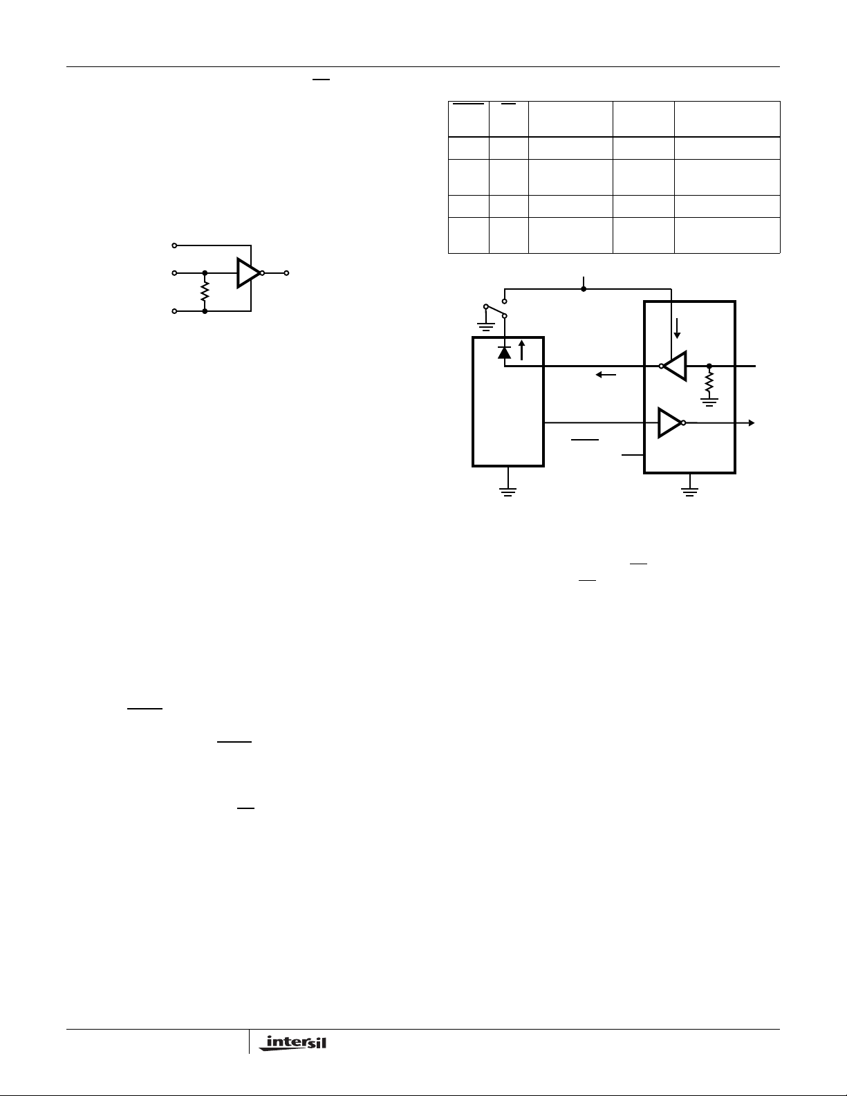
The ISL83220E receiver disables only when EN is driven
high. (see Table 2). This allows the receiver to monitor
external devices, like a modem, even when the ISL83220E
is in its 1
μA powerdown state.
Standard receivers driving powered down peripherals must
be disabled to prevent current flow through the peripheral’s
protection diodes (see Figure 2). This renders them useless
for wake up functions.
V
CC
R
1IN
-25V ≤ V
FIGURE 1. INVERTING RECEIVER CONNECTIONS
RIN
≤ +25V
GND
5kΩ
R
GND ≤ V
1OUT
ROUT
≤ V
CC
Operation Down to 2.7V
ISL83220E transmitter outputs meet RS-562 levels (±3.7V),
at the full data rate, with V
as low as 2.7V. RS-562 levels
CC
typically ensure interoperability with RS-232 devices.
Powerdown Functionality
This 3V family of RS-232 interface devices requires a
nominal supply current of 0.3mA during normal operation
(not in powerdown mode), which is considerably less than
the 5mA to 11mA current required of 5V RS-232 devices.
The already low current requirement drops significantly
when the device enters powerdown mode. In powerdown,
supply current drops to 1μA, because the on-chip charge
pump turns off (V+ collapses to V
and the transmitter outputs three-state. This micro-power
mode makes these devices ideal for battery powered and
portable applications.
Software Controlled (Manual) Powerdown
On the ISL83220E, the powerdown control is via a simple
shutdown (SHDN
operation, while driving it low forces the IC into it’s
powerdown state. Connect SHDN
function isn’t needed. Note that the receiver output remains
enabled during shutdown (see Table 2). For the lowest
power consumption during powerdown, the receiver should
also be disabled by driving the EN
section). The time to recover from manual powerdown mode
is typically 100μs.
) pin. Driving this pin high enables normal
, V- collapses to GND),
CC
to VCC if the powerdown
input high (see next
TABLE 2. POWERDOWN AND ENABLE LOGIC TRUTH TABLE
EN
INPUT
V
CC
DOWN
UART
GND
PERIPHERAL
TRANSMITTER
OUTPUT
V
CC
Rx
Tx
SHDN
SHDN
INPUT
L L High-Z Active Manual Powerdown
L H High-Z High-Z Manual Powerdown
H L Active Active Normal Operation
H H Active High-Z Normal Operation
POWERED
FIGURE 2. POWER DRAIN THROUGH POWERED DOWN
V
OUT = VCC
= GND
RECEIVER
OUTPUT
RS-232 CHIP
MODE OF
OPERATION
w/Rcvr. Disabled
w/Rcvr. Disabled
V
CC
CURRENT
FLOW
OLD
Receiver ENABLE Control
The ISL83220E also features an EN input to control the
receiver output. Driving EN
high disables the receiver output
placing it in a high impedance state. This is useful to
eliminate supply current, due to a receiver output forward
biasing the protection diode, when driving the input of a
powered down (V
= GND) peripheral (see Figure 2).
CC
Capacitor Selection
The charge pumps require 0.1μF capacitors for 3.3V
operation. Do not use values smaller than 0.1
the capacitor values (by a factor of 2) reduces ripple on the
transmitter outputs and slightly reduces power consumption.
When using minimum required capacitor values, make sure
that capacitor values do not degrade excessively with
temperature. If in doubt, use capacitors with a larger nominal
value. The capacitor’s equivalent series resistance (ESR)
usually rises at low temperatures and it influences the
amount of ripple on V+ and V
-.
μF. Increasing
Power Supply Decoupling
In most circumstances a 0.1μF bypass capacitor is
adequate. In applications that are particularly sensitive to
power supply noise, decouple V
capacitor of the same value as the charge-pump cap acitor C
Connect the bypass capacitor as close as possible to the IC.
6
to ground with a
CC
.
1
Page 7
ISL83220E
www.BDTIC.com/Intersil
Transmitter Output when Exiting
Powerdown
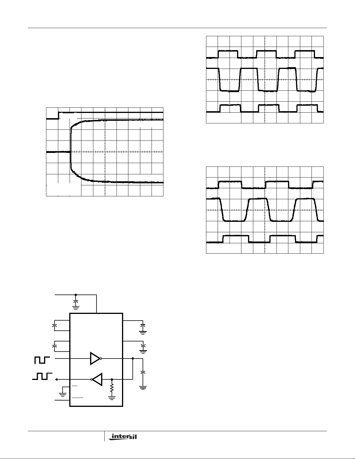
Figure 3 shows the response of the transmitter output when
exiting powerdown mode. As it activates, the transmitter
output properly goes to RS-232 levels, with no glitching,
ringing, nor undesirable transients. The transmitter is loaded
with 3kΩ in parallel with 2500pF. Note that the transmitter
enables only when the magnitude of the supplies exceed
approximately 3V.
5V/DIV
2V/DIV
FIGURE 3. TRANSMITTER OUTPUT WHEN EXITING
SHDN
TIN = LOW
TIN = HIGH
VCC = +3.3V
C1 - C4 = 0.1µF
TIME (20µs/DIV)
POWERDOWN
5V/DIV
T1
T1
OUT
R1
OUT
5V/DIV
T1
T1
OUT
IN
VCC = +3.3V
C1 - C4 = 0.1µF
5µs/DIV
FIGURE 5. LOOPBACK TEST AT 120kbps
IN
High Data Rates
The ISL83220E maintains the RS-232 ±5V minimum
transmitter output voltages even at high data rates. Figure 4
details a transmitter loopback test circuit, and Figure 5
illustrates the loopback test result at 120kbps. For this test,
the transmitter is driving an RS-232 load in parallel with
1000pF, at 120kbps. Figure 6 shows the loopback results for
the transmitter driving 1000pF and an RS-232 load at
250kbps.
V
CC
0.1μF
+
C
1
+
C
2
C1+
C1-
C2+
C2-
T
IN
R
EN
OUT
+
V
CC
ISL83220E
T
OUT
V+
V-
R
IN
5K
+
C
3
C
4
+
1000pF
R1
OUT
VCC = +3.3V
C1 - C4 = 0.1µF
2µs/DIV
FIGURE 6. LOOPBACK TEST AT 250kbps
Interconnection with 3V and 5V Logic
The ISL83220E directly interfaces with 5V CMOS and TTL
logic families. Nevertheless, with the device at 3.3V, and the
logic supply at 5V, AC, HC, and CD4000 outputs can drive
ISL83220E inputs, but ISL83220E outputs do not reach the
minimum V
information.
for these logic families. See Table 4 for more
IH
V
CC
SHDN
FIGURE 4. TRANSMITTER LOOPBACK TEST CIRCUIT
7
Page 8
ISL83220E
www.BDTIC.com/Intersil
TABLE 3. LOGIC FA MILY COMP ATIBILITY WITH V ARIOUS
SUPPLY VOLTAGES
SYSTEM
POWER-SUPPLY
VOLTAGE
(V)
3.3 3.3 Compatible with all CMOS
5 5 Compatible with all TTL and
5 3.3 Compatible with ACT and HCT
V
CC
SUPPLY
VOLTAGE
(V) COMPATIBILITY
families.
CMOS logic families.
CMOS, and with TTL.
ISL83220E outputs are
incompatible with AC, HC, and
CD4000 CMOS inputs.
±15kV ESD Protection
All pins on ISL8XXX devices include ESD protecti on
structures, but the ISL8XXXE family incorporates advanced
structures which allow the RS-232 pins (transmitter outputs
and receiver inputs) to survive ESD events up to ±15kV. The
RS-232 pins are particularly vulnerable to ESD damage
because they typically connect to an exposed port on the
exterior of the finished product. Simply touching the port
pins, or connecting a cable, can cause an ESD event that
might destroy unprotected ICs. These new ESD structures
protect the device whether or not it is powe re d up , protect
without allowing any latchup mechanism to activate, and
don’t interfere with RS-232 signals as large as ±25V.
Human Body Model (HBM) Testing
As the name implies, this test method emulates the ESD
event delivered to an IC during human handling. The tester
delivers the charge through a 1.5kΩ current limiting resistor,
making the test less severe than the IEC61000 test which
utilizes a 330Ω limiting resistor. The HBM method
determines an IC’s ability to withstand the ESD transients
typically present during handling and manufacturing. Due to
the random nature of these events, each pin is tested with
respect to all other pins. The RS-232 pins on “E” family
devices can withstand HBM ESD events to ±15kV.
IEC61000-4-2 Testing
The IEC61000 test method applies to finished equipment,
rather than to an individual IC. Therefore, the pins most likely
to suffer an ESD event are those that are exposed to the
outside world (the RS-232 pins in this case), and the IC is
tested in its typical application configuration (power applied)
rather than testing each pin-to-pin combination. The lower
current limiting resistor coupled with the larger charge
storage capacitor yields a test that is much more severe than
the HBM test. The extra ESD protection built into this
device’s RS-232 pins allows the design of equipment
meeting level 4 criteria without the need for additional board
level protection on the RS-232 port.
AIR-GAP DISCHARGE TEST METHOD
For this test method, a charged probe tip moves toward the
IC pin until the voltage arcs to it. The current waveform
delivered to the IC pin depends on approach speed,
humidity, temperature, etc., so it is difficult to obtain
repeatable results. The “E” device RS-232 pins withstand
±15kV air-gap discharges.
CONTACT DISCHARGE TEST METHOD
During the contact discharge test, the probe contacts the
tested pin before the probe tip is energized, thereby
eliminating the variables associated with the air-gap
discharge. The result is a more repeatable and predictable
test, but equipment limits prevent testing devices at voltages
higher than ±8kV . All “E” family devices survive ±8kV contact
discharges on the RS-232 pins.
Typical Performance Curves V
6
4
2
TRANSMITTER AT 250kbps
0
-2
-4
TRANSMITTER OUTPUT VOLTAGE (V)
-6
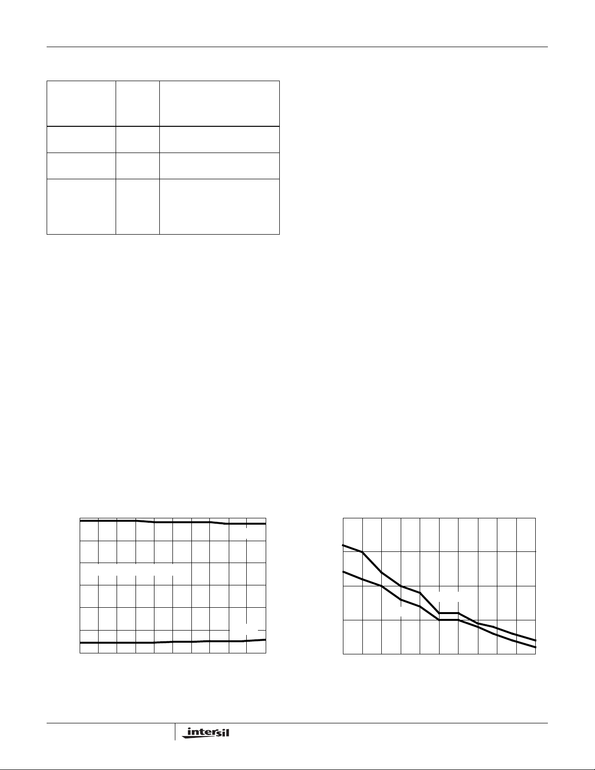
FIGURE 7. TRANSMITTER OUTPUT VOLTAGE vs LOAD
1000 2000 3000 4000 50000
LOAD CAPACITANCE (pF)
CAPACITANCE
= 3.3V, TA = 25°C
CC
V
+
OUT
V
-
OUT
25
20
15
SLEW RATE (V/µs)
10
5
0 1000 2000 3000 4000 5000
FIGURE 8. SLEW RATE vs LOAD CAPACITANCE
8
-SLEW
+SLEW
LOAD CAPACITANCE (pF)
Page 9
ISL83220E
www.BDTIC.com/Intersil
Typical Performance Curves V
45
40
35
30
25
20
15
SUPPLY CURRENT (mA)
10
5
0
0 1000 2000 3000 4000 5000
LOAD CAPACITANCE (pF)
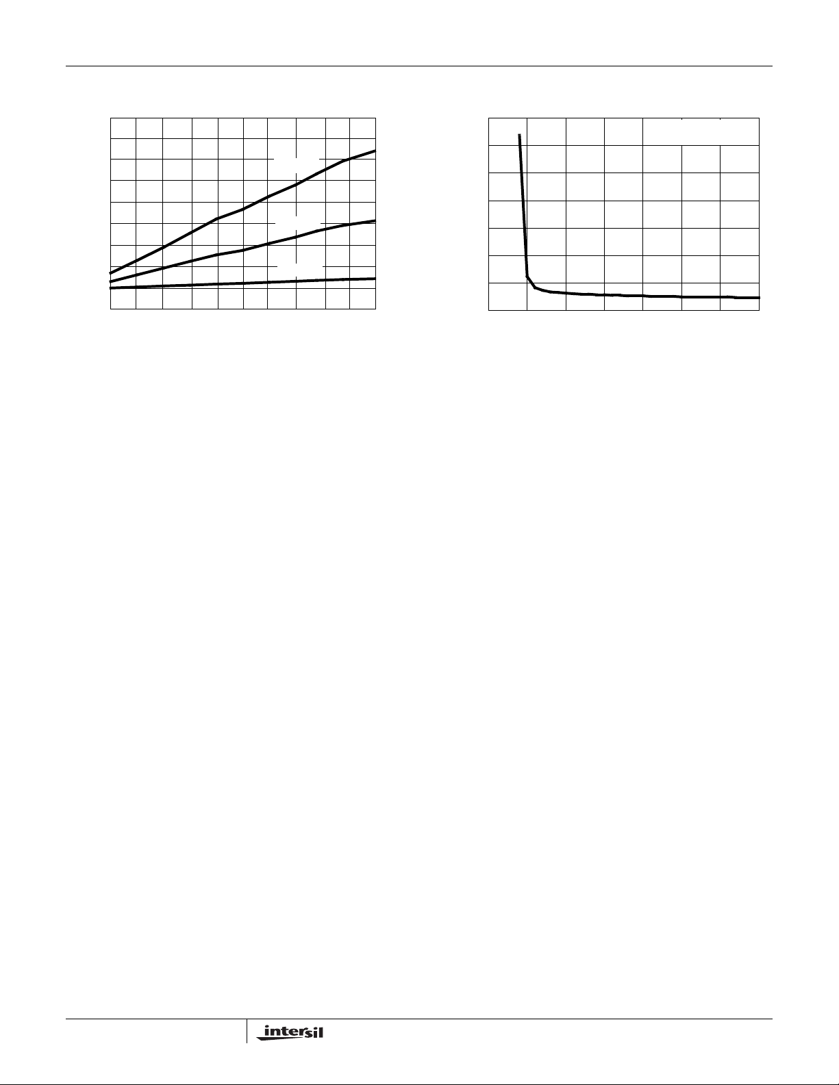
FIGURE 9. SUPPLY CURRENT vs LOAD CAP ACITANCE
WHEN TRANSMITTING DATA
= 3.3V, TA = 25°C (Continued)
CC
250kbps
120kbps
20kbps
Die Characteristics
SUBSTRATE POTENTIAL (POWERED UP):
GND
3.5
3.0
2.5
2.0
1.5
1.0
SUPPLY CURRENT (mA)
0.5
0
2.5 3.0 3.5 4.0 4.5 5.0 5.5 6.0
SUPPLY VOLTAGE (V)
FIGURE 10. SUPPLY CURRENT vs SUPPLY VOLTAGE
NO LOAD
ALL OUTPUTS STATIC
TRANSISTOR COUNT:
286
PROCESS:
Si Gate CMOS
9
Page 10
ISL83220E
www.BDTIC.com/Intersil
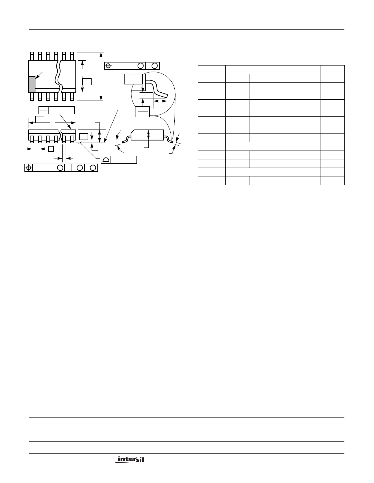
Thin Shrink Small Outline Plastic Packages (TSSOP)
N
INDEX
AREA
123
0.05(0.002)
-AD
e
b
0.10(0.004) C AM BS
NOTES:
1. These package dimensions are within allowable dimensions of
JEDEC MO-153-AB, Issue E.
2. Dimensioning and tolerancing per ANSI Y14.5M-1982.
3. Dimension “D” does not include mold flash, protrusions or gate
burrs. Mold flash, protrusion and gate burrs shall not exceed
0.15mm (0.006 inch) per side.
4. Dimension “E1” does not include interlead flash or protrusions.
Interlead flash and protrusions shall not exceed 0.15mm (0.006
inch) per side.
5. The chamfer on the body is optional. If it is not present, a visual
index feature must be located within the crosshatched area.
6. “L” is the length of terminal for soldering to a substrate.
7. “N” is the number of terminal positions.
8. Terminal numbers are shown for reference only.
9. Dimension “b” does not include dambar protrusion. Allowable
dambar protrusion shall be 0.08mm (0.003 inch) total in excess
of “b” dimension at maximum material condition. Minimum space
between protrusion and adjacent lead is 0.07mm (0.0027 inch).
10. Controlling dimension: MILLIMETER. Converted inch dimensions are not necessarily exact. (Angles in degrees)
E1
-B-
SEATING PLANE
A
-C-
M
0.25(0.010) BM M
E
α
A1
0.10(0.004)
GAUGE
PLANE
0.25
0.010
A2
M16.173
16 LEAD THIN SHRINK SMALL OUTLINE PLASTIC PACKAGE
INCHES MILLIMETERS
SYMBOL
A - 0.043 - 1.10 -
A1 0.002 0.006 0.05 0.15 -
L
c
A2 0.033 0.037 0.85 0.95 -
b 0.0075 0.012 0.19 0.30 9
c 0.0035 0.008 0.09 0.20 -
D 0.193 0.201 4.90 5.10 3
E1 0.169 0.177 4.30 4.50 4
e 0.026 BSC 0.65 BSC -
E 0.246 0.256 6.25 6.50 -
L 0.020 0.028 0.50 0.70 6
N16 167
o
α
0
o
8
o
0
o
8
NOTESMIN MAX MIN MAX
-
Rev. 1 2/02
All Intersil U.S. products are manufactured, assembled and tested utilizing ISO9000 quality systems.
Intersil Corporation’s quality certifications can be viewed at www.intersil.com/design/quality
Intersil products are sold by description only. Intersil Corporation reserves the right to make changes in circuit design, software and/or specifications at any time without
notice. Accordingly, the reader is cautioned to verify that data sheets are current before placing orders. Information furnished by Intersil is believed to be accurate and
reliable. However, no responsibility is assumed by Intersil or its subsidiaries for its use; nor for any infringements of patents or other rights of third parties which may result
from its use. No license is granted by implic atio n or other wise u nde r any p a tent or patent rights of Intersil or it s subs idi aries.
For information regarding Intersil Corporation and its products, see www.intersil.com
10
 Loading...