

®
www.BDTIC.com/Intersil
ISL83202
Data Sheet FN6382.0
55V, 1A Peak Current H-Bridge FET Driver
The ISL83202 is a medium-frequency H-Bridge FET driver
capable of 1A (typ) of peak drive current that is designed to
drive high- and low-side N-Channel MOSFETs in mediumvoltage applications. Optimized for PWM motor control and
uninterruptible power supply systems, the ISL83202 enables
simple and flexible bridge-based design. With typical inputto-output propagation delays as low as 25ns and with a userprogrammable dead-time range of 0.1µs to 4.5µs, the
ISL83202 is ideal for switching frequencies up to 200kHz.
The dead-time of the ISL83202 is programmable via a single
resistor. The ISL83202's four independent driver control
inputs (ALI, AHI, BLI, and BHI) allow driving of every
possible switch combination except those that would cause
a shoot-through condition. A global disable input, DIS,
overrides input control and causes the ISL83202 to refresh
the bootstrap capacitor when pulled low. Integrated
undervoltage protection and shoot-through protection ensure
reliable system operation.
The ISL83202 is available in compact 16 Ld SOIC and 16 Ld
PDIP packages and operates over the range of -55°C to
+125°C.
Ordering Information
PART
NUMBER
ISL83202IBZ
(Note)
ISL83202IBZT
(Note)
ISL83202IPZ
(Note)
NOTE: Intersil Pb-free plus anneal products employ special Pb-free
material sets; molding compounds/die attach materials and 100%
matte tin plate termination finish, which are RoHS compliant and
compatible with both SnPb and Pb-free soldering operations. Intersil
Pb-free products are MSL classified at Pb-free peak reflow
temperatures that meet or exceed the Pb-free requirements of IPC/
JEDEC J STD-020.
**Pb-free PDIPs can be used for through hole wave solder processing
only. They are not intended for use in Reflow solder processing
applications.
PART
MARKING
83202IBZ -55 to +125 16 Ld SOIC (N)
16 Ld SOIC (N) Tape and Reel
(Pb-free)
ISL83202IPZ -55 to +125 16 Ld PDIP**
TEMP.
RANGE (°C) PACKAGE
(Pb-free)
(Pb-free)
PKG.
DWG . #
M16.15
M16.15
E16.3
December 20, 2006
Features
• Independently Drives 4 N-Channel FETs in Half Bridge or
Full Bridge Configurations
• Bootstrap Supply Max Voltage: 70VDC
• Drives a 1000pF Load in Free Air at +50°C with Rise and
Fall Times of 15ns (typ)
• User-Programmable Dead Time from 0.1 to 4.5μs
• DIS (Disable) Overrides Input Control and Refreshes
Bootstrap Capacitor when Pulled Low
• Input Logic Thresholds Compatible with 5V to 15V Logic
Levels
• Shoot-Through Protection
• Undervoltage Protection
• Pb-Free Plus Anneal Available (RoHS Compliant)
Applications
• UPS Systems
• DC Motor Controls
• Full Bridge Power Supplies
• Switching Power Amplifiers
• Noise Cancellation Systems
• Battery Powered Vehicles
• Peripherals
• Medium/Large Voice Coil Motors
• Related Literature
- TB363, Guidelines for Handling and Processing
Moisture Sensitive Surface Mount Devices (SMDs)
Pinout
ISL83202
(PDIP, SOIC)
TOP VIEW
16
BHB
BHI
BLI
ALI
DEL
V
SS
AHI
DIS
1
2
3
4
5
6
7
8
BHO
BHS
15
14
BLO
13
ALO
V
12
DD
11
AHS
AHO
10
9
AHB
1
CAUTION: These devices are sensitive to electrostatic discharge; follow proper IC Handling Procedures.
1-888-INTERSIL or 1-888-468-3774
| Intersil (and design) is a registered trademark of Intersil Americas Inc.
All other trademarks mentioned are the property of their respective owners.
Copyright Intersil Americas Inc. 2006. All Rights Reserved
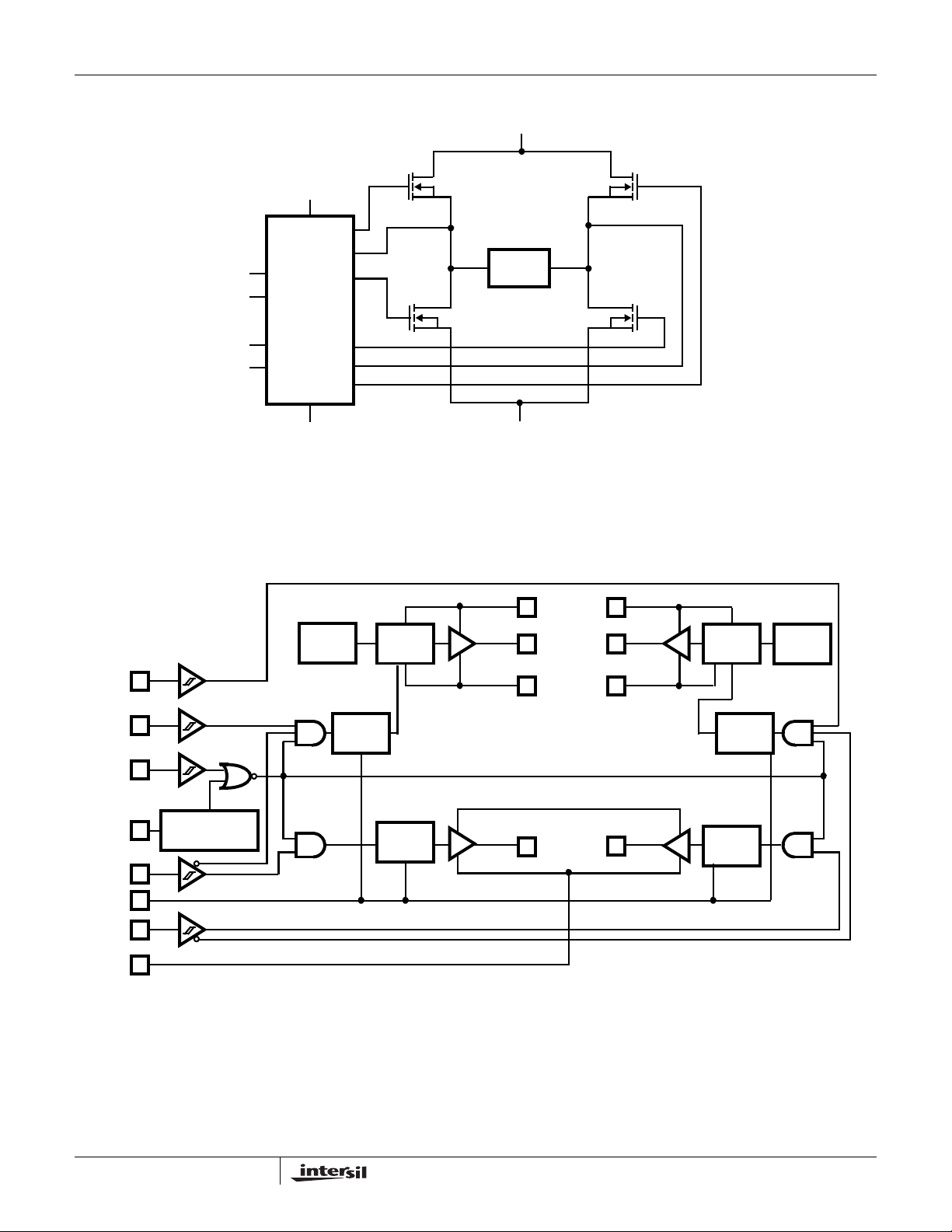
Application Block Diagram
www.BDTIC.com/Intersil
BHI
BLI
ISL83202
12V
BHO
BHS
BLO
ISL83202
55V
LOAD
ALI
AHI
Functional Block Diagram
BHI
2
AHI
7
DIS
8
12
UNDERVOLTAGE
4
5
DETECTOR
V
DD
ALI
DEL
GND
ALO
AHS
AHO
U/V
TURN-ON
DELAY
LEVEL
SHIFT
TURN-ON
DELAY
DRIVER
DRIVER
GND
10
11
13
AHB
9
AHO
AHS
ALO BLO
1
BHB
DRIVER
16
BHO
15
BHS
V
DD
DRIVER
14
LEVEL
SHIFT
TURN-ON
DELAY
TURN-ON
DELAY
U/V
BLI
3
V
6
SS
2
FN6382.0
December 20, 2006
ISL83202
www.BDTIC.com/Intersil
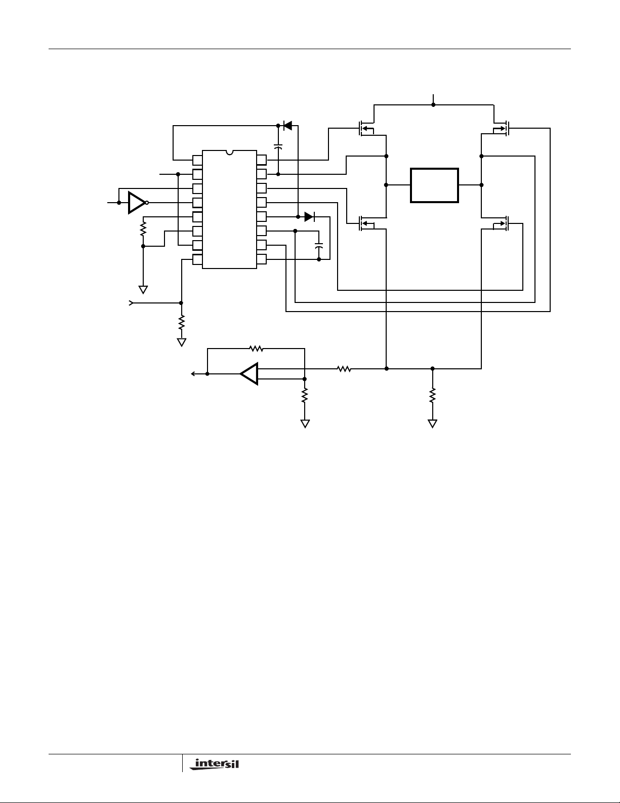
Typical Application (PWM Mode Switching)
16
BHO
BHS
15
14
BLO
13
ALO
V
AHS
SS
AHO
AHB
DD
12V
12
11
10
9
PWM
INPUT
DELAY RESISTOR
12V
DIS
1
BHB
2
BHI
3
BLI
4
ALI
5
DEL
6
V
7
AHI
8
DIS
55V
LOAD
FROM
OPTIONAL
OVERCURRENT
LATCH
TO OPTIONAL
CURRENT CONTROLLER OR
OVERCURRENT LATCH
GND
R
DIS
+
-
R
SH
GND
3
FN6382.0
December 20, 2006
ISL83202
www.BDTIC.com/Intersil
Absolute Maximum Ratings Thermal Information
Supply Voltage, VDD . . . . . . . . . . . . . . . . . . . . . . . . . . .-0.3V to 16V
Logic I/O Voltages . . . . . . . . . . . . . . . . . . . . . . . -0.3V to V
Voltage on AHS, BHS . . . . -6V (Transient) to 65V (-55°C to+150°C)
Voltage on AHB, BHB . . . . . . . . V
AHS, BHS
-0.3V to V
DD
AHS, BHS
+0.3V
+V
DD
Voltage on ALO, BLO. . . . . . . . . . . . . . . . . .VSS -0.3V to VDD +0.3V
Voltage on AHO, BHO. . . V
Current, DEL . . . . . . . . . . . . . . . . . . . . . . . . . . . . . . . . -5mA to 0mA
AHS, BHS
-0.3V to V
AHB, BHB
+0.3V Input
Phase Slew Rate . . . . . . . . . . . . . . . . . . . . . . . . . . . . . . . . . . 20V/ns
NOTE: All voltages are relative V
unless otherwise specified.
SS
Operating Conditions
Supply Voltage, VDD . . . . . . . . . . . . . . . . . . . . . . . . . +8.5V to +15V
Voltage on V
Voltage on AHB, BHB . . . . . . . . . . . . . . . . . . . . . . . . . . -1V to +55V
Voltage on AHB, BHB . . . . . . . .V
Input Current, DEL . . . . . . . . . . . . . . . . . . . . . . . . . -4mA to -100μA
CAUTION: Stresses above those listed in “Absolute Maximum Ratings” may cause permanent damage to the device. This is a stress only rating and operation of the
device at these or any other conditions above those indicated in the operational sections of this specification is not implied.
+150°C max junction temperature is intended for short periods of time to pr event sho rte ning the lif etime. Opera tio n close to +150° C ju nction ma y t rigger the shu t down of
the device even before +150°C, since this number is specified as typical.
. . . . . . . . . . . . . . . . . . . . . . . . . . . . . . -1.0V to +1.0V
SS
+7.5V to V
AHS, BHS
AHS, BHS +VDD
Thermal Resistance θ
JA
(°C/W)
SOIC Package . . . . . . . . . . . . . . . . . . . . . . . . . . . . . 115
PDIP Package* . . . . . . . . . . . . . . . . . . . . . . . . . . . . 90
Maximum Power Dissipation. . . . . . . . . . . . . . . . . . . . . . . . See Curve
Storage Temperature Range . . . . . . . . . . . . . . . . . .-65°C to +150°C
Operating Max. Junction Temperature. . . . . . . . . . . . . . . . . . +150°C
Lead Temperature (Soldering 10s) . . . . . . . . . . . . . . . . . . . . +300°C
(For SOIC - Lead Tips Only))
*Pb-free PDIPs can be used for through hole wave solder
processing only. They are not intended for use in Reflow solder
processing applications.
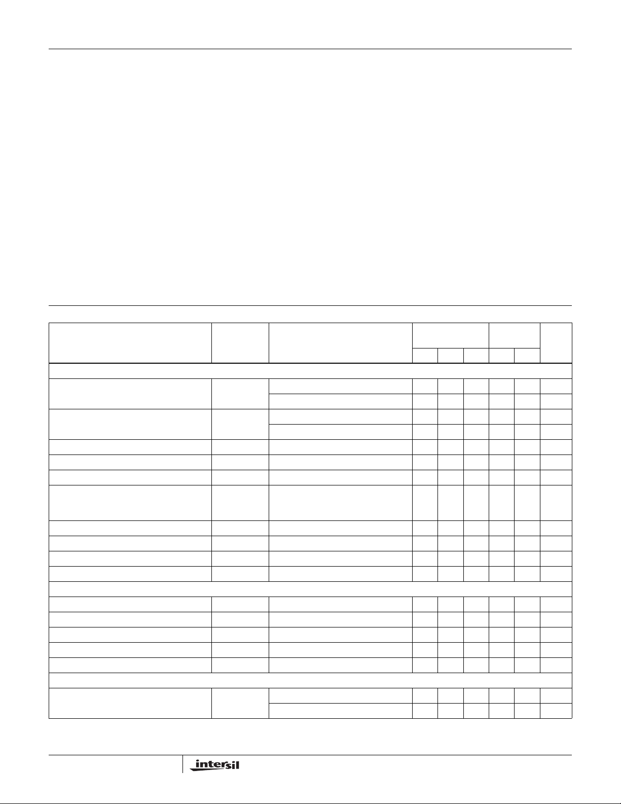
Electrical Specifications V
PARAMETER SYMBOL TEST CONDITIONS
DD
= V
AHB
= V
BHB
= 12V, VSS = V
AHS
= V
BHS
= 0V, R
DEL
= 100k
T
= +25°C
J
T
= -55°C
J
TO +150°C
UNITSMIN TYP MAX MIN MAX
SUPPLY CURRENTS AND UNDER VOLTAGE PROTECTION
Quiescent Current I
V
DD
Operating Current I
V
DD
AHB, BHB Off Quiescent Current I
AHB, BHB On Quiescent Current I
AHB, BHB Operating Current I
AHBL
AHBH
AHBO
AHS, BHS Leakage Current I
V
Rising Undervoltage Threshold V
DD
Falling Undervoltage Threshold V
V
DD
DD
DDO
, I
, I
, I
HLK
DDUV+
DDUV-
All inputs = 0V, R
All inputs = 0V, R
= 100k 1.2 2.3 3.5 0.85 4 mA
DEL
= 10k 2.2 4.0 5.5 1.9 6.0 mA
DEL
f = 50kHz, no load 1.5 2.6 4.0 1.1 4.2 mA
50kHz, no load, R
AHI = BHI = 0V 0.5 1.0 1.5 0.4 1.6 mA
BHBL
AHI = BHI = V
BHBH
f = 50kHz, CL = 1000pF .65 1.1 1.8 .45 2.0 mA
BHBO
V
= V
= V
BHS
BHB
= 55V
= 70V
AHS
V
AHB
= Not Connected
V
DD
= 10kΩ 2.5 4.0 6.4 2.1 6.6 mA
DEL
DD
65 145 240 40 250 μA
--1.0--μA
6.8 7.6 8.25 6.5 8.5 V
6.5 7.1 7.8 6.25 8.1 V
Undervoltage Hysteresis UVHYS 0.17 0.4 0.75 0.15 0.90 V
AHB, BHB Undervoltage Threshold VHBUV Referenced to AHS and BHS 5 6.0 7 4.5 7.5 V
INPUT PINS: ALI, BLI, AHI, BHI, and DIS
Low Level Input Voltage V
High Level Input Voltage V
IL
IH
Full Operating Conditions - - 1.0 - 0.8 V
Full Operating Conditions 2.5 - - 2.7 V
Input Voltage Hysteresis -35- - - mV
Low Level Input Current I
High Level Input Current I
IL
IH
VIN = 0V, Full Operating Conditions -145 -100 -60 -150 -50 μA
VIN = 5V, Full Operating Conditions -1 - +1 -10 +10 μA
TURN-ON DELAY PIN DEL
R
Dead Time T
DEAD
= 100k 2.5 4.5 8.0 2.0 8.5 μs
DEL
= 10k 0.27 0.5 0.75 0.2 0.85 μs
R
DEL
4
FN6382.0
December 20, 2006

ISL83202
www.BDTIC.com/Intersil
Electrical Specifications V
DD
= V
AHB
= V
BHB
= 12V, VSS = V
PARAMETER SYMBOL TEST CONDITIONS
GATE DRIVER OUTPUT PINS: ALO, BLO, AHO, and BHO
Low Level Output Voltage V
High Level Output Voltage V
Peak Pullup Current I
Peak Pulldown Current I
Switching Specifications V
DD
= V
AHB
OL
DD-VOHIOUT
+V
O
-V
O
= V
= 12V, VSS = V
BHB
PARAMETER SYMBOL TEST CONDITIONS
Lower Turn-off Propagation Delay
(ALI-ALO, BLI-BLO)
Upper Turn-off Propagation Delay
T
(AHI-AHO, BHI-BHO)
Lower Turn-on Propagation Delay
(ALI-ALO, BLI-BLO)
Upper Turn-on Propagation Delay
T
(AHI-AHO, BHI-BHO)
Rise Time T
Fall Time T
Minimum Input Pulse Width T
Output Pulse Response to 50ns Input Pulse
Disable Turn-off Propagation Delay
PWIN-ON/OFF
T
T
(DIS - Lower Outputs)
Disable Turn-off Propagation Delay
(DIS - Upper Outputs)
Disable Turn-on Propagation Delay
T
DISHIGH
T
(DIS - ALO and BLO)
Disable Turn-on Propagation Delay
T
(DIS- AHO and BHO)
Refresh Pulse Width (ALO and BLO) T
T
LPHL
HPHL
T
LPLH
HPLH
R
F
PWOUT
DISLOW
DLPLH
DHPLH
REF-PW
= V
BHS
= 0V, R
AHS
I
= 50mA 0.65 1.1 0.5 1.2 V
OUT
= 100k (Continued)
DEL
T
= +25°C
J
T
= -55°C
J
TO +150°C
= -50mA 0.7 1.2 0.5 1.3 V
= 0V 1.0 0.6 2.0 A
OUT
= 12V 1.0 0.6 2.0 A
OUT
= V
AHS
BHS
= 0V, R
= 100k, CL = 1000pF.
DEL
T
= +25°C
J
= -55°C TO
T
J
+150°C
- 25 50 - 70 ns
- 55 80 - 100 ns
- 40 85 - 100 ns
- 75 110 - 150 ns
-920-25ns
-920-25ns
50 - - 50 - ns
63 80 ns
- 50 80 - 90 ns
- 75 100 - 125 ns
- 40 70 - 100 ns
R
= 10k - 1.2 2 - 3 μs
DEL
375 580 900 350 950 ns
UNITSMIN TYP MAX MIN MAX
UNITSMIN TYP MAX MIN MAX
TRUTH TABLE
INPUT OUTPUT
ALI, BLI AHI, BHI VDDUV VHBUV DIS ALO, BLO AHO, BHO
XXXX1 0 0
XX1XX 0 0
0X010 0 0
1X0X0 1 0
01000 0 1
00000 0 0
NOTE: X signifies that input can be either a “1” or “0”.
5
FN6382.0
December 20, 2006

ISL83202
www.BDTIC.com/Intersil
ISL83202
Pin Descriptions
PIN
NUMBE
R SYMBOL DESCRIPTION
1 BHB B High-side Bootstrap supply. External bootstrap diode and capacitor are required. Connect cathode of bootstrap diode
and positive side of bootstrap capacitor to this pin.
2 BHI B High-side Input. Logic level input that controls BHO driver (Pin 16). BLI (Pin 3) high level input overrides BHI high level
3 BLI B Low-side Input. Logic level input that controls BLO driver (Pin 14). If BHI (Pin 2) is driven high or not connected externally
4 ALI A Low-side Input. Logic level input that controls ALO driver (Pin 13). If AHI (Pin 7) is driven high or not connected externally
5 DEL Turn-on DELay. Connect resistor from this pin to V
6V
7 AHI A High-side Input. Logic level input that controls AHO driver (Pin 10). ALI (Pin 4) high level input overrides AHI high level
8 DIS DISable input. Logic level input that when taken high sets all four outputs low. DIS high overrides all other inputs. When
9 AHB A High-side Bootstrap supply. External bootstrap diode and capacitor are required. Connect cathode of bootstrap diode
10 AHO A High-side Output. Connect to gate of A High-side power MOSFET.
11 AHS A High-side Source connection. Connect to source of A High-side power MOSFET. Connect negative side of bootstrap
12 V
13 ALO A Low-side Output. Connect to gate of A Low-side power MOSFET.
14 BLO B Low-side Output. Connect to gate of B Low-side power MOSFET.
15 BHS B High-side Source connection. Connect to source of B High-side power MOSFET. Connect negative side of bootstrap
16 BHO B High-side Output. Connect to gate of B High-side power MOSFET.
input to prevent half-bridge shoot-through, see Truth Table. DIS (Pin 8) high level input overrides BHI high level input. The
DD
DD
-2V.
DD
).
).
pin can be driven by signal levels of 0V to 15V (no greater than V
then BLI controls both BLO and BHO drivers, with dead time set by delay currents at DEL (Pin 5). DIS (Pin 8) high level
input overrides BLI high level input. The pin can be driven by signal levels of 0V to 15V (no greater than V
then ALI controls both ALO and AHO drivers, with dead time set by delay currents at DEL (Pin 5). DIS (Pin 8) high level
input overrides ALI high level input. The pin can be driven by signal levels of 0V to 15V (no greater than V
to set timing current that defines the dead time between drivers. All
drivers turn-off with no adjustable delay, so the DEL resistor guarantees no shoot-through by delaying the turn-on of all
drivers. The voltage across the DEL resistor is approximately V
Chip negative supply, generally will be ground.
SS
input to prevent half-bridge shoot-through, see Truth Table. DIS (Pin 8) high level input overrides AHI high level input. The
pin can be driven by signal levels of 0V to 15V (no greater than V
DIS is taken low the outputs are controlled by the other inputs. The pin can be driven by signal levels of 0V to 15V (no
greater than V
and positive side of bootstrap capacitor to this pin.
capacitor to this pin.
Positive supply to control logic and lower gate drivers. De-couple this pin to VSS (Pin 6).
DD
capacitor to this pin.
DD
).
SS
DD
DD
).
).
6
FN6382.0
December 20, 2006

Timing Diagrams
www.BDTIC.com/Intersil
X = A OR B, A AND B HALVES OF BRIDGE CONTROLLER ARE INDEPENDENT
T
LPHL
DIS=0
and UV
XLI
XHI
XLO
XHO
T
HPHL
ISL83202
ISL83202
DIS=0
and UV
XLI
XHI = HI OR NOT CONNECTED
XLO
XHO
T
DLPLH
DIS or UV
T
HPLH
T
REF-PW
T
LPLH
FIGURE 1. INDEPENDENT MODE
FIGURE 2. BISTATE MODE
T
DIS
T
R
(10% - 90%)
T
F
(10% - 90%)
XLI
XHI
XLO
XHO
T
DHPLH
FIGURE 3. DISABLE FUNCTION
7
FN6382.0
December 20, 2006

Performance Curves
www.BDTIC.com/Intersil
ISL83202
3.5
SUPPLY CURRENT (mA)
I
DD
3.25
2.75
2.5
2.25
1.75
1.5
VDD = 16V
3
VDD = 12V
VDD = 10V
2
VDD = 8V
-60 -40 -20 0 20 40 60 80 100 120 140
VDD = 15V
JUNCTION TEMPERATURE (°C)
FIGURE 4. IDD SUPPL Y CURRENT vs TEMPERATURE AND
SUPPLY VOLTAGE
V
DD
8
7
6
5
4
3
2
1
LOADED, NL BIAS CURRENTS (mA)
0
0 50 100 150 200
1000pF LOAD
NO LOAD
FREQUENCY (kHz)
FIGURE 6. FLOATING (IXHB) BIAS CURRENT vs
FREQUENCY AND LOAD
16
15
14
13
12
11
10
9
8
7
SUPPLY CURRENT (mA)
6
DD
I
5
4
-60 -40 -20 0 20 40 60 80 100 120 140
FIGURE 5. V
2
1.75
1.5
1.25
1
PEAK GATE CURRENT (A)
0.75
0.5
8 9 10 11 12 13 14 15
JUNCTION TEMPERATURE (°C)
SUPPL Y CURRENT vs TEMPERATURE AND
DD
SWITCHING FREQUENCY (1000pF LOAD)
SOURCE and SINK
BIAS SUPPLY VOLTA GE (V) AT +25°C
BIAS
200kHz
100kHz
50kHz
10kHz
FIGURE 7. GATE SOURCE/SINK PEAK CURRENT vs BIAS
SUPPLY VOLTAGE AT +25°C
1.2
1.4
1.1
1
NORMALIZED GATE
0.9
SINK/SOURCE CURRENT (A)
0.8
-75
-50 -25 0 25 50 75 100 125 150
JUNCTION TEMPERATURE (°C)
FIGURE 8. GATE CURRENT vs TEMPERATURE,
1.2
(V)
OH
1
-V
DD
V
0.8
0.6
8 9 10 11 12 13 14 15
+125°C
FIGURE 9. V
NORMALIZED TO +25°C
8
-55°C
DD-VOH
-40°C
0°C
+25
°C
+150°C
VDD SUPPLY VOLTAGE (V)
vs BIAS VOLTAGE TEMPERATURE
December 20, 2006
FN6382.0

Performance Curves (Continued)
www.BDTIC.com/Intersil
1.4
ISL83202
8
LOWER U/V RESET
7.5
1.2
(V)
V
-55°C
1
OL
0.8
+125°C
+150°C
0.6
8 9 10 11 12 13 14
-40°C
0°C
+25°C
VDD SUPPLY VOLTAGE (V)
15
7
LOWER U/V SET
6.5
6
, BIAS SUPPLY VOLTAGE (V)
V
UPPER U/V SET/RESET
DD
5.5
5
-60 -40 -20 0 20 40 60 80 100 120 140 160
JUNCTION TEMPERATURE (°C)
FIGURE 10. VOL vs BIAS VOLTAGE AND TEMPERATURE FIGURE 11. UNDERVOL T AGE TRIP VOLT AGES vs
TEMPERATURE
4
100
90
80
70
60
50
40
PROPAGATION DELAYS (ns)
30
20
-60 -40 -20 0 20 40 60 80 100 120 140 160
FIGURE 12. UPPER LOWER TURN-ON
UPPER t
ON
UPPER t
OFF
LOWER t
JUNCTION TEMPERATURE (°C)
ON
LOWER t
OFF
/TURN-OFF
PROPAGATION DELAY vs TEMPERATURE
10
DISHTON
1000
DISLTON
DISHTOFF
DISLOFF
JUNCTION TEMPERATURE (°C)
100
DIS TO TURN-ON/OFF TIME (ns)
10
-60 -40 -20 0 20 40 60 80 100 120 140 160
FIGURE 13. UPPER/ LOWER DIS(ABLE) TO TURN-ON/OFF vs
TEMPERATURE (°C)
2
1.5
1
LEVEL-SHIFT CURRENT (mA)
0.5
0 20 40 60 80 100
SWITCHING FREQUENCY (kHz)
FIGURE 14. FULL BRIDGE LEVEL-SHIFT CURRENT vs
2.5
2
1.5
1
0.5
TOTAL POWE R DISSIPATION (W)
QUIESCENT BIAS COMPONENT
0
-60 -30 0 30 60 90 120 150
FIGURE 15. MAXIMUM POWER DISSIPATION vs AMBIENT
FREQUENCY (kHz)
9
16 PIN DIP
SOIC
AMBIENT TEMPERAT URE (°C)
TEMPERATURE
FN6382.0
December 20, 2006

Performance Curves (Continued)
www.BDTIC.com/Intersil
10
1000
DEAD TIME (ns)
100
FIGURE 16. DEAD-TIME vs DEL RESISTANCE AND BIAS SUPPLY (VDD) VOLTAGE
ISL83202
4
VDD = 15V
VDD = 12V
VDD = 9V
0 10 20 30 40 50 60 70 80 90 100
DEAD TIME RESISTANCE (kΩ)
10
FN6382.0
December 20, 2006

Dual-In-Line Plastic Packages (PDIP)
www.BDTIC.com/Intersil
ISL83202
N
D1
-C-
E1
-B-
A1
A2
E
A
L
e
C
C
L
e
A
C
e
B
INDEX
AREA
BASE
PLANE
SEATING
PLANE
D1
B1
12 3 N/2
-AD
e
B
0.010 (0.25) C AM BS
NOTES:
1. Controlling Dimensions: INCH. In case of conflict between English and
Metric dimensions, the inch dimensions control.
2. Dimensioning and tolerancing per ANSI Y14.5M-1982.
3. Symbols are defined in the “MO Series Symbol List” in Section 2.2 of
Publication No. 95.
4. Dimensions A, A1 and L are measured with the package seated in JEDEC seating plane gauge GS-3.
5. D, D1, and E1 dimensions do not include mold flash or protrusions.
Mold flash or protrusions shall not exceed 0.010 inch (0.25mm).
6. E and are measured with the leads constrained to be perpendic-
7. e
e
A
ular to datum .
and eC are measured at the lead tips with the leads unconstrained.
B
must be zero or greater.
e
C
-C-
8. B1 maximum dimensions do not include dambar protrusions. Dambar
protrusions shall not exceed 0.010 inch (0.25mm).
9. N is the maximum number of terminal positions.
10. Corner leads (1, N, N/2 and N/2 + 1) for E8.3, E16.3, E18.3, E28.3,
E42.6 will have a B1 dimension of 0.030 - 0.045 inch (0.76 - 1.14mm).
E16.3 (JEDEC MS-001-BB ISSUE D)
16 LEAD DUAL-IN-LINE PLASTIC PACKAGE
INCHES MILLIMETERS
SYMBOL
A-0.210 - 5.33 4
A1 0.015 - 0.39 -4
A2 0.115 0.195 2.93 4.95 -
B 0.014 0.022 0.356 0.558 B1 0.045 0.070 1.15 1.77 8, 10
C 0.008 0.014 0.204 0.355 D 0.735 0.775 18.66 19.68 5
D1 0.005 - 0.13 -5
E 0.300 0.325 7.62 8.25 6
E1 0.240 0.280 6.10 7.11 5
e 0.100 BSC 2.54 BSC e
A
e
B
0.300 BSC 7.62 BSC 6
- 0.430 - 10.92 7
L 0.115 0.150 2.93 3.81 4
N16 169
NOTESMIN MAX MIN MAX
Rev. 0 12/93
11
FN6382.0
December 20, 2006

Small Outline Plastic Packages (SOIC)
www.BDTIC.com/Intersil
ISL83202ISL83202
N
INDEX
AREA
123
-A-
E
-B-
SEATING PLANE
D
A
-C-
0.25(0.010) BM M
H
L
h x 45°
α
e
B
0.25(0.010) C AM BS
NOTES:
1. Symbols are defined in the “MO Series Symbol List” in Section 2.2 of
Publication Number 95.
2. Dimensioning and tolerancing per ANSI Y14.5M-1982.
3. Dimension “D” does not include mold flash, protrusions or gate burrs.
Mold flash, protrusion and gate burrs shall not exceed 0.15mm (0.006
inch) per side.
4. Dimension “E” does not include interlead flash or protrusions. Interlead
flash and protrusions shall not exceed 0.25mm (0.010 inch) per side.
5. The chamfer on the body is optional. If it is not present, a visual index
feature must be located within the crosshatched area.
6. “L” is the length of terminal for soldering to a substrate.
7. “N” is the number of terminal positions.
8. Terminal numbers are shown for reference only.
9. The lead width “B”, as measured 0.36mm (0.014 inch) or greater above
the seating plane, shall not exceed a maximum value of 0.61mm
(0.024 inch).
10. Controlling dimension: MILLIMETER. Converted inch dimensions are
not necessarily exact.
M
A1
C
0.10(0.004)
M16.15 (JEDEC MS-012-AC ISSUE C)
16 LEAD NARROW BODY SMALL OUTLINE PLASTIC PACKAGE
INCHES MILLIMETERS
SYMBOL
A 0.0532 0.0688 1.35 1.75 -
A1 0.0040 0.0098 0.10 0.25 -
B 0.013 0.020 0.33 0.51 9
C 0.0075 0.0098 0.19 0.25 D 0.3859 0.3937 9.80 10.00 3
E 0.1497 0.1574 3.80 4.00 4
e 0.050 BSC 1.27 BSC H 0.2284 0.2440 5.80 6.20 h 0.0099 0.0196 0.25 0.50 5
L 0.016 0.050 0.40 1.27 6
N16 167
α
0° 8° 0° 8° -
NOTESMIN MAX MIN MAX
Rev. 1 6/05
All Intersil U.S. products are manufactured, assembled and tested utilizing ISO9000 quality systems.
Intersil Corporation’s quality certifications can be viewed at www.intersil.com/design/quality
Intersil products are sold by description only. Intersil Corporation reserves the right to make changes in circuit design, software and/or specifications at any time without
notice. Accordingly, the reader is cautioned to verify that data sheets are current before placing orders. Information furnished by Intersil is believed to be accurate and
reliable. However, no responsibility is assumed by Intersil or its subsidiaries for its use; nor for any infringements of patents or other rights of third parties which may result
from its use. No license is granted by implic atio n or other wise u nde r any p a tent or patent rights of Intersil or its subsidiaries.
For information regarding Intersil Corporation and its products, see www.intersil.com
12
FN6382.0
December 20, 2006
 Loading...