

Page 1

S
N
G
I
S
E
D
W
E
N
R
O
N
3A Low Quiescent Current 1MHz High Efficiency
R
M
M
O
C
E
D
E
D
N
E
S
I
O
C
E
R
T
A
L
P
E
R
A
3
1
0
8
L
N
E
M
M
N
E
M
E
C
O
F
D
E
D
T
R
A
P
T
Synchronous Buck Regulator
ISL8013
ISL8013
The ISL8013 is a high efficiency , monolithic, synchronous
step-down DC/DC converter that can deliver up to 3A
continuous output current from a 2.7V to 5.5V input
supply . It uses a current control architecture to deliver
very low duty cycle operation at high frequency with f ast
transient response and excellent loop stability.
The ISL8013 integrates a pair of low ON-resistance
P-Channel and N-Channel internal MOSFET s to maxim ize
efficiency and minimize external component count. The
100% duty-cycle operation allows less than 300mV
dropout voltage at 3A output current. High 1MHz
pulse-width modulation (PWM) switching frequency
allows the use of small external components and SYNC
input enables multiple ICs to synchronize out of phase to
reduce ripple and eliminate beat frequencies.
The ISL8013 can be configured for discontinuous or
forced continuous operation at light load. Forced
continuous operation reduces noise and RF interference
while discontinuous mode provides high efficiency by
reducing switching losses at light loads.
Fault protection is provided by internal hiccup mode
current limiting during short circuit and overcurrent
conditions, an output over voltage comparator and
over-temperature monitor circuit. A power good output
voltage monitor indicates when the output is in
regulation.
The ISL8013 is offered in a space saving 4x4 QFN lead
free package with exposed pad lead frames for low
thermal resistance.
The ISL8013 includes a pair of low ON-resistance
P-Channel and N-Channel internal MOSFET s to maxim ize
efficiency and minimize external component count. The
100% duty-cycle operation allows less than 300mV
dropout voltage at 3A.
The ISL8013 offers a 1ms Power Good (PG) timer at
power-up. When shutdown, ISL8013 discharges the
output capacitor. Other features include internal
soft-start, internal compensation, overcurrent protection,
and thermal shutdown.
The ISL8013 is offered in a 4mmx4mm 16 Ld QFN
package with 1mm maximum height. The complete
converter occupies less than 0.4in
2
area.
Features
• High Efficiency Synchronous Buck Regulator with up
to 97% Efficiency
• Power-Good (PG) Output with a 1ms Delay
• 2.7V to 5.5V Supply Voltage
• 3% Output Accuracy Over-Temperature/Load/Line
• 3A Output Current
• Start-Up with Pre-Biased Output
• Internal Soft-Start - 1ms
• Soft-Stop Output Discharge During Disabled
• 35µA Quiescent Supply Current in PFM Mode
• Selectable Forced PWM Mode and PFM Mode
• External Synchronization up to 4MHz
• Less than 1µA Logic Controlled Shutdown Current
• 100% Maximum Duty Cycle
• Internal Current Mode Compensation
• Peak Current Limiting and Hiccup Mode Short Circuit
Protection
• Over-Temperature Protection
• Small 16 Ld 4mmx4mm QFN
• Pb-Free (RoHS Compliant)
Applications
• DC/DC POL Modules
•µC/µP, FPGA and DSP Power
• Plug-in DC/DC Modules for Routers and Switchers
•Portable Instruments
• Test and Measurement Systems
• Li-ion Battery Powered Devices
• Small Form Factor (SFP) Modules
• Bar Code Readers
November 23, 2009
FN6309.3
1
CAUTION: These devices are sensitive to electrostatic discharge; follow proper IC Handling Procedures.
1-888-INTERSIL or 1-888-468-3774
| Intersil (and design) is a regi s t ered trademark of Intersil Americas Inc.
All other trademarks mentioned are the property of their respective owners.
Copyright Intersil Americas Inc. 2007, 2009. All Rights Reserved
Page 2
ISL8013
Ordering Information
PART NUMBER
(Notes 1, 2, 3)
PART
MARKING
RANGE
(°C)
PACKAGE
(Pb-Free)
PKG.
DWG. #
ISL8013IRZ 80 13IRZ -40 to +85 16 Ld 4x4 QFN L16.4x4
NOTES:
TEMP.
1. Add “-T” suffix for tape and reel. Please refer to TB347
for details on reel specifications.
2. These Intersil Pb-free plastic pac kaged products employ special Pb-free material sets, molding compounds/die attach
materials, and 100% matte tin plate plus anneal (e3 termination finish, which is RoHS compliant and compatible with both
SnPb and Pb-free soldering operations). Intersil Pb-free products are MSL classified at Pb-free peak reflow temperatures that
meet or exceed the Pb-free requirements of IPC/JEDEC J STD-020 .
3. For Moisture Sensitivity Level (MSL), please see device information page for ISL8013
techbrief TB363
.
. For more information on MSL please see
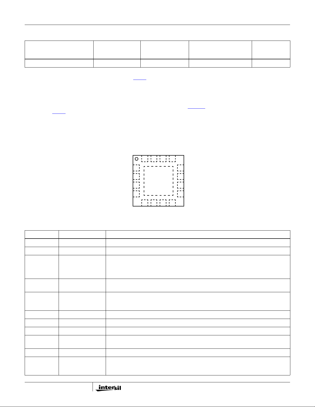
Pin Configuration
ISL8013
(16 LD QFN)
TOP VIEW
NC
LX
LX
LX
15
16 14 13
VIN
VIN
VDD
SYNCH
1
2
3
4
6578
EN
NC
PG
VFB
12
11
10
9
PGND
PGND
SGND
SGND
Pin Descriptions
PIN NUMBER PIN NAME DESCRIPTION
1, 2 VIN Input supply voltage. Connect a 10µF ceramic capacitor to power ground.
3 VDD Input supply voltage for the analog circuitry. Connect to VIN pin.
5 EN Regulator enable pin. Keep the EN voltage low in disabled state until VIN settles or is
above 2.5V. Enable the output when driven to high. Shut down the chip and discharge
output capacitor when driven to low. Do not connect directly to VIN or leave this pin
floating.
7 PG 1ms timer output. At power-up or EN HI, this output is a 1ms delayed Power-Good signal
for the output voltage.
4 SYNCH Mode Selection pin. Connect to logic high or input voltage VDD for PWM mode. Connect
to logic low or ground for PFM mode. Connect to an external function generator for
synchronization with the negative edge trigger. Do not leave this pin floating.
13, 14, 15 LX Switching node connection. Connect to one terminal of the inductor.
11, 12 PGND Power ground
9, 10 SGND Signal ground.
8 VFB Buck regulator output feedback. Connect to the output through a resistor divider for
adjustable output voltage. For 0.8V output voltage, connect this pin to the output.
6, 16 NC No connect.
- Exposed Pad The exposed pad must be connected to the SGND pin for proper electrical performance.
Place as much vias as possible under the pad connecting to SGND plane for optimal
thermal performance.
2
November 23, 2009
FN6309.3
Page 3
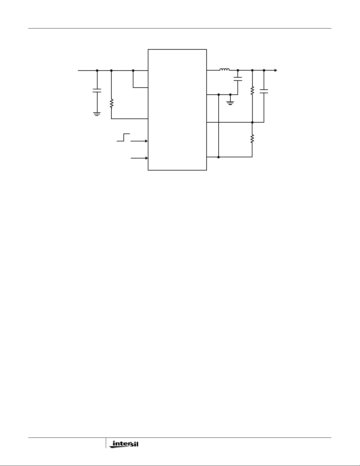
Typical Application
ISL8013
INPUT 2.7V TO 5.5V
C1
2 x 22µF
L
1.5µH
2 x 22µF
R1
100k
VIN
VDD
PG
EN
SYNCH
LX
PGND
ISL8013
VFB
SGND
FIGURE 1. TYPICAL APPLICATION DIAGRAM
C2
R2
124k
R3
100k
OUTPUT
1.8V
C3
47pF
3
November 23, 2009
FN6309.3
Page 4
Block Diagram
SHUTDOWN
EN
BANDGAP
VFB
6k
PG
SGND
SOFT-
Soft
START
0.8V
3pF
0.736V
+
EAMP
-
+
-
1ms
DELAY
+
SLOPE
Slope
COMP
ISL8013
27pF
390k
OSCILLATOR
+
COMP
CONTROLLER
PROTECTION
+
OCP
-
+
SKIP
-
SYNCH
SHUTDOWN
PWM/PFM
LOGIC
DRIVER
CSA
1.4V
0.5V
ZERO-CROSS
SENSING
VIN
LX
PGND
++
-
-
0.2V
SCP
+
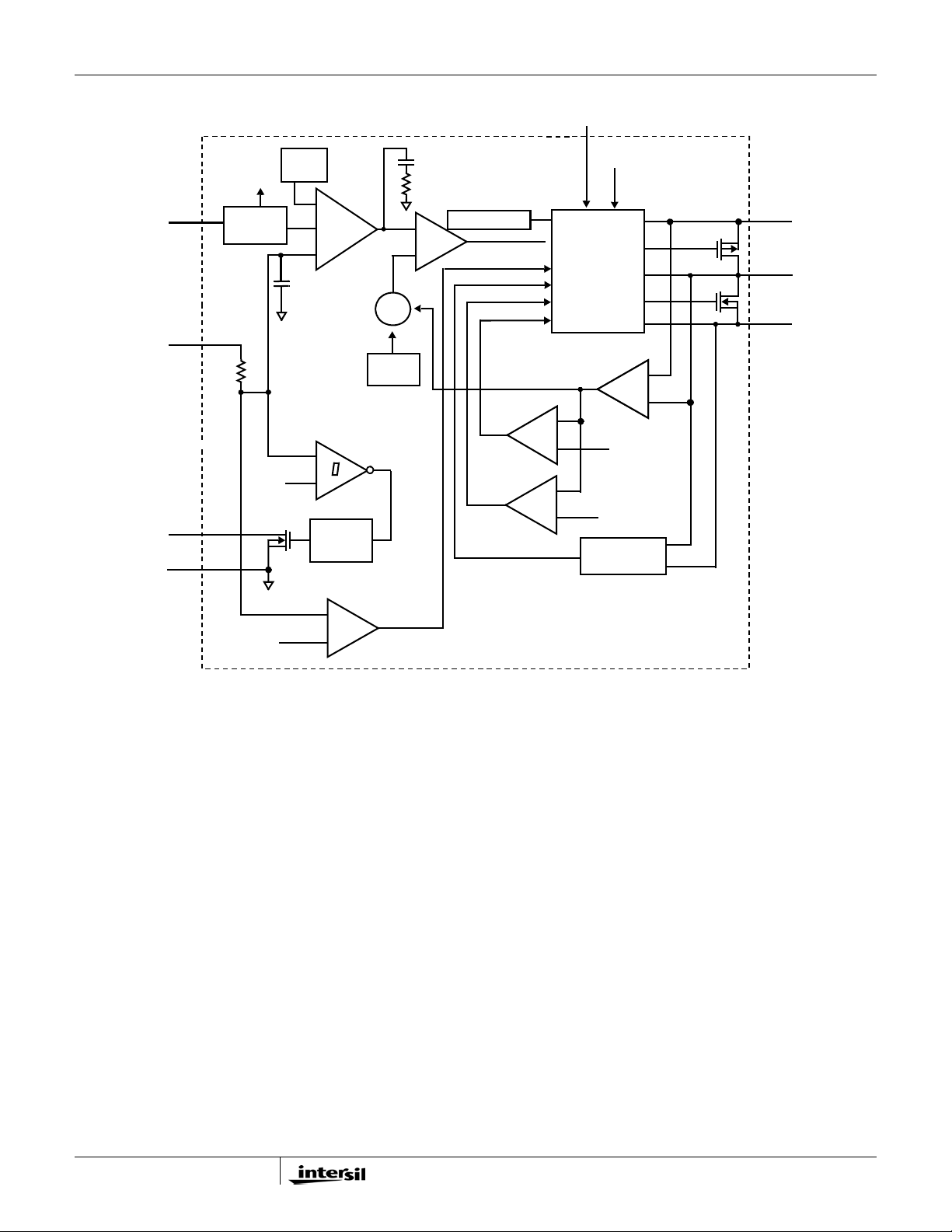
FIGURE 2. FUNCTIONAL BLOCK DIAGRAM
4
November 23, 2009
FN6309.3
Page 5
ISL8013
Absolute Maximum Ratings (Reference to GND) Thermal Information
VIN, VDD . . . . . . . . . . . . . . - 0.3V to 6V (DC) or 7V (20ms)
EN, SYNCH, PG . . . . . . . . . . . . . . . . . .-0.3V to VIN + 0.3V
LX . . . -1.5V (100ns)/-0.3V (DC) to 6.5V (DC) or 7V (20ms)
VFB . . . . . . . . . . . . . . . . . . . . . . . . . . . . . . -0.3V to 2.7V
Recommended Operating Conditions
VIN Supply Voltage Range. . . . . . . . . . . . . . . . 2.7V to 5.5V
Load Current Range . . . . . . . . . . . . . . . . . . . . . . .0A to 3A
Ambient Temperature Range . . . . . . . . . . . .-40°C to +85°C
CAUTION: Do not operate at or near the maximum ratings listed for extended periods of time. Exposure to such conditions may adversely impact
product reliability and result in failures not covered by warranty.
NOTES:
is measured in free air with the component mounted on a high effective th ermal conductivity test board with “direct attach”
4. θ
JA
features. See Tech Brief TB379.
, “case temperature” location is at the c enter of the exposed metal pad on the package underside. See Tech Brief TB379.
5. θ
JC
Thermal Resistance (Typical, Notes 4, 5))θ
(°C/W)θJC (°C/W)
JA
16 Ld 4x4 QFN Package . . . . . . . 39 3
Junction Temperature Range . . . . . . . . . . -55°C to +125°C
Storage Temperature Range. . . . . . . . . . . -65°C to +150°C
Pb-Free Reflow Profile . . . . . . . . . . . . . . . . . .see link below
http://www.intersil.com/pbfree/Pb-FreeReflow.asp
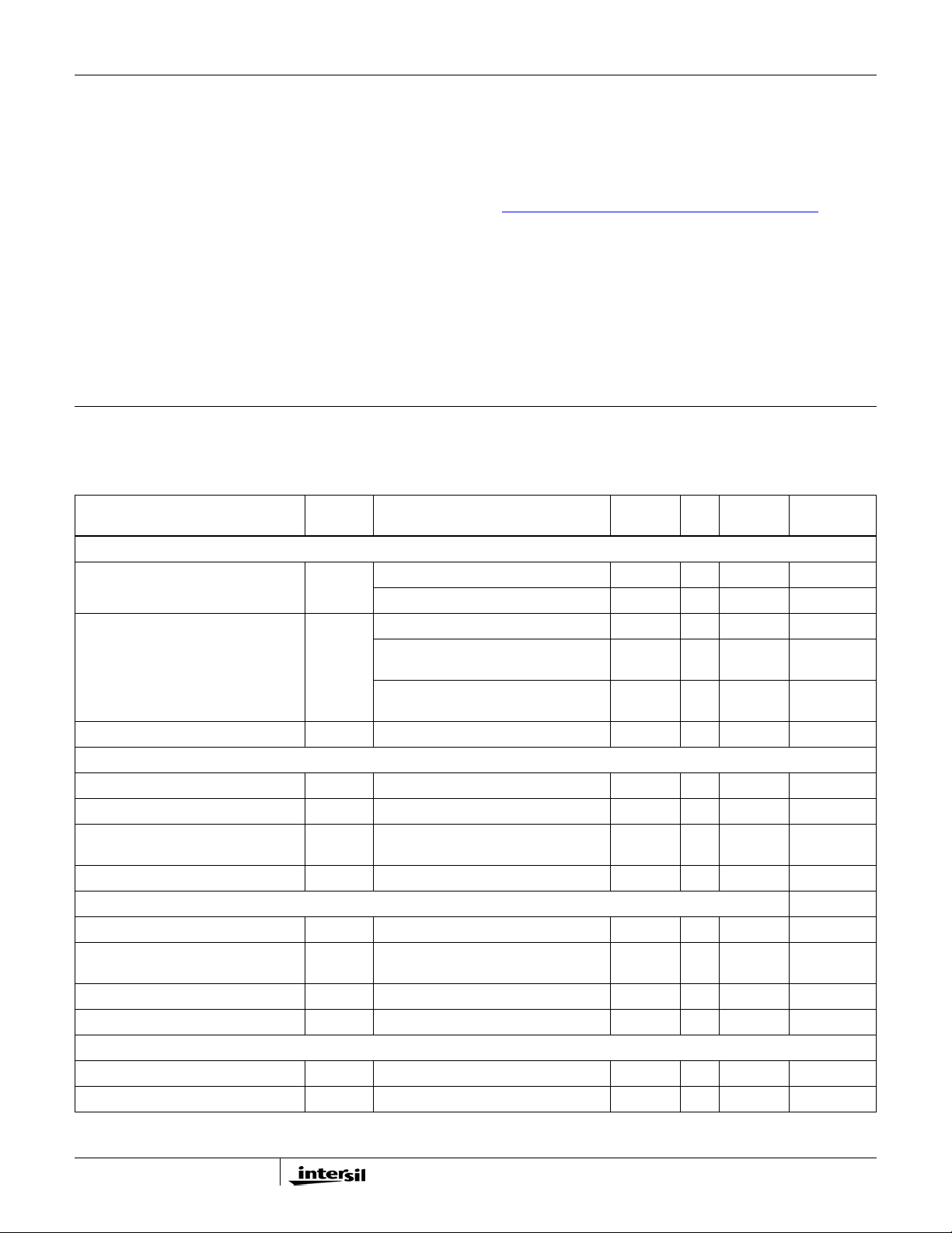
Electrical Specifications Unless otherwise noted, all parameter limits are established over the recommended
operating conditions and the typical specification are measured at the following conditions:
T
= -40°C to +85°C, VIN = 3.6V, EN = VDD, unless otherwise noted. Typical values are at
A
T
= +25°C. Boldface limits apply over the operating temperature range, -40°C to
A
+85°C.
MIN
PARAMETER SYMBOL TEST CONDITIONS
(Note 7) TYP
INPUT SUPPLY
Undervoltage Lockout Threshold V
V
IN
UVLO
Rising, no load - 2.5 2.7 V
Falling, no load 2.2 2.4 - V
Quiescent Supply Current I
SYNCH = GND, no load at the output - 35 - µA
VIN
SYNCH = GND, no load at the output
- 30 45 µA
and no switches switching
Shut Down Supply Current I
SYNCH = VDD, F
at the output
VIN = 5.5V, EN = low - 0.1 2 µA
SD
= 1MHz, no load
S
- 6.5 10 mA
OUTPUT REGULATION
Reference Voltage V
VFB Bias Current I
REF
VFB
Line Regulation V
VFB = 0.75V - 0.1 - µA
= VO + 0.5V to 5.5V (minimal
IN
0.790 0.8 0.810 V
- 0.2 - %/V
2.7V)
Soft-Start Ramp Time Cycle - 1 - ms
OVERCURRENT PROTECTION
Current Limit Blanking Time t
Overcurrent and Auto Restart
OCON
t
OCOFF
- 17 - Clock pulses
- 4 - SS cycle
Period
Switch Current Limit I
Peak Skip Limit I
LIMIT
SKIP
(Note 6) 4.0 4.8 5.9 A
(Note 6) - 1.2 - A
COMPENSATION
Error Amplifier Trans-Conductance - 20 - µA/V
Trans-Resistance RT 0.213 0.25 0.287 Ω
MAX
(Note 7) UNITS
5
November 23, 2009
FN6309.3
Page 6
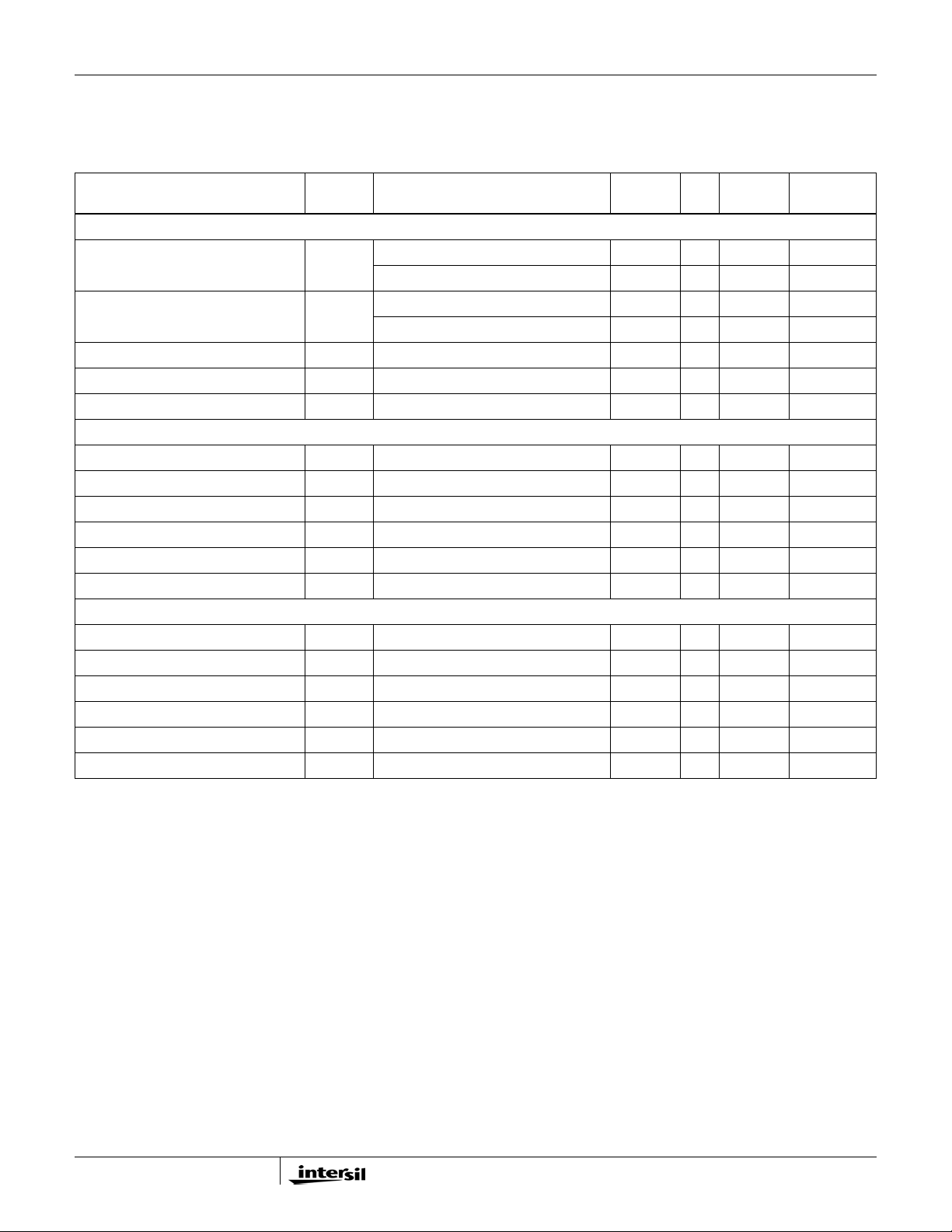
ISL8013
Electrical Specifications Unless otherwise noted, all parameter limits are established over the recommended
operating conditions and the typical specification are measured at the following conditions:
T
= -40°C to +85°C, VIN = 3.6V, EN = VDD, unless otherwise noted. Typical values are at
A
T
= +25°C. Boldface limits apply over the operating temperature range, -40°C to
A
+85°C. (Continued)
MIN
PARAMETER SYMBOL TEST CONDITIONS
(Note 7) TYP
LX
P-Channel MOSFET ON-Resistance V
N-Channel MOSFET ON-Resistance V
= 5V, IO = 200mA - 50 75 mΩ
IN
= 2.7V, IO = 200mA - 70 100 mΩ
V
IN
= 5V, IO = 200mA - 50 75 mΩ
IN
= 2.7V, IO = 200mA - 70 100 mΩ
V
IN
LX Maximum Duty Cycle - 100 - %
PWM Switching Frequency f
S
0.80 1.00 1.20 MHz
LX Minimum On-Time SYNCH = High - - 140 ns
PG
Output Low Voltage Sinking 1mA - - 0.3 V
Delay Time (Rising Edge) 0.65 1 1.35 ms
PG Pin Leakage Current PG = VIN = 3.6V - 0.01 0.1 µA
PGOOD Rising Threshold Percentage of regulation voltage 89 92 95 %
PGOOD Falling Threshold Percentage of regulation voltage 85 88 91.5 %
PGOOD Delay Time (Falling Edge) - 15 - µs
EN, SYNCH
Logic Input Low - - 0.4 V
Logic Input High 1.4 - - V
Synch Logic Input Leakage Current I
Enable Logic Input Leakage Current I
SYNCH
Pulled up to 5.5V - 0.1 1 μA
EN
- 0.1 1 μA
Thermal Shutdown - 140 - °C
Thermal Shutdown Hysteresis - 25 - °C
NOTES:
6. Limits established by characterization and are not production tested.
7. Parameters with MIN and/or MAX limits are 100% tested at +25°C, unless otherwise specified. T emperature limits established
by characterization and are not production tested.
MAX
(Note 7) UNITS
6
November 23, 2009
FN6309.3
Page 7
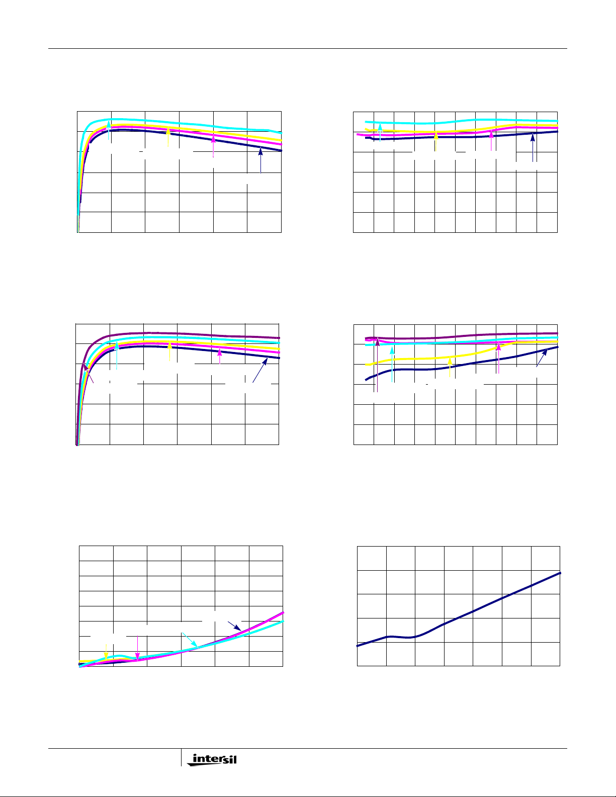
ISL8013
0
Typical Operating Performance (Unless otherwise not ed, oper ating co nditions are: T
= 2.5V to 5.5V, EN = VIN, SYNCH = 0V, L = 1.5µH,
V
VIN
100
90
2.5V
80
70
60
EFFICIENCY (%)
50
40
0.0 0.5 1.0 1.5 2.0 2.5 3.0
OUT-PWM
1.8V
OUT-PWM
1.5V
OUTPUT LOAD (A)
OUT-PWM
1.2V
OUT-PWM
FIGURE 3. EFFICIENCY vs LOAD (1MHz 3.3 VIN PWM)
100
90
= 2x22µF, C2 = 2x22µF, I
C
1
100
90
2.5V
80
70
60
EFFICIENCY (%)
50
40
OUT-PFM
0.0 0.1 0.2 0.3 0.4 0.5 0.6 0.7 0.8 0.9 1.0
FIGURE 4. EFFICIENCY vs LOAD (1MHz 3.3 V
100
90
= 0A to 3A).
OUT
1.8V
OUT-PFM
OUTPUT LOAD (A)
1.5V
OUT-PFM
1.2V
= +25°C,
A
OUT-PFM
PFM)
IN
80
70
60
EFFICIENCY (%)
50
40
2.5V
3.3V
OUT-PWM
0.0 0.5 1.0 1.5 2.0 2.5 3.0
FIGURE 5. EFFICIENCY vs LOAD (
2.00
1.75
1.50
1.25
1.00
0.75
0.50
0.25
POWER DISSIPATION (W)
0.00
5V
IN-PWM
0.0 0.5 1.0 1.5 2.0 2.5 3.
1.8V
OUT-PWM
OUTPUT LOAD (A)
.
3
V
3
-
N
P
I
OUTPUT LOAD (A)
OUT-PWM
5V
F
M
IN-PFM
1.5V
OUT-PWM
1.2V
OUT-PWM
1MHz 5VIN PWM)
3.3V
IN-PWM
FIGURE 7. POWER DISSIPATION vs LOAD (1MHz,
= 1.8V)
V
OUT
80
70
60
EFFICIENCY (%)
50
40
2.5V
3.3V
0.0 0.1 0.2 0.3 0.4 0.5 0.6 0.7 0.8 0.9 1.0
OUT-PFM
OUT-PFM
1.8VOUT-PFM
OUTPUT LOAD (A)
FIGURE 6. EFFICIENCY vs LOAD (
125
100
75
50
25
POWER DISSIPATION (mW)
0
2.0 2.5 3.0 3.5 4.0 4.5 5.0 5.5
(V)
V
IN
1.2V
OUT-PFM
OUT-PFM
1.5V
1MHz 5VIN PFM
)
FIGURE 8. POWER DISSIPATION WITH NO LOAD vs
V
IN
(PWM V
OUT
= 1.8V)
7
November 23, 2009
FN6309.3
Page 8
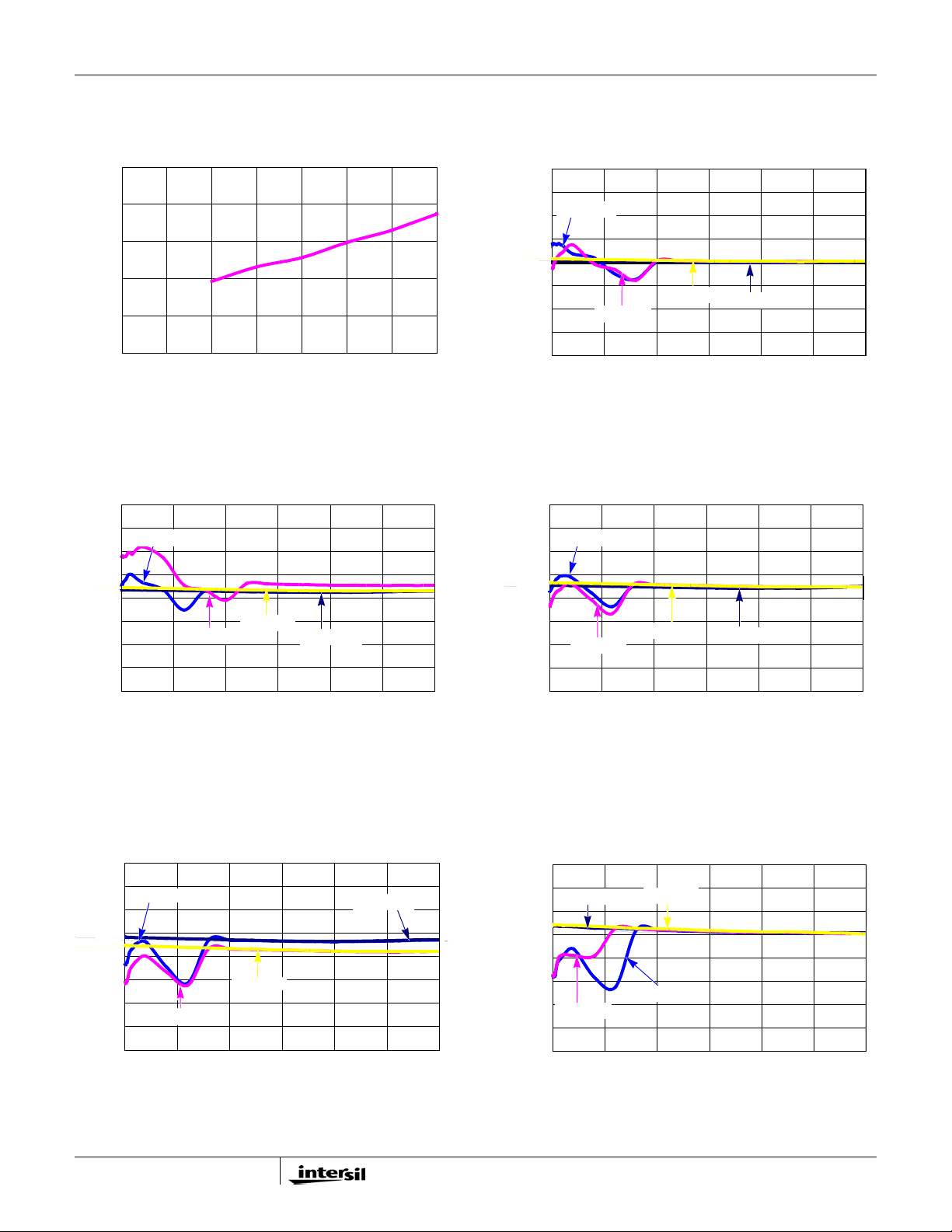
0
0
ISL8013
Typical Operating Performance (Unless otherwise not ed, oper ating co nditions are: T
= 2.5V to 5.5V, EN = VIN, SYNCH = 0V, L = 1.5µH,
V
VIN
0.25
0.20
0.15
0.10
0.05
POWER DISSIPATION (mW)
0
2.0 2.5 3.0 3.5 4.0 4.5 5.0 5.5
(V)
V
IN
FIGURE 9. POWER DISSIPATION WITH NO LOAD vs
V
(PFM V
IN
1.55
1.54
3.3V
1.53
1.52
1.51
1.50
1.49
OUTPUT VOLTAGE (V)
1.48
1.47
FIGURE 11. V
IN-PFM
5V
IN-PFM
0.0 0.5 1.0 1.5 2.0 2.5 3.0
REGULATION vs LOAD (1MHz,
OUT
V
= 1.5V)
OUT
= 1.8V)
OUT
5V
IN-PWM
3.3V
OUTPUT LOAD (A)
IN-PWM
= 2x22µF, C2 = 2x22µF, I
C
1
1.24
1.23
3.3V
1.22
1.21
1.20
1.19
1.18
OUTPUT VOLTAGE (V)
1.17
1.16
FIGURE 10. V
1.83
1.82
1.81
1.80
1.79
1.78
1.77
OUTPUT VOLTAGE (V)
1.76
1.75
FIGURE 12. V
IN-PFM
5V
IN-PFM
0.0 0.5 1.0 1.5 2.0 2.5 3.
OUT
V
OUT
3.3V
IN-PFM
5V
IN-PFM
0.0 0.5 1.0 1.5 2.0 2.5 3.0
OUT
V
OUT
REGULATION vs LOAD (1MHz,
= 1.2V)
REGULATION vs LOAD (1MHz,
= 1.8V)
= 0A to 3A). (Continued)
OUT
5V
IN-PWM
3.3V
IN-PWM
OUTPUT LOAD (A)
5V
IN-PWM
OUTPUT LOAD (A)
3.3V
IN-PWM
= +25°C,
A
2.52
2.51
3.3V
2.50
2.49
2.48
2.47
2.46
OUTPUT VOLTAGE (V)
2.45
2.44
FIGURE 13. V
IN-PFM
5V
IN-PWM
5V
IN-PFM
0.0 0.5 1.0 1.5 2.0 2.5 3.0
OUT
V
OUT
OUTPUT LOAD (A)
REGULATION vs LOAD (1MHz,
= 2.5V)
3.3V
8
IN-PWM
3.36
3.35
4.5V
3.34
3.33
3.32
3.31
3.30
OUTPUT VOLTAGE (V)
3.29
3.28
IN-PWM
5V
IN-PFM
0.0 0.5 1.0 1.5 2.0 2.5 3.
FIGURE 14. V
V
OUT
5V
IN-PWM
4.5V
IN-PFM
OUTPUT LOAD (A)
REGULATION vs LOAD (1MHz,
OUT
= 3.3V)
November 23, 2009
FN6309.3
Page 9
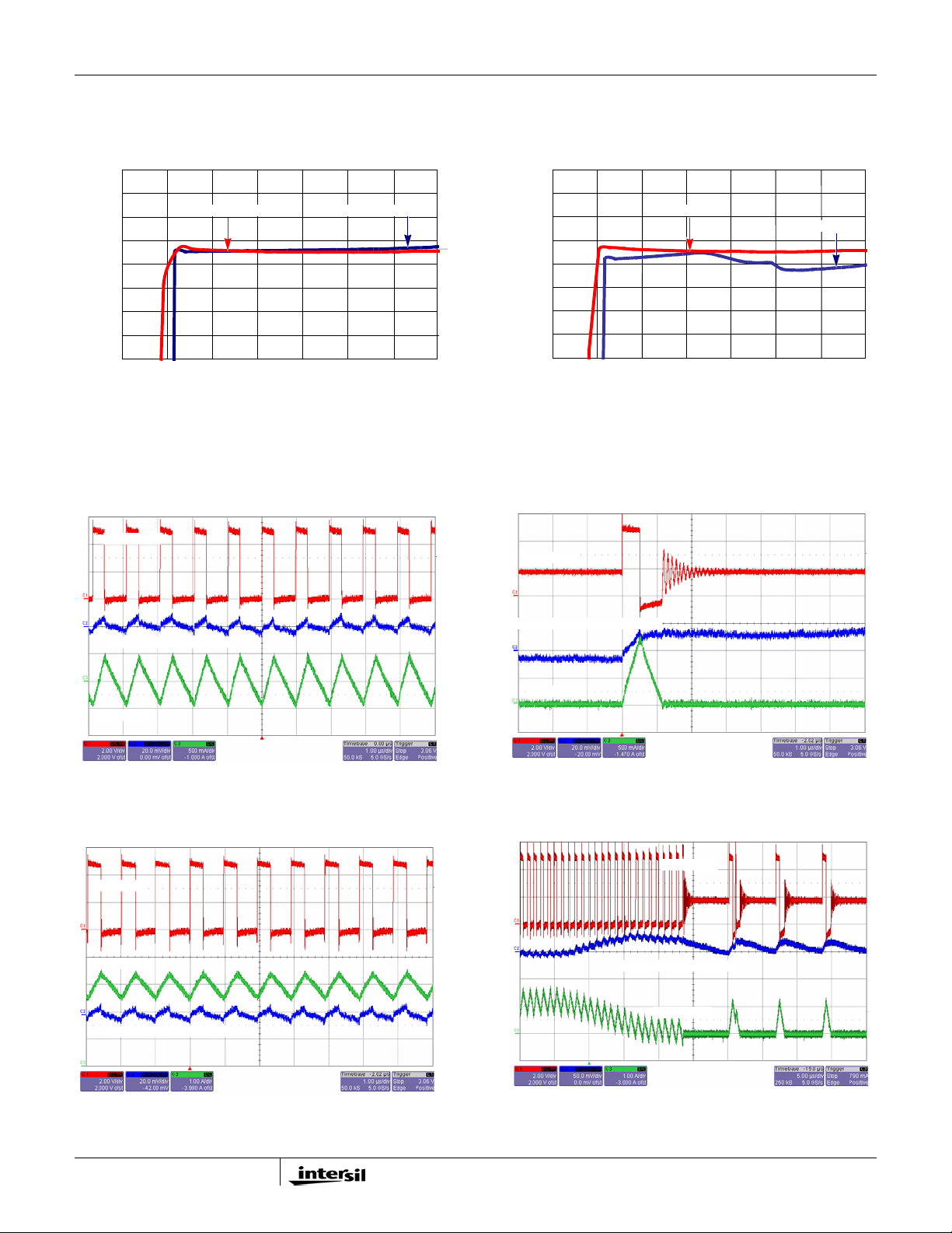
OUTPUT VOLTAGE (V)
5
5
ISL8013
Typical Operating Performance (Unless otherwise not ed, oper ating co nditions are: T
= 2.5V to 5.5V, EN = VIN, SYNCH = 0V, L = 1.5µH,
V
VIN
1.830
1.820
1.810
1.800
1.790
1.780
1.770
1.760
1.750
2.02.53.03.54.04.55.05.
3A LOAD PWM
INPUT VOLTAGE (V)
0A LOAD PWM
FIGURE 15. OUTPUT VOLTAGE RE GULATION vs VIN
(PWM V
LX 2V/DIV
OUT
= 1.8 )
= 2x22µF, C2 = 2x22µF, I
C
1
1.830
1.820
1.810
1.800
1.790
1.780
1.770
OUTPUT VOLTAGE (V)
1.760
1.750
2.0 2.5 3.0 3.5 4.0 4.5 5.0 5.
FIGURE 16. OUTPUT VOLTAGE REGULATION vs V
(PFM V
LX 2V/DIV
= 0A to 3A). (Continued)
OUT
3A LOAD
INPUT VOLTAGE (V)
= 1.8V)
OUT
= +25°C,
A
0A LOAD
IN
RIPPLE 20mV/DIV
V
OUT
IL 0.5A/DIV
FIGURE 17. STEADY STATE OPERATION AT NO LOAD
(PWM)
LX 2V/DIV
IL 1A/DIV
V
RIPPLE 20mV/DIV
OUT
V
RIPPLE 20mV/DIV
OUT
IL 0.5A/DIV
FIGURE 18. STEADY STATE OPERATION AT NO LOAD
(PFM)
LX 2V/DIV
RIPPLE 50mV/DIV
V
OUT
IL 1A/DIV
FIGURE 19. STEADY STATE OPERAT ION WITH FULL
LOAD
9
FIGURE 20. MODE TRANSITION CCM TO DCM
November 23, 2009
FN6309.3
Page 10
ISL8013
Typical Operating Performance (Unless otherwise not ed, oper ating co nditions are: T
= 2.5V to 5.5V, EN = VIN, SYNCH = 0V, L = 1.5µH,
V
VIN
LX 2V/DIV
RIPPLE 50mV/DIV
V
OUT
IL 1A/DIV
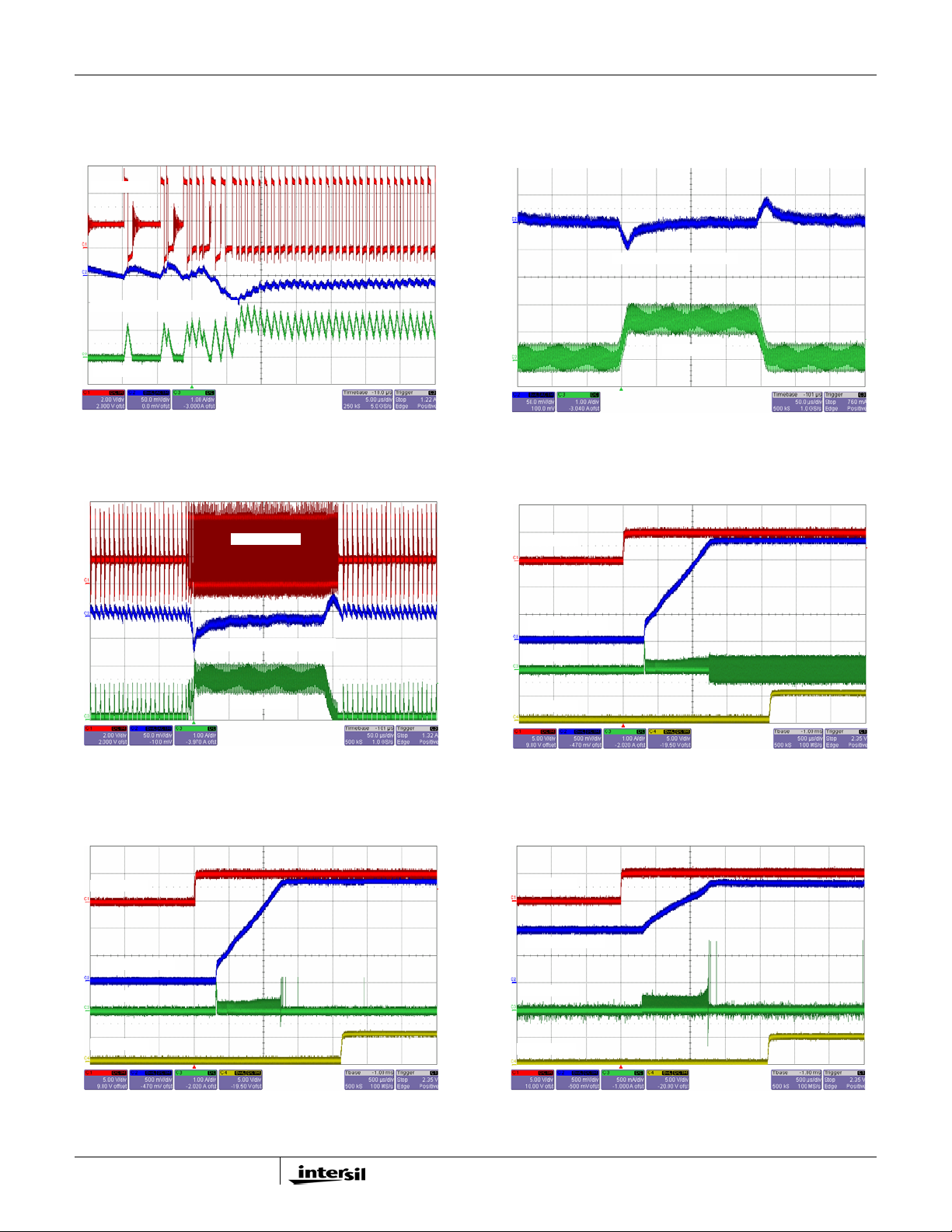
FIGURE 21. MODE TRANSITION DCM TO CCM
LX 2V/DIV
= 2x22µF, C2 = 2x22µF, I
C
1
V
FIGURE 22. LOAD TRANSIENT (PWM)
EN 5V/DIV
OUT
= 0A to 3A). (Continued)
OUT
RIPPLE 50mV/DIV
IL 1A/DIV
= +25°C,
A
RIPPLE 50mV/DIV
V
OUT
IL 1A/DIV
FIGURE 23. LOAD TRANSIENT (PFM)
EN 5V/DIV
V
0.5V/DIV
OUT
IL 1A/DIV
PG 5V/DIV
0.5V/DIV
V
OUT
IL 1A/DIV
PG 5V/DIV
FIGURE 24. SOFT-START WITH NO LOAD (PWM)
EN 5V/DIV
V
0.5V/DIV
OUT
IL 5A/DIV
PG 5V/DIV
FIGURE 25. SOFT-START AT NO LOAD (PFM)
10
FIGURE 26. SOFT-START WITH PRE-BIASED 1V
November 23, 2009
FN6309.3
Page 11
ISL8013
Typical Operating Performance (Unless otherwise not ed, oper ating co nditions are: T
= 2.5V to 5.5V, EN = VIN, SYNCH = 0V, L = 1.5µH,
V
VIN
= 2x22µF, C2 = 2x22µF, I
C
1
EN 5V/DIV
V
0.5V/DIV
OUT
IL 1A/DIV
PG 5V/DIV
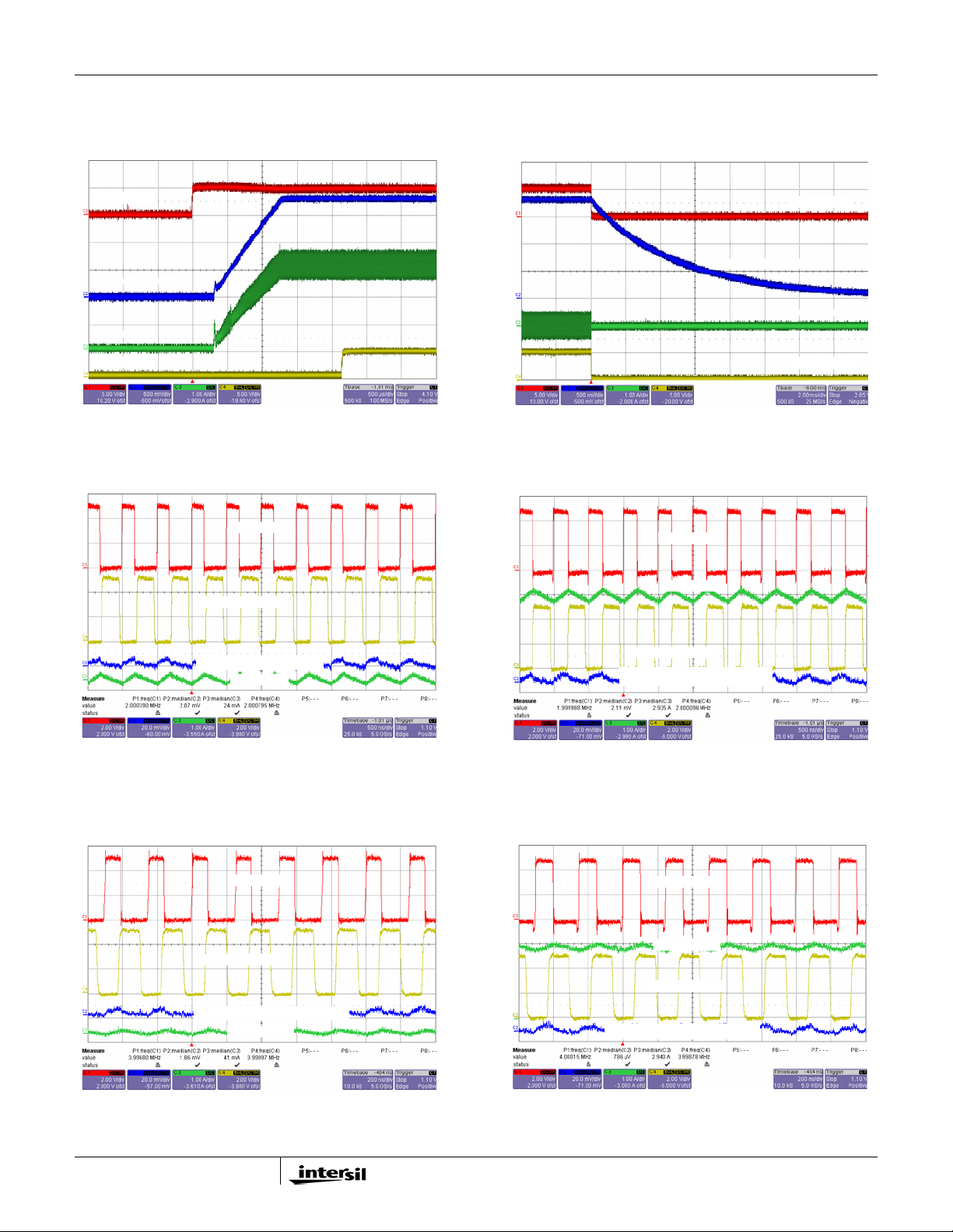
FIGURE 27. SOFT-START AT FULL LOAD FIGURE 28. SOFT-DISCHARGE SHUTDOWN
LX 2V/DIV
= 0A to 3A). (Continued)
OUT
V
0.5V/DIV
OUT
LX 2V/DIV
= +25°C,
A
EN 5V/DIV
IL 1A/DIV
PG 5V/DIV
SYNCH 2V/DIV
V
RIPPLE 20mV/DIV
OUT
IL 1A/DIV
FIGURE 29. STEADY STATE OPERATION AT NO LOAD
WITH FREQUENCY = 2MHz
LX 2V/DIV
SYNCH 2V/DIV
V
RIPPLE 20mV/DIV
OUT
IL 1A/DIV
IL 1A/DIV
SYNCH 2V/DIV
V
RIPPLE 20mV/DIV
OUT
FIGURE 30. STEADY STATE OPERATION AT FULL
LOAD WITH FREQUENCY = 2MHz
LX 2V/DIV
IL 1A/DIV
SYNCH 2V/DIV
V
RIPPLE 20mV/DIV
OUT
FIGURE 31. STEADY STATE OPERATION AT NO LOAD
WITH FREQUENCY = 4MHz
11
FIGURE 32. STEADY STATE OPERATION AT FULL
LOAD (PWM) WITH FREQUENCY = 4MHz
November 23, 2009
FN6309.3
Page 12
ISL8013
Typical Operating Performance (Unless otherwise not ed, oper ating co nditions are: T
= 2.5V to 5.5V, EN = VIN, SYNCH = 0V, L = 1.5µH,
V
VIN
PHASE 2V/DIV
V
OUT
IL 2A/DIV
PG 5V/DIV
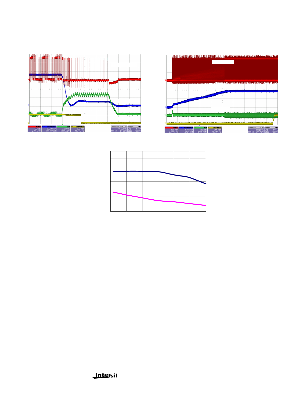
FIGURE 33. OUTPUT SHORT CIRCUIT
5.000
4.875
4.750
4.625
4.500
4.375
4.250
OUTPUT CURRENT (A)
4.125
4.000
-50-250 255075100
0.5V/DIV
= 2x22µF, C2 = 2x22µF, I
C
1
FIGURE 34. OUTPUT SHORT CIRCUIT RECOVERY
OCP_3.3V
OCP_5V
TEMPERATURE (°C)
IN
IN
= 0A to 3A). (Continued)
OUT
LX 2V/DIV
V
1V/DIV
OUT
IL 2A/DIV
PG 5V/DIV
= +25°C,
A
FIGURE 35. OUTPUT CURRENT LIMIT vs TEMPERATURE
Theory of Operation
The ISL8013 is a step-down switching regulator
optimized for battery-powered handheld applications.
The regulator operates at 1MHz fixed switching
frequency under heavy load conditions to allow smaller
external inductors and capacitors to be used for minimal
printed-circuit board (PCB) area. At light load, the
regulator reduces the switching frequency , unless forced
to the fixed frequency , to minimize the switching loss and
to maximize the battery life. The quiescent current when
the output is not loaded is typically only 35µA. The
supply current is typically only 0.1µA when the regulator
is shut down.
PWM Control Scheme
Pulling the SYNCH pin HI (>2.5V) forces the converter
into PWM mode, regardless of output current. The
ISL8013 employs the current-mode pulse-width
modulation (PWM) control scheme for fast transient
response and pulse-by-pulse current limiting. Figure 2
shows the block diagram. The current loop consists of the
oscillator, the PWM comparator, current sensing circuit
and the slope compensation for the current loop stability .
The gain for the current sensing circuit is typically
250mV/A. The control reference for the current loops
comes from the error amplifier's (EAMP) output.
The PWM operation is initialize d by the cloc k from the
oscillator. The P-Channel MOSF ET is turned on at the
beginning of a PWM cycle and the current in the
MOSFET starts to ramp up. When the sum of the current
amplifier CSA and the slope compensation (237mV/µs)
reaches the control reference of the current loop, the
PWM comparator COMP sends a sign al to the PWM logic
to turn off the P-MOSFET and turn on the N-Channel
MOSFET. The N-MOSFET stays on until the end of the
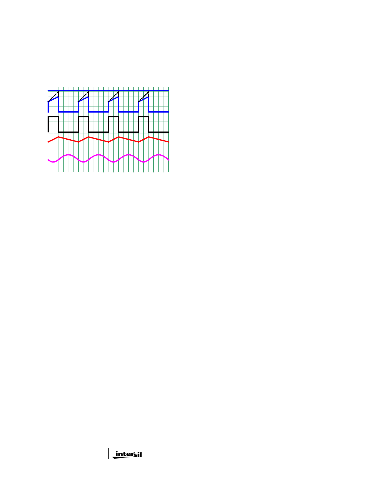
PWM cycle. Figure 36 shows the typical operating
waveforms during the PWM operation. The dotted lines
illustrate the sum of the slope compensation r amp a nd
the current-sense amplifier’s CSA output.
The output voltage is regulated by controlling the V
EAMP
voltage to the current loop. The bandgap circuit outputs
a 0.8V reference voltage to the voltage loop. The
feedback signal comes from the VFB pin. The soft-start
12
November 23, 2009
FN6309.3
Page 13
ISL8013
block, only affects the operation during the start-up and
will be discussed separately. The error amplifier is a
transconductance amplifier that converts the voltage
error signal to a current output. The voltage loop is
internally compensated with the 27pF and 390kΩ RC
network. The maximum EAMP voltage output is precisely
clamped to 1.6V.
V
EAMP
V
CSA
DUTY
CYCLE
I
L
V
OUT
FIGURE 36. PWM OPERATION WAVEFORMS
SKIP Mode
Pulling the SYNCH pin LO (<0.4V) forces the converter
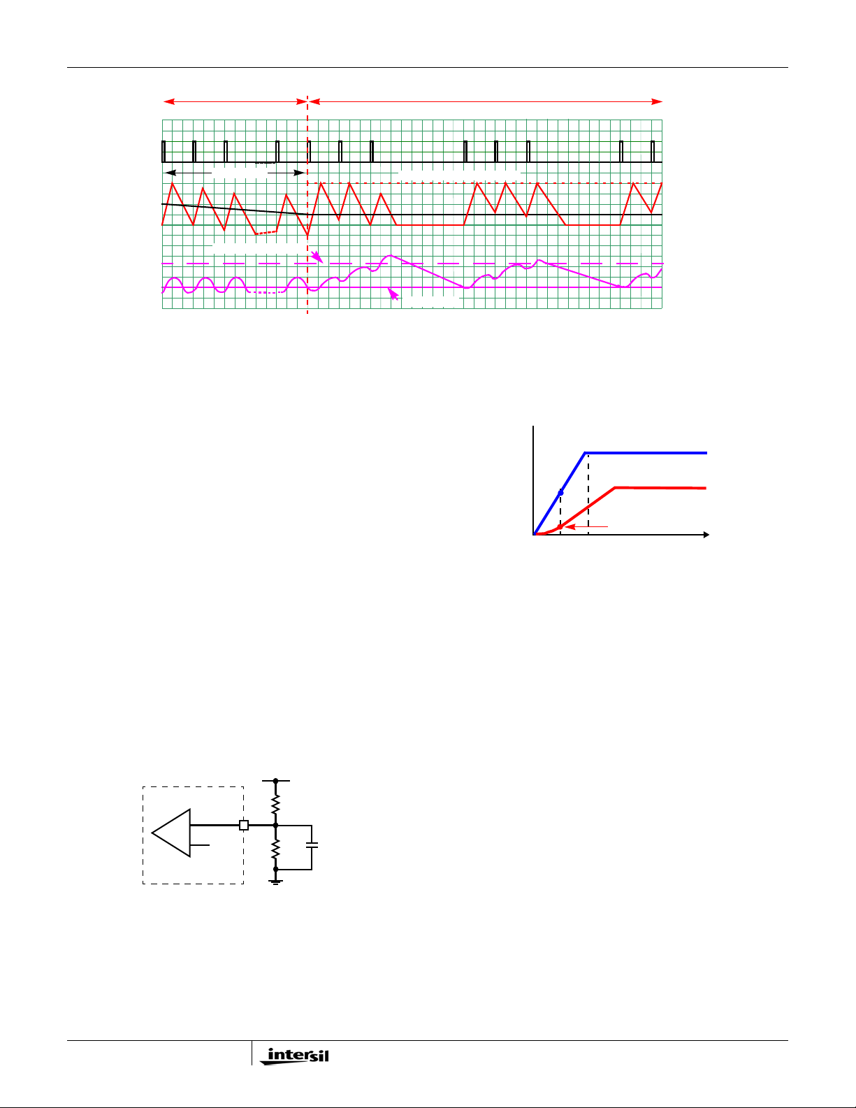
into PFM mode. The ISL8013 enters a pulse-s kipping
mode at light load to minimize the switching loss by
reducing the switching frequency. Figure 37 illustrates
the skip-mode operation. A zero-cross sensing circuit
shown in Figure 2 monitors the N-MOSFET current for
zero crossing. When 8 consecutive cycles of the inductor
current crossing zero are detected, the regulator enters
the skip mode. During the eight detecting cycles, the
current in the inductor is allowed to become negative.
The counter is reset to zero when the current in any cycle
does not cross zero.
Once the skip mode is entered, the pulse modulation
starts being controlled by the SKIP comparator shown in
Figure 2. Each pulse cycle is still synchronized by the
PWM clock. The P-MOSFET is turned on at the clock's
rising edge and turned off when the output is higher than
1.5% of the nominal regulation or when its current
reaches the peak Skip current limit value. Then the
inductor current is discharging to 0A and stays at zero.
The internal clock is disabled.The output voltage reduces
gradually due to the load current discharging the output
capacitor. When the output voltage drops to the nominal
voltage, the P-MOSFET will be turned on again at the
rising edge of the internal clock as it repeats the previous
operations.
The regulator resumes normal PWM mode operation
when the output voltage drops 1.5% b elow the nominal
voltage.
Synchronization Control
The frequency of operation can be synchronized up to
4MHz by an external signal applied to the SYNCH pin.
The falling edge on the SYNCH triggers the rising edge of
the LX pulse. Make sure that the minimum on time of the
LX node is greater than 140ns.
Overcurrent Protection
The overcurrent protection is realized by monitoring the
CSA output with the OCP comparator, as shown in
Figure 2. The current sensing circuit has a gain of
250mV/A, from the P-MOSFET current to the CSA
output. When the CSA output reaches 1.4V, which is
equivalent to 4.8A for the swit ch cu rrent, th e OC P
comparator is tripped to turn off t he P-MOSFET
immediately. The overcurrent function protects the
switching converter from a shorted outpu t by
monitoring the current flow in g thro ugh t he upper
MOSFET.
Upon detection of overcurrent condition, the upper
MOSFET will be immediately turned off and will not be
turned on again until the next switching cycle. Upon
detection of the initial overcurrent condition, the
overcurrent fault counter is set to 1. If , on the
subsequent cycle, another overcurrent condition is
detected, the OC fault counter will be incremented. If
there are 17 sequential OC fault detections, the regulator
will be shut down under an overcurrent fault condition .
An overcurrent fault condition will result in the regulator
attempting to restart in a hiccup mode within the delay of
four soft-start periods. At the end of the fourth soft-start
wait period, the fault counters are reset and soft-start is
attempted again. If the overcurrent condition goes away
during the delay of four soft-start periods, the output will
resume back into regulation point after hiccup mode
expires.
Short-Circuit Protection
The short-circuit protection SCP comparator monitors the
VFB pin voltage for output short-circuit protection. When
the VFB is lower than 0.2V, the SCP comparator forces
the PWM oscillator frequency to drop to 1/3 of the normal
operation value. This comparator is effective during
start-up or an output short-circuit event.
13
November 23, 2009
FN6309.3
Page 14
ISL8013
.
CLOCK
I
L
0
V
OUT
PWM
8 CYCLES
NOMINAL +1.5%
FIGURE 37. SKIP MODE OPERATION WAVEFORMS
PFM CURRENT LIMIT
PG
During power-up, the open-drain power good output
holds low for about 1ms after V
reaches the
OUT
regulation voltage. The PG output also serves as a 1ms
delayed the Power Good signal when the pull-up resistor
is installed.
R
1
Soft Start-Up
The soft-start-up reduces the inrush current during the
start-up. The soft-start block outputs a ramp reference to
the input of the error amplifier. This voltage ramp limits
the inductor current as well as the output voltage speed
so that the output voltage rises in a controlled fashion.
When VFB is less than 0.2V at the beginning of the softstart, the switching frequency is reduced to 1/3 of the
nominal value so that the output can start-up smoothly
at light load condition. During soft-start, the IC operates
in the SKIP mode to support pre-biased output condition.
UVLO
When the input voltage is below the undervol tage
lock-out (UVLO) threshold, the regulator is disabled. To
adjust the voltage level of power on and UVLO, use a
resistive divider across EN. The input voltage
programming resistor R
resistor R
, as referred to in Figure 38. The value of R5 is
5
will depend on the bottom
4
typically between 10kΩ and 100kΩ.
V
IN
EN
+
1V
-
FIGURE 38. EXTERNAL RESISTOR DIVIDER
R4
R5
C
Enable
The enable (EN) input allows the user to control the
turning on or off the regulator for purposes such as
power-up sequencing. When the regulator is enabled,
there is typically a 600µs delay for waking up the
PFM
LOAD CURRENTT
NOMINAL
bandgap reference and then the soft-start-up begins. It
is recommended that the EN voltage should be kept logic
low (less than 400mV), until V
reaches 2.5V. Refer to
IN
Figures 38 and 39 for suggested circuit implementation
with V
FIGURE 39. CIRCUIT IMPLEMENTATION WITH VIN
slew rate.
IN
2.5V
V (VOLTS)
SLEW RATE
T
VIN
EN
<400mV
t (TIME)
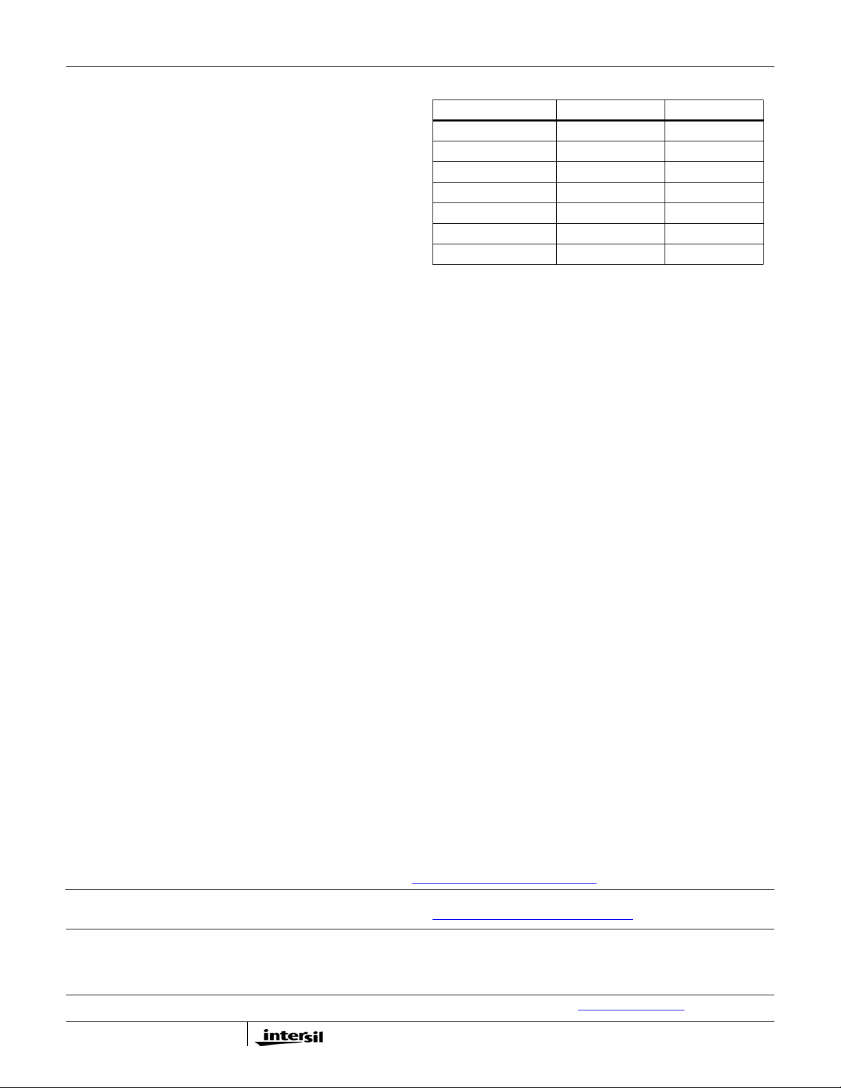
Let T equal the rise time of VIN. Select the ratio of R5 and
such that the voltage is 1.4V (minimum enable logic
R
4
high threshold) when VIN is equal to or greater than
2.5V . Set R5 between 10kΩ to 100kΩ, and use Equation 1
to determine R
R5VIN1.4V–()⋅
---------------------------------------------
=
R
4
Where V
IN
:
4
1.4V
is greater than or equal to 2.5V.
Then select C such that the equivalent time constant is at
least 2x the rise time, T. This will delay the EN voltage
enough so that the overall EN voltage is less than 400mV
by the time V
2T•
--------------------
≥
C
||
R
4R5
Where T is the rise time of V
As an example, let V
Then R
4
reaches 2.5V. Use Equation 2 to get C:
IN
IN
= 5V with rise time, T = 10ms.
IN
= 56.2kΩ, R5 = 71.5kΩ, and C = 0.68µF are
used to insure that VIN was >2.5V and the EN voltage
was <400mV.
Discharge Mode (Soft-Stop)
When a transition to shutdown mode occurs or the VIN
UVLO is set, the outputs discharge to GND through an
internal 100Ω switch.
(EQ. 1)
(EQ. 2)
14
November 23, 2009
FN6309.3
Page 15
ISL8013
Power MOSFETs
The power MOSFET s are optimized for best efficiency.
The ON-resistance for the P-MOSFET is typically 50mΩ
and the ON-resistance for the N-MOSFET is typically
50mΩ.
100% Duty Cycle
The ISL8013 features 100% duty cycle operation to
maximize the battery life. When the battery voltage
drops to a level that the ISL8013 can no longer maintain
the regulation at the output, the regulator completely
turns on the P-MOSFET. The maximum dropout voltage
under the 100% duty-cycle operation is the product of
the load current and the ON-resistance of the P-MOSFET.
Thermal Shut-Down
The ISL8013 has built-in thermal protection. When the
internal temperature reaches +140°C, the regulator is
completely shut down. As the temperature drops to
+115°C, the ISL8013 resumes operation by stepping
through the soft-start.
Applications Information
Output Inductor and Capacitor Selection
To consider steady state and transient operations,
ISL8013 typically uses a 1.5µH output inductor . The
higher or lower inductor value can be used to optimize
the total converter system performance. For example, for
higher output voltage 3.3V application, in order to
decrease the inductor current ripple and output voltage
ripple, the output inductor value can be increased. It is
recommended to set the ripple inductor current
approximately 30% of the maximum output current for
optimized performance. The inductor ripple current can
be expressed as shown in Equation 3:
V
⎛⎞
O
V
-------------------------------------
ΔI
=
The inductor’s saturation current rating needs to be at
least larger than the peak current. The ISL8013 protects
the typical peak current 4.8A. The saturation current
needs be over 5.5A for maximum output current
application.
ISL8013 uses internal compensation network and the
output capacitor value is dependent on the output
voltage. The ceramic capacitor is recommended to be
X5R or X7R. The recommended X5R or X7R
output capacitor values are shown in Table 1.
---------
1
–
⋅
⎜⎟
O
V
⎝⎠
IN
⋅
Lf
S
(EQ. 3)
minimum
TABLE 1. OUTPUT CAPACITOR VALUE vs V
V
(V) C
OUT
0.8 2 x 22 1.0~2.2
1.2 2 x 22 1.0~2.2
1.5 2 x 22 1.5~3.3
1.8 2 x 22 1.5~3.3
2.5 2 x 22 1.5~3.3
3.3 2 x 22 2.2~4.7
3.6 2 x 22 2.2~4.7
(µF) L (µH)
OUT
OUT
In Table 1, the minimum output capacitor value is given
for the different output voltage to make sure that the
whole converter system is stable. Additional output
capacitance should be added for better performances in
applications where high load transient or low output
ripple is required. It is recommended to check the
system level performance along with the simulation
model.
Output Voltage Selection
The output voltage of the regulator can be programmed
via an external resistor divider that is used to scale the
output voltage relative to the internal reference voltage
and feed it back to the inverting input of the error
amplifier. Refer to Figure 1.
The output voltage programming resistor , R3, will depend
on the value chosen for the feedback resistor and the
desired output voltage of the regulator. The value for the
feedback resistor is typically between 10kΩ and 100kΩ,
as shown in Equation 4.
R20.8V⋅
----------------------------------=
R
3
V
OUT
0.8V–
If the output voltage desired is 0.8V, then R
is left
3
(EQ. 4)
unpopulated and R2 is shorted. There is a leakage
current from VIN to LX. It is recommended to preload the
output with 10µA minimum. For better performance, add
47pF in parallel with R
(100kΩ).
2
Input Capacitor Selection
The main functions for the input capacitor are to provide
decoupling of the parasitic inductance and to provide
filtering function to prevent the switching current flowing
back to the battery rail. Two 22µF X5R or X7R ceramic
capacitors are a good starting point for the input
capacitor selection.
For additional products, see www.intersil.com/product_tree
Intersil products are manufactured, assembled and tested utilizing ISO9000 quality systems as noted
in the quality certifications found at www.intersil.com/design/quality
Intersil products are sold by description o nly . In tersil Corporation reserves the right to make changes in circuit design, software and/or specifications
at any time without notice. Accordingly, the reader is cautioned to verify that data sheets are current before placing orders. Information furnished by
Intersil is believed to be accurate and reliable. However, no responsibility is assumed by Intersil or its subsidiaries for its use; nor for any
infringements of patents or other rights of third parties which may result from its use. No license is granted by implication or otherwise under any
patent or patent rights of Intersil or its s ub si di arie s .
For information regarding Intersil Corporation and its products, see www.intersil.com
15
November 23, 2009
FN6309.3
Page 16
ISL8013
Revision History
The revision history provided is for informational purposes only and is believed to be accurate, but not warranted. Please go to
web to make sure you have the latest Rev.
DATE REVISION CHANGE
11/23/09 FN6309.3 Updated on page 14 in UVLO section, last sentence from “...programming resistor R5..., The
value of R4...” to “...programming resistor R4..., The value of R5...”. Replaced Figure 38,
Removed Equation after Figure 38. Reworded last sentence in Enable section from “It is
necessary to keep the voltage on the EN low until Vin is greater than 2.5V” to “It is
recommended that the EN voltage should be kept logic low (less than 400mV), until VIN
reaches 2.5V. Refer to Figure 39 for suggested circuit implementation with VIN slew rate.
Added Figure 39. Added Equations 1 and 2 and referencing text.
Added Revision History and Products information.
9/10/09 FN6309.2 9/10/09:
12/27/07 FN6309.1 Changed Min and Max Values for “Switch Current Limit”, “Peak Skip Limit” and Trans-
11/27/07 FN6309.0 Initial Release to web
Page 6, Revised last sentence of EN section from:"Do not leave this pin floating."
TO:"Do not connect directly to VIN or leave this pin floating."
9/2/09:Page 2: Order Info: updated Pb-free note according to lead finish, per Mark Kwoka
Page 3: Revised Block Diagram
Pages 4-5: Per new Intersil standard: Added "Boldface limits apply over the operating
temperature range, -40°C to +85°C." to common cond itions of Elec trical Specs table. Bolded
MIN MAX columns where applicable. Moved "Parameters with MIN and/or MAX limits are 100%
tested at +25°C, unless otherwise specified. Temperature limits established by
characterization and are not production tested." from common conditions of Electrical Specs
table to note in Min Max columns.
Page 6: Added following sentence to EN Pin Description:
"Keep the EN voltage low in disabled state until Vin settle or above 2.5V."
Added "Figure 38. EXTERNAL RESISTOR DIVIDER" graphic and following sentence to UVLO
section:"To adjust the voltage level of power on and UVLO, use a resistive divider across EN.
The input voltage programming resistor R5 will depend on on the bottom resistor R4, as
referred to in Figure 38. The value of R4 is typically between 10kohm and 100kohm."
Added Equation 1 to UVLO section:
Added the following sentence to the Enable section:
"It is necessary to keep the voltage of the EN low until Vin is greater than 2.5V."
5/13/08:Added last 2 sentences to paragraph under Table 1. "Addition al output capacitance
should be added for better performances in applications where high load transient or low
output ripple is required. It is recommended to check the system level performance along with
the simulation model."
Changed Theta-ja from 37 to 39.
Changed Theta-jc from 6 to 3.
Changed reference of C1 an C2 from "2uF x 22uF" to "2 x 22uF" (In "Typical Operating
Performance" common conditions at header of table)
5/8/08:1. Changed dropout voltage in 2nd paragraph on page 1 from 400mV to 300mV.
2. Added connection between PGND and SGND in Figure 1 on page 2.
Resistance on Page 4.
Products
Intersil Corporation is a leader in the design and manufacture of high-performance analog semiconductors. The
Company's products address some of the in du stry 's fa ste st gro win g markets, suc h as, fl at panel displays, ce l l
phones, handheld products, and notebooks. Intersil's product families address power management and analog
signal processing functions. Go to www.intersil.com/products
*For a complete listing of Applications, Related Documentation and Related Parts, please see the respective
device information page on intersil.com: ISL8013
To report errors or suggestions for this datasheet, please go to www.intersil.com/askourstaff
FITs are available from our website at http: //re l.int e rs il. co m/re po rt s/ sea rc h.php
16
for a complete list of Intersil product families.
November 23, 2009
FN6309.3
Page 17
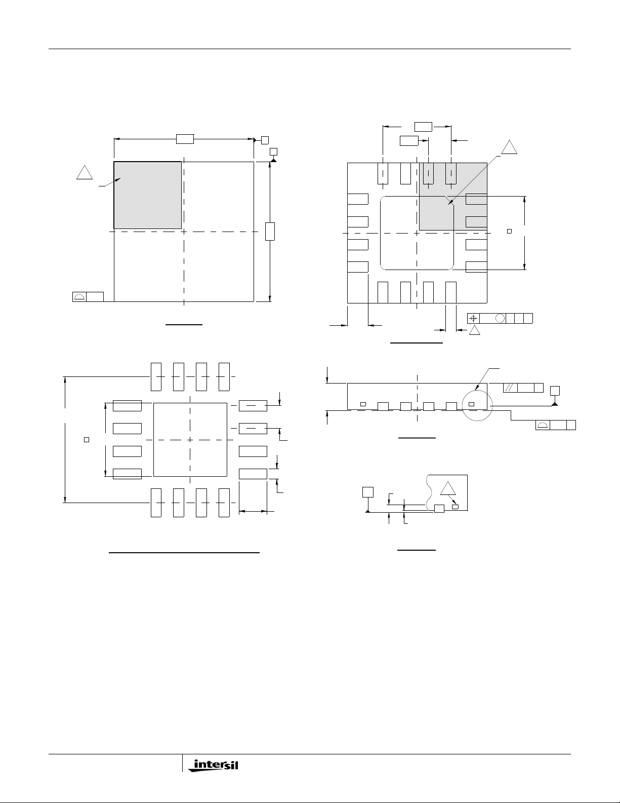
Package Outline Drawing
L16.4x4
16 LEAD QUAD FLAT NO-LEAD PLASTIC PACKAGE
Rev 6, 02/08
4.00
6
PIN 1
INDEX AREA
ISL8013
A
B
4X 1.95
0.65
12X
13
12
16
6
PIN #1 INDEX AREA
1
(4X)
( 3 . 6 TYP )
0.15
( 2 . 10 )
TOP VIEW
4.00
16X 0 . 60
( 16X 0 . 28 )
( 16 X 0 . 8 )
+0.15
-0.10
1.00 MAX
( 12X 0 . 65 )
2 . 10 ± 0 . 15
9
8
BOTTOM VIEW
SIDE VIEW
0 . 2 REF
C
0 . 00 MIN.
0 . 05 MAX.
5
5
0.10 CM
4
0.28 +0.07 / -0.05
4
A B
SEE DETAIL "X"
0.10
BASE PLANE
SEATING PLANE
C
C
0.08 C
TYPICAL RECOMMENDED LAND PATTERN
17
DETAIL "X"
NOTES:
Dimensions are in millimeters.1.
Dimensions in ( ) for Reference Only.
Dimensioning and tolerancing conform to AMSE Y14.5m-1994.
2.
3.
Unless otherwise specified, tolerance : Decimal ± 0.05
Dimension b applies to the metallized terminal and is measured
4.
between 0.15mm and 0.30mm from the terminal tip.
Tiebar shown (if present) is a non-functional feature.
5.
The configuration of the pin #1 identifier is optional, but must be
6.
located within the zone indicated. The pin #1 identifier ma y be
either a mold or mark feature.
November 23, 2009
FN6309.3
 Loading...