

Page 1
High Performance 2A and 3A LDOs
ISL80102, ISL80103
ISL80102, ISL80103
The ISL80102 and ISL80103 are low voltage,
high-current, single output LDOs specified for 2A and 3A
output current, respectively. These parts operate from
input voltages of 2.2V to 6V and are capable of providing
output voltages of 0.8V to 5V on the adjustable V
OUT
versions. Fixed output voltage options available in 0.8V,
1.2V, 1.5V, 1.8V, 2.5V, 3.3V and 5V. Other custom
voltage options availabl e upon request.
For applications that demand in-rush current less than
current limit, an external capacitor on the in-rush set pin
provides adjustment. The ENABLE feature allows the part
to be placed into a low quiescent current shutdown
mode. Sub-micron CMOS process is utilized for this
product family to deliver the best in class analog
performance and overall value.
These CMOS LDOs will consume significantly lower
quiescent current as a function of load over bipolar LDOs,
which translates into higher efficiency and the ability to
consider packages with smaller footprints. Quiescent
current is modestly compromised to enable a leading
class fast load transient response, and hence a lower
total AC regulation band for an LDO in this category .
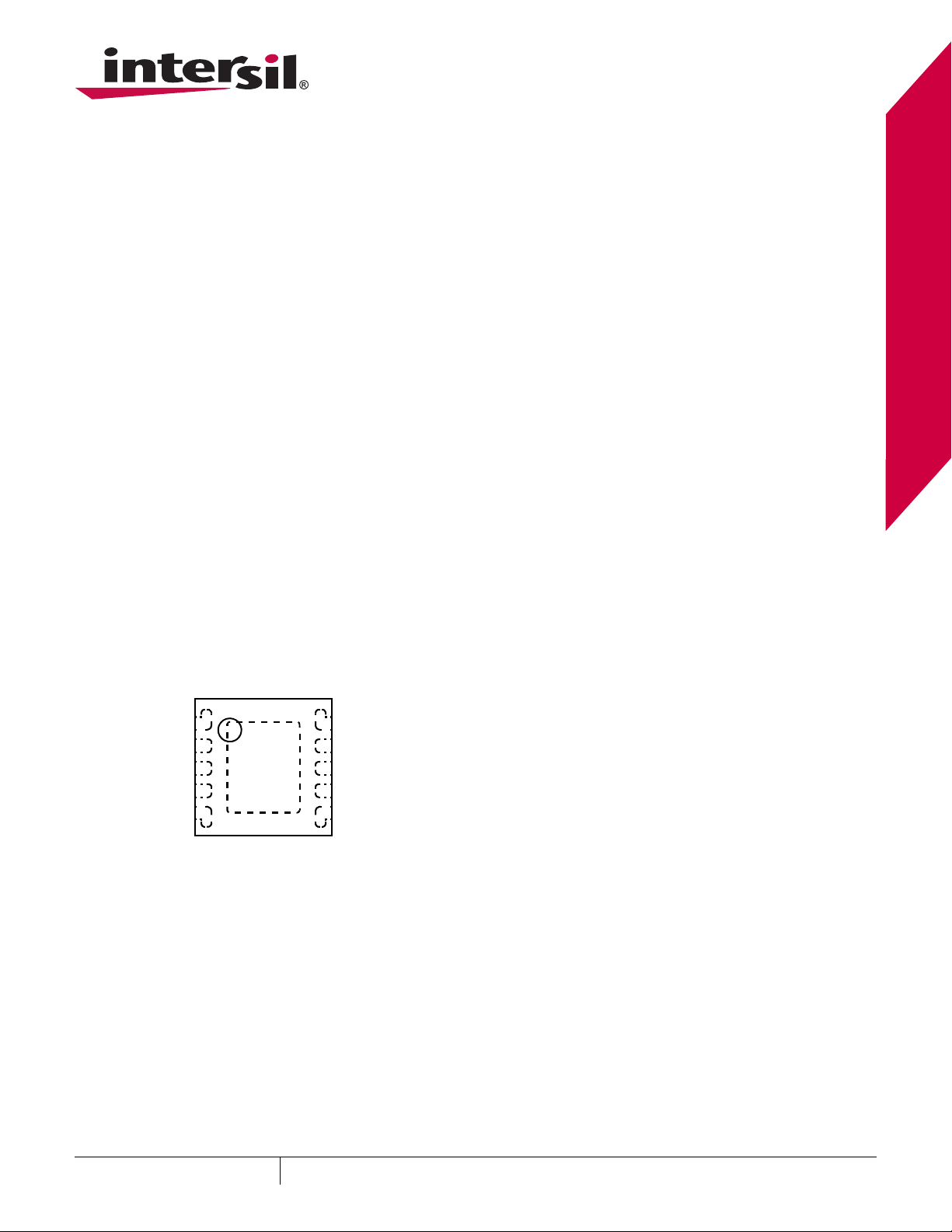
Pin Configuration
ISL80102, ISL80103
(10 LD 3X3 DFN)
TOP VIEW
V
OUT
V
OUT
SENSE/ADJ
PG
GND
1
2
3
4
5
10
9
8
7
6
V
IN
V
IN
DNC
ENABLE
SS
Features
• 0.5% initial V
• Designed for 2.2V to 6V Input Supply
• ±1.8% Guaranteed V
Temperature Range from -40°C to +125°C
• 185mV Dropout @ 3A, 125mV Dropout @ 2A
• Fast Load Transient Response
• Rated Output Current Options of 2A and 3A
• Adjustable In-Rush Current Limiting
• Fixed and Adjustable V
• 65dB Typical PSRR
• Output Noise of 100µV
300kHz
•PG Feature
•900mV Enable Input Threshold
• Short-Circuit Current Protection
• 1A Peak Reverse Current
• Over-Temperature Shutdown
• Any Cap Stable with Minimum 10µF Ceramic
• Available in a 10 Ld DFN Package and soon to follow
TO220-5, TO263-5 and SOT223-5 (1A and 2A
versions)
• Pb-Free (RoHS Compliant)
Accuracy
OUT
Accuracy for Junction
OUT
Options Available
OUT
between 300Hz to
RMS
Applications*(see page 15)
• DSP, FPGA and µP Core Power Supplies
• Noise-Sensitive Instrumentation Systems
• Post Regulation of Switched Mode Power Supplies
• Industrial Systems
•Medical Equipment
• Telecommunications and Networking Equipment
•Servers
• Hard Disk Drives (HD/HDD)
September 30, 2009
FN6660.0
1
CAUTION: These devices are sensitive to electrostatic discharge; follow proper IC Handling Procedures.
1-888-INTERSIL or 1-888-468-3774
| Intersil (and design) is a regi s t ered trademark of Intersil Americas Inc.
All other trademarks mentioned are the property of their respective owners.
Copyright Intersil Americas Inc. 2009. All Rights Reserved
Page 2
ISL80102, ISL80103
Pin Descriptions
PIN NUMBER PIN NAME DESCRIPTION
1, 2 V
OUT
Output voltage pin.
3 SENSE/ADJ Remote voltage sense for internally fixed V
V
.
OUT
4PGV
in regulation signal. Logic low defines when V
OUT
grounded if not used.
5GNDGND pin.
6 SS External cap controls in-rush current.
7ENABLE V
independent chip enable. TTL and CMOS compatible.
IN
8 DNC Do not connect this pin to ground or supply. Leave floating.
9, 10 V
IN
Input supply pin.
EPAD Must be soldered directly to GND plane
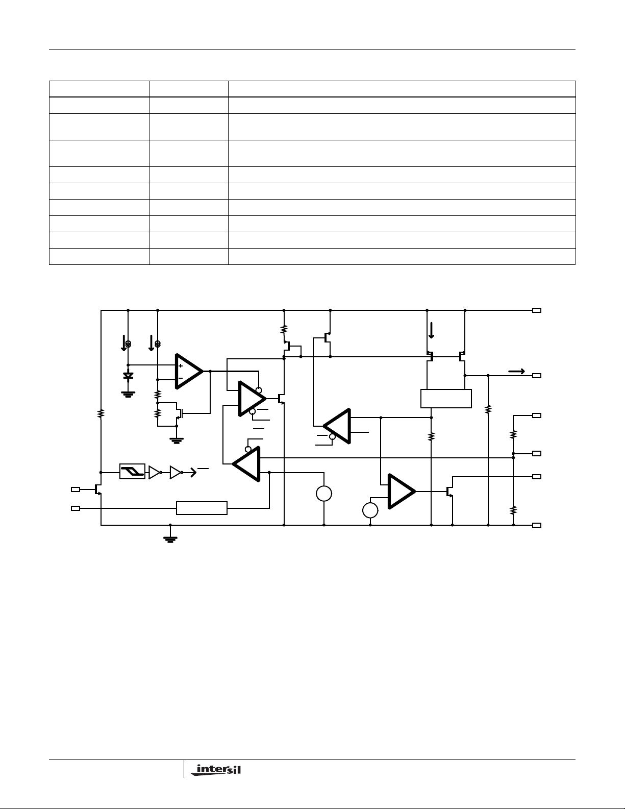
Block Diagram
options. ADJ pin for externally set
OUT
is not in regulation. Must be
OUT
VIN
EN
SS
10µA
R7
M7
10µA
R9
R8
ENEN
V TO I
+
-
IL/10,000
M3
-
+
LEVEL
SHIFT
R4
M1
POWER PMOS
IL
R1
M2
VOUT
SNS
R2
ADJ
PG
R3
GND
R4
M5
+
EN
EN
+
-
500mV
EN
+-+
-
M4
500mV
+
485mV
2
September 30, 2009
FN6660.0
Page 3
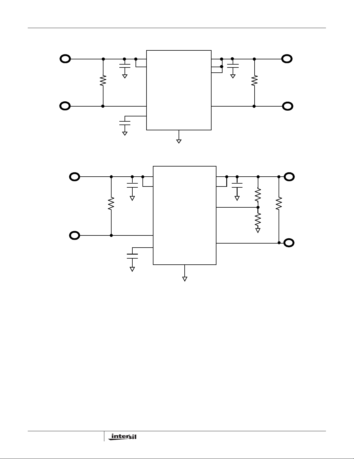
Typical Applications
ISL80102, ISL80103
2.5V ± 10% 1.8V ± 1.8%
10µF 10
10k
(*Note 12)
9
10
7
6
V
IN
V
IN
ENABLE
SS
ISL80102
ISL80103
GN D
5
FIXED
V
V
SENSE/ADJ
OUT
OUT
PG
1
2
3
4
µ
F
100k
FIGURE 1.
V
V
OUT
OUT
1
2
2.6k
100k
1k
10
9
V
IN
IN
ISL80102
ISL80103
SE
NSE/ADJ
V
2.5V ± 10% 1.8V ± 1.8%
10µF 10µF
10k
(*NOTE 12)
7
6
ENABLE
SS
FIGURE 2.
GND
5
JUSTABLE
AD
PG
4
3
September 30, 2009
FN6660.0
Page 4
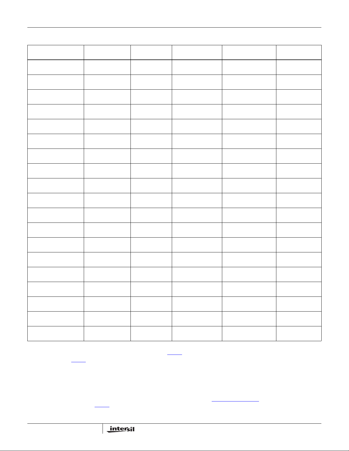
Ordering Information
ISL80102, ISL80103
PART NUMBER
ISL80102IRAJZ
(Notes 1, 3)
ISL80102IR08Z
(Notes 1, 3)
ISL80102IR12Z
(Notes 1, 3)
ISL80102IR15Z
(Notes 1, 3)
ISL80102IR18Z
(Notes 1, 3)
ISL80102IR25Z
(Notes 1, 3)
ISL80102IR33Z
(Notes 1, 3)
ISL80102IR50Z
(Notes 1, 3)
ISL80103IRAJZ
(Notes 1, 3)
ISL80103IR08Z
(Notes 1, 3)
ISL80103IR12Z
(Notes 1, 3)
ISL80103IR15Z
(Note 3)
ISL80103IR15Z-T
(Notes 2, 3)
ISL80103IR18Z
(Notes 1, 3)
ISL80103IR25Z
(Notes 1, 3)
ISL80103IR33Z
(Note 3)
ISL80103IR33Z-T
(Notes 2, 3)
ISL80103IR50Z
(Note 3)
ISL80103IR50Z-T
(Notes 2, 3)
NOTES:
1. Add “-T” or “-TK” suffix for tape and reel. Please refer to TB347
2. Please refer to TB347
3. These Intersil Pb-free plastic pac kaged products employ special Pb-free material sets, molding compounds/die attach
materials, and 100% matte tin plate plus anneal (e3 termination finish, which is RoHS compliant and compatible with both
SnPb and Pb-free soldering operations). Intersil Pb-free products are MSL classified at Pb-free peak reflow temperatures that
meet or exceed the Pb-free requirements of IPC/JEDEC J STD-020 .
4. For other output voltages, contact Intersil Marketing.
5. For Moisture Sensitivity Level (MSL), please see device information page for ISL80102,
MSL please see techbrief TB363
PART
MARKING
DZJA ADJ -40 to +125 10 Ld 3x3 DFN L10.3x3
DZKA 0.8V -40 to +125 10 Ld 3x3 DFN L10.3x3
DZLA 1.2V -40 to +125 10 Ld 3x3 DFN L10.3x3
DZMA 1.5V -40 to +125 10 Ld 3x3 DFN L10.3x3
DZNA 1.8V -40 to +125 10 Ld 3x3 DFN L10.3x3
DZPA 2.5V -40 to +125 10 Ld 3x3 DFN L10.3x3
DZRA 3.3V -40 to +125 10 Ld 3x3 DFN L10.3x3
DZSA 5.0V -40 to +125 10 Ld 3x3 DFN L10.3x3
DZAA ADJ -40 to +125 10 Ld 3x3 DFN L10.3x3
DZBA 0.8V -40 to +125 10 Ld 3x3 DFN L10.3x3
DZCA 1.2V -40 to +125 10 Ld 3x3 DFN L10.3x3
DZDA 1.5V -40 to +125 10 Ld 3x3 DFN L10.3x3
DZDA 1.5V -40 to +125 10 Ld 3x3 DFN
DZEA 1.8V -40 to +125 10 Ld 3x3 DFN L10.3x3
DZFA 2.5V -40 to +125 10 Ld 3x3 DFN L10.3x3
DZGA 3.3V -40 to +125 10 Ld 3x3 DFN L10.3x3
DZGA 3.3V -40 to +125 10 Ld 3x3 DFN
DZHA 5.0V -40 to +125 10 Ld 3x3 DFN L10.3x3
DZHA 5.0V -40 to +125 10 Ld 3x3 DFN
for details on reel specifications.
.
V
OUT
(Note 4)
VOLTAGE
TEMP. RANGE
(°C)
for details on reel specifications.
PACKAGE
(Pb-Free)
Tape and Reel
Tape and Reel
Tape and Reel
ISL80103. For more information on
PKG
DWG. #
L10.3x3
L10.3x3
L10.3x3
4
September 30, 2009
FN6660.0
Page 5
ISL80102, ISL80103
Absolute Maximum Ratings (Note 8) Thermal Information
VIN relative to GND . . . . . . . . . . . . . . . . . . -0.3V to +6.5V
V
relative to GND . . . . . . . . . . . . . . . . . -0.3V to +6.5V
OUT
PG, ENABLE, SENSE/ADJ, SS
Relative to GND. . . . . . . . . . . . . . . . . . . . -0.3V to +6.5V
Recommended Operating Conditions
Junction Temperature Range (TJ) . . . . . . . -40°C to +125°C
VIN relative to GND . . . . . . . . . . . . . . . . . . . . . 2.2V to 6V
V
range . . . . . . . . . . . . . . . . . . . . . . . . . .800mV to 5V
OUT
PG, ENABLE, SENSE/ADJ, SS relative to GND . . . . .0V to 6V
PG sink current . . . . . . . . . . . . . . . . . . . . . . . . . . . . 10mA
CAUTION: Do not operate at or near the maximum ratings listed for extended periods of time. Exposure to such conditions may adversely impact
product reliability and result in failures not covered by warranty.
NOTES:
is measured in free air with the component mounted on a high effective th ermal conductivity test board with “direct attach”
6. θ
JA
features. See Tech Brief TB379.
7. For θ
8. ABS max voltage rating is defined as the voltage applied for a lifetime average duty cycle above 6V of 1%.
, the “case temp” location is the center of the exposed metal pad on the package underside.
JC
Thermal Resistance (Typical) θ
(°C/W) θJC (°C/W)
JA
10 Ld 3x3 DFN Package (Notes 6, 7) 45 4
Maximum Junction Temperature (Plastic Package). . . +150°C
Storage Temperature Range. . . . . . . . . . . - 65°C to +150°C
Pb-Free Reflow Profile . . . . . . . . . . . . . . . . . .see link below
http://www.intersil.com/pbfree/Pb-FreeReflow.asp
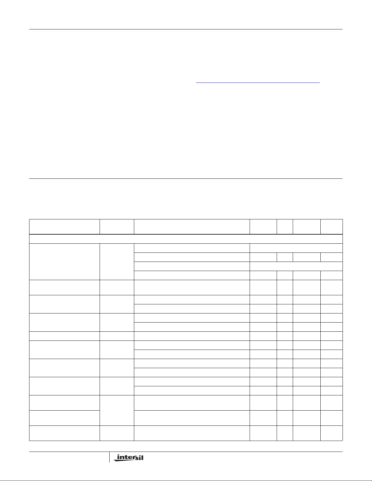
Electrical Specifications Unless otherwise noted, all parameters are established over the following specified
conditions: V
Applications must follow thermal guidelines of the package to determine worst case junction
temperature. Please refer to “Application Section” on page 7 and Tech Brief TB379.
Boldface limits apply over the operating temperature range, -40°C to +125°C. Pulse
load techniques used by ATE to ensure T
PARAMETER SYMBOL TEST CONDITIONS
DC CHARACTERISTICS
DC Output Voltage
Accuracy
Feedback Pin (ADJ option
only)
DC Input Line Regulation ΔV
DC Output Load Regulation ΔV
V
V
OUT
OUT
OUT
FB
T
/ΔVINV
/ΔI
OU
Feedback Input Current V
Ground Pin Current I
Ground Pin Current in
I
SHDN
Q
Shutdown
Dropout Voltage (Note 10) V
Output Short Circuit
DO
ISC V
Current (3A Version)
Output Short Circuit
Current (2A Version)
Thermal Shutdown
Temperature
TSD
= V
IN
V
Options: 0.8V, 1.2V, 1.5V and 1.8V
OUT
2.2V < V
Options: 2.5V, 3.3V and 5.0V
V
OUT
+ 0.4V < V
V
OUT
2.2V < V
+ 0.4V < V
OUT
+ 0.4V < V
V
OUT
0A < I
LOAD
0A < I
LOAD
= 0.5V 0.01 1 µA
ADJ
I
= 0A, 2.2V < V
LOAD
= 3A, 2.2V < V
I
LOAD
ENABLE Pin = 0.2V, V
ENABLE Pin = 0.2V, V
I
= 3A, V
LOAD
= 2A, V
I
LOAD
= 0V, V
OUT
V
= 0V, V
OUT
V
+ 0.4V < V
OUT
+ 0.4V, V
OUT
< 3.6V; 0A < I
IN
IN
< 6V, 0A < I
IN
IN
IN
< 6V; 0A < I
< 3.6V, V
< 6V, V
= 1.8V, C
OUT
= TA defines established limits.
J
< 3A -1.8 0.5 1.8 %
LOAD
LOAD
< 3A 491 500 509 mV
LOAD
= 1.8V 0.1 0.4 %
OUT
= 2.5V 0.1 0.8 %
OUT
IN
= C
= 10µF, TJ = +25°C, IL = 0A
OUT
MIN
(Note 9) TYP
MAX
(Note 9) UNITS
< 3A -1.8 0.5 -1.8 %
< 3A, All voltage options -0.8 %
< 2A, All voltage options -0.6 %
< 6V 7.5 9 mA
IN
< 6V 8.5 12 mA
IN
= 5V 0.4 µA
IN
= 6V 3.3 16 µA
IN
= 2.5V 120 185 mV
OUT
= 2.5V 81 125 mV
OUT
+ 0.4V < V
OUT
+ 0.4V < V
OUT
< 6V 160 °C
IN
< 6V 5.0 A
IN
< 6V 2.8 A
IN
5
September 30, 2009
FN6660.0
Page 6
ISL80102, ISL80103
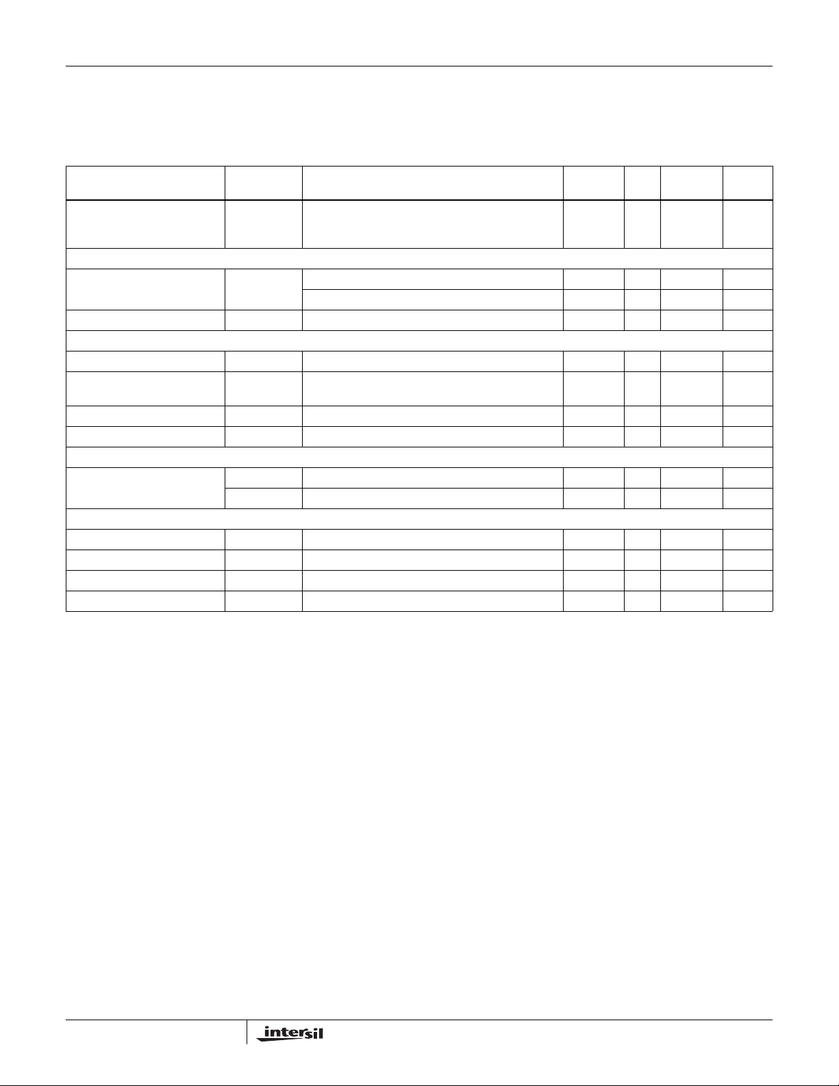
Electrical Specifications Unless otherwise noted, all parameters are established over the following specified
conditions: V
Applications must follow thermal guidelines of the package to determine worst case junction
temperature. Please refer to “Application Section” on page 7 and Tech Brief TB379.
Boldface limits apply over the operating temperature range, -40°C to +125°C. Pulse
load techniques used by ATE to ensure T
PARAMETER SYMBOL TEST CONDITIONS
Thermal Shutdown
TSDn
Hysteresis (Rising
Threshold)
AC CHARACTERISTICS
Input Supply Ripple
PSRR f = 1kHz, I
Rejection
Output Noise Voltage I
ENABLE PIN CHARACTERISTICS
Turn-on Threshold 2.2V < V
Hysteresis (rising
threshold)
Enable Pin Turn-on Delay C
Enable Pin Leakage Current V
SOFT START CHARACTERISTI CS
In-rush Current Limit
Adjust
R
I
CHG
PD
PG PIN CHARACTERISTICS
PG Flag Threshold 75 84 92 %V
V
OUT
V
PG Flag Hysteresis 4%
OUT
PG Flag Low Voltage I
PG Flag Leakage Current V
NOTES:
9. Parameters with MIN and/or MAX limits are 100% tested at +25°C, unles s otherwise specified. T emperature limits est ablished
by characterization and are not production tested.
10. Dropout is defined by the difference in supply V
value.
11. Electromigration specification defined as lifetime average junction temperature of +110°C where max rated DC current =
lifetime average current.
12. Minimum cap on V
and V
IN
required for stability.
OUT
13. Used when large bulk capacitance required on V
= V
IN
V
+ 0.4V < V
OUT
f = 120Hz, I
= 10mA, BW = 300Hz < f < 300kHz 100 µV
LOAD
Must be independent of V
= 10µF, I
OUT
= 6V, EN = 3V 1 µA
IN
+ 0.4V, V
OUT
< 6V 15 °C
IN
= 1A; V
LOAD
= 1A; V
LOAD
< 6V 0.3 0.8 0.95 V
IN
= 1A 150 µs
LOAD
= 1.8V, C
OUT
= TA defines established limits. (Continued)
J
= 2.2V 55 dB
IN
= 2.2V 62
IN
, 2.2V < V
IN
= C
IN
< 6V 135 mV
IN
= 10µF, TJ = +25°C, IL = 0A
OUT
MIN
(Note 9) TYP
MAX
(Note 9) UNITS
323 Ω
-7 -4.5 -2 µA
= 500µA 47 100 mV
SINK
= 6V, PG = 6V 0.05 1 µA
IN
and V
IN
for application.
OUT
when the supply produces a 2% drop in V
OUT
from its nominal
OUT
RMS
OUT
6
September 30, 2009
FN6660.0
Page 7
ISL80102, ISL80103
Application Section
Input Voltage Requirements
Despite other output voltages offered, this family of LDOs
is optimized for a true 2.5V to 1.8V conversion where the
input supply can have a tolerance of as much as ±10%
for conditions noted in the “Electrical Specifications” table
on page 5. Minimum guaranteed input voltage is 2.2V.
However, due to the nature of an LDO, V
must be some
IN
margin higher than the output voltage plus dropout at
the maximum rated current of the application if active
filtering (PSRR) is expected from V
IN
to V
OUT
. The
Dropout spec of this family of LDOs has been generously
specified in order to allow applications to design for a
level of efficiency that can accommodate the smaller
outline package for those applications that cannot
accommodate the profile of the TO220/263.
External Capacitor Requirements
GENERAL GUIDELINE
External capacitors are required for proper operation.
Careful attention must be paid to layout guidelines and
selection of capacitor type and value to ensure optimal
performance.
OUTPUT CAPACITOR
The required minimum output capacitor is 10µF X5R/X7R
to ensure stable operation. Lower cost Y5V and Z5U type
ceramic capacitors are acceptable if the size of the
capacitor is larger to compensate for the significantly
lower tolerance over X5R/X7R types (approximately 2x).
Additional capacitors of any value in Ceramic, POSCAP or
Alum/Tantalum Electrolytic types may be placed in
parallel to improve PSRR at higher frequencies and/or
load transient AC output voltage tolerances. This
minimum capacitor must be connected to V
OUT
and
Ground pins of the LDO with PCB traces no longer than
0.5cm.
INPUT CAPACITOR
The minimum input capacitor required for proper
operation is 10µF having a ceramic dielectric. This
minimum capacitor must be connected to V
OUT
and
Ground pins of the LDO with PCB traces no longer than
0.5cm.
Thermal Fault Protection
In the event the die temperature exceeds typically
+160°C, then the output of the LDO will shut down until
the die temperature can cool down to typically +145°C.
The level of power combined with the thermal impedance
of the package (+50°C/W for DFN) will determine if the
junction temperature exceeds the thermal shutdown
temperature specified in the “Electrical Specifications”
table on page 5 (see thermal packaging guidelines).
Current Limit Protection
The ISL80102/3 family of LDOs incorporates protection
against overcurrent due to any short or overload
condition applied to the output pin. The current limit
circuit performs as a constant current source when the
output current exceeds the current limit threshold noted
in the “Electrical Specifications” table on page 5. If the
short or overload condition is removed from V
OUT
, then
the output returns to normal voltage mode regulation. In
the event of an overload condition on the DFN package
the LDO will begin to cycle on and off due to the die
temperature exceeding thermal fault condition. The
TO220/263 package will tolerate higher levels of power
dissipation on the die which may never thermal cycle if
the heatsink of this larger package can keep the die
temperature below the specified typical thermal
shutdown temperature.
Functional Description
Enable Operation
The Enable turn-on threshold is typically 770mV with a
hysteresis of 135mV. The Enable pin doesn't have an
internal pull-up or pull-down resistor. As a result, this pin
must not be left floating. This pin must be tied to V
is not used. A 1k
Ω to 10kΩ pull-up resistor will be
required for applications that use open collector or open
drain outputs to control the Enable pin. The Enable pin
may be connected directly to V
for applications that are
IN
always on.
Soft-Start Operation
The soft start circuit controls the rate at which the output
voltage comes up to regulation at power-up or coming
out of a chip disable. A constant current charges an
external soft start capacitor. The external capacitor
always gets discharged to 0V at start-up of after coming
out of a chip disable. The discharge rate is the RC time
constant of R
effectively limits the amount of in-rush current below the
programmed current limit during start-up or an enable
sequence to avoid an overcurrent fault condition. This
can be an issue for applications that require large,
external bulk capacitances on V
charging current can be seen for a significant period of
time. High in-rush currents can cause V
minimum which could cause V
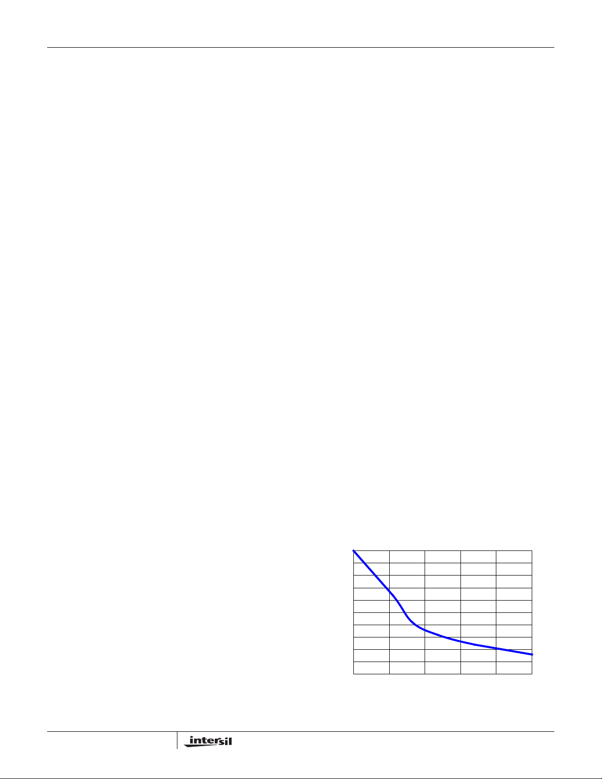
shows the relationship between in-rush current and C
with a C
FIGURE 3. IN-RUSH CURRENT vs SOFT-START
OUT
5.0
4.5
4.0
3.5
3.0
2.5
2.0
1.5
1.0
0.5
IN-RUSH CURRENT LIMIT (A)
0
and CSS. The soft-start function
PD
where high levels of
OUT
to drop below
IN
to shutdown. Figure 3
OUT
of 1000µF.
0 20406080100
CAPACITANCE
Css (nF)
IN
if it
SS
7
September 30, 2009
FN6660.0
Page 8
ISL80102, ISL80103
Power-Good Operation
The PGOOD circuit monitors V
condition when V
is below 84% of the nominal output
OUT
voltage. The PGOOD flag is an open-drain NMOS that can
sink 10mA during a fault condition. The PGOOD pin
requires an external pull up resistor which is typically
connected to the VOUT pin. The PGOOD pin should not
be pulled up to a voltage source greater than V
a fault condition, the PGOOD output is pulled low. The
PGOOD fault can be caused by the current limit fault or
low input voltage. The PGOOD does not function during
thermal shutdown and when the part is disabled.
and signals a fault
OUT
. During
IN
Output Voltage Selection
An external resistor divider is used to scale the output
voltage relative to the internal reference voltage. This
voltage is then fed back to the error amplifier. The output
voltage can be programmed to any level between 0.8V
and 5V. An external resistor divider, R
and R2, is used to
1
set the output voltage as shown in Equation 1. The
recommended value for R
is 500Ω to 1kΩ. R1 is then
2
chosen according to Equation 2:
R
⎛⎞
V
OUT
R
1R2
0.5V
V
OUT
⎛⎞
--------------- -
×=
⎝⎠
0.5V
1+
×=
⎜⎟
R
⎝⎠
2
1–
1
-------
(EQ. 1)
(EQ. 2)
Power Dissipation
The junction temperature must not exceed the range
specified in the Recommended Operating Conditions. The
power dissipation can be calculated by using Equation 3:
VINV
P
D
–()I
OUT
OUTVINIGND
×+×=
(EQ. 3)
The maximum allowed junction temperature, T
J(MAX)
and the maximum expected ambient temperature,
T
A(MAX)
temperature rise (ΔT
ΔT
will determine the maximum allowed junction
) as shown in Equation 4:
J
JTJMAX()TAMAX()
–=
(EQ. 4)
To calculate the maximum ambient operating
temperature, use the junction-to-ambient thermal
resistance (θ
P
DMAX()TJMAX()TA
Substitute P
) for the DFN package with Equation 5:
JA
–()θ
⁄=
JA
for P
D
D(MAX)
and the maximum ambient
(EQ. 5)
operating temperature can be found by solving for TA
using Equation 6:
T
ATJMAXPDMAX()θJA
×–=
(EQ. 6)
Heatsinking The DFN Package
The DFN package uses the copper area on the PCB as a
heat-sink. The EPAD of this package must be soldered to
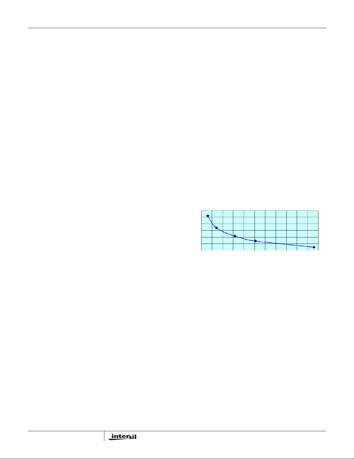
the copper plane (GND plane) for heat sinking. Figure 4
shows a curve for the θ
different copper area sizes.
46
44
42
40
, C/W
JA
38
θ
36
34
24681012141618202224
EPAD-MOUNT COPPER LAND AREA ON PCB, mm
FIGURE 4. 3mmx3mm-10 Pin DFN ON 4-LAYER PCB
WITH THERMAL VIAS θ
COPPER LAND AREA ON PCB
the DFN package for
JA of
JA
2
vs EPAD-MOUNT
8
September 30, 2009
FN6660.0
Page 9
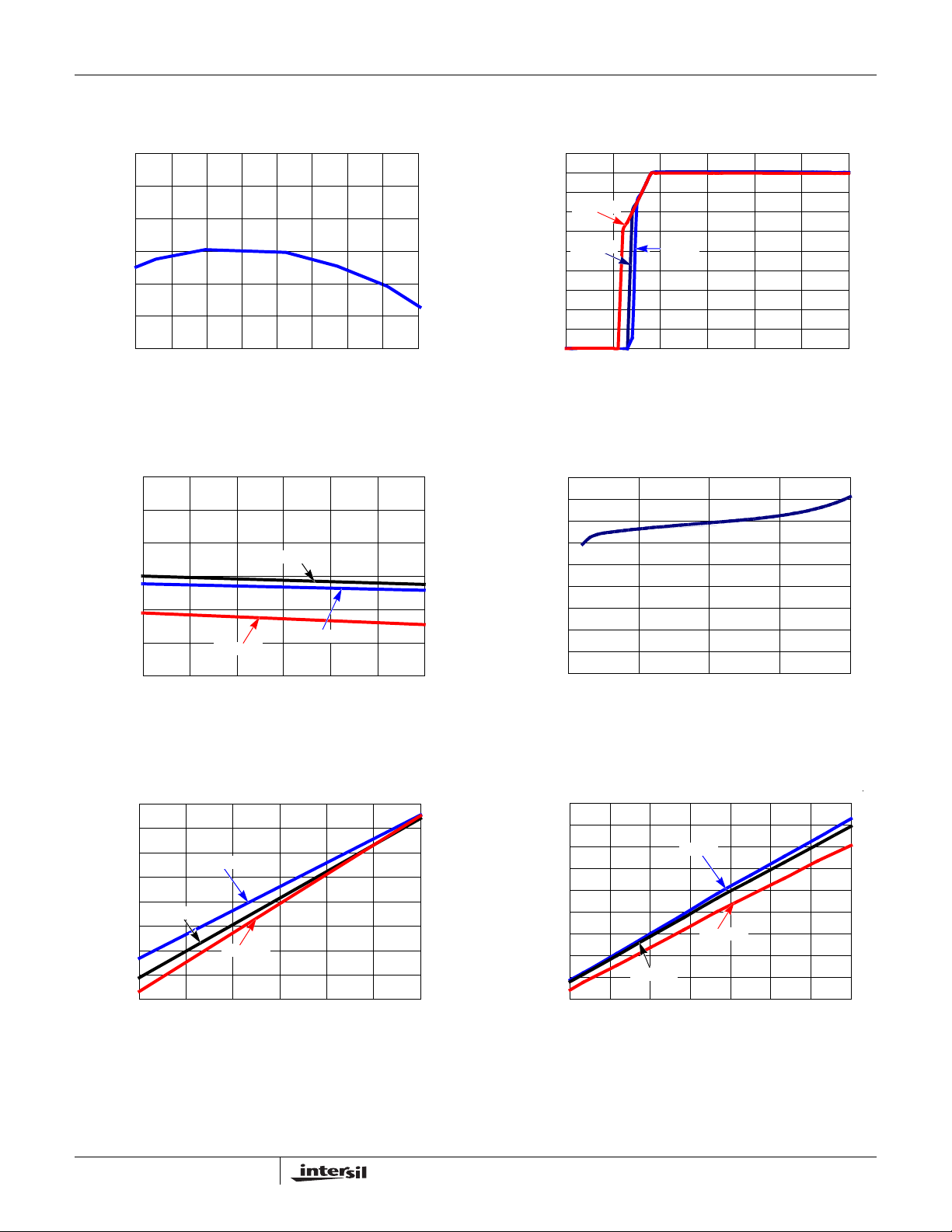
ISL80102, ISL80103
Typical Operating Performance
Unless otherwise noted: VIN = 2.2V, V
1.8
1.2
0.6
(%)
0
OUT
-0.6
ΔV
-1.2
-1.8
-50 -25 0 25 50 75 100 125 150
FIGURE 5. OUTPUT VOLTAGE vs TEMPERATURE
JUNCTION TEMPERATURE (°C)
= 1.8V, CIN = C
OUT
= 10µF, TJ = +25°C, IL = 0A.
OUT
2.0
1.8
1.6
+125°C
1.4
1.2
+25°C
1.0
0.8
0.6
0.4
OUTPUT VOLTAGE (V)
0.2
0
0246
135
-40°C
SUPPLY VOLTAGE (V)
FIGURE 6. OUTPUT VOLTAGE vs SUPPLY VOLTAGE
1.8
1.2
0.6
(%)
0.0
OUT
ΔV
-0.6
-1.2
-1.8
0 0.5 1.0 1.5 2.0 2.5 3.0
+125°C
OUTPUT CURRENT (A)
+25°C
-40°C
FIGURE 7. OUTPUT VOLTAGE vs OUTPUT CURRENT
9.1
8.9
8.7
8.5
8.3
8.1
7.9
GROUND CURRENT (mA)
7.7
7.5
0 0.5 1.0 1.5 2.0 2.5 3.0
-40°C
+25°C
+125°C
OUTPUT CURRENT (A)
FIGURE 9. GROUND CURRENT vs OUTPUT CURRENT
9
8
7
6
5
4
3
2
GROUND CURRENT (mA)
1
0
2
3456
INPUT VOLTAGE (V)
FIGURE 8. GROUND CURRENT vs SUPPLY VOLTAGE
12.0
11.5
11.0
10.5
10.0
9.5
9.0
CURRENT (mA)
8.5
8.0
7.5
0.8 1.4 2.0 2.6 3.2 3.8 4.4 5.0
-40°C
+125°C
+25°C
OUTPUT VOLTAGE (V)
FIGURE 10. GROUND CURRENT vs OUTPUT VOLTAGE
9
September 30, 2009
FN6660.0
Page 10
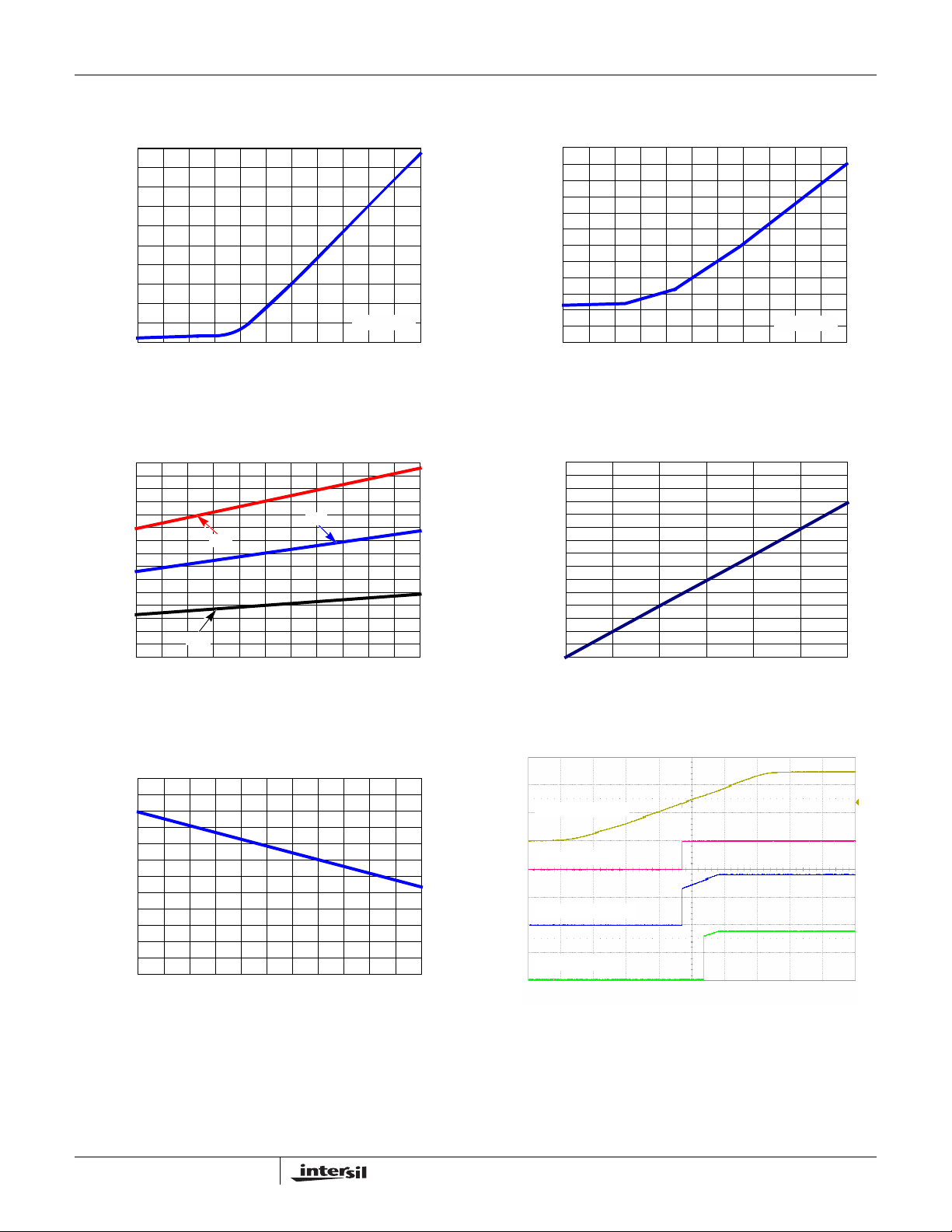
ISL80102, ISL80103
Typical Operating Performance
Unless otherwise noted: VIN = 2.2V, V
5.0
4.5
4.0
3.5
3.0
2.5
2.0
1.5
1.0
GROUND CURRENT (µA)
0.5
0
-40 -25 -10 5 20 35 50 65 80 95 110 125
TEMPERATURE (°C)
FIGURE 11. SHUTDOWN CURRENT vs TEMPERATURE
= 1.8V, CIN = C
OUT
VIN = 5V
= 10µF, TJ = +25°C, IL = 0A. (Continued)
OUT
12
11
10
9
8
7
6
5
4
3
2
GROUND CURRENT (µA)
1
0
-40 -25 -10 5 20 35 50 65 80 95 110 125
TEMPERATURE (°C)
VIN = 6V
FIGURE 12. SHUTDOWN CURRENT vs TEMPERATURE
150
140
130
120
110
100
90
80
70
60
50
40
30
20
DROPOUT VOLTAGE (mV)
10
0
-40 -25 -10 5 20 35 50 65 80 95 110 125
3A
1A
TEMPERATURE (°C)
2A
150
140
130
120
110
100
90
80
70
60
50
40
30
20
DROPOUT VOLTAGE (mV)
10
0
0 0.5 1.0 1.5 2.0 2.5 3.0
OUTPUT CURRENT (A)
FIGURE 13. DROPOUT VOLTAGE vs TEMPERATURE FIGURE 14. DROPOUT VOLTAGE vs OUTPUT CURRENT
0.90
0.85
0.80
0.75
0.70
0.65
0.60
0.55
0.50
VOLTAGE (V)
0.45
0.40
0.35
0.30
-40 -25 -10 5 20 35 50 65 80 95 110 125
JUNCTION TEMPERATURE (°C)
FIGURE 15. ENABLE THRESHOLD VOLTAGE vs
VIN (1V/DIV)
SS (1V/DIV)
V
(1V/DIV)
OUT
PG (1V/DIV)
TIME (10ms/DIV)
FIGURE 16. POWER-UP (V
= 2.2V)
IN
TEMPERATURE
10
September 30, 2009
FN6660.0
Page 11
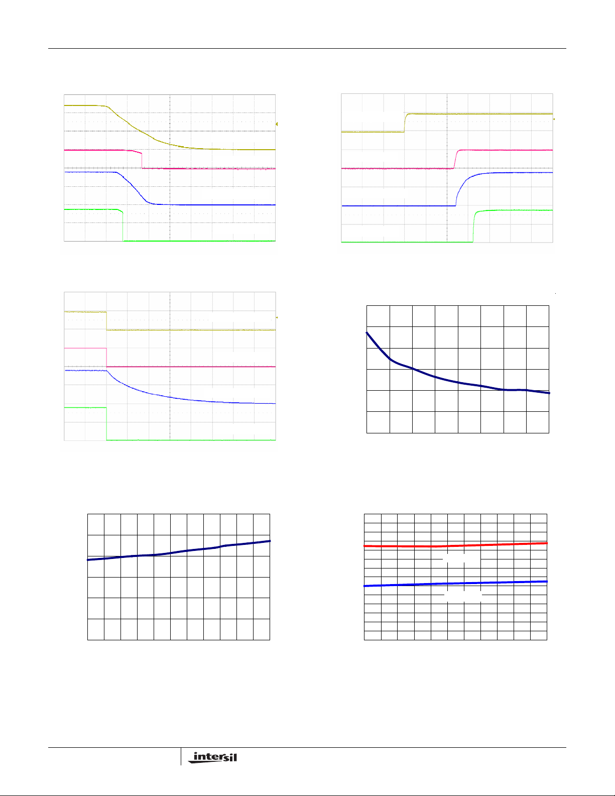
ISL80102, ISL80103
Typical Operating Performance
Unless otherwise noted: VIN = 2.2V, V
= 1.8V, CIN = C
OUT
VIN (1V/DIV)
= 10µF, TJ = +25°C, IL = 0A. (Continued)
OUT
EN (1V/DIV)
SS (1V/DIV)
(1V/DIV)
V
OUT
PG (1V/DIV)
TIME (10ms/DIV)
FIGURE 17. POWER-DOWN (VIN = 2.2V)
EN (1V/DIV)
SS (1V/DIV)
(1V/DIV)
V
OUT
PG (1V/DIV)
TIME (5ms/DIV)
FIGURE 19. ENABLE SHUTDOWN
SS (1V/DIV)
V
(1V/DIV)
OUT
PG (1V/DIV)
TIME (50µs/DIV)
FIGURE 18. ENABLE START-UP
300
250
200
150
100
START-UP TIME (µs)
50
0
2.0 2.5 3.0 3.5 4.0 4.5 5.0 5.5 6.0
INPUT VOLTAGE (V)
FIGURE 20. START-UP TIME vs SUPPLY VOLTAGE
300
250
200
150
100
START-UP TIME (µs)
50
0
-40 -25 -10 5 20 35 50 65 80 95 110 125
JUNCTION TEMPERATURE (°C)
FIGURE 21. START-UP TIME vs TEMPERATURE
11
7.0
6.5
6.0
5.5
5.0
4.5
4.0
3.5
3.0
2.5
2.0
1.5
CURRENT LIMIT (A)
1.0
0.5
0
-40 -25 -10 5 20 35 50 65 80 95 110 125
JUNCTION TEMPERATURE (°C)
ISL80103
ISL80102
FIGURE 22. CURRENT LIMIT vs TEMPERATURE
September 30, 2009
FN6660.0
Page 12
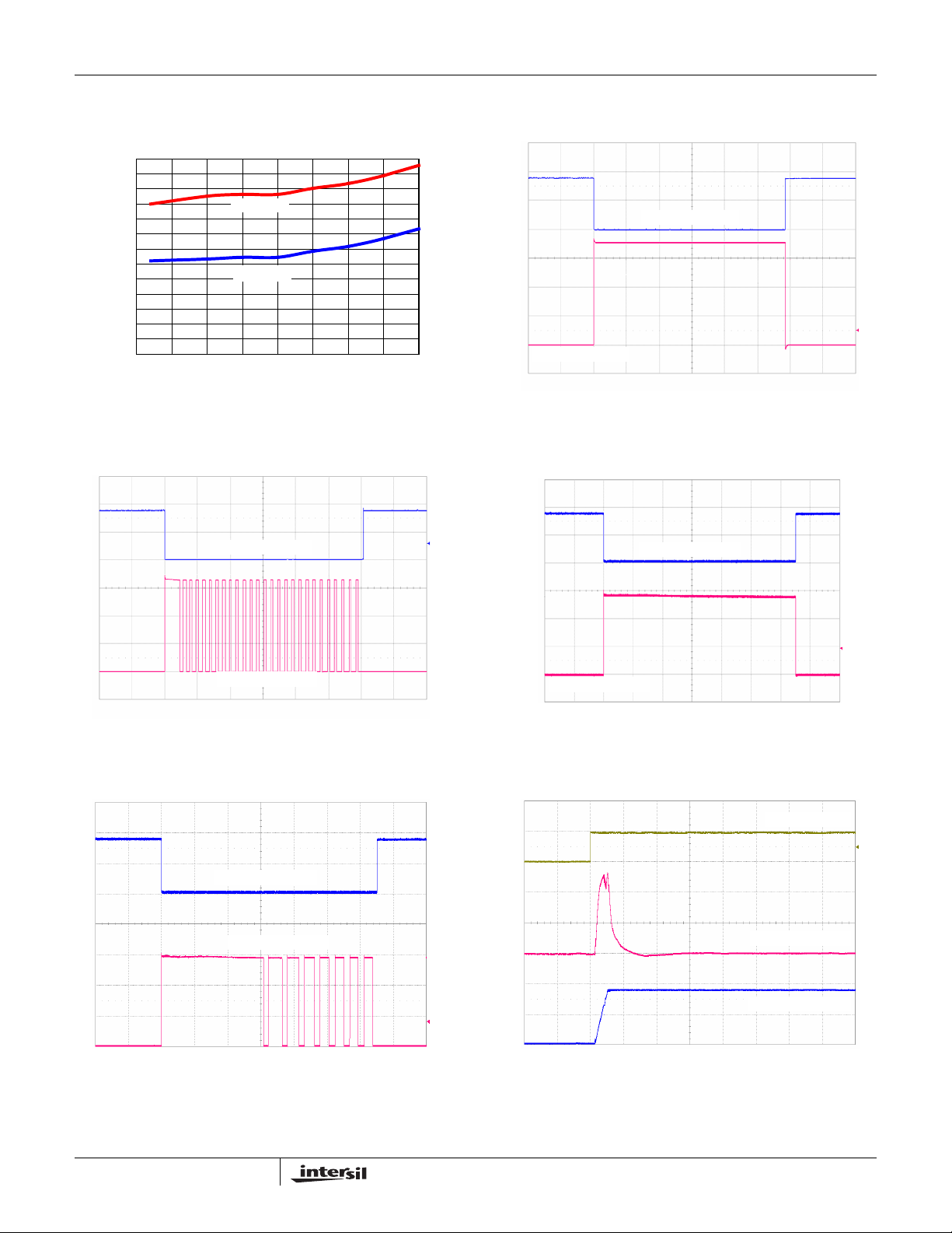
ISL80102, ISL80103
Typical Operating Performance
Unless otherwise noted: VIN = 2.2V, V
6.5
6.0
5.5
5.0
4.5
4.0
3.5
3.0
2.5
2.0
1.5
CURRENT LIMIT (A)
1.0
0.5
0
2.0 2.5 3.0 3.5 4.0 4.5 5.0 5.5 6.0
FIGURE 23. CURRENT LIMIT vs SUPPLY VOLTAGE
ISL80103
ISL80102
INPUT VOLTAGE (V)
= 1.8V, CIN = C
OUT
= 10µF, TJ = +25°C, IL = 0A. (Continued)
OUT
VOUT (1V/DIV)
IOUT (1A/DIV)
TIME (10ms/DIV)
FIGURE 24. CURRENT LIMIT RESPONSE (ISL80102)
(1V/DIV)
V
OUT
I
(1A/DIV)
OUT
TIME (100ms/DIV)
FIGURE 25. THERMAL CYCLING (ISL80102)
V
(1V/DIV)
OUT
I
(2A/DIV)
OUT
V
(1V/DIV)
OUT
I
(2A/DIV)
OUT
TIME (20ms/DIV)
FIGURE 26. CURRENT LIMIT RESPONSE (ISL80103)
EN (1V/DIV)
I
(2A/DIV)
OUT
TIME (50ms/DIV)
FIGURE 27. THERMAL CYCLING (ISL80103)
12
V
OUT
TIME (1ms/DIV)
FIGURE 28. IN-RUSH CURRENT WITH NO
SOFT-START CAPACITOR, C
OUT
September 30, 2009
(1V/DIV)
= 1000µF
FN6660.0
Page 13
ISL80102, ISL80103
Typical Operating Performance
Unless otherwise noted: VIN = 2.2V, V
= 1.8V, CIN = C
OUT
= 10µF, TJ = +25°C, IL = 0A. (Continued)
OUT
EN (1V/DIV)
I
(2A/DIV)
OUT
(1V/DIV)
V
OUT
TIME (1ms/DIV)
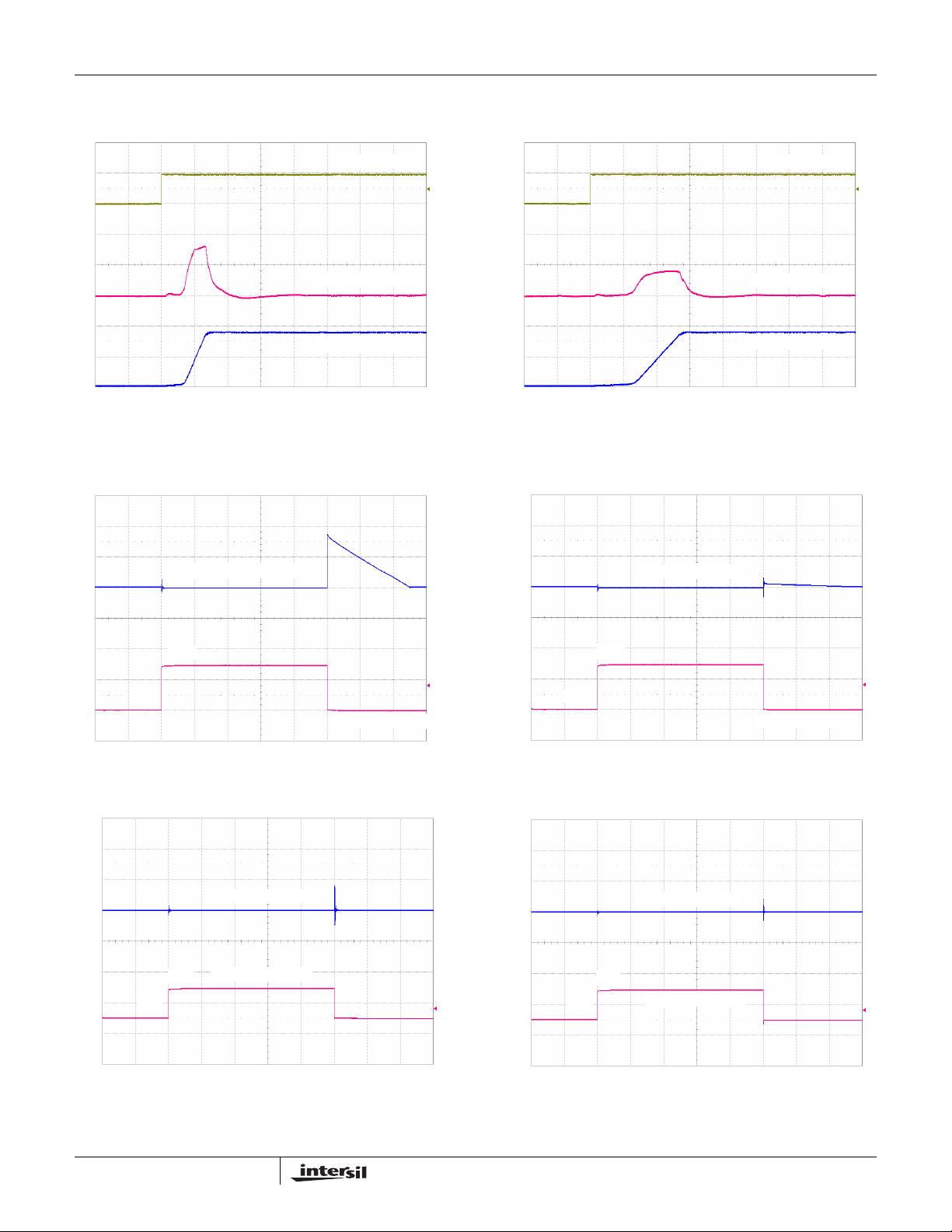
FIGURE 29. IN-RUSH WITH 22nF SOFT-START
CAPACITOR, C
(50mV/DIV)
V
OUT
= 1000µF
OUT
EN (1V/DIV)
I
(2A/DIV)
OUT
V
(1V/DIV)
OUT
TIME (1ms/DIV)
FIGURE 30. IN-RUSH WITH 47nF SOFT-START
CAPACITOR, C
V
OUT
= 1000µF
OUT
(50mV/DIV)
3A
0A
I
OUT
TIME (100µs/DIV)
FIGURE 31. LOAD TRANSIENT 0A TO 3A,
=10µF CERAMIC
C
OUT
(50mV/DIV)
V
OUT
I
3A
1A
(2A/DIV)
OUT
TIME (100µs/DIV)
FIGURE 33. LOAD TRANSIENT 1A TO 3A,
C
=10µF CERAMIC
OUT
(2A/DIV)
3A
0A
I
OUT
TIME (100µs/DIV)
FIGURE 32. LOAD TRANSIENT 0A TO 3A,
C
= 10µF CERAMIC + 100µF OSCON
OUT
V
(50mV/DIV)
OUT
3A
I
(2A/DIV)
1A
OUT
TIME (100µs/DIV)
FIGURE 34. LOAD TRANSIENT 1A TO 3A,
= 10µF CERAMIC + 100µF OSCON
C
OUT
(2A/DIV)
13
September 30, 2009
FN6660.0
Page 14
ISL80102, ISL80103
Typical Operating Performance
Unless otherwise noted: VIN = 2.2V, V
3.2V
2.2V
V
TIME (200µs/DIV)
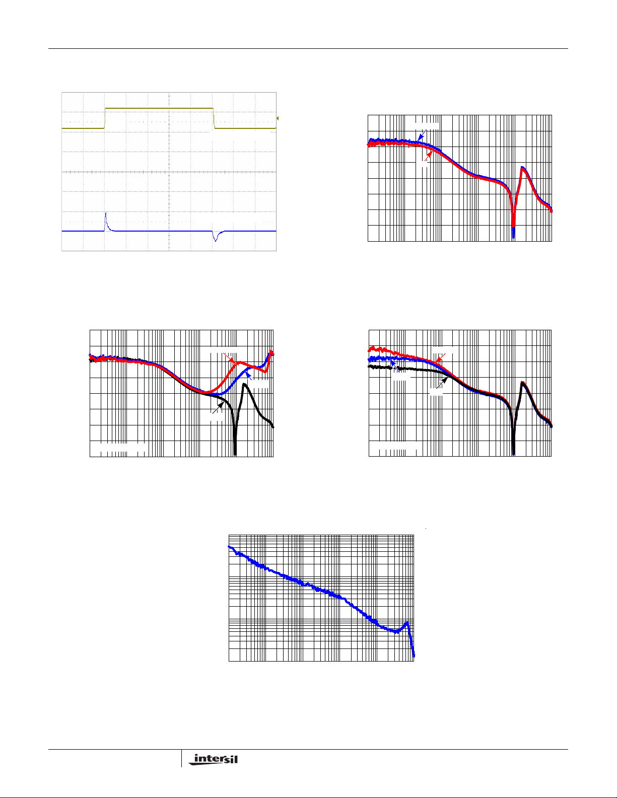
FIGURE 35. LINE TRANSIENT
= 1.8V, CIN = C
OUT
(1V/DIV)
V
IN
(10mV/DIV)
OUT
= 10µF, TJ = +25°C, IL = 0A. (Continued)
OUT
80
70
60
50
40
dB
30
20
10
0
10 100 1k 10k 100k 1M
100mA
1A
FREQUENCY (Hz)
FIGURE 36. PSRR vs LOAD
80
70
60
50
40
dB
30
20
10
IL = 100mA
0
10 100 10k 100k 1M
1k
FREQUENCY (Hz)
FIGURE 37. PSRR vs C
100µF
10µF
OUT
NOISE µV/√Hz
10
1
0.1
47µF
80
70
60
2.2V
IL = 1A
10 100 1k 10k 100k 1M
dB
50
40
30
20
10
0
FIGURE 38. PSRR vs V
2.5V
2V
FREQUENCY (Hz)
IN
0.01
10 100 1k 10k 100k 1M
FREQUENCY (Hz)
FIGURE 39. SPECTRAL NOISE DENSITY vs FREQUENCY
14
September 30, 2009
FN6660.0
Page 15

ISL80102, ISL80103
Revision History
The revision history provided is for informational purposes only and is believed to be accurate, but not warranted. Please go to
web to make sure you have the latest Rev.
DATE REVISION CHANGE
09/30/09 FN6660.0 Initial Release.
Products
Intersil Corporation is a leader in the design and manufacture of high-performance analog semiconductors. The
Company's products address some of the industry's fastest growing markets, such as, flat panel displays, cell phones,
handheld products, and notebooks. Intersil's product families address power management and analog signal
processing functions. Go to www.intersil.com/products
*For a complete listing of Applications, Related Documentation and Related Parts, please see the respective device
information page on intersil.com: ISL80102,
ISL80103
To report errors or suggestions for this datasheet, please go to www.intersil.com/ask ourstaff
FIT s are available from our website at http://rel.intersil.com/reports/search.php
for a complete list of Intersil product families.
For additional products, see www.intersil.com/product_tree
Intersil products are manufactured, assembled and tested utilizing ISO9000 quality systems as noted
in the quality certifications found at www.intersil.com/design/quality
Intersil products are sold by description o nly . In tersil Corporation reserves the right to make changes in circuit design, software and/or specifications
at any time without notice. Accordingly, the reader is cautioned to verify that data sheets are current before placing orders. Information furnished by
Intersil is believed to be accurate and reliable. However, no responsibility is assumed by Intersil or its subsidiaries for its use; nor for any
infringements of patents or other rights of third parties which may result from its use. No license is granted by implication or otherwise under any
patent or patent rights of Intersil or its s ub si di arie s .
For information regarding Intersil Corporation and its products, see www.intersil.com
15
September 30, 2009
FN6660.0
Page 16
Package Outline Drawing
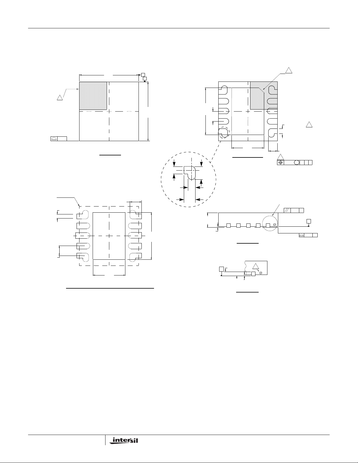
L10.3x3
10 LEAD DUAL FLAT PACKAGE (DFN)
Rev 6, 09/09
3.00
6
PIN 1
INDEX AREA
(4X) 0.10
TOP VIEW
ISL80102, ISL80103
A
B
3.00
0.23
2.00
8x 0.50
0.415
0.200
1.60
BOTTOM VIEW
6
PIN #1 INDEX AREA
1
2
10 x 0.23
10x 0.35
4
(4X) 0.10
4
AB
C
M
PACKAGE
OUTLINE
(8x 0.50)
(10 x 0.55)
(10x 0.23)
1.60
TYPICAL RECOMMENDED LAND PATTERN
0.35
1.00
MAX
0.20
2.00
NOTES:
Dimensions are in millimeters.1.
Dimensions in ( ) for Reference Only.
Dimensioning and tolerancing conform to AMSE Y14.5m-1994.
2.
3.
Unless otherwise specified, tolerance : Decimal ± 0.05
Lead width applies to the metallized terminal and is measured
4.
between 0.18mm and 0.30mm from the terminal tip.
Tiebar shown (if present) is a non-functional feature.
5.
C
SIDE VIEW
0.20 REF
0.05
DETAIL "X"
5
SEE DETAIL "X"
0.10
C
BASE PLANE
SEATING PLANE
C
0.08
C
16
The configuration of the pin #1 identifier is optional, but must be
6.
located within the zone indicated. The pin #1 indentifier may be
either a mold or mark feature.
September 30, 2009
FN6660.0
 Loading...