

Page 1
®
www.BDTIC.com/Intersil
ISL6596
Data Sheet November 2, 2005
Synchronous Rectified MOSFET Driver
The ISL6596 is a high frequency, MOSFET driver optimized
to drive two N-Channel power MOSFETs in a synchronous
buck converter topology. This driver combined with Intersil’s
Multi-Phase Buck PWM controllers forms a complete singlestage core-voltage regulator solution with high efficiency
performance at high switching frequency for advanced
microprocessors.
The IC is biased by a single low voltage supply (5V),
minimizing driver switching losses in high MOSFET gate
capacitance and high switching frequency applications.
Each driver is capable of driving a 3nF load with less than
10ns rise/fall time. Bootstrapping of the upper gate driver is
implemented via an internal low forward drop diode,
reducing implementation cost, complexity, and allowing the
use of higher performance, cost effective N-Channel
MOSFETs. Adaptive shoot-through protection is integrated
to prevent both MOSFETs from conducting simultaneously.
The ISL6596 features 4A typical sink current for the lower
gate driver, enhancing the lower MOSFET gate hold-down
capability during PHASE node rising edge, preventing power
loss caused by the self turn-on of the lower MOSFET due to
the high dV/dt of the switching node.
The ISL6596 also features an input that recognizes a highimpedance state, working together with Intersil multi-phase
3.3V or 5V PWM controllers to prevent negative transients
on the controlled output voltage when operation is
suspended. This feature eliminates the need for the schottky
diode that may be utilized in a power system to protect the
load from negative output voltage damage.
Applications
• Core Voltage Supplies for Intel® and AMD®
Microprocessors
• High Frequency Low Profile High Efficiency DC/DC
Converters
• High Current Low Voltage DC/DC Converters
• Synchronous Rectification for Isolated Power Supplies
Related Literature
• Technical Brief TB389 “PCB Land Pattern Design and
Surface Mount Guidelines for QFN (MLFP) Packages”
• Technical Brief TB363 “Guidelines for Handling and
Processing Moisture Sensitive Surface Mount Devices
(SMDs)”
FN9240.0
Features
• Drives Two N-Channel MOSFETs
• Adaptive Shoot-Through Protection
•0.4Ω On-Resistance and 4A Sink Current Capability
• Supports High Switching Frequency
- Fast Output Rise and Fall Time
- Low Tri-State Hold-Off Time (20ns)
• Support 3.3V and 5V PWM Input
•Low Quiescent Supply Current
• Power-On Reset
• Expandable Bottom Copper Pad for Heat Spreading
• Dual Flat No-Lead (DFN) Package
- Compliant to JEDEC PUB95 MO-220 QFN-Quad Flat
No Leads-Product Outline
- Near Chip-Scale Package Footprint; Improves PCB
Efficiency and Thinner in Profile
• Pb-Free Plus Anneal Available (RoHS Compliant)
Ordering Information
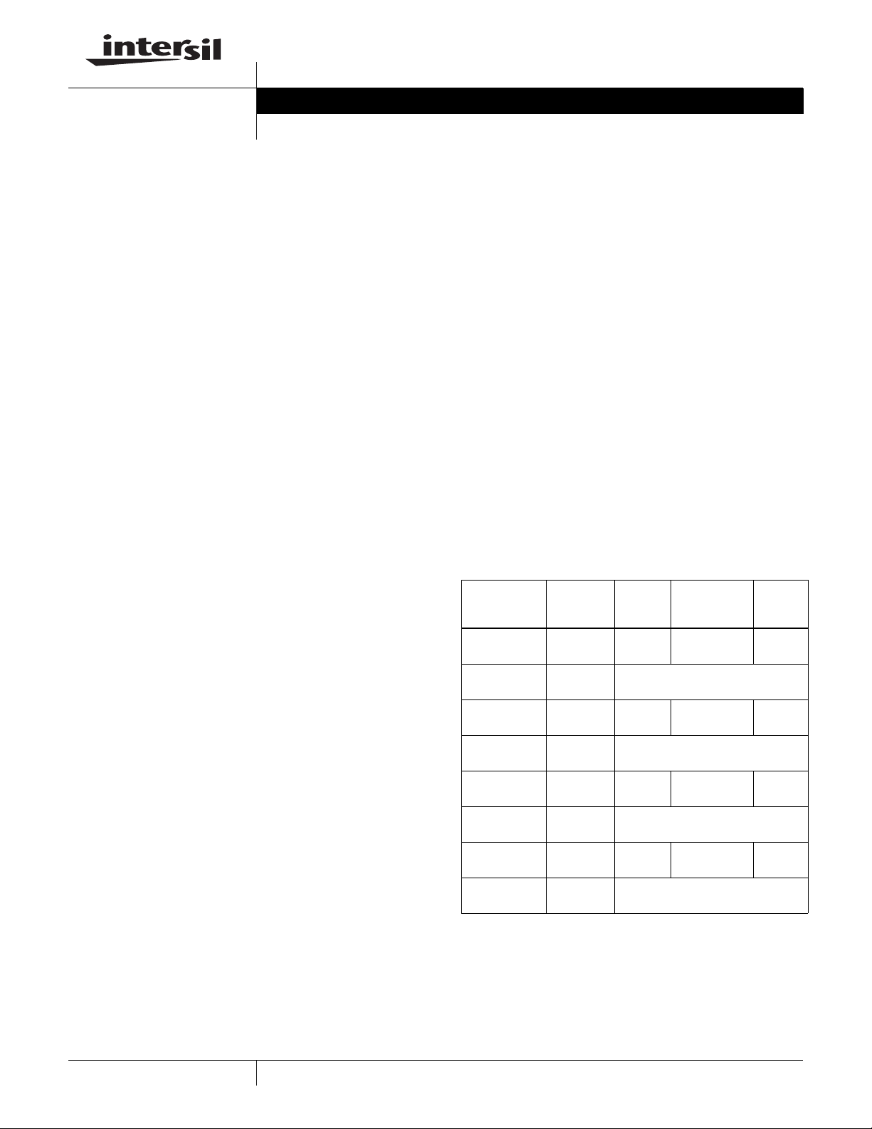
PAR T
NUMBER
ISL6596CBZ
(Note)
ISL6596CBZ-T
(Note)
ISL6596CRZ
(Note)
ISL6596CRZ-T
(Note)
ISL6596IBZ
(Note)
ISL6596IBZ-T
(Note)
ISL6596IRZ
(Note)
ISL6596IRZ-T
(Note)
NOTE: Intersil Pb-free plus anneal products employ special Pb-free
material sets; molding compounds/die attach materials and 100%
matte tin plate termination finish, which are RoHS compliant and
compatible with both SnPb and Pb-free soldering operations. Intersil
Pb-free products are MSL classified at Pb-free peak reflow
temperatures that meet or exceed the Pb-free requirements of
IPC/JEDEC J STD-020.
PART
MARKING
6596CBZ 0 to 70 8 Ld SOIC M8.15
6596CBZ 8 Ld SOIC Tape and Reel
596Z 0 to 70 10 Ld 3x3 DFN L10.3x3
596Z 10 Ld DFN Tape and Reel
96IZ -40 to 85 10 Ld 3x3 DFN L10.3x3
96IZ 10 Ld DFN Tape and Reel
TEMP
RANGE
(°C) PACKAGE
-40 to 85 8 Ld SOIC M8.15
8 Ld SOIC Tape and Reel
PKG.
DWG. #
1
Intel® is a registered trademark of Intel Corporation. AMD® is a registered trademark of Advanced Micro Devices, Inc.
CAUTION: These devices are sensitive to electrostatic discharge; follow proper IC Handling Procedures.
1-888-INTERSIL or 1-888-468-3774 Intersil (and design) is a registered trademark of Intersil Americas Inc.
Copyright © Intersil Americas Inc. 2005. All Rights Reserved
Page 2
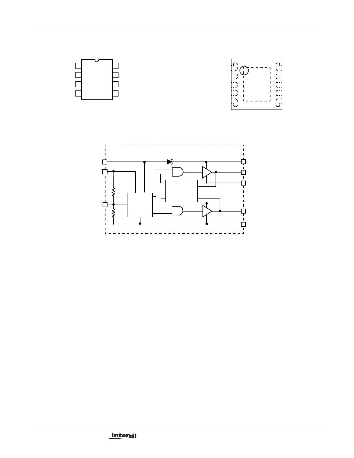
Pinout
www.BDTIC.com/Intersil
ISL6596 (SOIC)
TOP VIEW
ISL6596
ISL6596 (DFN)
TOP VIEW
UGATE
BOOT
PWM
GND
Block Diagram
1
2
3
4
VCC
VCTRL
PWM
8
7
6
5
7k
PHASE
VCTRL
VCC
LGATE
7k
CONTROL
LOGIC
ISL6596
SHOOT-
THROUGH
PROTECTION
UGATE
VCC
BOOT
N/C
PWM
GND
1
2
3
4
5
BOOT
UGATE
PHASE
LGATE
GND
10
9
8
7
6
PHASE
VCTRL
N/C
VCC
LGATE
VCTRL = CONTROLLER VCC
2
FN9240.0
November 2, 2005
Page 3
ISL6596
www.BDTIC.com/Intersil
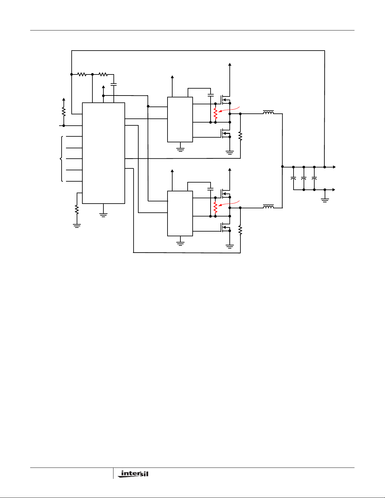
Typical Application - Multi-Phase Converter Using ISL6596 Gate Drivers
V
IN
+5V
+3.3V
PGOOD
VID
(OPTIONAL)
+3.3V
FB
VCC
VSEN
PWM
CONTROLLER
(ISL69XX)
FS/EN
GND
R
ISL6596
ISL6596
BOOT
UGATE
PHASE
LGATE
V
BOOT
UGATE
PHASE
LGATE
COMP
PWM1
PWM2
ISEN1
ISEN2
IS REQUIRED FOR SPECIAL POWER SEQUENCING APPLICATIONS
UGPH
(SEE APPLICATION INFORMATION SECTION ON PAGE 8)
VCC
VCTRL
PWM
+5V
VCC
VCTRL
PWM
IN
R
R
UGPH
UGPH
+V
CORE
3
FN9240.0
November 2, 2005
Page 4
ISL6596
www.BDTIC.com/Intersil
Absolute Maximum Ratings Thermal Information
Supply Voltage (VCC, VCTRL) . . . . . . . . . . . . . . . . . . . -0.3V to 7V
Input Voltage (V
BOOT Voltage (V
BOOT To PHASE Voltage (V
. . . . . . . . . . . . . . . . . . . . . . . . . . . . . . . . . . . . -0.3V to 9V (<10ns)
, V
EN
PWM
BOOT-GND
) . . . . . . . . . . . . . . . -0.3V to VCC + 0.3V
). . . -0.3V to 25V (DC) or 36V (<200ns)
BOOT-PHASE
) . . . . . . -0.3V to 7V (DC)
PHASE Voltage . . . . . . . . . . . . . . . . . . . . . GND - 0.3V to 15V (DC)
. . . . . . . . . GND -8V (<20ns Pulse Width, 10µJ) to 30V (<100ns)
UGATE Voltage . . . . . . . . . . . . . . . . V
. . . . . . . . . . . V
LGATE Voltage . . . . . . . . . . . . . . . GND - 0.3V (DC) to VCC + 0.3V
- 5V (<20ns Pulse Width, 10µJ) to V
PHASE
- 0.3V (DC) to V
PHASE
BOOT
BOOT
. . . . . . . . . . GND - 2.5V (<20ns Pulse Width, 5µJ) to VCC + 0.3V
Ambient Temperature Range . . . . . . . . . . . . . . . . . . . -40°C to 125°C
HBM ESD Rating . . . . . . . . . . . . . . . . . . . . . . . . . . . . . . . . . . . . . 2kV
CAUTION: Stresses above those listed in “Absolute Maximum Ratings” may cause permanent damage to the device. This is a stress only rating and operation of the
device at these or any other conditions above those indicated in the operational sections of this specification is not implied.
Thermal Resistance (Notes 1, 2, & 3) θ
SOIC Package (Note 1) . . . . . . . . . . . . 110 N/A
DFN Package (Notes 2 & 3). . . . . . . . . 48 7
Maximum Junction Temperature . . . . . . . . . . . . . . . . . . . . . . . 150°C
Maximum Storage Temperature Range. . . . . . . . . . . -65°C to 150°C
Maximum Lead Temperature (Soldering 10s) . . . . . . . . . . . . . 300°C
(SOIC - Lead Tips Only)
Recommended Operating Conditions
Ambient Temperature Range. . . . . . . . . . . . . . . . . . . -40°C to 100°C
Maximum Operating Junction Temperature. . . . . . . . . . . . . . 125°C
Supply Voltage, VCC . . . . . . . . . . . . . . . . . . . . . . . . . . . . . 5V ±10%
NOTES:
1. θ
is measured with the component mounted on a high effective thermal conductivity test board in free air. See Tech Brief TB379 for details.
JA
is measured in free air with the component mounted on a high effective thermal conductivity test board with “direct attach” features.
2. θ
JA
, "case temperature" location is at the center of the package underside exposed pad. See Tech Brief TB379 for details.
3. θ
JC
Electrical Specifications These specifications apply for Recommended Operating Conditions, unless otherwise noted.
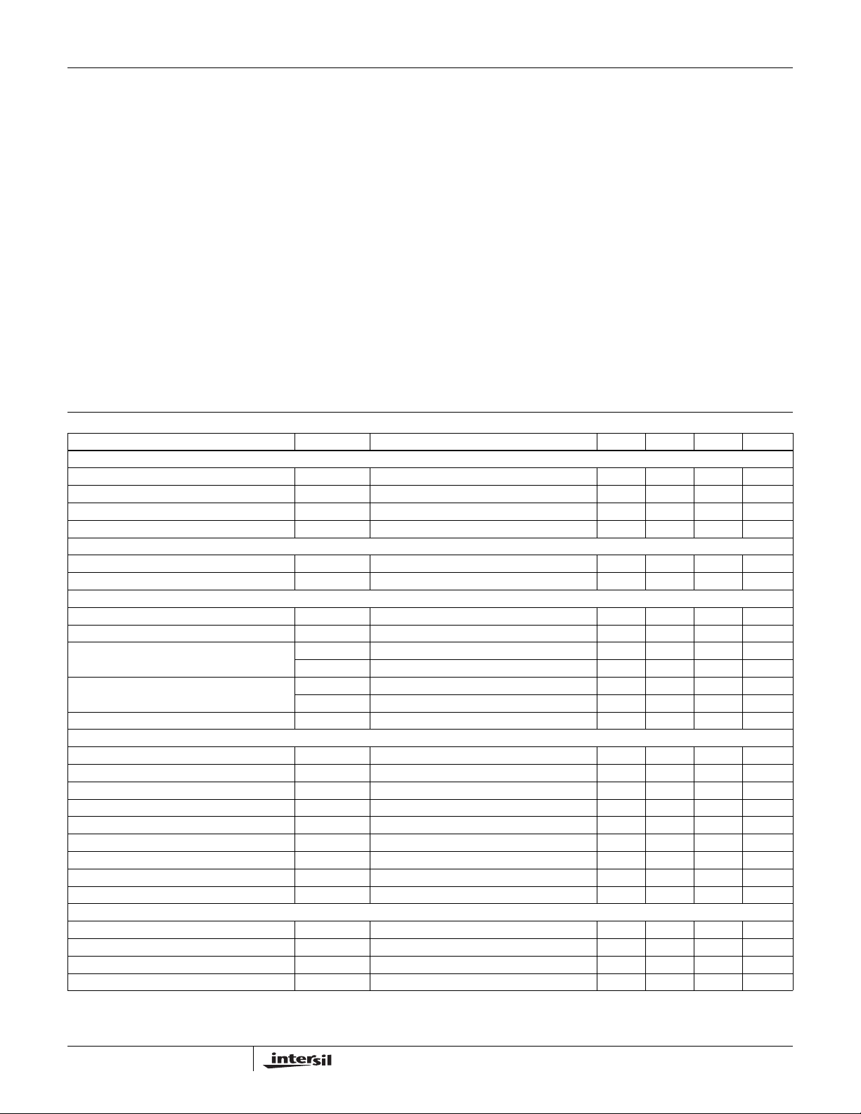
PARAMETER SYMBOL TEST CONDITIONS MIN TYP MAX UNITS
VCC SUPPLY CURRENT
Bias Supply Current I
VCC
POR Rising -3.44.2
POR Falling 2.2 3.0 -
Hysteresis - 400 - mV
VCTRL INPUT
Rising Threshold - 2.75 2.90 V
Falling Threshold 2.4 2.65 - V
PWM INPUT
Sinking Impedance R
Source Impedance R
PWM_SNK
PWM_SRC
Tri-State LowerThreshold V
Tri-State Upper Threshold V
Tri-State Shutdown Holdoff Time t
TSSHDtPDLU
SWITCHING TIME (See Figure 1 on Page 5)
UGATE Rise Time (Note 4) t
LGATE Rise Time (Note 4) t
UGATE Fall Time (Note 4) t
LGATE Fall Time (Note 4) t
UGATE Turn-Off Propagation Delay t
LGATE Turn-Off Propagation Delay t
UGATE Turn-On Propagation Delay t
LGATE Turn-On Propagation Delay t
Tri-state to UG/LG Rising Propagation Delay t
RU
RL
FU
FL
PDLU
PDLL
PDHU
PDHL
PTS
OUTPUT (Note 4)
Upper Drive Source Resistance R
Upper Drive Sink Resistance R
Lower Drive Source Resistance R
Lower Drive Sink Resistance R
UG_SRC
UG_SNK
LG_SRC
LG_SNK
NOTE:
4. Guaranteed by Characterization. Not 100% tested in production.
PWM pin floating, V
= 5V - 190 - µA
VCC
-3.5- kΩ
-3.5- kΩ
= 3.3V (-110mV Hysteresis) - 1.1 - V
VCTRL
V
= 5V (-250mV Hysteresis) - 1.5 - V
VCTRL
= 3.3V (+110mV Hysteresis) - 1.9 - V
VCTRL
= 5V (+250mV Hysteresis) - 3.25 - V
V
VCTRL
or t
+ Gate Falling Time - 20 - ns
PDLL
V
= 5V, 3nF Load - 8.0 - ns
VCC
V
= 5V, 3nF Load - 8.0 - ns
VCC
V
= 5V, 3nF Load - 8.0 - ns
VCC
V
= 5V, 3nF Load - 4.0 - ns
VCC
V
= 5V, Outputs Unloaded - 20 - ns
VCC
V
= 5V, Outputs Unloaded - 15 - ns
VCC
V
= 5V, Outputs Unloaded - 19 - ns
VCC
V
= 5V, Outputs Unloaded - 18 - ns
VCC
V
= 5V, Outputs Unloaded - 30 - ns
VCC
250mA Source Current - 1.0 2.5 Ω
250mA Sink Current - 1.0 2.5 Ω
250mA Source Current - 1.0 2.5 Ω
250mA Sink Current - 0.4 1.0 Ω
(°C/W) θ
JA
JC
(°C/W)
4
FN9240.0
November 2, 2005
Page 5
ISL6596
www.BDTIC.com/Intersil
Functional Pin Description
Note: Pin numbers refer to the SOIC package. Check
diagram for corresponding DFN pinout.
UGATE (Pin 1)
Upper gate drive output. Connect to gate of high-side
N-Channel power MOSFET. A gate resistor is never
recommended on this pin, as it interferes with the operation
shoot-through protection circuitry.
BOOT (Pin 2)
Floating bootstrap supply pin for the upper gate drive.
Connect a bootstrap capacitor between this pin and the
PHASE pin. The bootstrap capacitor provides the charge
used to turn on the upper MOSFET. See the Bootstrap
Considerations section for guidance in choosing the
appropriate capacitor value.
PWM (Pin 3)
The PWM signal is the control input for the driver. The PWM
signal can enter three distinct states during operation, see the
Tri-state PWM Input section for further details. Connect this pin
to the PWM output of the controller.
GND (Pin 4)
Ground pin. All signals are referenced to this node.
LGATE (Pin 5)
Lower gate drive output. Connect to gate of the low side
N-Channel power MOSFET. A gate resistor is never
recommended on this pin, as it interferes with the operation
shoot-through protection circuitry.
VCC (Pin 6)
Connect this pin to a +5V bias supply. Locally bypass with a
high quality ceramic capacitor to ground.
VCTRL (Pin 7)
This pin sets the PWM logic threshold. Connect this pin to
3.3V source for 3.3V PWM input and pull it to 5V source for
5V PWM input.
PHASE (Pin 8)
Connect this pin to the source of the upper MOSFET. This
pin provides the return path for the upper gate driver current.
Thermal Pad (in DFN only)
The metal pad underneath the center of the IC is a thermal
substrate. The PCB “thermal land” design for this exposed
die pad should include vias that drop down and connect to
one or more buried copper plane(s). This combination of
vias for vertical heat escape and buried planes for heat
spreading allows the DFN to achieve its full thermal
potential. This pad should be either grounded or floating,
and it should not be connected to other nodes. Refer to
TB389 for design guidelines.
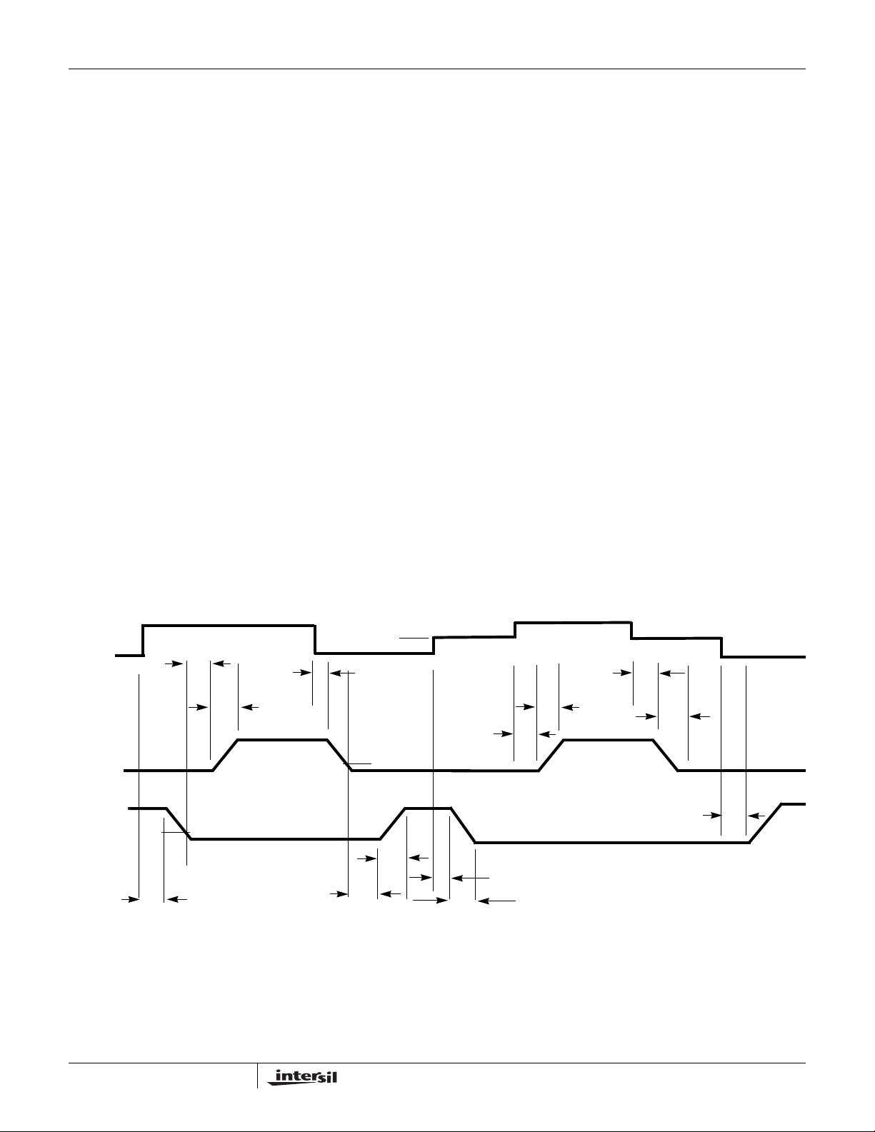
Timing Diagram
PWM
UGATE
LGATE
t
PDLL
t
PDHU
1V
50% of VCC
t
PDLU
t
RU
t
PTS
1V
t
RL
t
t
PDHL
FIGURE 1. TIMING DIAGRAM
t
TSSHD
FL
t
TSSHD
t
RU
t
FU
t
PTS
5
FN9240.0
November 2, 2005
Page 6
ISL6596
www.BDTIC.com/Intersil
Operation and Adaptive Shoot-Through Protection
Designed for high speed switching, the ISL6596 MOSFET
driver controls both high-side and low-side N-Channel FETs
from one externally provided PWM signal.
A rising transition on PWM initiates the turn-off of the lower
MOSFET (see Timing Diagram). After a short propagation
delay [t
[t
] are provided in the Electrical Specifications. Adaptive
FL
shoot-through circuitry monitors the LGATE voltage and turns
on the upper gate following a short delay time [t
the LGATE voltage drops below ~1V. The upper gate drive
then begins to rise [t
A falling transition on PWM indicates the turn-off of the upper
MOSFET and the turn-on of the lower MOSFET. A short
propagation delay [t
begins to fall [t
monitors the UGATE-PHASE voltage and turns on the lower
MOSFET a short delay time, t
gate voltage drops below 1V. The lower gate then rises [t
turning on the lower MOSFET. These methods prevent both the
lower and upper MOSFETs from conducting simultaneously
(shoot-through), while adapting the dead time to the gate
charge characteristics of the MOSFETs being used.
This driver is optimized for voltage regulators with large step
down ratio. The lower MOSFET is usually sized larger
compared to the upper MOSFET because the lower
MOSFET conducts for a longer time during a switching
period. The lower gate driver is therefore sized much larger
to meet this application requirement. The 0.4Ω on-resistance
and 4A sink current capability enable the lower gate driver to
absorb the current injected into the lower gate through the
drain-to-gate capacitor of the lower MOSFET and help
prevent shoot through caused by the self turn-on of the lower
MOSFET due to high dV/dt of the switching node.
], the lower gate begins to fall. Typical fall times
PDLL
PDHU
] and the upper MOSFET turns on.
RU
] is encountered before the upper gate
PDLU
]. The adaptive shoot-through circuitry
FU
, after the upper MOSFET’s
PDHL
] after
RL
],
not exceed either output’s turn-off propagation delay plus the
MOSFET gate discharge time to ~1V. Abnormally long PWM
signal transition times through the shutdown window will simply
introduce additional dead time between turn off and turn on of
the synchronous bridge’s MOSFETs. For optimal performance,
no more than 50pF parasitic capacitive load should be present
on the PWM line of ISL6596 (assuming an Intersil PWM
controller is used).
Bootstrap Considerations
This driver features an internal bootstrap diode. Simply
adding an external capacitor across the BOOT and PHASE
pins completes the bootstrap circuit.
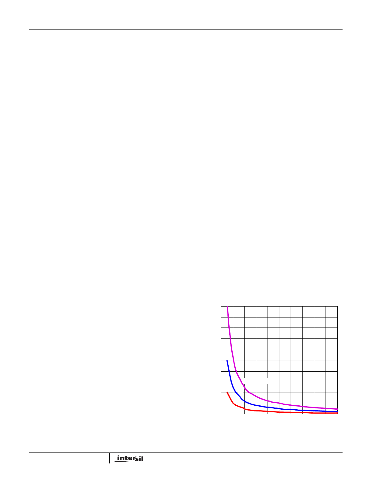
The following equation helps select a proper bootstrap
capacitor size:
Q
GATE
C
BOOT_CAP
Q
GATE
where Q
at V
GS1
control MOSFETs. The ∆V
allowable droop in the rail of the upper gate drive.
As an example, suppose two IRLR7821 FETs are chosen as
the upper MOSFETs. The gate charge, Q
sheet is 10nC at 4.5V (V
Q
GATE
assume a 200mV droop in drive voltage over the PWM
cycle. We find that a bootstrap capacitance of at least
0.110µF is required. The next larger standard value
capacitance is 0.22µF. A good quality ceramic capacitor is
recommended.
--------------------------------------
≥
∆V
BOOT_CAP
QG1VCC•
-------------------------------
V
is the amount of gate charge per upper MOSFET
G1
GS1
•=
N
Q1
gate-source voltage and NQ1 is the number of
BOOT_CAP
) gate-source voltage. Then the
GS
term is defined as the
, from the data
G
is calculated to be 22nC at VCC level. We will
(EQ. 1)
PWM Input and Threshold Control
2.0
A unique feature of the ISL6596 is the programmable PWM
(µF)
BOOT_CAP
C
1.8
1.6
1.4
1.2
1.0
0.8
0.6
0.4
0.2
0.0
20nC
logic threshold set by the control pin (VCTRL) voltage. The
VCTRL pin should connect to the VCC of the controller, thus
the PWM logic threshold follows with the voltage level of the
controller. For 5V applications, this pin can tie to the driver
VCC and simplify the routing.
The ISL6596 also features the adaptable tri-state PWM input.
Once the PWM signal enters the shutdown window, either
MOSFET previously conducting is turned off. If the PWM signal
remains within the shutdown window for longer than the gate
turn-off propagation delay of the previously conducting
MOSFET, the output drivers are disabled and both MOSFET
gates are pulled and held low. The shutdown state is removed
when the PWM signal moves outside the shutdown window.
The PWM rising and falling thresholds outlined in the Electrical
Specifications determine when the lower and upper gates are
enabled. During normal operation in a typical application, the
FIGURE 2. BOOTSTRAP CAPACITANCE vs BOOT RIPPLE
PWM rise and fall times through the shutdown window should
6
Q
GATE
5
0
n
C
VOLTAGE
= 100nC
0.30.0 0.1 0.2 0.4 0.5 0.6 0.90.7 0.8 1.0
∆V
BOOT_CAP
(V)
FN9240.0
November 2, 2005
Page 7
ISL6596
www.BDTIC.com/Intersil
Power Dissipation
Package power dissipation is mainly a function of the
switching frequency (F
external gate resistance, and the selected MOSFET’s
internal gate resistance and total gate charge. Calculating
the power dissipation in the driver for a desired application is
critical to ensure safe operation. Exceeding the maximum
allowable power dissipation level will push the IC beyond the
maximum recommended operating junction temperature of
125°C. The maximum allowable IC power dissipation for the
SO8 package is approximately 800mW at room temperature,
while the power dissipation capacity in the DFN package,
with an exposed heat escape pad, is much higher. See
Layout Considerations paragraph for thermal transfer
improvement suggestions. When designing the driver into an
application, it is recommended that the following calculation
is used to ensure safe operation at the desired frequency for
the selected MOSFETs. The total gate drive power losses
due to the gate charge of MOSFETs and the driver’s internal
circuitry and their corresponding average driver current can
be estimated with Equations 2 and 3, respectively:
P
Qg_TOTPQg_Q1PQg_Q2IQ
QG1VCC
•
P
Qg_Q1
P
Qg_Q2
I
VCC
----------------------------------
V
GS1
QG2VCC
•
----------------------------------
V
GS2
QG1NQ1•
----------------------------- -
V
GS1
), the output drive impedance, the
SW
VCC•++=
2
• NQ1•=
F
SW
2
• NQ2•=
F
SW
•
Q
G2NQ2
----------------------------- -+
V
GS2
VCC F•
+•=
SWIQ
(EQ. 2)
(EQ. 3)
The total gate drive power losses are dissipated among the
resistive components along the transition path. The drive
resistance dissipates a portion of the total gate drive power
losses, the rest will be dissipated by the external gate
resistors (R
and RG2, should be a short to avoid
G1
interfering with the operation shoot-through protection
circuitry) and the internal gate resistors (R
GI1
and R
GI2
) of
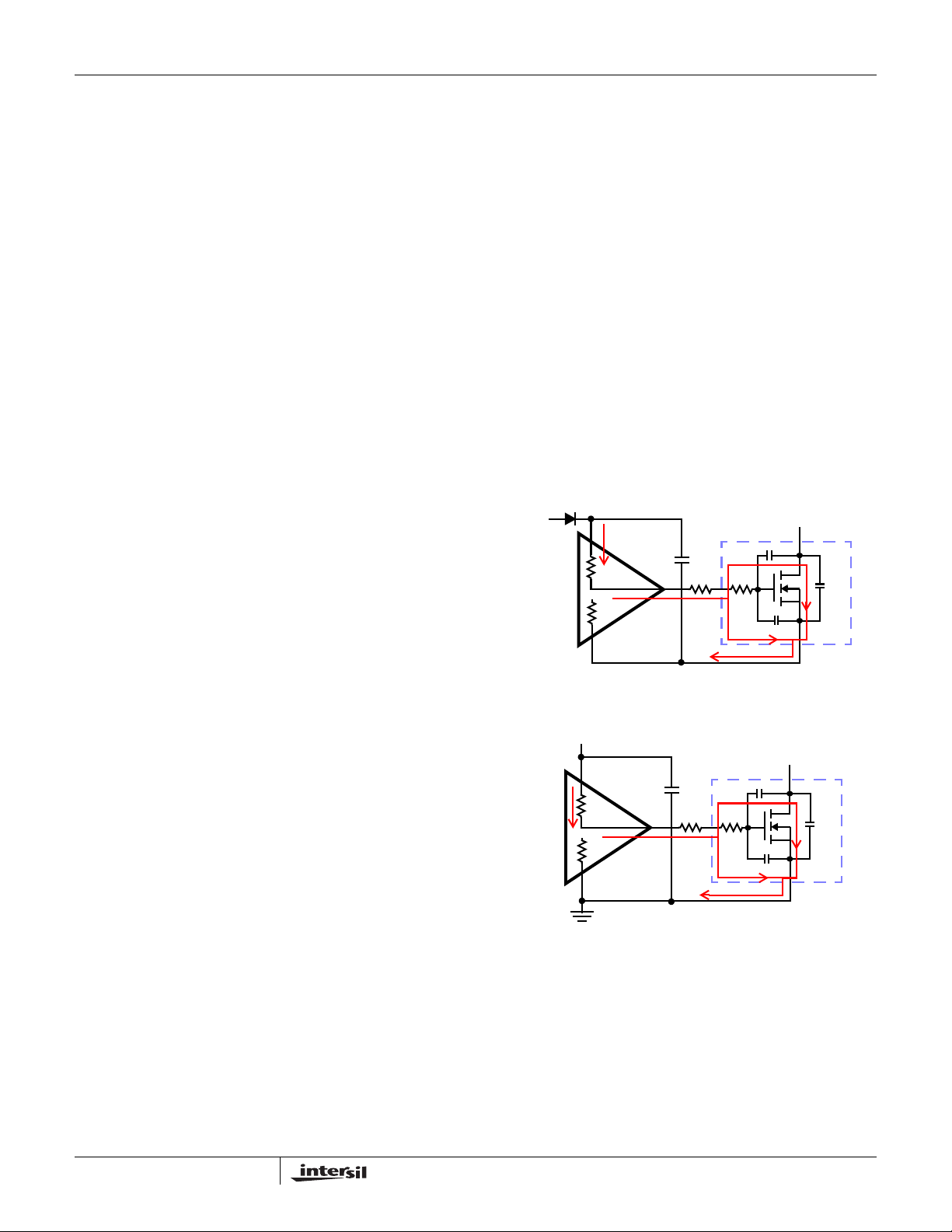
MOSFETs. Figures 3 and 4 show the typical upper and lower
gate drives turn-on transition path. The power dissipation on
the driver can be roughly estimated as:
P
DRPDR_UPPDR _LOWIQ
R
P
DR_UP
P
DR _LOW
R
EXT2RG1
VCC
HI1
--------------------------------------
R
+
HI1REXT1
R
HI2
--------------------------------------
R
+
HI2REXT2
R
GI1
-------------+=
N
Q1
BOOT
R
HI1
R
LO1
UGATE
PHASE
FIGURE 3. TYPICAL UPPER-GATE DRIVE TURN-ON PATH
VCC•++=
R
LO1
----------------------------------------+
R
+
LO1REXT1
R
LO2
----------------------------------------+
R
+
LO2REXT2
R
EXT2RG2
G
R
G1
(EQ. 4)
P
Qg_Q1
---------------------
•=
2
P
Qg_Q2
---------------------
•=
2
R
GI2
-------------+=
N
Q2
D
C
GD
C
DS
R
GI1
C
GS
Q1
S
where the gate charge (Q
particular gate to source voltage (V
corresponding MOSFET datasheet; I
quiescent current with no load at both drive outputs; N
and N
respectively. The I
are the number of upper and lower MOSFETs,
Q2
Q VCC
and QG2) is defined at a
G1
and V
GS1
Q
GS2
is the driver’s total
) in the
Q1
product is the quiescent power of
the driver without capacitive load and is typically negligible.
7
VCC
D
C
LGATE
R
HI2
R
LO2
GND
GD
G
R
GI2
R
G2
C
GS
S
Q2
C
DS
FIGURE 4. TYPICAL LOWER-GATE DRIVE TURN-ON PATH
FN9240.0
November 2, 2005
Page 8
ISL6596
www.BDTIC.com/Intersil
Application Information
MOSFET Selection
The parasitic inductances of the PCB and of the power
devices’ packaging (both upper and lower MOSFETs) can
cause serious ringing, exceeding absolute maximum rating
of the devices. The negative ringing at the edges of the
PHASE node could increase the bootstrap capacitor voltage
through the internal bootstrap diode, and in some cases, it
may overstress the upper MOSFET driver. Careful layout,
proper selection of MOSFETs and packaging can go a long
way toward minimizing such unwanted stress.
2
The D
-PAK, or D-PAK packaged MOSFETs, have large
parasitic lead inductances and are not recommended unless
additional circuits are implemented to prevent the BOOT and
PHASE pins from exceeding the device rating. Low-profile
MOSFETs, such as Direct FETs and multi-SOURCE leads
devices (SO-8, LFPAK, PowerPAK), have low parasitic lead
inductances and are preferred.
Layout Considerations
A good layout helps reduce the ringing on the switching
node (PHASE) and significantly lowers the stress applied to
the output drives. The following advice is meant to lead to an
optimized layout:
• Keep decoupling loops (VCC-GND and BOOT-PHASE) as
short as possible.
• Minimize trace inductance, especially on low-impedance
lines. All power traces (UGATE, PHASE, LGATE, GND,
VCC) should be short and wide, as much as possible.
• Minimize the inductance of the PHASE node. Ideally, the
source of the upper and the drain of the lower MOSFET
should be as close as thermally allowable.
• Minimize the current loop of the output and input power
trains. Short the source connection of the lower MOSFET
to ground as close to the transistor pin as feasible. Input
capacitors (especially ceramic decoupling) should be
placed as close to the drain of upper and source of lower
MOSFETs as possible.
In addition, for heat spreading, place copper underneath the
IC whether it has an exposed pad or not. The copper area
can be extended beyond the bottom area of the IC and/or
connected to buried power ground plane(s) with thermal
vias. This combination of vias for vertical heat escape,
extended copper plane, and buried planes improve heat
dissipation and allow the part to achieve its full thermal
potential.
Upper MOSFET Self Turn-On Effects At Startup
Should the driver have insufficient bias voltage applied, its
outputs are floating. If the input bus is energized at a high
dV/dt rate while the driver outputs are floating, because of
self-coupling via the internal C
UGATE could momentarily rise up to a level greater than the
threshold voltage of the MOSFET. This could potentially turn
on the upper switch and result in damaging inrush energy.
Therefore, if such a situation (when input bus powered up
before the bias of the controller and driver is ready) could
conceivably be encountered, it is a common practice to
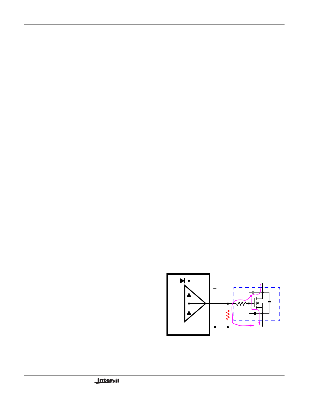
place a resistor (R
) across the gate and source of the
UGPH
upper MOSFET to suppress the Miller coupling effect. The
value of the resistor depends mainly on the input voltage’s
rate of rise, the C
GD/CGS
ratio, as well as the gate-source
threshold of the upper MOSFET. A higher dV/dt, a lower
C
DS/CGS
ratio, and a lower gate-source threshold upper
FET will require a smaller resistor to diminish the effect of
the internal capacitive coupling. For most applications, a
5kΩ to 10kΩ resistor is typically sufficient, not affecting
normal performance and efficiency.
The coupling effect can be roughly estimated with the
following equations, which assume a fixed linear input ramp
and neglect the clamping effect of the body diode of the
upper drive and the bootstrap capacitor. Other parasitic
components such as lead inductances and PCB
capacitances are also not taken into account. These
equations are provided for guidance purpose only.
Therefore, the actual coupling effect should be examined
using a very high impedance (10MΩ or greater) probe to
ensure a safe design margin.
dV
+=
DU
DL
-------
dt
RC
⋅⋅=
rss
C
rssCGD
BOOT
UGATE
PHASE
V
GS_MILLER
RR
UGPHRGI
VCC
ISL6596
of the MOSFET, the
GD
V–
--------------------------- ------ -
dV
-------
⋅
dt
G
UGPH
DS
RC⋅
iss
C
issCGDCGS
C
GD
R
GI
C
GS
(EQ. 5)
+=
VIN
D
C
Q
UPPER
S
1e
–
=
C
BOOT
R
DS
FIGURE 5. GATE TO SOURCE RESISTOR TO REDUCE
8
UPPER MOSFET MILLER COUPLING
FN9240.0
November 2, 2005
Page 9
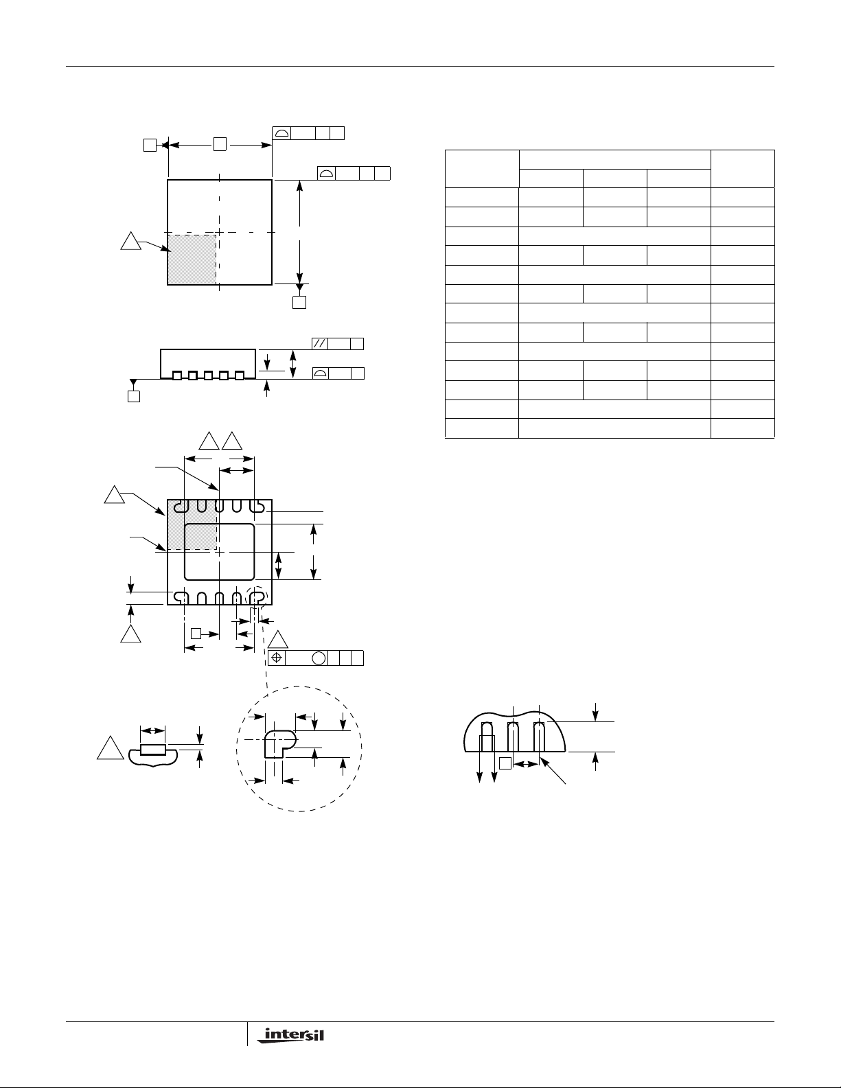
Dual Flat No-Lead Plastic Package (DFN)
www.BDTIC.com/Intersil
ISL6596
INDEX
SEATING
(DATUM B)
6
INDEX
AREA
(DATUM A)
NX (b)
5
SECTION "C-C"
6
AREA
C
PLANE
NX L
8
A
12
D
TOP VIEW
SIDE VIEW
8
7
D2
D2/2
N-1N
e
(Nd-1)Xe
REF.
BOTTOM VIEW
(A1)
2X
A3
NX b
5
0.415
0.15
C
E
B
A
NX
E2
E2/2
0.10 MC
0.200
NX b
C
A
0.152XB
0.10 C
0.08
C
k
AB
NX L
L10.3x3
10 LEAD DUAL FLAT NO-LEAD PLASTIC PACKAGE
MILLIMETERS
C
SYMBOL
A 0.80 0.90 1.00 A1 - - 0.05 A3 0.20 REF -
b 0.18 0.23 0.28 5,8
D 3.00 BSC D2 1.95 2.00 2.05 7,8
E 3.00 BSC E2 1.55 1.60 1.65 7,8
e 0.50 BSC -
k0.25 - - -
L0.300.35 0.40 8
N102
Nd 5 3
NOTES:
1. Dimensioning and tolerancing conform to ASME Y14.5-1994.
2. N is the number of terminals.
3. Nd refers to the number of terminals on D.
4. All dimensions are in millimeters. Angles are in degrees.
5. Dimension b applies to the metallized terminal and is measured
between 0.15mm and 0.30mm from the terminal tip.
6. The configuration of the pin #1 identifier is optional, but must be
located within the zone indicated. The pin #1 identifier may be
either a mold or mark feature.
7. Dimensions D2 and E2 are for the exposed pads which provide
improved electrical and thermal performance.
8. Nominal dimensions are provided to assist with PCB Land
Pattern Design efforts, see Intersil Technical Brief TB389.
C
L
L
e
CC
FOR ODD TERMINAL/SIDE
TERMINAL TIP
NOTESMIN NOMINAL MAX
Rev. 3 6/04
9
FN9240.0
November 2, 2005
Page 10
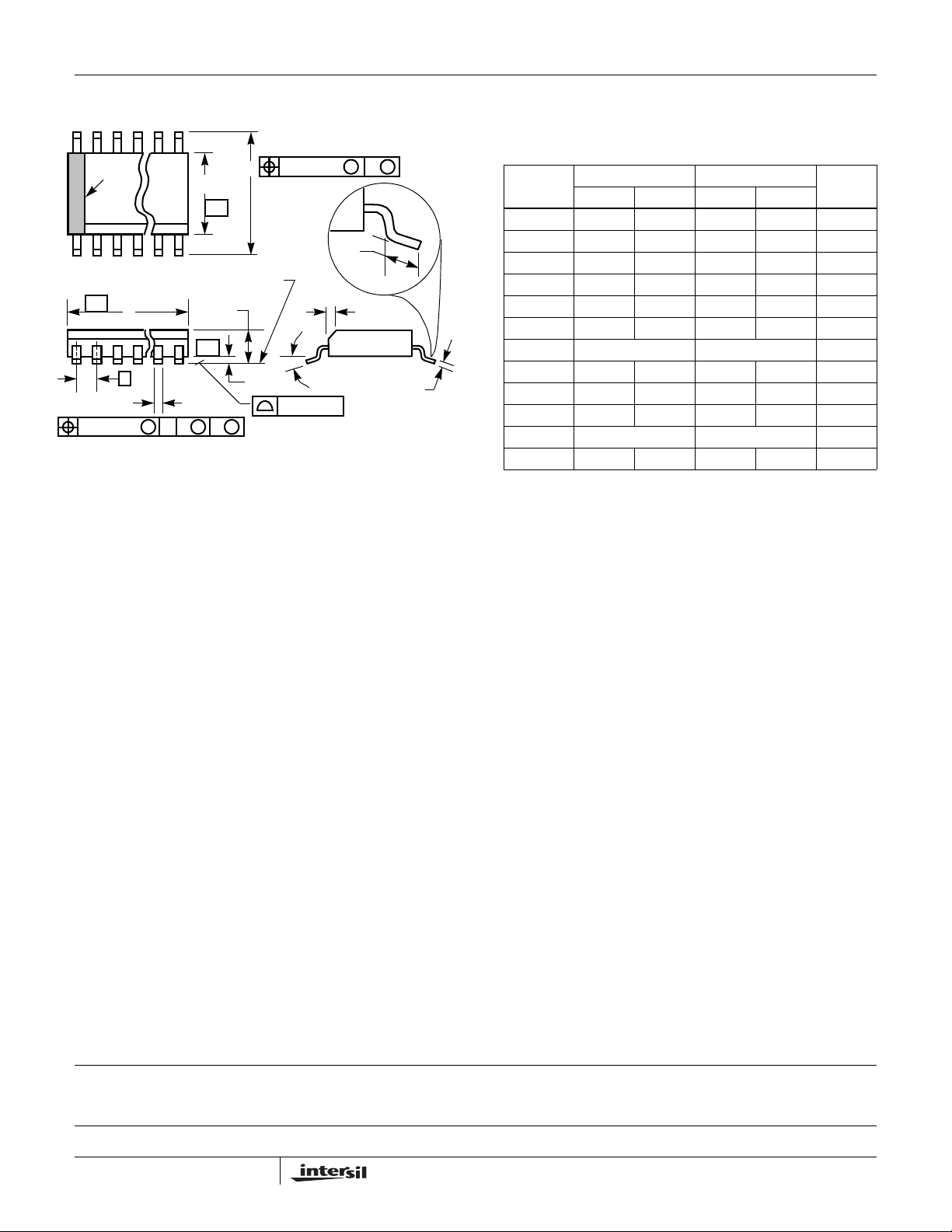
Small Outline Plastic Packages (SOIC)
www.BDTIC.com/Intersil
ISL6596
N
INDEX
AREA
123
-A-
E
-B-
SEATING PLANE
D
A
-C-
0.25(0.010) BM M
H
L
h x 45°
α
e
B
0.25(0.010) C AM BS
NOTES:
1. Symbols are defined in the “MO Series Symbol List” in Section 2.2 of
Publication Number 95.
2. Dimensioning and tolerancing per ANSI Y14.5M-1982.
3. Dimension “D” does not include mold flash, protrusions or gate burrs.
Mold flash, protrusion and gate burrs shall not exceed 0.15mm (0.006
inch) per side.
4. Dimension “E” does not include interlead flash or protrusions. Interlead flash and protrusions shall not exceed 0.25mm (0.010 inch) per
side.
5. The chamfer on the body is optional. If it is not present, a visual index
feature must be located within the crosshatched area.
6. “L” is the length of terminal for soldering to a substrate.
7. “N” is the number of terminal positions.
8. Terminal numbers are shown for reference only.
9. The lead width “B”, as measured 0.36mm (0.014 inch) or greater
above the seating plane, shall not exceed a maximum value of
0.61mm (0.024 inch).
10. Controlling dimension: MILLIMETER. Converted inch dimensions
are not necessarily exact.
M
A1
C
0.10(0.004)
M8.15 (JEDEC MS-012-AA ISSUE C)
8 LEAD NARROW BODY SMALL OUTLINE PLASTIC PACKAGE
INCHES MILLIMETERS
SYMBOL
A 0.0532 0.0688 1.35 1.75 -
A1 0.0040 0.0098 0.10 0.25 -
B 0.013 0.020 0.33 0.51 9
C 0.0075 0.0098 0.19 0.25 D 0.1890 0.1968 4.80 5.00 3
E 0.1497 0.1574 3.80 4.00 4
e 0.050 BSC 1.27 BSC -
H 0.2284 0.2440 5.80 6.20 -
h 0.0099 0.0196 0.25 0.50 5
L 0.016 0.050 0.40 1.27 6
N8 87
α
0° 8° 0° 8° -
NOTESMIN MAX MIN MAX
Rev. 1 6/05
All Intersil U.S. products are manufactured, assembled and tested utilizing ISO9000 quality systems.
Intersil Corporation’s quality certifications can be viewed at www.intersil.com/design/quality
Intersil products are sold by description only. Intersil Corporation reserves the right to make changes in circuit design, software and/or specifications at any time without
notice. Accordingly, the reader is cautioned to verify that data sheets are current before placing orders. Information furnished by Intersil is believed to be accurate and
reliable. However, no responsibility is assumed by Intersil or its subsidiaries for its use; nor for any infringements of patents or other rights of third parties which may result
from its use. No license is granted by implication or otherwise under any patent or patent rights of Intersil or its subsidiaries.
For information regarding Intersil Corporation and its products, see www.intersil.com
10
FN9240.0
November 2, 2005
 Loading...