

Page 1
®
ISL6592
Data Sheet August 5, 2005
6-Phase Digital Multiphase Controller
The ISL6592 digital multiphase controller provides core
power for today's high current microprocessors by driving up
to six synchronous-rectified buck-converter channels in
parallel. Interleaved timing of the channels results in a higher
ripple frequency, reducing input and output ripple. With up to
six phases, each capable of up to 1.5MHz operation, the
ISL6592 can be used to build DC/DC converters that provide
up to 200A with excellent efficiency, low ripple, and the
lowest component count.
The ISL6592 utilizes digital technology to implement all
control functions, providing the ultimate in flexibility and
stability. The ISL6592 incorporates an industry standard I
2
C
serial interface for control and monitoring. Through the serial
interface, the power supply designer can quickly optimize
designs and monitor parameters. The interface allows the
ISL6592 to provide digitized information for real time system
monitoring and control.
The ISL6592 provides superior loadline accuracy through
internal calibration that measures and corrects current sense
error sources upon start-up. The ISL6592 has
programmable current sense temperature compensation
that allows the designer to tailor the response for best
loadline accuracy over temperature. Superior loadline
accuracy reduces component count and solution cost.
To further reduce component count the ISL6592
incorporates patented Active Transient Response (ATR)
technology, allowing the fastest response to transient events
for reduced output capacitance.
The flexibility of the ISL6592 allows the power supply
designer to implement a wide range of solutions. When used
with industry standard power train components, ISL6592
provides the highest performance with lowest component
count and cost. When area is at a premium, ISL6592 can be
used with the ISL6597 integrated power stage to implement
the industry's highest density power solutions.
Ordering Information
TEMP.
PART NUMBER
ISL6592DNZ-T
(Note)
NOTE: Intersil Pb-free plus anneal products employ special Pb-free
material sets; molding compounds/die attach materials and 100% matte
tin plate termination finish, which are RoHS compliant and compatible
with both SnPb and Pb-free soldering operations. Intersil Pb-free
products are MSL classified at Pb-free peak reflow temperatures that
meet or exceed the Pb-free requirements of IPC/JEDEC J STD-020.
RANGE (°C) PACKAGE
0 to 85 48 Ld 7x7 LQFP
(Pb-free)
PKG.
DWG. #
Q48.7x7A
FN9163.1
Features
• Multiphase power conversion
- 2- to 6-phase operation
• 300kHz to 1.5MHz switching frequency
• Supports Intel® VR 10.x, AMD®, and custom VID codes
• Internal high precision voltage reference
- ±5mV voltage setpoint accuracy
• Precision digital current sense calibration
- ±14mV loadline accuracy
• Precise digital current balancing with programmable
offsets for thermal balancing
• Digitally programmable loadline and loop compensation
• Differential voltage sense
• Digital temperature sensor compensation
• Active Transient Response (ATR) enables meeting
transient requirements with reduced output capacitance
2
C interface for monitoring, control and configuration
•I
• Internal non-volatile memory (NVM) to store custom
configurations with four programmable system
configurations
• Extensive fault detection capability with two user
configurable output fault pins
- Input Undervoltage
- Output Under/Overvoltage
- High Side Short
- Per Phase and Total Output Current
- Multiple Internal and External Temperature Limits
- -NVM Configuration
- Calibration Range and Time-Out
• Configurable latched fault or autonomous recovery
shutdown
• Single +3.3V supply operation
• 48 lead LQFP plastic package
• Commercial temperature range of 0°C to 85°C ambient
• Pb-Free Plus Anneal Available (RoHS Compliant)
Applications
• Core power regulation for Intel® and AMD® mprocessors
• Intelligent point-of-load (POL) power regulation
1
CAUTION: These devices are sensitive to electrostatic discharge; follow proper IC Handling Procedures.
1-888-INTERSIL or 1-888-468-3774
| Intersil (and design) is a registered trademark of Intersil Americas Inc.
All other trademarks mentioned are the property of their respective owners.
Copyright Intersil Americas Inc. 2005. All Rights Reserved
Page 2
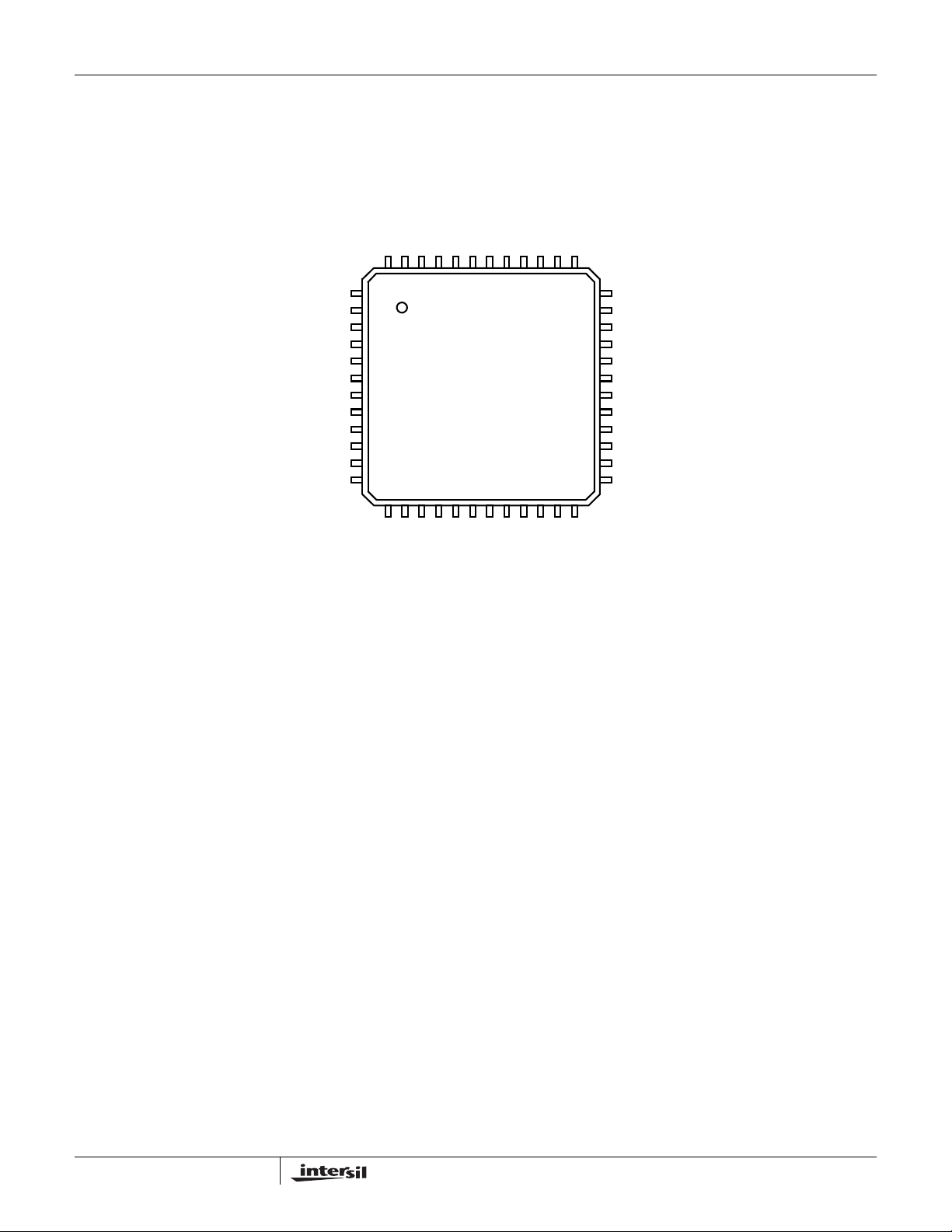
Pinout
ISL6592 (LQFP)
VD25
LL1
LL0
ISL6592
TOP VIEW
SCL
SDA
SADDR
TCLK_SEL
FAULT2
FAULT1
CAL_CUR_EN
CAL_CUR_SEN
RESET_N
GND
VID4
VID3
VID2
VID1
VID0
VID5
OUTEN
VCC_PWRGD
OUT12
OUT11
VDD
4847464544434241403938
1
2
3
4
5
6
7
8
9
10
11
12
1314151617181920212223
OUT9
OUT8
OUT7
OUT6
OUT5
OUT4
OUT10
OUT3
OUT2
OUT1
V12_SEN
37
36
35
34
33
32
31
30
29
28
27
26
25
24
VDD
VDD
ISEN6
ISEN5
ISEN4
ISEN3
ISEN2
ISEN1
TEMP_SEN
VBG_EXT
VSENP
VSENN
GND
2
FN9163.1
August 5, 2005
Page 3
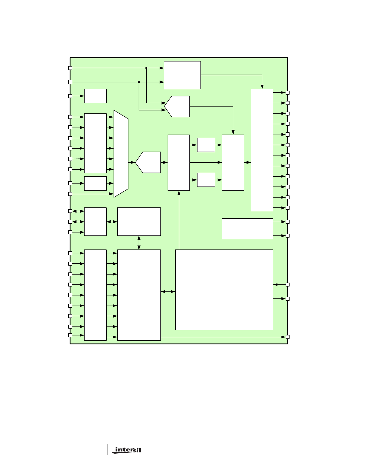
Block Diagram
ISL6592
VSENP
VS ENN
RESET_N
ISEN1
ISEN2
ISEN3
ISEN4
ISEN5
ISEN6
TEMP_SEN
V12_SEN
SCL
SDA
SADDR
POR
Current
Sens e
Current
ADC
Tem p
Sens e
I2C Internal Memory
Window
Com parator
(OVP/UVP)
Voltage
ADC
Channel
Current
Current
Balance
AVP
PID/PWM
Controller
Fault Handler
PWM
Dr ive r
OUT12
OUT11
OUT10
OUT9
OUT8
OUT7
OUT6
OUT5
OUT4
OUT3
OUT2
OUT1
FAULT1
FAULT2
VI D4
VI D3
VI D2
VI D1
VI D0
VI D5
OUTEN
LL0
LL1
Deglitch
Stat e Machine
Dig it al Calib ratio n Controller
FIGURE 1. TOP LEVEL BLOCK DIAGRAM
CAL_CUR_SEN
CAL_CUR_EN
VCC_PWRGD
3
FN9163.1
August 5, 2005
Page 4
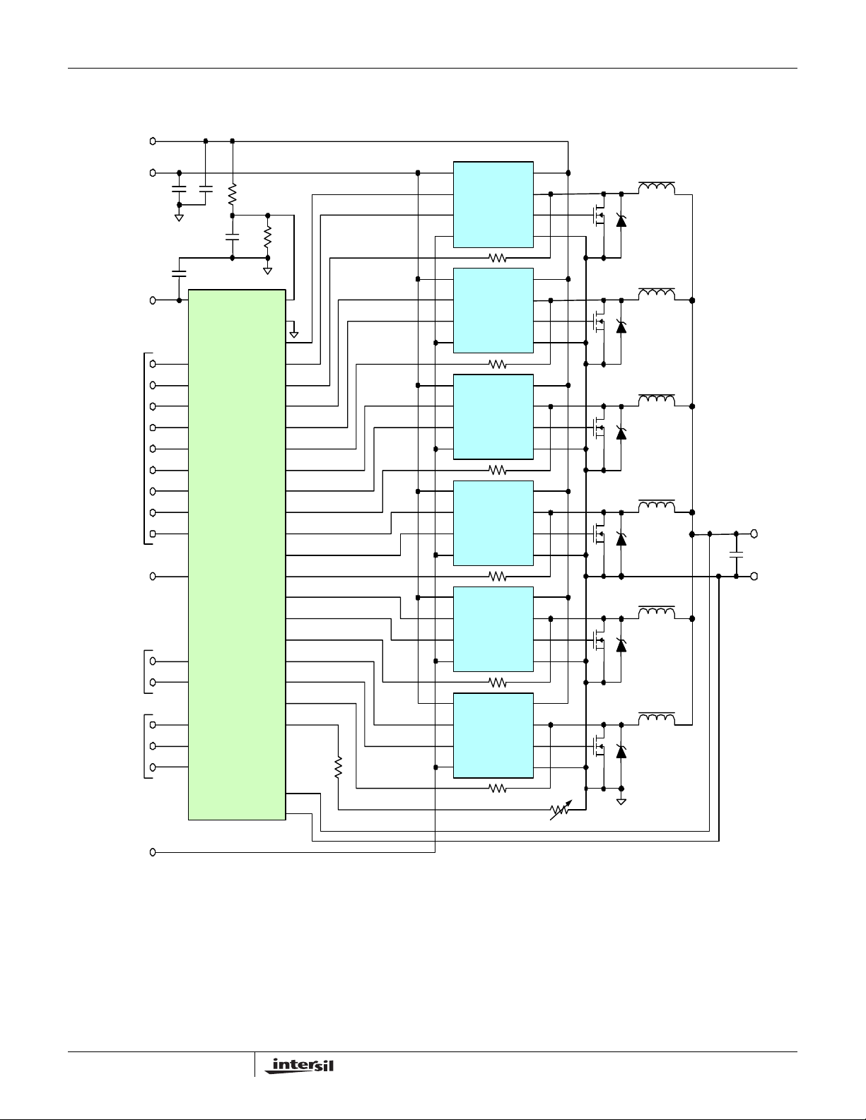
Typical VRM Application
+8V to +12V
ISL6592
+5V to +12V
+3.3V
From
µP
To µP
Fault
Outputs
I2C I/F
Bus
VDD
ISL6592
VID4
VID3
VID2
VID1
VID0
VID5
LL0
LL1
OUTEN
VCC_PWRGD
FAULT1
FAULT2
SDA
SCL
SADDR
CAL_CUR_ SEN
V12_SEN
GND
OUT1
OUT2
ISEN1
OUT3
OUT4
ISEN2
OUT5
OUT6
ISEN3
OUT7
OUT8
ISEN4
OUT9
OUT1 0
ISEN5
OUT1 1
OUT1 2
ISEN6
TEMP_ SEN
CAL_CUR_ EN
VSENP
VSENN
VDRIVE
PWM
NDRIVE
HSS
VDRIVE
PWM
NDRIVE
HSS
VDRIVE
PWM
NDRIVE
HSS
VDRIVE
PWM
NDRIVE
HSS
VDRIVE
PWM
NDRIVE
HSS
VDRIVE
PWM
NDRIVE
HSS
ISL6597
ISL6597
ISL6597
ISL6597
ISL6597
ISL6597
VCC
VSW
NGATE
GND
VCC
VSW
NGATE
GND
VCC
VSW
NGATE
GND
VCC
VSW
NGATE
GND
VCC
VSW
NGATE
GND
VCC
VSW
NGATE
GND
Vout
RTN
RTHERM
Cr owba r
Con tr ol
(optional)
FIGURE 2. 6-PHASE VRM DESIGN WITH ISL6597
4
FN9163.1
August 5, 2005
Page 5
ISL6592
D
Absolute Maximum Ratings Thermal Information
Supply Voltage (VDD) . . . . . . . . . . . . . . . . . . . . . . . -0.50V to 4.25V
All pins except ISENx and ground . . . . . . . . . . . . . . -0.50V to 4.25V
All ISENx pins . . . . . . . . . . . . . . . . . . . . . . . . . . . . . . -0.50V to 3.0V
All ground pins . . . . . . . . . . . . . . . . . . . . . . . . . . . . . -0.50V to 0.50V
Differential Voltage (V
ESD Rating
SEN_DIFF
) . . . . . . . . . . . . . . . . . . . . . . . . 2.5V
Human Body Model (Per MIL-STD-883 Method 3015.7)
(100pF, 1.5kΩ) . . . . . . . . . . . . . . . . . . . . . . . . . . . . . . . . . . 3,000V
Charged Device Model (Per EOS/ESD DS5.3, 4/14/93) . . 1,000V
Machine Model . . . . . . . . . . . . . . . . . . . . . . . . . . . . . . . . . . . .300V
Operating Conditions
Ambient Temperature Range. . . . . . . . . . . . . . . . . . . . . 0°C to 85°C
Supply Voltage Range (Typical). . . . . . . . . . . . . . . . +3.0V to +3.6V
CAUTION: Stresses above those listed in “Absolute Maximum Ratings” may cause permanent damage to the device. This is a stress only rating and operation of the
device at these or any other conditions above those indicated in the operational sections of this specification is not implied.
NOTE:
is measured with the component mounted on a high effective thermal conductivity test board in free air. See Tech Brief TB379 for details.
1. θ
JA
Thermal Resistance (Typical, Note 1) θ
(°C/W)
JA
TQFP Package. . . . . . . . . . . . . . . . . . . . . . . . . . . . . 48
Maximum Storage Temperature Range . . . . . . . . . . . -65°C to 150°C
Maximum Junction Temperature Range . . . . . . . . . . . 0°C to 125°C
Maximum Lead Temperature (Soldering 10s) . . . . . . . . . . . . . 300°C
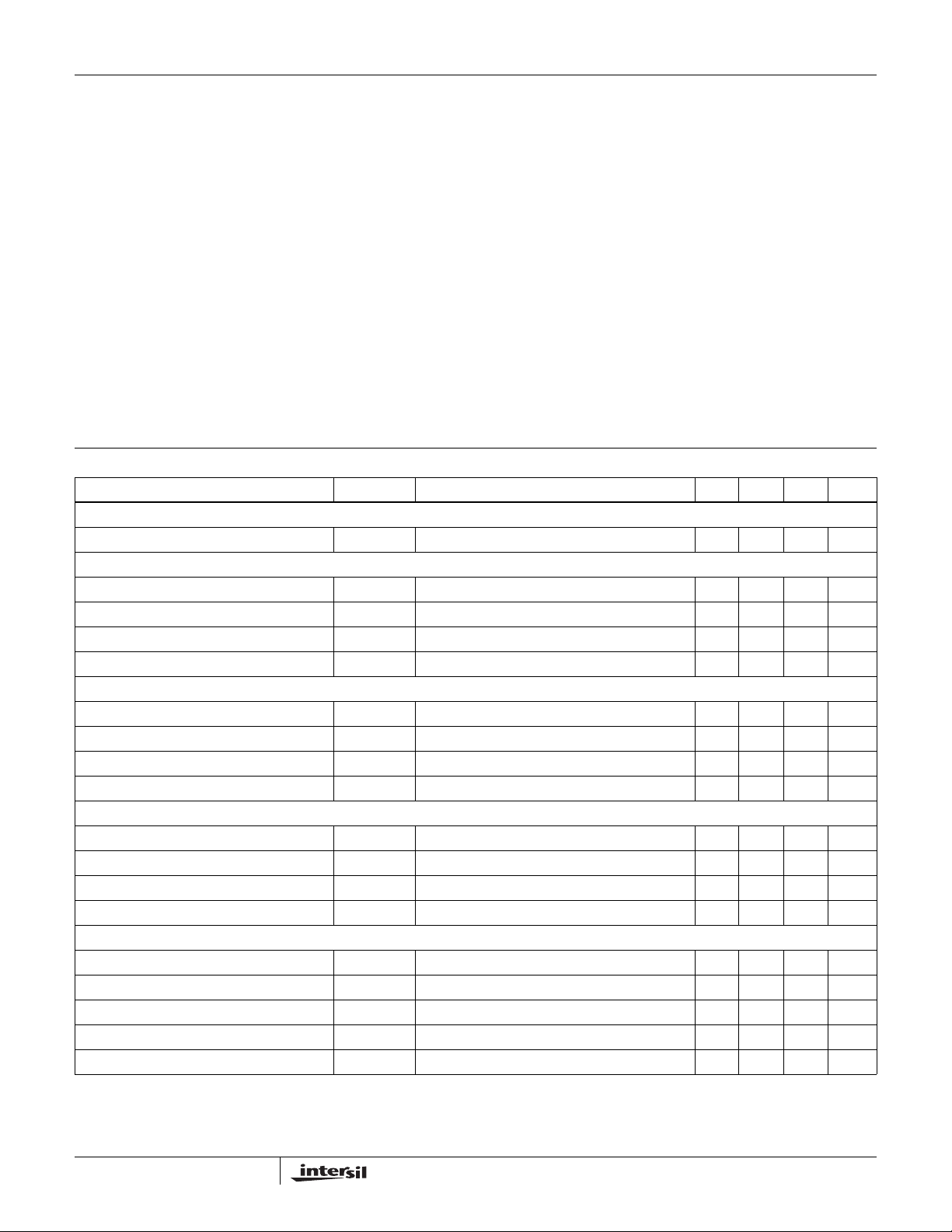
Electrical Specifications V
= +3.3V, TC = +85°C, unless otherwise specified
DD
PARAMETER SYMBOL TEST CONDITIONS MIN TYP MAX UNITS
VDD SUPPLY
Nominal supply current I
VID[5:0] INPUTS (Note 4)
Input low voltage V
Input high voltage V
Input current (input voltage low) I
Input current (input voltage high) I
OUTEN INPUT
Input low voltage V
Input high voltage V
Input current (input voltage low) I
Input current (input voltage high) I
LL[1:0] INPUTS
Input low voltage V
Input high voltage V
Input current (input voltage low) I
Input current (input voltage high) I
SDA, SCL INPUTS
Input low voltage V
Input high voltage V
Input current, input voltage low I
Input current, input voltage high I
Output low voltage V
VDD
IL_VID
IH_VID
IL_VID
IH_VID
IL_OE
IH_OE
IL_OE
IH_OE
IL_LL
IH_LL
IL_LL
IH_LL
IL_S
IH_S
IL_S
IH_S
OL
VDD = +3.3V, ISEN[6:1] = -70µA 100 140 mA
-0.3 0.4 V
(Note 5) 0.8 5.5 V
VIN = 0.0V -75 10 µA
VIN = 3.5V -10 10 µA
-0.3 0.4 V
0.8 5.5 V
OE = 0.0V -75 10 µA
OE = 3.5V -10 10 µA
0.4 V
0.8 V
LL(X) = 0.0V -20 -30 µA
LL(X) = 1.20V 15 25 µA
-0.3 0.8 V
2.4 5.5 V
VIN = 0.0V -10 10 µA
VIN = 3.5V -10 10 µA
Open drain output, I
= +5mA 0.4 V
LOAD
5
FN9163.1
August 5, 2005
Page 6
ISL6592
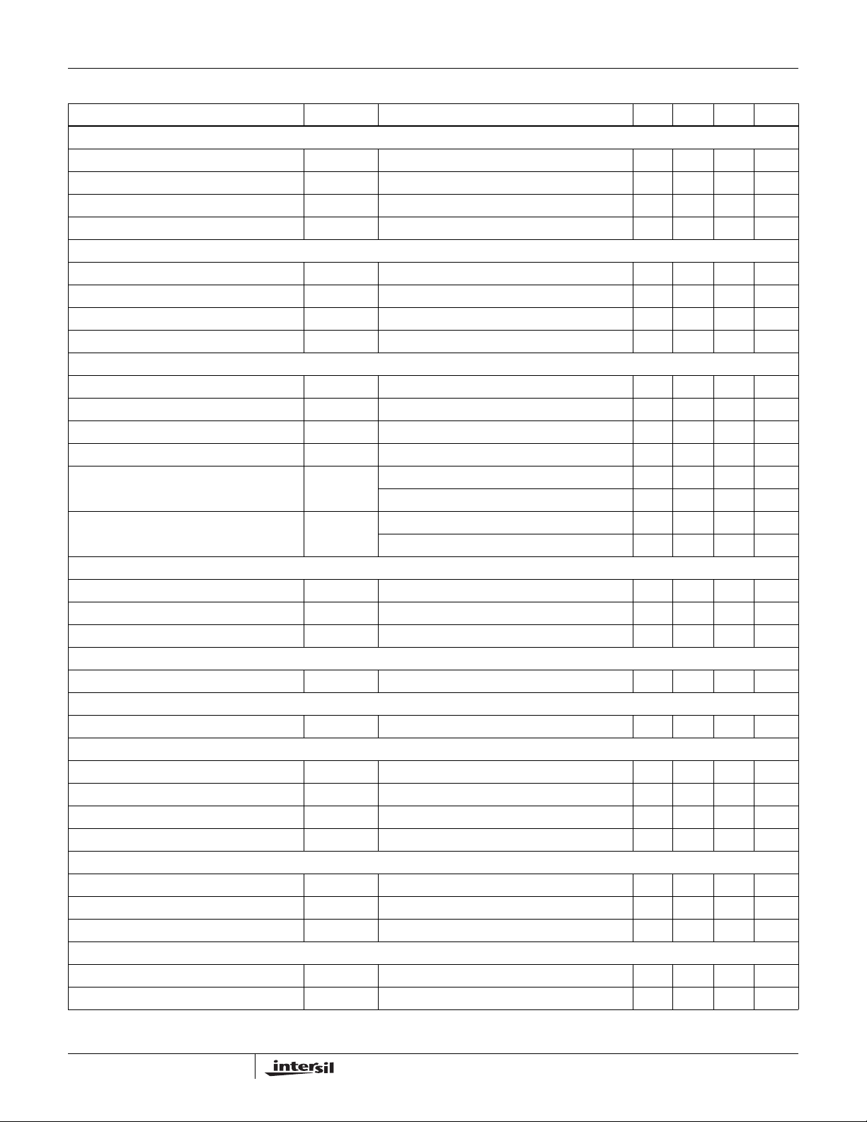
Electrical Specifications V
= +3.3V, TC = +85°C, unless otherwise specified (Continued)
DD
PARAMETER SYMBOL TEST CONDITIONS MIN TYP MAX UNITS
SADDR, RESET_N INPUTS
Input low voltage V
Input high voltage V
Input current, input voltage low I
Input current, input voltage high I
IL_S
IH_S
IL_S
IH_S
VIN = 0.0V -75 -10 µA
VIN = 3.5V -10 10 µA
-0.3 0.5 V
2.8 3.6 V
VSENP, VSENN INPUTS
VSENN voltage V
SENN
(Note 6) ±0.3 V
Bandwidth 1.5 MHz
VSENP input current I
VSENN input current I
IN
IN
VSENP = 1.6V -10 +10 µA
VSENN = 0V -10 +10 µA
ISEN[6:1] INPUTS
Input current range I
IN
-275 -10 µA
Bias voltage accuracy Programmable from 25mV to 150mV -18 +18 mV
Input resistance R
IN
Clamp voltage I
I-Sense amplifier linearity error INL
SA
= 20mA 1.65 V
IN
TA = 25°C 1.6 %
100 Ω
TA = 0 to 85°C, (Note 6) 2 %
Current conversion ADC error INL
IADCTA
= 25°C 2 %
T
= 0 to 85°C, (Note 6) 2.2 %
A
TEMP_SEN INPUT
Bias Voltage V
Input Current Range I
Input resistance R
BIAS
IN
IIN = -20µA 295 mV
-275 -10 µA
IN
200 Ω
V12_SEN INPUT
Voltage threshold V
TH
0.91 1.09 V
CAL_CUR_SEN INPUT
Sensed voltage R
= 20 to 100mΩ, I
SEN
= 2 to 10A 0.17 0.24 V
CAL
RESET_N
Input low voltage V
Input high voltage V
Input current, input voltage low I
Input current, input voltage high I
IL
IH
IL
IH
VIN = 0.0V -75 -10 µA
VIN = 3.5V -10 10 µA
-0.3 0.8 V
2.4 3.6 V
OUT[12:1] OUTPUTS (PWM, NDRIVE)
Output low voltage V
Output high voltage V
Output current, output voltage Hi-Z I
OL
OH
OZ
I
= +5mA 0.4 V
LOAD
I
= -5mA 2.4 V
LOAD
V
= 1.65V -10 10 µA
OUT
FAULT1, FAULT2
Output low voltage V
Output current, output voltage Hi-Z I
OL
OZ
I
= ±5mA 0.4 V
LOAD
V
= 1.65V -10 10 µA
OUT
6
FN9163.1
August 5, 2005
Page 7
ISL6592
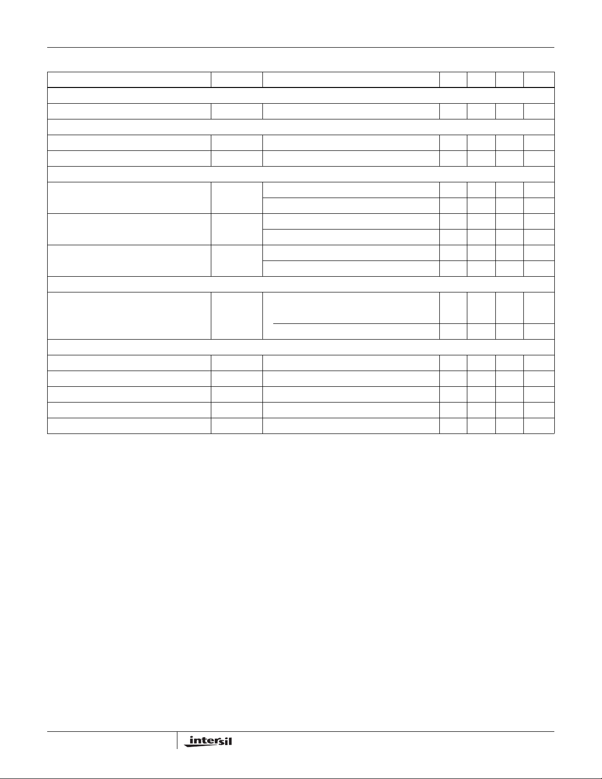
Electrical Specifications V
= +3.3V, TC = +85°C, unless otherwise specified (Continued)
DD
PARAMETER SYMBOL TEST CONDITIONS MIN TYP MAX UNITS
VCC_PWRGD OUTPUT (Note 2)
Output low voltage V
OL
Open drain output, I
= +5mA 0.4 V
LOAD
CAL_CUR_EN
Output low voltage V
Output high voltage V
OL
OH
I
= +500µA 0.4 V
LOAD
I
= -1mA 2.8 V
LOAD
SETPOINT ACCURACY
Setpoint accuracy V
Voltage conversion gain error G
REF
REF
VID = 1.20V, TA = 25°C ±8 mV
VID = 0.85 to 1.60V, T
= 0 to 85°C, (Note 6) ±10 mV
A
TA = 25°C 0.5 %
TA = 0 to 85°C, (Note 6) 0.75 %
Voltage conversion ADC error INL INL
VAD CTA
= 25°C 8.5 mV
T
= 0 to 85°C, (Note 6) 9 mV
A
SWITCHING FREQUENCY
Frequency accuracy F
SW
Range: 100kHz to 2MHz, (Note 7)
T
= 25°C -5 5 %
A
VDD = +3.0V to +3.6V, T
= 0 to 85°C, (Note 6) ±10 %
A
FAULT MONITORS
IUVP lockout threshold (Note 3) V
OUVP threshold voltage (Note 3) V
OOVP threshold accuracy (Note 3) V
IUVP
OUVP
OOVP
0.25V/LSB 2 12 V
0.49 0.60 0.71 V
Programmable from 0.225V to 1.80V (Note 8) -25 +25 mV
Internal OTP threshold range See PTAT shut_down in Table 5
Internal OTP threshold accuracy ±10 °C
NOTES:
2. Open drain output. Contains an active pull-down such that VCC_PWRGD < 0.8V with no +3.3V supplied.
3. Setting is programmable.
4. An open input will float to the logic-1 state. This feature is not intended as a replacement for an external pull-up resistor when the input is driven
by an open-drain driver.
(max) is guaranteed but not tested. Input current is typically less than 2mA at VIH = +5V. In applications requiring +5.5V tolerance, the device
5. V
IH
must be driven by an open drain or open collector source with a pull-up resistance of no less than 1kΩ.
6. Guaranteed, but not tested in production.
7. Setting is programmable.
8. Guaranteed by calibration during production test.
7
FN9163.1
August 5, 2005
Page 8
ISL6592
Pin Description
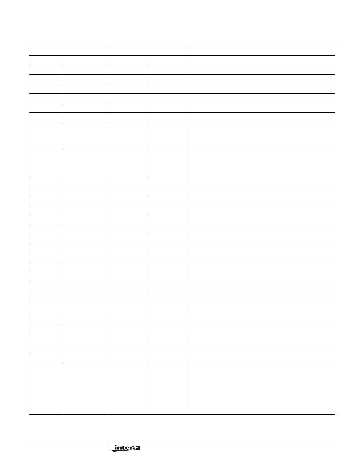
PIN # NAME I/O TYPE DESCRIPTION
1 GND I GND Ground
2 VID4 I 1.2V CMOS Bit 4 of processor voltage identification word (MSB)
3 VID3 I 1.2V CMOS Bit 3 of processor voltage identification word
4 VID2 I 1.2V CMOS Bit 2 of processor voltage identification word
5 VID1 I 1.2V CMOS Bit 1 of processor voltage identification word
6 VID0 I 1.2V CMOS Bit 0 of processor voltage identification word (LSB of 5-bit VID word)
7 VID5 I 1.2V CMOS Bit 5 of processor voltage identification word (LSB of 6-bit VID word)
8 OUTEN I 1.2V CMOS Processor output enable input signal used to command the regulator
9VCC_PWRGD O Open Drain Digital Controller power good control output signal to indicate the
10 OUT12 O 3.3V CMOS Configurable PWM, NDRIVE, ATRH or ATRL output (see Table 3)
11 OUT11 O 3.3V CMOS Configurable PWM, NDRIVE, ATRH or ATRL output (see Table 3)
12 VDD I VDD 3.3V power supply connection
13 OUT10 O 3.3V CMOS Configurable PWM, NDRIVE, ATRH or ATRL output (see Table 3)
14 OUT9 O 3.3V CMOS Configurable PWM, NDRIVE, ATRH or ATRL output (see Table 3)
15 OUT8 O 3.3V CMOS Configurable PWM, NDRIVE, ATRH or ATRL output (see Table 3)
16 OUT7 O 3.3V CMOS Configurable PWM, NDRIVE, ATRH or ATRL output (see Table 3)
17 OUT6 O 3.3V CMOS Configurable PWM, NDRIVE, ATRH or ATRL output (see Table 3)
18 OUT5 O 3.3V CMOS Configurable PWM, NDRIVE, ATRH or ATRL output (see Table 3)
19 OUT4 O 3.3V CMOS Configurable PWM, NDRIVE, ATRH or ATRL output (see Table 3)
20 OUT3 O 3.3V CMOS Configurable PWM, NDRIVE, ATRH or ATRL output (see Table 3)
21 OUT2 O 3.3V CMOS Configurable PWM, NDRIVE, ATRH or ATRL output (see Table 3)
22 OUT1 O 3.3V CMOS Configurable PWM, NDRIVE, ATRH or ATRL output (see Table 3)
23 V12_SEN I Analog 1/10 V12 voltage divider input. Used to guarantee valid input power
24 VDD I VDD 3.3V power supply connection
25 GND I GND Ground
26 VSENN I Analog Negative regulator output voltage sense input.
27 VSENP I Analog Positive regulator output voltage sense input.
28 VBG_EXT I Analog optional external bandgap voltage (not used)
29 TEMP_SEN O Analog External thermistor temperature sense. Connected to ground
output.
“1” Æ Regulator output voltage active
“0” Æ Regulator output voltage three-stated
regulator output voltage is within the specified range.
“1” Æ µP VCC > 90% of target regulation voltage
“0” Æ µP VCC < 90% of target regulation voltage
supply before starting up (undervoltage lockout)
through a negative TC thermistor, with series and shunt resistance
added to achieve desired range. TEMP_SEN is held at 150mV,
current through thermistor is measured by ADC. Effective ADC
range is 0 - 275µA in 4.3µA steps. User should avoid using the 4
codes at the extremes in order to avoid clipping the ADC. ADC code
is translated to temperature using an internal 4 segment piecewise
linear lookup table.
8
FN9163.1
August 5, 2005
Page 9
ISL6592
Pin Description (Continued)
PIN # NAME I/O TYPE DESCRIPTION
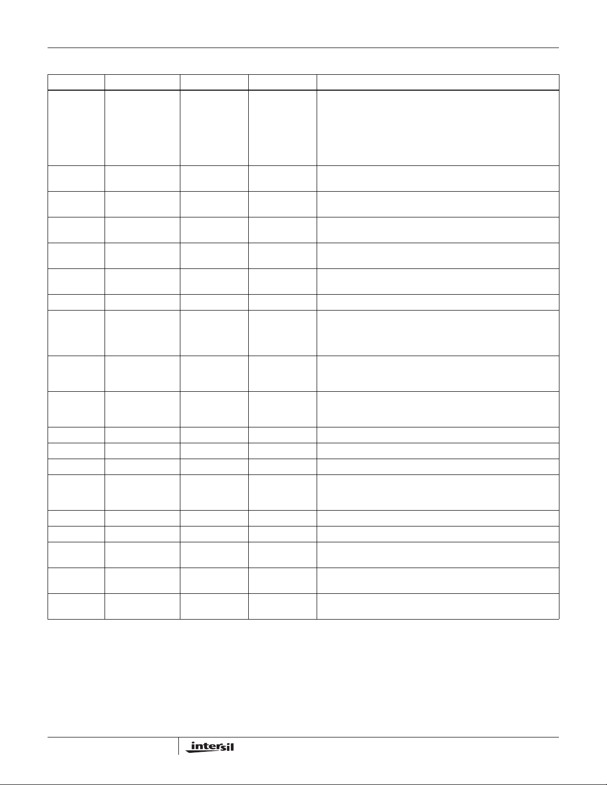
30 ISEN1 I Analog Phase channel #1 ADC current sense input. This pin is held at a
31 ISEN2 I Analog Phase channel #2 ADC current sense input. See ISEN1 for
32 ISEN3 I Analog Phase channel #3 ADC current sense input. See ISEN1 for
33 ISEN4 I Analog Phase channel #4 ADC current sense input. See ISEN1 for
34 ISEN5 I Analog Phase channel #5 ADC current sense input. See ISEN1 for
35 ISEN6 I Analog Phase channel #6 ADC current sense input. See ISEN1 for
36 VDD I VDD 3.3V power supply connection
37 RESET_N I 3.3V CMOS Active low asynchronous system reset to place ISL6592 into default
38 CAL_CUR_SEN I Analog Calibration current sense input. Measures the voltage across the
39 CAL_CUR_EN O Analog Calibration current enable output. Drives the calibration FET gate
40 FAULT1 O 3.3V CMOS Programmable fault indicator #1
41 FAULT2 O 3.3V CMOS Programmable fault indicator #2
42 TCLK_SEL I 3.3V CMOS Tie to Ground for normal operation
43 SADDR I 3.3V CMOS I
44 SDA I 3.3V CMOS I
45 SCL I 3.3V CMOS I2C interface serial clock line.
46 LL0 I 1.2V CMOS Processor load line select input control signal (MSB). Selects
47 LL1 I 1.2V CMOS Processor load line select input control signal (LSB). Selects
48 VD25 I Analog Decoupling capacitor for 2.5V internally generated voltage
virtual ground, with programmable offset from 25 to 300mV. An
external sense resistor is connected to the drain of the low side FET
so that its current may be determined. The current sourced from the
input is given by: ISEN = (Voffset - VRDSON)/RSEN1. Input current
is digitized with the ADC with an effective ADC range of 0 -275µA in
4.3µA steps.
description.
description.
description.
description.
description.
state
“1” Æ asynchronous reset disabled
“0” Æ asynchronous reset enabled
sense resistor. FET gate voltage is adjusted via an opamp loop such
that the voltage across the resistor is set at 100mV.
voltage to adjust its r
resistor is set at 100 mV.
2
C address LSB select
“1” Æ 1110001 selected
“0” Æ 1110000 selected
2
C interface serial data line.
regulator load line resistance.
regulator load line resistance.
0.01µF recommended, 0.1µF max
such that voltage across the sense
DS(ON)
9
FN9163.1
August 5, 2005
Page 10

General Description
The ISL6592 is a digital multi-phase pulse width modulation
controller integrated circuit for use in 2- to 6-phase
synchronous buck converter CPU core supply power
switching regulators. The device is optimized for delivering
voltages from 0.8 to 1.6V at high current levels (120A+) with
programmable PWM switching frequencies between 300kHz
and 1.5MHz. The ISL6592 brings the benefit of digital control
to voltage regulators targeting Intel® VRD/VRM 10.x, AMD®
VRM 1.05, and similar applications.
The ISL6592 is designed to maximize value to the user by
providing features, monitoring and performance to minimize
the number of required off-chip components, work with a
variety of widely available standard components, and to
accommodate wider device tolerance mismatches than
competing analog controller solutions.
The ISL6592 provides both ease-of-use and flexibility to the
user. Major features include:
• Internal Voltage and Temperature Reference - An internal
factory trimmed ±0.5% voltage reference sets the VID
DAC, voltage ADC and current ADC range. In addition, a
proportional-to-absolute-temperature (PTAT) reference is
generated and digitized to serve as the controller
temperature sensor.
• Internal Oscillator - Provides a factory trimmed
156.25MHz ±10% clock reference. Fixed and
programmable dividers generate all the needed internal
clocks to configure the controller's switching frequency
and number of active phases.
• Dedicated Voltage ADC - A high precision differential input
voltage ADC digitizes the differential remote sense
voltage. An integrated anti-alias filter and ripple frequency
null filter minimize the impact of high frequency noise on
the system.
• Multiplexed Current Sense ADC - The average currents
from each phase are sensed as a voltage across the low
side FET using the multiplexed current ADC. Each phase
is sampled at the middle of its cycle, with timing optimized
through a programmable delay line. The internal
temperature reference and external thermistor
temperature are also digitized using the multiplexed
current ADC. Gain and offset of the sensor and ADC are
compensated through either a one time factory calibration,
or through a power-up calibration each time the output
voltage is reset.
• Digital Control Loop and AVP - An over-sampled digital
Proportional-Integral-Derivative (PID) compensator
provides flexible loop compensation with programmable
coefficients. A digital post-filter provides additional phase
lead and/or high frequency filtering to optimize the
transient response and ripple of the system. A high
accuracy Active Voltage Positioning (AVP) loadline is
ISL6592
computed using the calibrated current sense
measurements. The AVP bandwidth is also programmable
to allow it to be optimized for dynamic performance.
• Window comparators - Window comparators with
programmable thresholds to be set for overvoltage
protection (OOVP) and high side short (HSS) detection.
• Active Transient Response (ATR) - ATR comparators with
programmable thresholds are used to provide fast
response to dynamic load transients, minimizing spike
overshoot and droop undershoot.
• Configurable PWM Generators - 2-6 PWM waveforms are
digitally generated ensuring low jitter and high linearity.
PWM outputs are configurable as either single tri-valent
outputs or dual outputs with programmable non-overlap
delay. Phases can be fully overlapped, with programmable
duty cycle limiting.
• Integrated NVM - Digital configuration is stored in an
integrated NVM, allowing fully independent (stand-alone)
operation. NVM is fully accessible to user so that a
completely new parameter set can be written. Vendor and
user defined memory locations are provided, allowing
version control and part identification. NVM integrity is
checked every configuration cycle through a cyclic
redundancy check (CRC) comparison.
• Serial Interface - GUI software provides easy access to all
configuration, telemetry, and testability features over a 2
2
wire I
C serial interface.
The GUI interface allows full accessibility to regulator
telemetry during system operation including:
• Internal Controller Temperature
• External (via optional thermistor) System Temperature
• Per Phase Current
• Total Output Current
• Output Voltage
• Input Voltage
• Configurable latched and unlatched individual fault status
• Microprocessor Leakage Current
• User defined memory space
Fault reporting and shutdown behavior are also fully
configurable. Two individual fault outputs are provided, with
all faults being independently maskable. The outputs can be
configured as either latched or unlatched, active high or
active low polarity, and CMOS or open drain outputs. The
shutdown operation also allows all faults to be individually
masked and for the shutdown operation to be either latched
or unlatched. Individual status registers allow fault reporting
10
FN9163.1
August 5, 2005
Page 11

ISL6592
over the serial bus to identify the specific fault event. Fault
detection includes the following:
• Input Undervoltage
• Output Overvoltage
• Output Undervoltage
• High-side Short
• Per Phase Overcurrent
• Total Output Overcurrent
• Two levels of Internal Temperature Protection
• Two levels of External Temperature Protection
• Configuration Failure
• Calibration Range Failure
• Calibration Time-out Failure
The ISL6592 is also optimized for use with the ISL6597
integrated power stage to deliver a high performance VR
solution. The ISL6597 offers the following benefits when
combined with the ISL6592 controller:
• Low delay, fast transition, low r
high side P-channel FET
• Low delay, high drive (2A) low side N-channel FET driver
• High accuracy, low drift integrated current mirror, allowing
lossless current sensing with loadline accuracy
comparable to series sense resistor solutions
• Power supply sequence independence between the
power input (12V), low side driver supply (5-12V), and
controller supply (3.3V)
• Direct high side short detect and crowbar capability,
operates off the 12V input supply and is thus independent
of controller power supply
Please see the ISL6597 data sheet for more details on the
performance, capability, and interface requirements of
ISL6592/ISL6597 systems.
(13mΩ) integrated
DS(ON)
Theory of Operation
may be low, high or three-state. During the inactive state, the
controller can communicate over the serial bus, report
configuration or inactive state faults (e.g. high side short).
The controller will leave the inactive state and begin softstart once it has a valid VID, OEN is asserted, and the 12V
power input is valid. The 12V input is sensed through a
resistive divider on the board, and a programmable
threshold comparator must be tripped if the input
undervoltage lockout is enabled. The sense circuit can be
easily modified to also sense an independent or sequenced
lower drive voltage typically used to optimize the efficiency of
the power stage low side FET.
Soft-Start and Calibration
Prior to entering an active regulating state, the ISL6592
performs a well-controlled, monotonic initial ramp or "softstart". Soft-start is performed by actively regulating the load
voltage while digitally ramping the target voltage from 0 to
the voltage set. During this time, the optional power-up
system calibration can be performed. The calibration
algorithm compensates for variations in low-side FET
r
a low voltage level, putting a known current load through
each phase individually and compensating for the current
sense gain and offset error, as well as changes in
temperature. Alternatively, default compensation values can
be used, or the compensation values can be computed
during system test and stored in memory. The external
current load needed to perform calibration can be
implemented with a precision resistor and N-channel FET.
The voltage across the resistor is sensed and the N-channel
FET gate voltage is adjusted through an internal opamp loop
to provide the desired precision current. The calibration
current level and the voltage level at which the calibration is
performed are both programmable.
After the soft-start ramp is completed, the processor's
leakage current is measured. At this point the regulator
enters the active regulation state and the VCC_PWRGD pin
transitions from "0" to "1," indicating that the microprocessor
voltage is within 90% of the target value.
, parasitic inductance and resistance by regulating to
DS(ON)
Power Up and Initialization
The ISL6592 is designed to provide supply sequence
independence and graceful turn-on and turn-off operation. It
operates from a single +3.3V supply, while an on-chip low
drop-out (LDO) regulator generates an internal +2.5V
supply. Power-up controller configuration is initialized by
either an internal threshold based power-on reset, or by an
external reset pin (RST_N). During controller configuration,
the contents of the NVM are read into the controller's
registers. During configuration, all outputs are three-stated,
allowing board pull-up or pull-down resistors to set the
correct default level.
Once configuration is completed, the controller enters an
inactive state. Outputs assume their default values, which
11
FN9163.1
August 5, 2005
Page 12
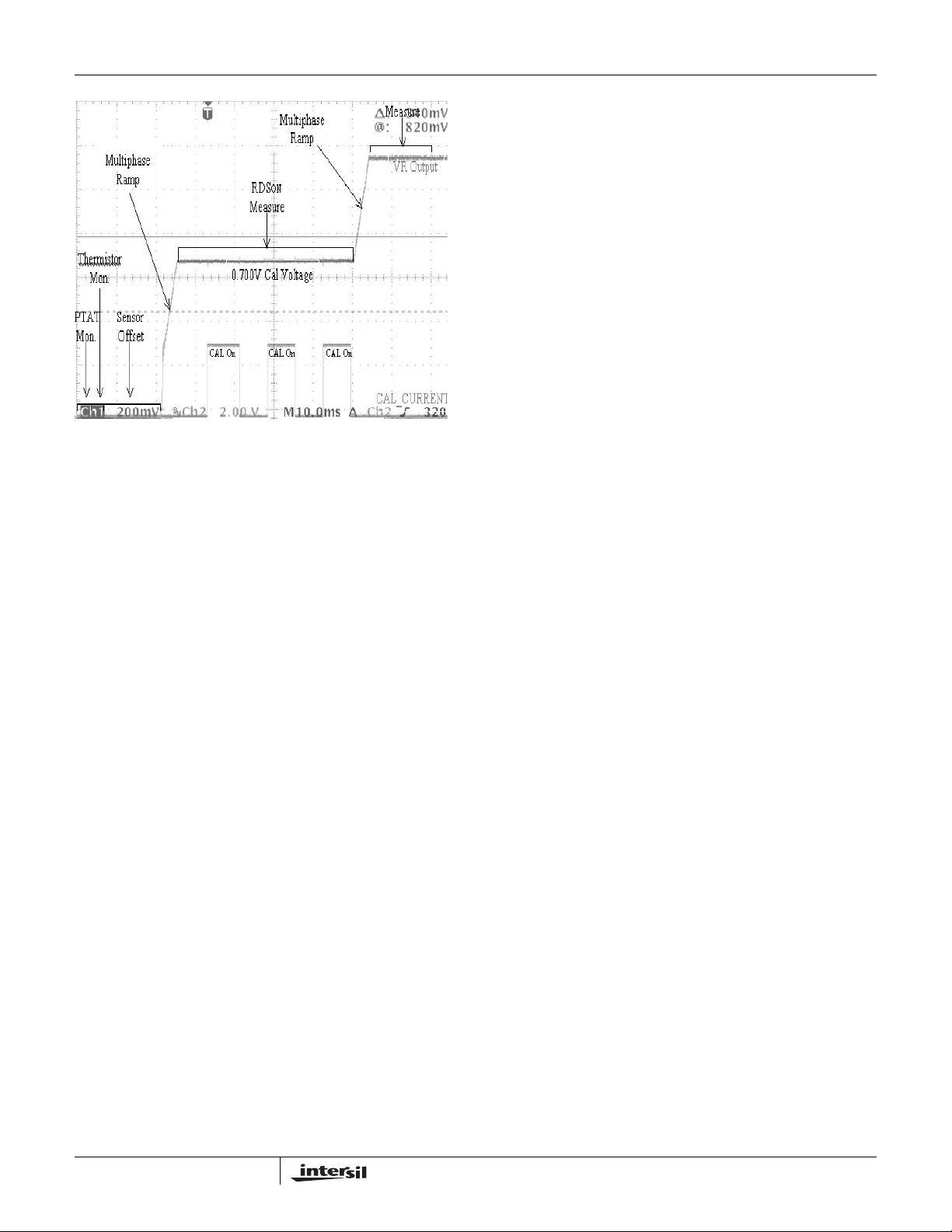
FIGURE 3. SOFT-START/CALIBRATION SEQUENCE
(3-PHASE)
ISL6592
is the programmable divider ratio between 6 and 127, and
Nph is the number of phases between 2 and 6.
Although switching frequencies of less than 300kHz and
greater than 1.5MHz can be generated, various system
optimization parameters may not have adequate range to
optimize the loop outside this range.
Output Voltage Sensing and Voltage ADC
The ISL6592 is built around a high performance digital
feedback control loop that senses the differential voltage at
the load. This is used to generate the appropriate pulse
width modulated (PWM) waveforms to drive the power
stages and regulate the load voltage.
The differential sense voltage is digitized with a high speed,
high precision analog-to-digital converter (ADC). The onchip factory trimmed temperature compensated bandgap
voltage reference ensures the ADC accuracy is well within
the regulator setpoint accuracy requirements. The ADC is
sampled synchronously so that there are 2 ADC samples
per phase per switching cycle, at a frequency given by:
Shutdown
The ISL6592 also performs a controlled shutdown response
to minimize any voltage undershoot. The shutdown state can
be entered from the soft-start or active regulation states
either through user intervention (de-asserting OEN or all
one's VID), or through a detected fault such as overtemperature or output overvoltage. During shutdown, the
PWM width is reduced at a steady programmable rate, and
then the power stage is three-stated once the pulse width
reaches 0.
After shutdown is complete, the controller re-enters the
inactive state after a fixed delay. This delay minimizes the
duty cycle associated with autonomous restarts if the fault
that caused the shutdown disappears once the output is
disabled. Alternatively, the fault can be configured so that it
is latched and clearing requires user intervention such as
toggling OEN, toggling RESET_N, or cycling power.
Switching Frequency
Timing is provided by an on-chip, factory trimmed,
temperature compensated oscillator. Additionally, this onchip oscillator can be frequency modulated by a pseudo
random pattern to spread the clock spectrum and reduce
system electro-magnetic interference (EMI).
The ISL6592 operates with a fixed switching frequency (i.e.
the switching frequency is fixed independent of load) that is
configurable between 300kHz and 1.5MHz. A programmable
divider is used to generate the switching frequency, where
the frequency is given by:
Fsw = 156.25MHz/(2 x div_sel x Nph)
where Fsw is the switching frequency, 156.25MHz is the
nominal frequency of the timing reference oscillator, div_sel
Fs = 156.25MHz/div_sel
The ADC also includes a post-filter which, when enabled,
provides a null at Fsw * (Nph/2), which is the ripple
frequency. This ripple null filter works in conjunction with an
internal analog anti-alias filter. The anti-alias filter is a single
pole, 2MHz low pass filter. The corner frequency can be
lowered by adding series resistors in the board.
Current Sensing and Current ADC
The ISL6592 provides for precise current monitoring in each
power stage, allowing for industry-leading loadline accuracy
for active voltage positioning (AVP). The current in each
power stage is sensed by measuring the voltage across the
bottom side FET in the middle of its on cycle. This voltage is
digitized using a multiplexed current ADC.
The current sense inputs (ISEN1 to ISEN6) are held at a
virtual ground with programmable offset from 25mV to
200mV. The large voltage swing at the drain of the low side
FET is eliminated by using a series resistor, converting the
signal to a current equal to:
Isense = (Voff - Vds)/Rsense
where Isense is the current sourced by the sense input, Voff
is the programmable offset, Vds is the voltage across the low
side FET, and Rsense is an external resistor whose value is
chosen to scale the input depending on the expected
r
The input current is mirrored and multiplexed, then digitized
by the 6 bit current ADC with an effective input range of 0 to
275µA in 4.3µA steps. The ADC samples the current in each
phase once per switching cycle, and the sampling instant
can be varied using a programmable delay, such that
sampling in the middle of the ON cycle can be guaranteed.
DS(ON)
.
12
FN9163.1
August 5, 2005
Page 13

ISL6592
The current in the power stage can then be inferred from the
current ADC measurement if the drain-source resistance
(r
) of the FET is known. The r
DS(ON)
DS(ON)
of each FET
can be either programmed as a default value, or it can be
determined by running the calibration routine either one time
at system test or every time the system starts up. Calibration
is performed by providing a known current load while the
regulator is on and correcting the gain and offset of the
current measurement. This requires the use of a precision
external current source consisting of a dedicated calibration
FET and sense resistor. The ISL6592 senses the voltage
across the resistor and provide a variable voltage to drive
the gate of the calibration FET, varying its r
DS(ON)
such that
the current through the FET and resistor are under closed
loop control. The calibration current and voltage level at
which calibration occurs are programmable, and the
calibration routine can be bypassed if the default values are
to be used. The r
value is compensated for
DS(ON)
temperature drift using either the on-chip temperature sense
or an external thermistor that can be placed close to the
power stage.
The external temperature sense input, TEMP_SEN, is a
virtual ground input with a fixed offset of 150mV. An external
negative TC thermistor is tied to ground, generating the input
current for the measurement. Series resistors or shunt
resistors can be used to scale the current. The current range
is the same as the current sense inputs, from 0 to 275µA in
4.3µA steps. Default values should be chosen such that the
ADC range is not clipped. The ADC measurements are
converted to temperature using a programmable 4-segment
piece-wise linear table. The internal proportional-to-absolute
temperature (PTAT) reference is digitized directly, using a
linear curve fit. Both internal and external temperature
measurements are multiplexed through the current ADC at a
low frequency, providing run-time internal and external
temperature information to perform temperature
compensation, reporting, alerts, and shutdown.
When used with the ISL6597 integrated power stage, the
integrated current sense output can be directly interfaced
with the ISL6592 current sense input. The integrated current
sense provides superior accuracy, with loadline accuracy
comparable to those achieved with series sense resistors.
Additionally, the integrated temperature sense in the
ISL6597 can be used instead of the external thermistor,
providing direct power stage measurements to the system.
Digital Control Loop and PWM Generation
The digital control loop uses a proportional, integral, and
derivative (PID) compensator to drive the digitized sense
voltage to the desired target. An additional second derivative
gain term and a 2nd order post-filter provide additional high
order zeros and poles to further refine the wideband
characteristics of the loop. All loop parameters are
programmable over a wide range of values, allowing loop
bandwidths of 10-300kHz to be attained depending on the
number and type of power stages used.
The effective transfer function of the compensator is given
by:
K
i
Hz()
----------------- - K
=
1K
++
----------------------------------------------------------++
1K
fd1
++ +
1z1––
fd1Kfd2
z1–K
fd2
1z1––()Kd21z1––()
pKd
K
mod
-----------------------------------
2–
Nphdiv_sel⋅
z
V
--------
2
in
Q
where:
Ki, Kp, Kd, and Kd2 are the integral, proportional,
derivative, and second derivative gain terms
Kfd1 and Kfd2 are the coefficients of a second order all
pole low pass post-filter
Kmod is a programmable maximum duty cycle scaling
term
Nph is the number of phases and div_sel is the divider
ratio setting the switching frequency
Vin is the power stage input voltage, typically 12V
Q is the ADC step size, 3.125mV
The control loop operates at the same frequency as the
voltage ADC, which is synchronous to the switching
frequency and given by:
Fs = 2 * Nph * Fsw = 156.25MHz/div_sel
The compensator digital output is converted to a pulse width
using a digital counter based pulse width modulator. The
pulse width modulator uses 2 successive samples to
modulate the leading edge and then the trailing edge of a
pulse. The modulator provides for monotonic edge
placements with a resolution of 100ps. The next 2 samples
are then used to modulate the next phase in the firing
sequence. The pulse width modulator is capable of setting a
maximum duty cycle limit, overlapping adjacent phases, a
minimum pulse width of 13ns, and also producing zero pulse
width with minimal glitching.
Voltage Identification Codes
The target voltage is provided by external parallel 6-bit
voltage identification (VID) inputs. The VID maps can be
configured as either Intel® VID, AMD®, or programmable
offset tables. The ISL6592 is fully compliant with VRD/VRM
10.1 and 10.2 deglitching and dynamic VID stepping
requirements.
13
FN9163.1
August 5, 2005
Page 14

ISL6592
TABLE 1. OUTPUT VOLTAGE vs INTEL® VID CODES
VID4 VID3 VID2 VID1 VID0 VID5 VOUT VID4 VID3 VID2 VID1 VID0 VID5 VOUT
0 1 0 1 0 0 0.8375 1 1 0 1 0 0 1.2125
0 1 0 0 1 1 0.8500 1 1 0 0 1 1 1.2250
0 1 0 0 1 0 0.8625 1 1 0 0 1 0 1.2375
0 1 0 0 0 1 0.8750 1 1 0 0 0 1 1.2500
0 1 0 0 0 0 0.8875 1 1 0 0 0 0 1.2625
0 0 1 1 1 1 0.9000 1 0 1 1 1 1 1.2750
0 0 1 1 1 0 0.9125 1 0 1 1 1 0 1.2875
0 0 1 1 0 1 0.9250 1 0 1 1 0 1 1.3000
0 0 1 1 0 0 0.9375 1 0 1 1 0 0 1.3125
0 0 1 0 1 1 0.9500 1 0 1 0 1 1 1.3250
0 0 1 0 1 0 0.9625 1 0 1 0 1 0 1.3375
0 0 1 0 0 1 0.9750 1 0 1 0 0 1 1.3500
0 0 1 0 0 0 0.9875 1 0 1 0 0 0 1.3625
0 0 0 1 1 1 1.0000 1 0 0 1 1 1 1.3750
0 0 0 1 1 0 1.0125 1 0 0 1 1 0 1.3875
0 0 0 1 0 1 1.0250 1 0 0 1 0 1 1.4000
0 0 0 1 0 0 1.0375 1 0 0 1 0 0 1.4125
0 0 0 0 1 1 1.0500 1 0 0 0 1 1 1.4250
0 0 0 0 1 0 1.0625 1 0 0 0 1 0 1.4375
0 0 0 0 0 1 1.0750 1 0 0 0 0 1 1.4500
0 0 0 0 0 0 1.0875 0 0 0 0 0 0 1.4625
1 1 1 1 1 1 OFF 0 1 1 1 1 1 1.4750
1 1 1 1 1 0 OFF 0 1 1 1 1 0 1.4875
1 1 1 1 0 1 1.1000 0 1 1 1 0 1 1.5000
1 1 1 1 0 0 1.1125 0 1 1 1 0 0 1.5125
1 1 1 0 1 1 1.1250 0 1 1 0 1 1 1.5250
1 1 1 0 1 0 1.1375 0 1 1 0 1 0 1.5375
1 1 1 0 0 1 1.1500 0 1 1 0 0 1 1.5500
1 1 1 0 0 0 1.1625 0 1 1 0 0 0 1.5625
1 1 0 1 1 1 1.1750 0 1 0 1 1 1 1.5750
1 1 0 1 1 0 1.1875 0 1 0 1 1 0 1.5875
1 1 0 1 0 1 1.2000 0 1 0 1 0 1 1.6000
14
FN9163.1
August 5, 2005
Page 15

ISL6592
TABLE 2. OUTPUT VOLTAGE vs AMD® VID CODES
VID4 VID3 VID2 VID1 VID0 VID5 VOUT VID4 VID3 VID2 VID1 VID0 VID5 VOUT
0 1 0 1 0 X 1.3000 1 1 0 1 0 X 0.9000
0 1 0 0 1 X 1.3250 1 1 0 0 1 X 0.9250
0 1 0 0 0 X 1.3500 1 1 0 0 0 X 0.9500
0 0 1 1 1 X 1.3750 1 0 1 1 1 X 0.9750
0 0 1 1 0 X 1.4000 1 0 1 1 0 X 1.0000
0 0 1 0 1 X 1.4250 1 0 1 0 1 X 1.0250
0 0 1 0 0 X 1.4500 1 0 1 0 0 X 1.0500
0 0 0 1 1 X 1.4750 1 0 0 1 1 X 1.0750
0 0 0 1 0 X 1.5000 1 0 0 1 0 X 1.1000
0 0 0 0 1 X 1.5250 1 0 0 0 1 X 1.1250
0 0 0 0 0 X 1.5500 1 0 0 0 0 X 1.1500
1 1 1 1 1 X OFF 0 1 1 1 1 X 1.1750
1 1 1 1 0 X 0.8000 0 1 1 1 0 X 1.2000
1 1 1 0 1 X 0.8250 0 1 1 0 1 X 1.2250
1 1 1 0 0 X 0.8500 0 1 1 0 0 X 1.2500
1 1 0 1 1 X 0.8750 0 1 0 1 1 X 1.2750
Active Voltage Positioning (AVP)
The AVP loadline can be selected from 4 pre-programmed
values using the VRD/M 10.x compliant load line select (LL1
and LL0) inputs. This allows selection of both the loadline
slope and the VID setpoint offset. The loadline slope is
selectable from 0 to 4mΩ, and the setpoint offset is
selectable from 0 to 50mV in 1.56mV steps.
The total current is computed by adding the current
measured from each phase, then filtering with a single pole
programmable filter to set the AVP bandwidth.
Current Balancing/Thermal Balancing
The ISL6592 also uses the channel current measurements
to perform current balancing. To minimize thermal gradient
effects, each channel adaptively adjusts its current to match
the average channel current.
The current balance function can also be used to induce a
thermal gradient if, for example, some channels have
greater cooling capability due to better proximity to airflow.
The ISL6592 allows the user to independently force an offset
current to each channel, creating a current gradient. This
causes the current balance to force the channels with
greater cooling capability to supply a higher percentage of
the total current, creating a net thermal equilibrium amongst
all channels.
Active Transient Response (ATR)
Active Transient Response (ATR) is supported through loadline tracking comparators with programmable thresholds.
Both internal- and external-loop ATR are supported. Internalloop ATR engages multiple phases to maximize output
current slew rate and minimize spike and droop due to large
transient events. Three independent window comparators
allows for variation in the number of phases that sink or
source. If the transient is slight, only one phase will respond.
If the transient is severe, up to three phases respond. This
avoids a dramatic sinking or sourcing event, which can
cause oscillation. The ISL6592 controller itself uses
hysteretic control algorithms after the transient event to
ensure that the power stages return to normal operation
smoothly with minimal ringing. External-loop ATR provides
additional outputs to engage an additional low latency power
stage capable of quick charge delivery to the load. This
consists of a small FET with a very fast gate driver. Internaland external-loop ATR can be used independently or in
conjunction to optimize transient performance.
Output Configurations
The ISL6592 provides 12 configurable outputs that are used
to drive up to 6 phase power stages. The outputs can be
configured as a single tri-valent pulse width modulated
(PWM) signal, or as dual complementary high side control
(PWM) and low side control (NDRIVE). In addition, the
outputs may also be configured to provide the ex-loop ATR
outputs, ATRH to drive a high side undershoot control FET,
and ATRL to drive a low side overshoot control FET.
For single output configurations, tri-valent FET drivers must
be used. The driver input circuit has two thresholds (upper
and lower) along with a bias network such that its input is
centered between the two thresholds when the ISL6592
output driver is three-stated. This allows three values to be
defined for the signal, depending whether the output is high,
15
FN9163.1
August 5, 2005
Page 16
ISL6592
low, or high impedance. If the input signal is high, the gate
driver turns the high-side switch on. If the input signal is low,
the gate driver turns the low-side switch on. If the input
signal is three-state, the driver does not turn either high-side
or low-side switches on and the power stage is high
impedance or three-stated. Non-overlap circuitry matched to
the switch FETs characteristics must be incorporated in the
FET driver.
For dual output configurations, two independent driver
circuits are implemented for the high side and low side.
Three-stating the output stage only requires both the PWM
and NDRIVE signals to be held logic low. ISL6592
separate rising edge and falling edge delays, so that the dual
driver does not require non-overlap logic.
The output drive signals are generated using a 3.3V trivalent driver. All outputs are three-stated during reset,
configuration, and inactive state. This allows the user to set
the appropriate level to three-state the power stage, using
external pull-up or pull-down resistors. ISL6592 also
supports independent polarity control on each output,
allowing any polarity driver to be used.
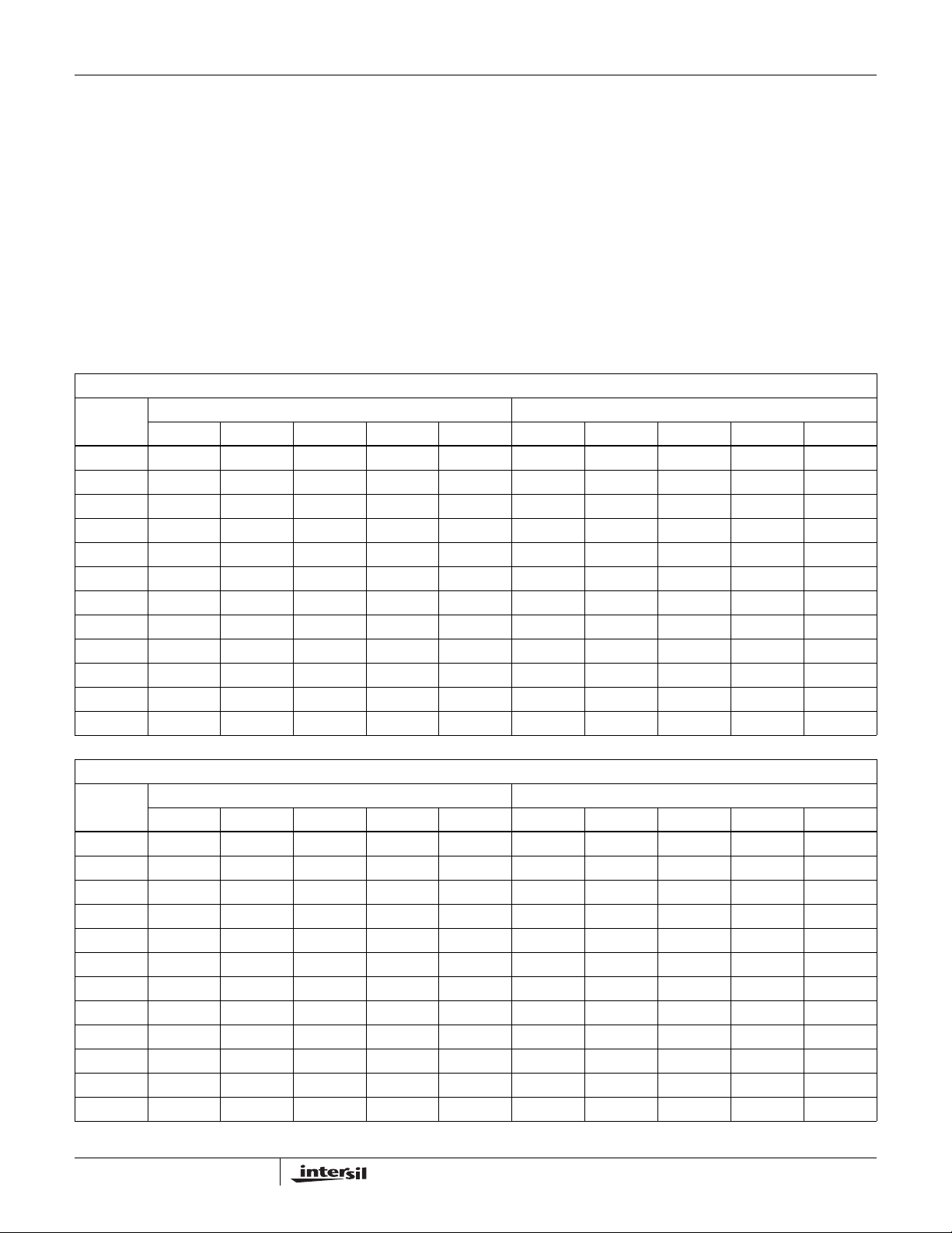
ISL6592 supporst various output configurations as shown in
the Table 3 below.
incorporates programmable non-overlap delay, with
TABLE 3. PROGRAMMABLE OUTPUT CONFIGURATION
NON-SCRAMBLED OUTPUTS (pwm_scramble = 0)
# OF PHASES FOR SINGLE PWM OUTPUTS (dual = 0) # OF PHASES FOR DUAL PWM/NDRIVE OUTPUTS (dual = 1)
OUT
[1] pwm1 pwm1 pwm1 pwm1 pwm1 pwm1 pwm1 pwm1 pwm1 pwm1
[2] pwm2 pwm2 pwm2 pwm2 pwm2 pwm2 pwm2 pwm2 pwm2 pwm2
[3] hi-Z pwm3 pwm3 pwm3 pwm3 hi-Z pwm3 pwm3 pwm3 pwm3
[4] hi-Z hi-Z pwm4 pwm4 pwm4 ndr1 ndr1 ndr1 ndr1 ndr1
[5] hi-Z hi-Z hi-Z pwm5 pwm5 ndr2 ndr2 ndr2 ndr2 ndr2
[6] hi-Z hi-Z hi-Z hi-Z pwm6 hi-Z ndr3 ndr3 ndr3 ndr3
[7] hi-Z (atrh) hi-Z (atrh) hi-Z (atrh) hi-Z (atrh) hi-Z (atrh) hi-Z (atrh) hi-Z (atrh) pwm4 pwm4 pwm4
[8] hi-Z (atrl) hi-Z (atrl) hi-Z (atrl) hi-Z (atrl) hi-Z (atrl) hi-Z (atrl) hi-Z (atrl) ndr4 ndr4 ndr4
[9] hi-Z hi-Z hi-Z hi-Z hi-Z hi-Z hi-Z hi-Z (atrh) pwm5 pwm5
[10] hi-Z hi-Z hi-Z hi-Z hi-Z hi-Z hi-Z hi-Z (atrl) ndr5 ndr5
[11] hi-Z hi-Z hi-Z hi-Z hi-Z hi-Z hi-Z hi-Z hi-Z (atrh) pwm6
[12] hi-Z hi-Z hi-Z hi-Z hi-Z hi-Z hi-Z hi-Z hi-Z (atrl) ndr6
2345623456
SCRAMBLED OUTPUTS (pwm_scramble = 1)
# OF PHASES FOR SINGLE PWM OUTPUTS (dual = 0) # OF PHASES FOR DUAL PWM/NDRIVE OUTPUTS (dual = 1)
OUT
[1] pwm1 pwm1 pwm1 pwm1 pwm1 pwm1 pwm1 pwm1 pwm1 pwm1
[2] hi-Z hi-Z pwm4 pwm4 pwm4 ndr1 ndr1 ndr1 ndr1 ndr1
[3] pwm2 pwm2 pwm2 pwm2 pwm2 pwm2 pwm2 pwm2 pwm2 pwm2
[4] hi-Z hi-Z hi-Z pwm5 pwm5 ndr2 ndr2 ndr2 ndr2 ndr2
[5] hi-Z pwm3 pwm3 pwm3 pwm3 hi-Z pwm3 pwm3 pwm3 pwm3
[6] hi-Z hi-Z hi-Z hi-Z pwm6 hi-Z ndr3 ndr3 ndr3 ndr3
[7] hi-Z (atrh) hi-Z (atrh) hi-Z (atrh) hi-Z (atrh) hi-Z (atrh) hi-Z (atrh) hi-Z (atrh) pwm4 pwm4 pwm4
[8] hi-Z (atrl) hi-Z (atrl) hi-Z (atrl) hi-Z (atrl) hi-Z (atrl) hi-Z (atrl) hi-Z (atrl) ndr4 ndr4 ndr4
[9] hi-Z hi-Z hi-Z hi-Z hi-Z hi-Z hi-Z hi-Z (atrh) pwm5 pwm5
[10] hi-Z hi-Z hi-Z hi-Z hi-Z hi-Z hi-Z hi-Z (atrl) ndr5 ndr5
[11] hi-Z hi-Z hi-Z hi-Z hi-Z hi-Z hi-Z hi-Z hi-Z (atrh) pwm6
[12] hi-Z hi-Z hi-Z hi-Z hi-Z hi-Z hi-Z hi-Z hi-Z (atrl) ndr6
2345623456
16
FN9163.1
August 5, 2005
Page 17

ISL6592
Output Firing Sequence
The PWM output and current sense (ISEN) pins of the
ISL6592 have been assigned such they can be placed
sequentially for PC board layouts (i.e. phase 2 next to 1, phase
3 next to 2, etc...). The output phases are set in a pre-wired
firing order to facilitate layout of high phase count systems.
For high phase count systems, the VRD layout in the
motherboard will likely require the power components to be
laid out across two sides of the processor. The firing
sequence shown in the table below ensures that for a highly
distributed power array, the maximum spatial distribution can
be obtained between sequential phases.
TABLE 4. OUTPUT FIRING SEQUENCE
φ FIRING SEQUENCE
21 Æ 2 Æ 1 Æ 2 Æ 1 Æ 2 Æ 1 Æ 2 Æ 1 Æ 2 Æ 1 Æ 2 ...
31 Æ 2 Æ 3 Æ 1 Æ 2 Æ 3 Æ 1 Æ 2 Æ 3 Æ 1 Æ 2 Æ 3 ...
41 Æ 4 Æ 2 Æ 3 Æ 1 Æ 4 Æ 2 Æ 3 Æ 1 Æ 4 Æ 2 Æ 3 ...
51 Æ 4 Æ 2 Æ 5 Æ 3 Æ 1 Æ 4 Æ 2 Æ 5 Æ 3 Æ 1 Æ 4 ...
61 Æ 4 Æ 2 Æ 5 Æ 3 Æ 6 Æ 1 Æ 4 Æ 2 Æ 5 Æ 3 Æ 6 ...
Fault Detection and Fault Handling
The ISL6592 provides a very flexible fault detection reporting
and handling mechanism. Fault detection capability
includes:
• Input Undervoltage Protection (IUVP)
• Output Overvoltage Protection (OOVP)
• Output Undervoltage Protection (OUVP)
• High-side Short (HSS)
• Per Phase Overcurrent Protection (OCP)
• Total Output Overcurrent
• Two levels of Internal Temperature Protection
• Two levels of External Temperature Protection
• Configuration Failure
• Calibration Range Failure
• Calibration Time-out Failure
All individual faults are latched and reported over the serial
interface. Two configurable fault outputs are provided. Each
output allows independent masking of all faults, allowing a
subset of faults to be reported over that pin. The outputs can
also be configured as either latched or unlatched, active high
or active low polarity, and CMOS or open drain outputs.
Typical usage of the configurable fault pins would be as a
crowbar signal to drive an external crowbar device,
temperature alert to notify the system a thermal shutdown is
imminent, or as an interrupt to cause a micro-controller to
poll the fault registers.
Shutdown operation also allows a subset of faults to be
individually masked. Additionally, the shutdown recovery can
be either autonomous or latched. For autonomous recovery,
the faults are not latched, so if the fault condition is
eliminated when the controller returns to an inactive state, it
will wait for a programmable time period, and then attempt a
new soft-start. If the fault condition reoccurs, the controller
will recommence the shutdown sequence, continuing this
cycle indefinitely until the fault condition is eliminated. The
programmable delay ensures a sufficiently low duty cycle to
prevent the regulator components from being damaged from
power cycling, assuming the fault condition itself is not
immediately destructive.
For latched shutdown, user intervention to clear the latched
fault is required before a new soft-start can be attempted.
User intervention must come in the form of OUTEN toggle,
RESET_N toggle, or controller power cycle.
In addition to fault reporting, there are additional fault
handling capabilities specific to each fault type that attempts
to provide more graceful fault handling than a shutdown, but
more active than simply reporting. The specific fault
detection capability and alternate fault handling capability is
as follows:
IUVP: The V12_SEN input continuously senses the +12V
supply through a nominally 10:1 resistive divider. A
comparator with a programmable threshold is used to
indicate an undervoltage condition. IUVP can be used to
independently provide either an undervoltage lockout prior to
soft-start, or to both provide a lockout and force a shutdown
during active regulation.
OOVP/OUVP: Programmable comparators continuously
monitor the VSEN inputs to detect an output overvoltage or
undervoltage condition. The voltage threshold is set relative
to VID. OOVP is enabled during soft-start and active
regulation, while OUVP is enabled only during active
regulation.
HSS: The HSS (high-side short) comparator monitors the
power stages switch node through the ISEN inputs during
the inactive state. If a voltage above 1.0V is detected, the
comparator will indicate a HSS detect. If enabled, this will
turn all the low side FETs on and prevent the controller from
beginning the start-up process. The HSS comparators are
disabled in soft-start and active regulation.
OCP: The OCP (overcurrent protection) continuously
monitors all channel currents to determine whether any of
the currents are greater than a programmable threshold.
Two mechanisms work independently to control overcurrent
conditions. A cycle-by-cycle current limit operates by
disabling a channel for one cycle when its current exceeds
the threshold. A second mechanism monitors the average
current for an overcurrent condition. A programmable
threshold sets a current limit at which a steeper loadline is
implemented, quickly reducing the output voltage downward
17
FN9163.1
August 5, 2005
Page 18

ISL6592
as the current increases. Both of these mechanisms allow
hiccup mode overcurrent protection, where the controller
continues to try to provide a regulated output voltage while in
overcurrent. Alternatively, a threshold can be set where the
overcurrent condition will cause the controller to initiate
shutdown.
Over-Temperature Alert/Shutdown: Both the internal and
external temperature monitors are able to provide fault
telemetry in order to shut down the VR in an overtemperature condition. Two programmable thresholds are
available for temperature faults. Crossing of the first
threshold can be used to only generate a fault report.
Crossing the second threshold can be used to cause a
shutdown to occur.
CRC Failure: The integrity of loading the configuration from
the NVM to the controller's registers is checked through a
cyclic redundancy code (CRC) check of the data contents. A
CRC failure prevents the controller from leaving the inactive
state.
Calibration Failure: Calibration failures can be detected as
either out of range parameter computations or inability to
achieve a regulation target in the given time-frame. These
failures typically indicate a component is damaged or
missing.
I2C Interface
All operating parameters in the ISL6592 is configurable via
2
the I
C interface. Status can also be read back via the same
interface. The ISL6592 operates as a slave at a standard
speed of 100kHz.
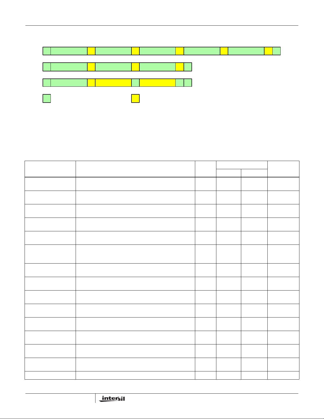
Three transactions are supported on the I
current address, 2) Write register, 3) Read register from
current address.
All transactions start with a control byte sent from the I
master device. The control byte begins with a Start condition,
followed by 7-bits of slave address. The last bit sent by the
master is the R/W bit and is 0 for a write. If any slaves on the
2
I
C bus recognize their address, they will Acknowledge by
pulling the serial data line low for the last clock cycle in the
control byte. If no slaves exist at that address or are not
ready to communicate, the data line will be 1, indicating a
Not Acknowledge condition. The ISL6592 address on the
2
I
C bus is 1110_000 or 1110_001, with the LSB set by the
input pin SADDR.
2
C interface: 1) Set
2
C
The master then sends a byte representing the data LS-byte
to be written at the current address. The ISL6592 will
respond with an Acknowledge. The master then issues a
Stop condition, indicating to the ISL6592 that the current
transaction is complete.
To set the current 16-bit address in the ISL6592, the master
sends a control byte with the R/W bit set to 0, indicating a
write. If it receives an Acknowledge from the ISL6592, it
sends a byte representing the address MS-byte. The
ISL6592 will respond with an Acknowledge. The master then
sends a byte representing the address LS-byte. The
ISL6592 will respond with an Acknowledge. The master then
issues a Stop condition, indicating to the ISL6592 that the
current transaction is complete. Any read commands issued
to the ISL6592 will return data from this address.
To read a register from the ISL6592, the master first sets the
address to read from. It then sends a control byte with the
R/W bit set to 1, indicating a read. If it receives an
Acknowledge from the ISL6592 it sends 8 clocks but does
not drive the serial data line. The ISL6592 will respond with
the MS-byte at the current address. The master will respond
with an Acknowledge to indicate to the ISL6592 that the
transaction is not yet complete. The master again sends 8
clocks but does not drive the serial data line. The ISL6592
will respond with the LS-byte at the current address. The
master will respond with a Not Acknowledge to indicate to
the ISL6592 that the transaction is complete. The ISL6592
will stop driving the serial data line. The master then issues a
Stop condition to indicate that the transaction is complete.
If the ISL6592 has started an internal operation in response
to a transaction on the I
2
C bus (register read/write, flash
write, flash page erase) but the operation has not completed
before the last Acknowledge slot in the I
2
C bus protocol, the
ISL6592 will add wait states by stretching the low portion of
the last clock cycle. This also occurs in response to
read/write requests to addresses that do not support
physical memory in the ISL6592. In this case, the ISL6592
will add wait states until an internal watchdog timer expires,
and the I
2
C bus is guaranteed to be released.
To write a register in the ISL6592, the master sends a control
byte with the R/W bit set to 0, indicating a write. If it receives
an Acknowledge from the ISL6592, it sends a byte
representing the address MSB. The ISL6592 will respond
with an Acknowledge. The master then sends a byte
representing the address LSB. The ISL6592 will respond
with an Acknowledge. The master then sends a byte
representing the data MS-byte to be written at the current
address. The ISL6592 will respond with an Acknowledge.
18
FN9163.1
August 5, 2005
Page 19
ISL6592
I2C Read and Write Protocol
Data write
S slav e_ad d r + W A reg_addr MSB A reg_addr LSB A reg_data MSB reg_data LSBA A P
Set c ur r ent address
S slav e_ad d r + W A reg_addr MSB A reg_addr LSB A P
Read fr om c ur r ent address
S slave_add r + R A reg_addr MSB reg_addr LSB PA N
Dr i ven by master Dr i ven by s lave
Key Registers
Table 5 below provides brief descriptions of several key
configuration (R/W - read/write) and status (RO - read only)
registers available on the ISL6592 Digital Multiphase
Controllers.
TABLE 5. KEY REGISTERS
RANGE
REGISTER DESCRIPTION FORMAT
isum_avg[18:0] VR load current. Averaged sum of all channel current data over
a user programmable averaging window (default = 16ms)
vavp_avg_mon[9:0] AVP output voltage. Averaged VAVP monitored value ADC
voltage.
kavp_XX[9:0] AVP loadline slope. Nominal value of load line slope resistance
input for case LL1 = X, LL0 = X.
load_line_offset_XX[4:0] AVP loadline VID offset. VID set-point load-line offset tolerance
voltage for case LL1 = X, LL0 = X.
kavp_limit_XX[9:0] Secondary overcurrent limit AVP loadline slope. Overcurrent
load line slope resistance input for case LL1 = X, LL0 = X.
isum_max_XX[7:0] Overcurrent limit. Max load current threshold for secondary
slope roll-off of AVP voltage or overcurrent shutdown for case
LL1 = X, LL0 = X.
ptat_mon[5:0] PTAT Temperature. Averaged PTAT calibration temperature
output.
ptat_alert_ref[5:0] PTAT alert temperature. PTAT sensor alert temperature
reference.
ptat_shutdown_ref[5:0] PTAT shutdown temperature. PTAT sensor shutdown
temperature reference.
temp_mon[5:0] Thermistor temperature. Averaged Thermistor monitor
temperature output.
therm_alert_ref[5:0] Thermistor alert temperature. Thermistor sensor alert
temperature reference.
therm_shutdown_ref[5:0] Thermistor shutdown temperature. Thermistor sensor
shutdown temperature reference.
iuvp_thresh[5:0] Input undervoltage threshold. IUVP comparator threshold fixed
at 0.975V
oovp_limit_XX[5:0] Output overvoltage protect threshold. Tracking VID overvoltage
threshold for case LL1 = X, LL0 = X.
ouvp_limit_XX[5:0] Output undervoltage protect threshold fixed at 0.6V R/W n/aV 600mV 12.5mV
RO 0.00A 524.288A 1mA
RO 0.0mV 3,196.875mV 3.125mV
R/W 0.0Ω 3.902mΩ 0.003815mΩ
R/W 0.0V 48.4375mV 1.5625mV
R/W 0.0Ω 15.610mΩ 0.01526mΩ
R/W 0.0A +204.0A 0.800A
RO 0°C 157.5°C 2.5°C
R/W 0°C 157.5°C 2.5°C
R/W 0°C 157.5°C 2.5°C
RO 0°C 157.5°C 2.5°C
R/W 0°C 157.5°C 2.5°C
R/W 0°C 157.5°C 2.5°C
R/W n/a .975V 0.25V
R/W 0.0mV 787.5mV 12.5mV
RESOLUTIONMIN MAX
19
FN9163.1
August 5, 2005
Page 20

ISL6592
TABLE 5. KEY REGISTERS
REGISTER DESCRIPTION FORMAT
pwm_scramble PWM scramble select. Controls mapping of PWM and NDRIVE
dual PWM/NDRIVE select.
fault1_mask[17:0]
fault2_mask[17:0]
shutdown_mask[15:0] Shutdown control mask. Inputs are enabled for shutdown when
ch_mask[6:1] Channel mask. Selects number of active phases. Phases must
signals to pins OUT1 through OUT12. See Table 3 herein for
details.
0 = Only PWM outputs active for use with single input drivers
1 = PWM & NDRIVE outputs active for use with dual input
drivers
Fault1 pin output masks. Inputs are enabled for reporting when
set to logic 1. If multiple inputs are selected, output is “OR” of
selected input signals.
17 = NVM fault
16 = Internal bus fault
15 = IUVP
14 = OUVP
13 = OOVP
12 = thermistor temp alert
11 = thermistor temp shutdown
10 = PTAT temp alert
9 = PTAT temp shutdown
8 = channel 1 high side short
7 = channel 2 high side short
6 = channel 3 high side short
5 = channel 4 high side short
4 = channel 5 high side short
3 = channel 6 high side short
2 = unused
1 = MHz controller fault
0 = Calibration fault
set to logic 1. If multiple inputs are selected, output is “OR” of
selected input signals.
15 = IUVP
14 = OUVP
13 = OOVP
12 = Individual phase current fault during active regulation
11 = thermistor temp shutdown
10 = Individual phase current fault during soft-start
9 = PTAT temp shutdown
8 = channel 1 high side short
7 = channel 2 high side short
6 = channel 3 high side short
5 = channel 4 high side short
4 = channel 5 high side short
3 = channel 6 high side short
2 = Total current fault during active regulation
1 = Total current fault during soft-start
0 = Calibration fault
be selected in sequential order.
000011 = 2-phase operation
000111 = 3-phase operation
001111 = 4-phase operation
011111 = 5-phase operation
111111 = 6-phase operation
(Continued)
RANGE
RESOLUTIONMIN MAX
20
FN9163.1
August 5, 2005
Page 21
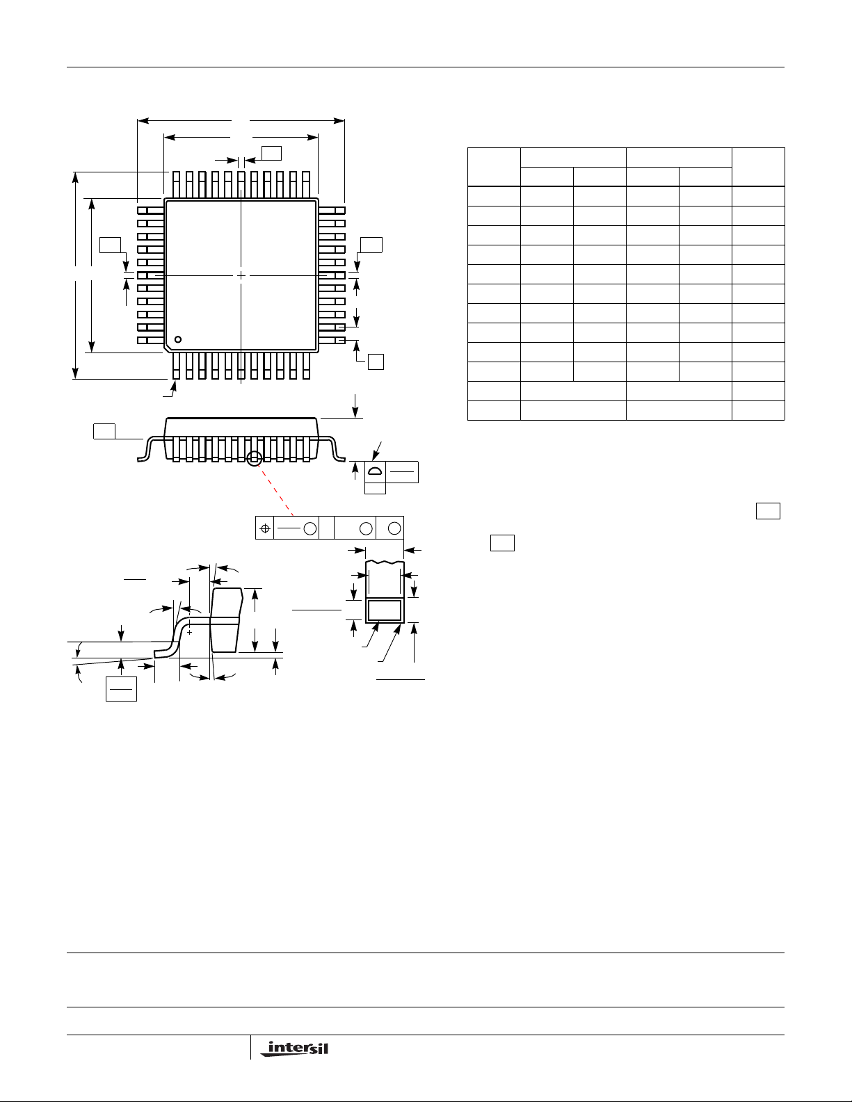
ISL6592
Thin Plastic Quad Flatpack Packages (LQFP)
E
E1
GAGE
PLANE
0o-7
D
D1
-D-
Q48.7x7A (JEDEC MS-026BBC ISSUE B)
48 LEAD THIN PLASTIC QUAD FLATPACK PACKAGE
INCHES MILLIMETERS
SYMBOL
NOTESMIN MAX MIN MAX
A - 0.062 - 1.60 A1 0.002 0.005 0.05 0.15 A2 0.054 0.057 1.35 1.45 -
-A-
-B-
b 0.007 0.010 0.17 0.2 7 6
b1 0.007 0.009 0.17 0.23 -
D 0.350 0.358 8.90 9.10 3
D1 0.272 0.280 6.90 7.10 4, 5
E 0.350 0.358 8.90 9.10 3
e
PIN 1
E1 0.272 0.280 6.90 7.10 4, 5
L 0.018 0.029 0.45 0.75 -
N48 487
e 0.020 BSC 0.50 BSC -
-H-
0.020
0.008
0o MIN
MIN
11o-13
A2
o
A1
0.08
0.003
0.09/0.16
0.004/0.006
SEATING
PLANE
A
0.08
0.003
-C-
NOTES:
1. Controlling dimension: MILLIMETER. Converted inch
dimensions are not necessarily exact.
2. All dimensions and tolerances per ANSI Y14.5M-1982.
3. Dimensions D and E to be determined at seating plane .
C
M
S
S
b
b1
4. Dimensions D1 and E1 to be determined at datum plane
-H-
.
5. Dimensions D1 and E1 do not include mold protrusion.
Allowable protrusion is 0.25mm (0.010 inch) per side.
D
A-B
6. Dimension b does not include dambar protrusion. Allowable
dambar protrusion shall not cause the lead width to exceed
the maximum b dimension by more than 0.08mm (0.003
Rev. 2 1/99
-C-
inch).
BASE METAL
L
0.25
o
0.010
11o-13
o
WITH PLATING
0.09/0.20
0.004/0.008
7. “N” is the number of terminal positions.
All Intersil U.S. products are manufactured, assembled and tested utilizing ISO9000 quality systems.
Intersil Corporation’s quality certifications can be viewed at www.intersil.com/design/quality
Intersil products are sold by description only. Intersil Corporation reserves the right to make changes in circuit design, software and/or specifications at any time without
notice. Accordingly, the reader is cautioned to verify that data sheets are current before placing orders. Information furnished by Intersil is believed to be accurate and
reliable. However, no responsibility is assumed by Intersil or its subsidiaries for its use; nor for any infringements of patents or other rights of third parties which may result
from its use. No license is granted by implication or otherwise under any patent or patent rights of Intersil or its subsidiaries.
For information regarding Intersil Corporation and its products, see www.intersil.com
21
FN9163.1
August 5, 2005
 Loading...