

Page 1
®
ISL6559
Data Sheet December 29, 2004
Multi-Phase PWM Controller
The ISL6559 provides core-voltage regulation by driving 2 to
4 interleaved synchronous-rectified buck-conv erter channels
in parallel. Interleaving the channel timing results in
increased ripple frequency which reduces input and output
ripple currents. The reduction in ripple results in lower
component cost, reduced dissipation, and a smaller
implementation area.
The ISL6559 uses cost and space-saving r
for channel current balance, active voltage positioning, and
over-current protection. Output voltage is monitored by an
internal differential remote sense amplifier. A high-bandwidth
error amplifier drives the output voltage to match the
programmed 5-bit DAC reference voltage. The resulting
compensation signal guides the creation of pulse width
modulated (PWM) signals to control companion Intersil
MOSFET drivers. The OFS pin allows direct offset of the
DAC voltage from 0V to 50mV using a single external
resistor. The entire system is trimmed to ensure a system
accuracy of ±
1% over temperature.
Outstanding features of this controller IC include
Dynamic VID
TM
technology allowing seamless on-the-fly VID
changing without the need of any external components.
Output voltage “droop” or active voltage positioning is
optional. When employed, it allows the reduction in size and
cost of the output capacitors required to support load
transients. A threshold-sensitive enable input allows the use
of an external resistor divider for start-up coordination with
Intersil MOSFET drivers or any other devices powered from
a separate supply.
Superior over-voltage protection is achiev ed by gating on the
lower MOSFET of all phases to crowbar the output voltage.
An optional second crowbar on V
, formed with an external
IN
MOSFET or SCR gated by the OVP pin, is triggered when
an over-voltage condition is detected. Under-voltage
conditions are detected, but PWM operation is not disrupted.
Over-current conditions cause a hiccup-mode response as
the controller repeatedly tries to restart. After a set number
of failed startup attempts, the controller latches off. A power
good logic signal indicates when the converter output is
between the UV and OV thresholds.
DS(ON)
sensing
FN9084.8
Features
• Multi-Phase Power Conversion
- 2, 3 or 4 Phase Operation
• Active Channel Current Balancing
• Precision r
Current Sharing
DS(ON)
- Lossless
-Low Cost
• Input Voltage: 12V or 5V Bias
• Precision CORE Voltage Regulation
-±
1% S y s t e m A c c u r a c y Over Temperature
- Differential Remote Output Voltage Sensing
- Programmable Reference Offset
• Microprocessor Voltage Identification Input
- 5-Bit VID Input
- 0.800V to 1.550V in 25mV Steps
- Dynamic VID Technology
• Programmable Droop Voltage
• Fast Transient Recovery Time
• Over Current Protection
• Digital Soft Start
• Threshold Sensitive Enable Input
• High Ripple Frequency (160kHz to 4MHz)
• QFN Package:
- Compliant to JEDEC PUB95 MO-220 QFN - Quad Flat
No Leads - Pac kage Outline
- Near Chip Scale Package f ootprint, which impro v es PC B
efficiency and has a thinner profile
• Pb-Free Available (RoHS Compliant)
Applications
• AMD Hammer F am ily Processor V ol t ag e Regu l a to r
• Low Output Vo ltage, High Current DC-DC Converters
• Voltage Regulator Modules
Pinouts
ISL6559CB (28 LEAD SOIC)
TOP VIEW TOP VIEW
28
27
26
25
24
23
22
21
20
19
18
17
16
15
EN
FS/DIS
PGOOD
PWM4
ISEN4
ISEN1
PWM1
PWM2
GND
ISEN2
ISEN3
PWM3
VCC
GND
GND
OVP
VID4
VID3
VID2
VID1
VID0
OFS
COMP
FB
IOUT
VDIFF
VSEN
RGND
1
2
3
4
5
6
7
8
9
10
11
12
13
14
ISL6559CR (32 LEAD QFN)
VID3NCVID4
32 31 30 29 28 27 26 25
VID2
1
VID1
2
VID0
3
NC
4
OFS
5
6
COMP
FB
7
NC
8
910111213141516
IOUT
VSEN
VDIFF
NC = NO CONNECT
OVP
GNDENFS/DIS
GND
RGND
GND
VCC
PGOOD
24
PWM4
23
ISEN4
22
ISEN1
21
PWM1
20
PWM2
19
GND
18
ISEN2
17
ISEN3
PWM3
1
Dynamic VID is a trademark of Intersil Americas Inc. All other trademarks mentioned are the property of their respective owners.
CAUTION: These devices are sensitive to electrostatic discharge; follow proper IC Handling Procedures.
1-888-INTERSIL or 321-724-7143
| Intersil (and design) is a registered trademark of Intersil Americas Inc.
Copyright © Intersil Americas Inc. 2002-2004. All Rights Reserved.
Page 2
ISL6559
Ordering Information
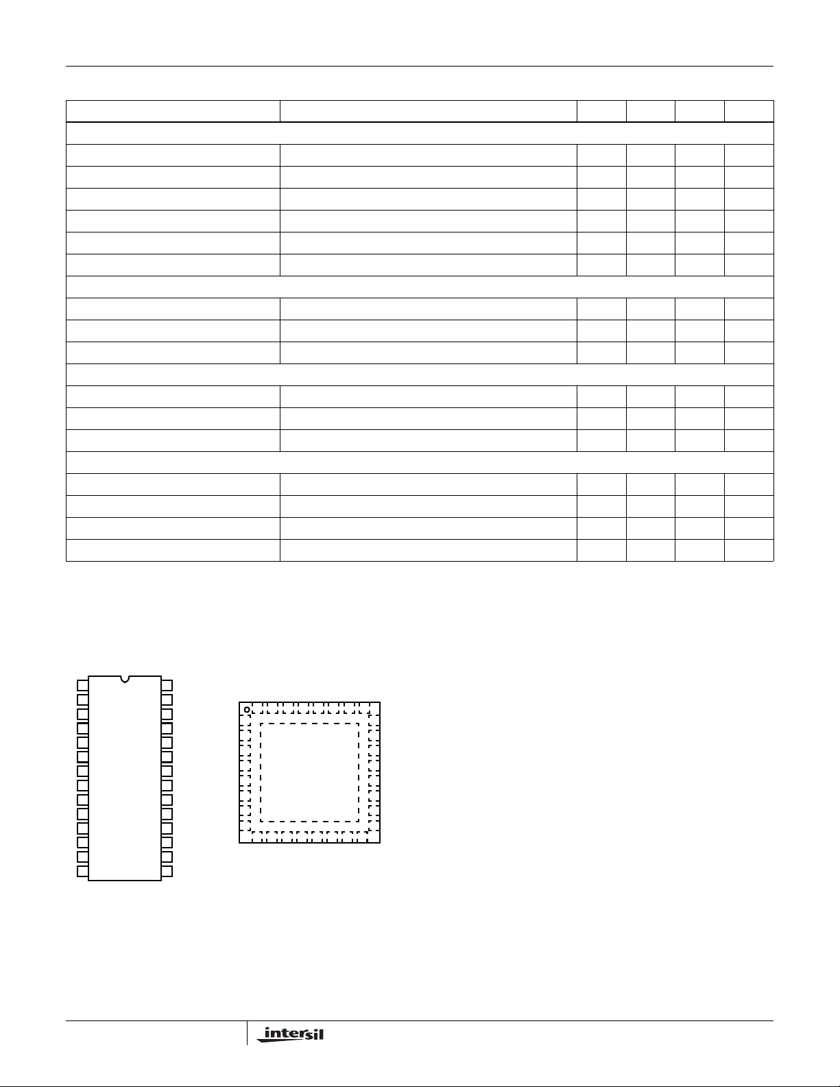
PART # TEMP. (°C) PACKAGE PKG. DWG. #
ISL6559CB 0 to 70 28 Ld SOIC M28.3
ISL6559CBZ* 0 to 70 28 Ld SOIC (Pb-free) M28.3
ISL6559CB-T 28 Ld SOIC Tape and Reel
ISL6559CBZ-T* 28 Ld SOIC Tape and Reel (Pb-free)
ISL6559CR 0 to 70 32 Ld 5x5 QFN L32.5x5
ISL6559CRZ* 0 to 70 32 Ld 5x5 QFN (Pb-free) L32.5x5
Block Diagram
PGOOD VCC
VID4
VID3
VID2
VID1
VID0
FB
COMP
OFS
DYNAMIC
VID
DAC
x 0.1
E/A
UV
-
+
350mV
POR
AND
SOFT START
+
+
+
Ordering Information (Continued)
PART # TEMP. (°C ) PACKAGE PKG. DW G. #
ISL6559CR-T 32 Ld 5x5 QFN Tape and Reel
ISL6559CRZ-T* 32 Ld 5x5 QFN Tape and Reel (Pb-free)
NOTE: * Intersil Pb-free products employ special Pb-free material sets;
molding compounds/die attach materials and 100% matte tin plate
termination finish, which are RoHS compliant and compatible with both
SnPb and Pb-free soldering operations. Intersil Pb-free products are
MSL classified at Pb-free peak reflow temperatures that meet or
exceed the Pb-free requirements of IPC/JEDEC J STD-020.
EN
1.23V
6V
-
+
+
-
+
+
FS/DIS
OSCILLATOR
AND
SAWTOOTH
PWM1
PWM2
PWM3
PWM4
VDIFF
VSEN
RGND
IOUT
100µA
DIFF
AVERAGE
2
2.2V
OV
90µA
OC
1/N
GND
-
+
OVP
I1
+
+
+
+
I2
I3
I4
N PHASES
CURRENT
SENSE
&
PHASE
DETECT
ISEN1
ISEN2
ISEN3
ISEN4
FN9084.8
December 29, 2004
Page 3
Typical Application - 3 Phase Converter
ISL6559
+12V
PVCC
+12V
BOOT
UGATE
VCC
DRIVER
HIP6601B
PWM
+12V
300Ω
ISL6559
VSEN
RGND
R
FB
C
C
R
C
R
OFS
R
T
VDIFF
FB
IOUT
COMP
OFS
FS/DIS
VID4
VID3
VID2
VID1
VID0
PGOOD
OVP
GND
VCC
PWM4
ISEN4
PWM1
ISEN1
PWM2
ISEN2
PWM3
ISEN3
NC
VCC
PWM
VCC
PWM
PVCC
PVCC
+12V
DRIVER
HIP6601B
+12V
DRIVER
HIP6601B
BOOT
BOOT
PHASE
LGATE
GND
UGATE
PHASE
LGATE
GND
UGATE
PHASE
LGATE
GND
+12V
+12V
R
R
R
ISEN1
ISEN2
ISEN3
V
OUT
3
FN9084.8
December 29, 2004
Page 4
ISL6559
Absolute Maximum Ratings
Supply Voltage, VCC . . . . . . . . . . . . . . . . . . . . . . . . . . . . . . . . . +7V
Input, Output, or I/O Voltage. . . . . . . . . . .GND -0.3V to V
ESD Classification . . . . . . . . . . . . . . . . . . . . . . . . . . . . . .Class TBD
CC
+ 0.3V
Thermal Information
Thermal Resistance θJA (°C/W) θJC (°C/W)
SOIC Package (Note 1) . . . . . . . . . . . . 60 N/A
QFN Package (Note 2). . . . . . . . . . . . . 33 4
Maximum Junction Temperature . . . . . . . . . . . . . . . . . . . . . . . 150°C
Operating Conditions
Supply Voltage, VCC . . . . . . . . . . . . . . . . . . . . . . . . . . . . . +5V ±5%
Ambient Temperature . . . . . . . . . . . . . . . . . . . . . . . . . . . 0°C to 70°C
Maximum Storage Temperature Range. . . . . . . . . . . -65°C to 150°C
Maximum Lead Temperature (Soldering 10s) . . . . . . . . . . . . . 300°C
(SOIC - Lead Tips Only)
Junction Temperature . . . . . . . . . . . . . . . . . . . . . . . . . .0°C to 125°C
CAUTION: Stress above those listed in “Absolute Maximum Ratings” may cause permanent damage to the de vice. This is a stress only rating and operation of the device
at these or any other conditions above those indicated in the operational section of this specification is not implied.
NOTES:
is measured with the component mounted on a high effective thermal conductivity test board in free air. See Tech Brief TB379 for details.
1. θ
JA
2. θ
is measured in free air with the component mounted on a high effective thermal conductivity test board with “direct attach” features. θ
JA
JC,
the
“case temp” is measured at the center of the exposed metal pad on the package underside. See Tech Brief TB379.
Electrical Specifications Operating Conditions: VCC = 5V, T
= 0°C to 70°C. Unless Otherwise Specified.
A
PARAMETER TEST CONDITIONS MIN TYP MAX UNITS
VCC SUPPLY CURRENT
Nominal Supply VCC = 5VDC; EN = 5VDC; R
Shutdown Supply VCC = 5VDC; EN = 0VDC; R
= 100 kΩ ±1% 8.0 10.8 14.0 mA
T
= 100 kΩ ±1% 8.0 10.3 13.0 mA
T
SHUNT REGULATOR
VCC Voltage VCC tied to 12VDC thru 300Ω resistor, R
VCC Sink Current VCC tied to 12VDC thru 300Ω resistor, R
= 100kΩ 5.63 5.8 5.97 V
T
= 100kΩ 15 20 25 mA
T
POWER-ON RESET AND ENABLE
POR Threshold VCC Rising 4.25 4.35 4.50 V
VCC Falling 3.75 3.85 4.00 V
ENABLE Threshold EN Rising 1.205 1.23 1.255 V
Hysteresis 86 92 98 mV
REFERENCE VOLTAGE AND DAC
Reference Voltage 0.792 0.8 0.808 V
System Accuracy (Note 3) -1 - 1 %VID
VID on Fly Step Size R
= 100kΩ -25-mV
T
VID Pull Up --20-µA
VID Input Low Level --1V
VID Input High Level - 1.36 1.60 V
PIN-ADJUSTABLE OFFSET
OFS Current -100- µA
Offset Accuracy ROFS = 5.00kΩ ±1% 47.0 50.0 53.0 mV
OSCILLATOR
Accuracy -10 - 10 %
Adjustment Range 0.08 - 1.0 MHz
Disable Voltage I
= 1mA 0.8 1.0 1.2 V
FS/DIS
Sawtooth Amplitude -1.37- V
Max Duty Cycle -75-%
4
FN9084.8
December 29, 2004
Page 5
ISL6559
Electrical Specifications Operating Conditions: VCC = 5V, T
= 0°C to 70°C. Unless Otherwise Specified. (Continued)
A
PARAMETER TEST CONDITIONS MIN TYP MAX UNITS
ERROR AMPLIFIER
Open-Loop Gain R
Open-Loop Bandwidth C
Slew Rate C
Maximum Output Voltage R
= 10kΩ to ground - 72 - dB
L
= 100pF, RL = 10kΩ to ground - 18 - MHz
L
= 100pF, Load = ±400mA - 7.1 11 V/µs
L
= 10kΩ to ground 3.6 4.5 - V
L
Source Current 3.0 7.0 9.5 mA
Sink Current 1.6 3.0 5.4 mA
REMOTE-SENSE AMPLIFIER
Input Impedance -80-kΩ
Bandwidth -20-MHz
Slew Rate -6-V/µs
SENSE CURRENT
IOUT Accuracy ISEN1 = ISEN2 = ISEN3 = ISEN4 = 50µA -5 - 5 %
ISEN Offset Voltage -6-mV
Over-Current Trip Level 72 90 108 µA
POWER GOOD AND PROTECTION MONITORS
PGOOD Low Voltage I
= 4mA - - 0.4 V
PGOOD
Under-Voltage Offset From VID VSEN Falling 320 350 420 mV
Over-Voltage Threshold VSEN Rising 2.08 2.13 2.20 V
OVP Voltage I
= 100mA, VCC = 5V 2.2 3.28 4.0 V
OVP
NOTE:
3. These parts are designed and adjusted for accuracy within the system tolerance
Functional Pin Description
VID2
VID1
VID0
NC
OFS
COMP
FB
NC
ISL6559CR (32 LEAD QFN)ISL6559CB (28 LEAD SOIC)
TOP VIEW
VID3NCVID4
32 31 30 29 28 27 26 25
1
2
3
4
5
6
7
8
9 10111213141516
IOUT
NC = NO CONNECT
OVP
GNDENFS/DIS
GND
VSEN
VDIFF
RGND
GND
VCC
TOP VIEW
28
27
26
25
24
23
22
21
20
19
18
17
16
15
EN
FS/DIS
PGOOD
PWM4
ISEN4
ISEN1
PWM1
PWM2
GND
ISEN2
ISEN3
PWM3
VCC
GND
GND
OVP
VID4
VID3
VID2
VID1
VID0
OFS
COMP
FB
IOUT
VDIFF
VSEN
RGND
1
2
3
4
5
6
7
8
9
10
11
12
13
14
GND
Bias and reference ground for the IC.
OVP
Over-voltage protection pin. This pin pulls to VCC and is
latched when an over-voltage condition is detected. Connect
PGOOD
PWM4
24
ISEN4
23
ISEN1
22
PWM1
21
PWM2
20
GND
19
ISEN2
18
ISEN3
17
PWM3
this pin to the gate of an SCR or MOSFET tied across V
IN
and ground to prevent damage to a load device.
VID4, VID3, VID2, VID1, VID0
The state of these five inputs program the internal DAC,
which provides the reference voltage for output regulation.
Connect these pins to either open-drain or active pull-up
type outputs. Pulling these pins above 2.9V can cause a
reference offset inaccuracy.
OFS
Connecting a resistor between this pin and ground creates a
positive offset voltage which is added to the DAC voltage,
allowing easy implementation of load-line regulation. For no
offset, simply tie this pin to ground.
FB and COMP
The internal error amplifier inverting input and output
respectively. Connect the external R-C feedback
compensation network of the regulator to these pins.
IOUT
The current carried out of this pin is proportional to output
current and can be used to incorporate output voltage droop
5
FN9084.8
December 29, 2004
Page 6
ISL6559
and/or load sharing. The scale f actor is set b y the r atio of th e
ISEN resistors and the lower MOSFET r
DS(ON)
. If droop is
desired, connect this pin to FB. When not used for droop or
load sharing, simply leave this pin open.
VSEN, RGND, VDIFF
VSEN and RGND are the inputs to the differential remotesense amplifier. Connect these pins to the sense points of
the remote load. Connect an appropriately sized feedback
resistor, R
, between VDIFF and FB.
FB
VCC
Supplies all the power necessary to operate the chip. The IC
starts to operate when the voltage on this pin exceeds the
rising POR threshold and shuts down when the voltage on
this pin drops below the falling POR threshold. Connect this
pin directly to a +5V supply or through a series 300Ω resistor
to a +12V supply.
ISEN1, ISEN2, ISEN3, ISEN4
Current sense inputs. A resistor connected between these
pins and their respective phase node sets a current
proportional to the current in the lower MOSFET during it’s
conduction interval. This current is used as a reference for
channel balancing, load sharing, protection, and load-line
regulation. Inactive channels should have their respective
sense inputs left open.
PWM1, PWM2, PWM3, PWM4
Pulse-width modulating outputs. Connect these pins to the
individual HIP660x driver PWM input pins. These logic
outputs command the driver IC(s) in switching the halfbridge configuration of MOSFETs.The number of active
channels is determined by the state of PWM3 and PWM4. If
PWM3 is tied to VCC, this indicates to the controller that two
channel operation is desired. In this case, PWM 4 should be
left open or tied to VCC. Shorting PWM4 to VCC indicates
that three channel operation is desired.
PGOOD
Power good is an open-drain logic output that changes to a
logic low when the voltage at VDIFF is 350mV below the VID
setting or above 2.2V.
FS/DIS
A dual function pin for setting the switching frequency and
disabling the controller. Place a resistor from this pin to
ground to set the switching frequency between 80kHz and
1MHz. Pulling this pin below 0.8V disables the controller.
EN
Threshold sensitive enable input of the controller. Transition
this pin above 1.23V (typical enable threshold) to initiate a
soft-start cycle. Pull this pin below 1.14V , taking into account
the enable hysteresis, to disable the controller once in
operation. Connect a resistor divider to this pin to set the
power-on voltage level for proper coordination with Intersil
MOSFET drivers. If this function is not required, simply tie
this pin to VCC.
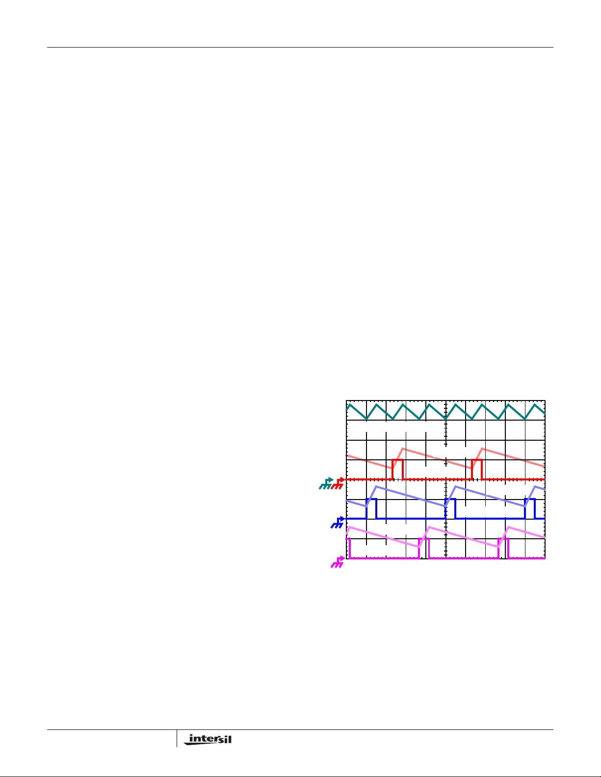
Multi-Phase Power Conversi on
Microprocessor load current profiles have changed to the
point where the multi-phase power conversion advantage is
pronounced. The technical challenges associated with
producing a single-phase converter which is both costeffective and thermally viable have forced a change to the
cost-saving approach of multi-phase. The ISL6559 controller
helps reduce the complexity of implementation by integrating
vital functions and requiring minimal output components.
The block diagram in Figure 1 provides a top level view of
multi-phase power conversion using the ISL6559 controller.
Interleaving
The switching of each channel in a multi-phase converter is
timed to be symmetrically out of phase with each of the other
channels. In a 3-phase converter, each channel switches 1/3
cycle after the previous channel and 1/3 cycle before the
following channel. As a result, the three-phase converter has
a combined ripple frequency three times greater than the
ripple frequency of any one phase. In addition, the peak-topeak amplitude of the combined inductor currents is reduced
in proportion to the number of phases (Equations 1 and 2).
Increased ripple frequency and lower ripple amplitude mean
that the designer can use less per-channel inductance and
lower total output capacitance for any performance
specification.
IL1 + IL2 + IL3, 7A/DIV
IL3, 7A/DIV
PWM3, 5V/DIV
IL2, 7A/DIV
PWM2, 5V/DIV
IL1, 7A/DIV
PWM1, 5V/DIV
1µs/DIV
FIGURE 1. PWM AND INDUCTOR-CURRENT WA VEFORMS
FOR 3-PHASE CONVERTER
Figure 1 illustrates the multiplicative effect on output ripple
frequency. The three channel currents (IL1, IL2, and IL3),
combine to form the AC ripple current and the DC load
current. The ripple component has three times the ripple
frequency of each individual channel current. Each PWM
pulse is terminated 1/3 of a cycle, or 1.33µs, after the PWM
pulse of the previous phase. The peak-to-peak current
waveforms for each phase is about 7A, and the dc
components of the inductor currents combine to feed the load.
6
FN9084.8
December 29, 2004
Page 7
ISL6559
To understand the reduction of ripple current amplitude in
the multi-phase circuit, examine the equation representing
an individual channel’s peak-to-peak inductor current.
VINV
–()V
OUT
I
------------------------------------------------------=
PP
LfSV
In Equation 1, V
IN
and V
IN
OUT
are the input and output
OUT
(EQ. 1)
voltages respectively, L is the single-channel inductor value,
and f
is the switching frequency.
S
The output capacitors conduct the ripple component of the
inductor current. In the case of multi-phase converters, the
capacitor current is the sum of the ripple currents from each
of the individual channels. Compare Equation 1 to the
expression for the peak-to-peak current after the summation
of N symmetrically phase-shifted inductor currents in
Equation 2. Peak-to-peak ripple current decreases by an
amount proportional to the number of channels. Outputvoltage ripple is a function of capacitance, capacitor
equivalent series resistance (ESR), and inductor ripple
current. Reducing the inductor ripple current allows the
designer to use fewer or less costly output capacitors.
VINNV
–()V
OUT
I
------------------------------------------------------------=
CPP,
LfSV
OUT
IN
(EQ. 2)
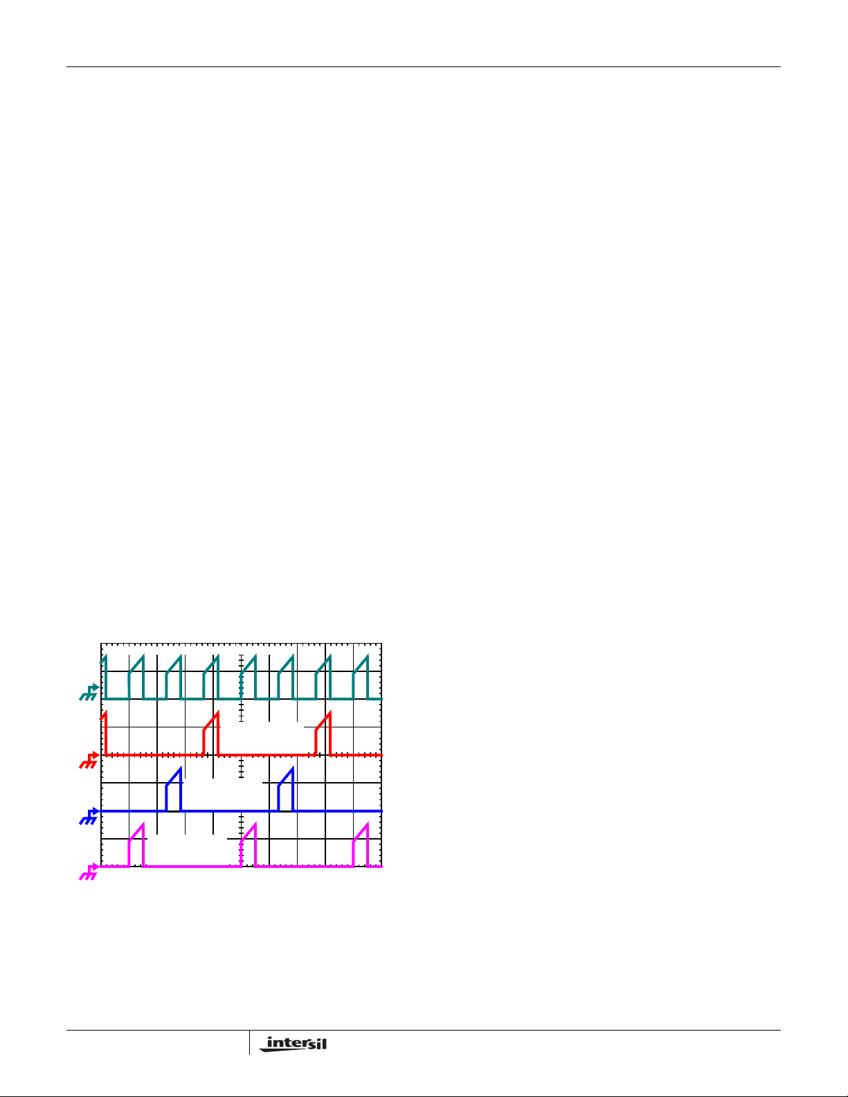
Another benefit of interleaving is to reduce input ripple
current. Input capacitance is determined in part by the
maximum input ripple current. Multi-phase topologies can
improve overall system cost and size b y lowe ring input ripple
current and allowing the designer to reduce the cost of input
capacitance. The example in Figure 2 illustrates input
currents from a three-phase converter combining to reduce
the total input ripple current.
INPUT-CAPACITOR CURRENT, 10A/DIV
CHANNEL 3
INPUT CURRENT
10A/DIV
CHANNEL 2
INPUT CURRENT
10A/DIV
CHANNEL 1
INPUT CURRENT
10A/DIV
1µs/DIV
FIGURE 2. CHANNEL INPUT CURRENTS AND INPUT-
CAPACITOR RMS CURRENT FOR 3-PHASE
CONVERTER
The converter depicted in Figure 2 delivers 36A to a 1.5V
load from a 12V input. The RMS input capacitor current is
5.9A. Compare this to a single-phase converter also
stepping down 12V to 1.5V at 36A. The single-phase
converter has 11.9A RMS input capacitor current. The
single-phase converter must use an input capacitor bank
with twice the RMS current capacity as the equivalent threephase converter.
Figures 15, 16 and 17 in the section entitled Input Capacitor
Selection can be used to determine the input-capacitor RMS
current based on load current, duty cycle, and the number of
channels. They are provided as aids in determining the
optimal input capacitor solution. Figure 18 shows the single
phase input-capacitor RMS current for comparison.
PWM Operation
The timing of each converter leg is set by the number of
active channels. The default channel setting for the ISL6559
is four. One switching cycle is defined as the time between
PWM1 pulse termination signals. The pulse termination
signal is an internally generated clock signal which triggers
the falling edge of PWM1. The cycle time of the pulse
termination signal is the inverse of the switching frequency
set by the resistor between the FS/DIS pin and ground. Each
cycle begins when the clock signal commands the channel-1
PWM output to go low. The PWM1 transition signals the
channel-1 MOSFET driver to turn off the channel-1 upper
MOSFET and turn on the channel-1 synchronous MOSFET.
In the default channel configuration, the PWM2 pulse
terminates 1/4 of a cycle after PWM1. The PWM 3 output
follows another 1/4 of a cycle after PWM2. PWM4 terminates
another 1/4 of a cycle after PWM3.
If PWM3 is connected to VCC, then two channel operation is
selected and the PWM2 pulse terminates 1/2 of a cycle later.
Connecting PWM4 to VCC selects three channel operation
and the pulse-termination times are spaced in 1/3 cycle
increments.
Once a PWM signal transitions low, it is held low for a
minimum of 1/4 cycle. This forced off time is required to
ensure an accurate current sample. Current sensing is
described in the next section. After the forced off time
expires, the PWM output is enabled. The PWM output state
is driven by the position of the error amplifier output signal,
V
, minus the current correction signal relative to the
COMP
sawtooth ramp as illustrated in Figure 1. When the modified
V
voltage crosses the sawtooth ramp, the PWM output
COMP
transitions high. The MOSFET driver detects the change in
state of the PWM signal and turns off the synchronous
MOSFET and turns on the upper MOSFET. The PWM signal
will remain high until the pulse termination signal marks the
beginning of the next cycle by triggering the PWM signal low.
Current Sensing
During the forced off time following a PWM transition low , the
controller senses channel load current by sampling the
voltage across the lower MOSFET r
ground-referenced amplifier, internal to the ISL6559,
connects to the PHASE node through a resistor, R
voltage across R
is equivalent to the voltage drop
ISEN
, see Figure 3. A
DS(ON)
ISEN
. The
7
FN9084.8
December 29, 2004
Page 8

ISL6559
V
IN
r
I
SEN
In
SAMPLE
&
HOLD
ISL6559 INTERNAL CIRCUIT EXTERNAL CIRCUIT
FIGURE 3. INTERNAL AND EXTERNAL CURRENT -SENSING
across the R
DS ON()
--------------------------=
I
L
R
ISEN
ISEN(n)
+
CIRCUITRY
of the lower MOSFET while it is
DS(ON)
R
CHANNEL N
LOWER MOSFET
ISEN
CHANNEL N
UPPER MOSFET
I
L
ILr
DS ON()
+
conducting. The resulting current into the ISEN pin is
proportional to the channel current, I
. The ISEN current is
L
then sampled and held after sufficient settling time every
switching cycle. The sampled current, I
, is used for channel-
n
current balance, load-line regulation, overcurrent protection,
and module current sharing. From Figure 3, the following
equation for I
InI
L
where I
If R
DS(ON)
is derived:
n
r
DS ON()
----------------------=
R
ISEN
is the channel current.
L
sensing is not desired, an independent current-
(EQ. 3)
sense resistor in series with the lower MOSFET source can
serve as a sense element. The circuitry shown in Figure 3
represents channel n of an N-channel converter. This
circuitry is repeated for each channel in the converter, but
may not be active depending upon the status of the PWM3
and PWM4 pins as described in the previous section.
Channel-Current Balance
The sampled current, In, from each active channel is used to
gauge both overall load current and the relative channel
current carried in each leg of the converter. The individual
sample currents are summed and divided by the number of
V
COMP
FIGURE 4. CHANNEL-1 PWM FUNCTION AND CURRENT-
+
-
f(jω)
I
ER
+
NOTE: *CHANNELS 3 and 4 are OPTIONAL.
BALANCE ADJUSTMENT
SAWTOOTH SIGNAL
I
AVG
-
I
1
÷ N
+
-
Σ
PWM1
I4 *
I
*
3
I
2
active channels. The resulting average current, I
AVG
,
provides a measure of the total load current demand on the
converter and the appropriate level of channel current. Using
Figures 3 and 4, the average current is defined as
I1I2…I
I
AVG
I
AVG
++
----------------------------------=
I
OUT
------------N
where N is the number of active channels and I
N
N
r
DS ON()
----------------------=
R
ISEN
OUT
(EQ. 4)
is the
total load current.
The average current is then subtracted from the individual
channel sample currents. The resulting error current, I
then filtered before it adjusts V
. The modified V
COMP
, is
ER
COMP
signal is compared to a sawtooth ramp signal and produces
a pulse width which corrects for any unbalance and drives
the error current toward zero. Figure 4 illustrates Intersil’s
patented current-balance method as implemented on
channel-1 of a multi-phase converter.
Two considerations designers face are MOSFET selection
and inductor design. Both are significantly improved when
channel currents track at any load level. The need for
complex drive schemes for multiple MOSFETs, exotic
magnetic materials, and expensive heat sinks is avoided.
Resulting in a cost-effective and easy to implement solution
relative to single-phase conversion. Channel-current balance
insures the thermal advantage of multi-phase conversion is
realized. Heat dissipation is spread over multiple channels
and a greater area than single phase approaches.
In some circumstances, it may be necessary to deliberately
design some channel-current unbalance into the system. In
a highly compact design, one or two channels may be able to
cool more effectively than the other(s) due to nearby air flow
or heat sinking components. The other channel(s) may have
more difficulty cooling with comparatively less air flow and
heat sinking. The hotter channels may also be located close
to other heat-generating components tending to drive their
temperature even higher. In these cases, the proper
selection of the current sense resistors (R
in Figure 3)
ISEN
introduces channel current unbalance into the system.
Increasing the value of R
in the cooler channels and
ISEN
decreasing it in the hotter channels moves all channels into
thermal balance at the expense of current balance.
Voltage Regulation
The output of the error amplifier , V
sawtooth waveform to modulate the pulse width of the PWM
signals. The PWM signals control the timing of the Intersil
MOSFET drivers and regulate the converter output to the
specified reference voltage. Three distinct inputs to the error
amplifier determine the voltage level of V
and external circuitry which control voltage regulation is
illustrated in Figure 5.
, is compared to the
COMP
. The internal
COMP
8
FN9084.8
December 29, 2004
Page 9

ISL6559
Most multi-phase controllers simply have the output voltage
fed back to the inv erting input of the error amplifier through a
resistor. The ISL6559 features an internal differential
remote-sense amplifier in the feedback path. The amplifier
removes the voltage error encountered when measuring the
output voltage relative to the local controller ground
reference point, resulting in a more accurate means of
sensing output voltage. Connect the microprocessor sense
pins to the non-inverting input, VSEN, and inverting input,
RGND, of the remote-sense amplifier. The remote-sense
amplifier output, V
, is then tied through an external
DIFF
resistor to the inverting input of the error amplifier.
A digital to analog converter (DAC) generates a reference
voltage based on the state of logic signals at pins VID4
through VID0. The DAC decodes the a 5-bit logic signal
(VID) into one of the discrete voltages shown in Table 1.
Each VID input offers a 20µA pull-up to an internal 2.5V
source for use with open-drain outputs. External pull-up
resistors or active-high output stages can augment the pullup current sources, but a slight accuracy error can occur if
they are pulled above 2.9V. The DAC-selected reference
voltage is connected to the non-inverting input of the error
amplifier.
The ISL6559 features a second non-inverting input to the
error amplifier which allows the user to directly offset the
DAC refe rence voltage in the positive direction only. The
offset voltage is created by an internal current source which
EXTERNAL CIRCUIT ISL6559 INTERNAL CIRCUIT
C
C
R
C
+
R
V
FB
DROOP
-
V
R
OUT
GND
OFS
REMOTE
SENSE
POINTS
FIGURE 5. OUTPUT-V OL TAGE AND LOAD-LINE
COMP
FB
IOUT
VDIFF
VSEN
RGND
OFS
+
V
OFS
-
REGULATION
ERROR AMPLIFIER
-
I
AVG
REFERENCE
VOLTAGE
+
+
+
-
DIFFERENTIAL
REMOTE-SENSE
AMPLIFIER
1/10
100µA
V
COMP
OFFSET
VOLTAGE
feeds out the OFS pin into a use r sel e cte d external resistor
to ground. The resulting voltage across the resistor, V
OFS
, is
internally divided down by ten to create the offset voltage.
This method of offsetting the DAC voltage is more accurate
than external methods of level-shifting the FB pin.
TABLE 1. VOLTAGE IDENTIFICATION CODES
VID4 VID3 VID2 VID1 VID0 DAC
0 0 0 0 0 1.550
0 0 0 0 1 1.525
0 0 0 1 0 1.500
0 0 0 1 1 1.475
0 0 1 0 0 1.450
0 0 1 0 1 1.425
0 0 1 1 0 1.400
0 0 1 1 1 1.375
0 1 0 0 0 1.350
0 1 0 0 1 1.325
0 1 0 1 0 1.300
0 1 0 1 1 1.275
0 1 1 0 0 1.250
0 1 1 0 1 1.225
0 1 1 1 0 1.200
0 1 1 1 1 1.175
1 0 0 0 0 1.150
1 0 0 0 1 1.125
1 0 0 1 0 1.100
1 0 0 1 1 1.075
1 0 1 0 0 1.050
1 0 1 0 1 1.025
1 0 1 1 0 1.000
1 0 1 1 1 0.975
1 1 0 0 0 0.950
1 1 0 0 1 0.925
1 1 0 1 0 0.900
1 1 0 1 1 0.875
1 1 1 0 0 0.850
1 1 1 0 1 0.825
1 1 1 1 0 0.800
1 1 1 1 1 Shutdown
The integrating compensation network shown in Figure 5
assures that the steady-state error in the output voltage is
limited to the error in the reference voltage (output of the
DAC) plus offset errors in the OFS current source, remotesense and error amplifiers. Intersil specifies the guaranteed
tolerance of the ISL6559 to include all variations in current
9
FN9084.8
December 29, 2004
Page 10

ISL6559
sources, amplifiers and the reference so that the output
voltage remains within the specified system tolerance of
±
1% over temperature.
LOAD-LINE REGULATION
Microprocessor load current demands change from near noload to full load often during operation. The resulting sizable
transient current slew rate causes an output voltage spike
since the converter is not able to respond fast enough to the
rapidly changing current demands. The magnitude of the
spike is dictated by the ESR and ESL of the output
capacitors selected. In order to drive the cost of the output
capacitor solution down, one commonly accepted approach
is active voltage positioning. By adding a well controlled
output impedance, the output voltage can effectively be le v el
shifted in a direction which works against the voltage spike.
The average current of all the active channels, I
AVG
, flows
out IOUT, see Figure 5. IOUT is connected to FB through a
load-line regulation resistor, R
across R
is proportional to the output current, effectively
FB
. The resulting voltage drop
FB
creating an output voltage droop with a steady-state value
defined as
V
DROOPIAVGRFB
In most cases, each channel uses the same R
sense current. A more complete expression for V
=
ISEN
(EQ. 5)
value to
DROOP
is
derived by combining equations 3 and 4.
V
DROOP
=
------------N
DS ON()
---------------------- R
R
ISEN
FB
(EQ. 6)
I
r
OUT
Droop is an optional feature of the ISL6559. If active voltage
positioning is not required, simply leave the IOUT pin open.
DYNAMIC VID
Next generation microprocessors can change VID inputs at
any time while the regulator is in operation. The power
management solution is required to monitor the DAC inputs
and respond to VID voltage transitions or ‘on-the-fly’ VID
changes, in a controlled manner. Supervising the safe output
voltage transition within the DAC range of the processor
without discontinuity or disruption.
The ISL6559 checks the five VID inputs at the beginning of
each channel-1 switching cycle. If the VID code has
changed, the controller waits one complete switching cycle
to validate the new code. If the VID code is stable for this
entire switching cycle, then the controller will begin ex ecuting
the output voltage change. The controller begins
incrementing the reference voltage by making 25mV steps
every two switching cycles until it reaches the ne w VID code.
The total time required for a VID change, t
on the switching frequency (f
), the size of the change
S
, is dependent
DV
(∆VID), and the time before the next switching cycle begins.
Since the ISL6559 recognizes VID-code changes only at the
beginning of switching cycles, up to one full cycle may pass
before a VID change registers. This is followed by a onecycle wait before the output voltage begins to change. The
one-cycle uncertainty in Equation 8 is due to the possibility
that the VID code change may occur up to one full cycle
before being recognized.
1
2VID∆
---- -
------------------
f
0.025
S
1–
The time required for a converter running with f
t
DV
1
2VID∆
≤<
---- -
------------------
f
0.025
S
(EQ. 8)
= 500kHz to
S
make a 1.2V to 1.4V reference-voltage change is between
30µs and 32µs as calculated using Equation 8. This example
is also illustrated in Figure 7.
REFERENCE OFFSET
Typical microprocessor tolerance windows are centered
around a nominal DAC set point. Implementing a load-line
would require offsetti ng th e ou tput voltage above this
nominal DAC set point. Centering the load-line within the
static specification window. The ISL6559 features an internal
100µA current source which feeds out the OFS pin. Placing
a resistor from OFS and ground allows the user to set the
amount of positive offset desired directly to the reference
voltage. The voltage developed across the OFS resistor,
R
, is divided down internally by a factor of 10 and directly
OFS
counters the DAC v oltage at the error amplifier non-inv erting
input. Select the resistor value based on the voltage offset
desired, V
R
OFS
, using Equation 6.
OFS
V
10⋅
OFS
---------------------------=
100µ A
(EQ. 7)
10
01110 00110
V
, 100mV/DIV
1.2V
1.2V
REF
V
, 100mV/DIV
OUT
FIGURE 6. DYNAMIC-VID WAVEFORMS FOR 500KHZ
ISL6559 BASED MULTI-PHASE BUCK
CONVERTER
VID, 5V/DIV
VID CHANGE OCCURS
ANYWHERE HERE
5µs/DIV
December 29, 2004
FN9084.8
Page 11

ISL6559
Operation Initialization
Before converter operation is initialized, proper conditions
must exist on the enable and disable inputs. Once these
conditions are met, the controller begins a soft-start interval.
Once the output voltage is within the proper window of
operation, the PGOOD output changes state to update an
external system monitor.
Enable and Disable
The PWM outputs are held in a high-impedance state to
assure the drivers remain off while in shutdown mode. Four
separate input conditions must be met before the ISL6559 is
released from shutdown mode.
First, the bias voltage applied at VCC must reach the internal
power-on reset (POR) circuit rising threshold. Once this
threshold is met, the EN input signal becomes the gate for
soft-start initialization. Hysteresis between the rising and
falling thresholds insures that once enabled, the ISL6559 will
not inadvertently turn off unless the bias voltage drops
substantially. See Electrical Specifications for specifics on
POR rising and falling thresholds.
EXTERNAL CIRCUITISL6559 INTERNAL CIRCUIT
+5V
+12V
10.7kΩ
1.40kΩ
POR
CIRCUIT
OV LATCH
SIGNAL
ENABLE
COMPARATOR
+
-
1.23V (± 2%)
VCC
EN
The 11111 VID code is reserved as a signal to the controller
that no load is present. The controller will enter shutdown
mode after receiving this code and will start up upon
receiving any other code. This code is not intended as a
means of enabling the controller when a load is present.
To enable the controller, VCC must be greater than the POR
threshold; the voltage on EN must be greater than 1.23V;
FS/DIS must not be grounded; and VID cannot be equal to
11111. Once these conditions are true, the controller
immediately initiates a soft-start sequence.
Soft-Start
The soft-start time, tSS, is determined by an 11-bit counter
that increments with every pulse of the phase clock. For
example, a converter switching at 250kHz per phase has a
soft-start time of
2048
T
------------ -8.3ms==
SS
f
SW
During the soft-start interval, the soft-start voltage, V
increases linearly from zero to 140% of the programmed
DAC voltage. At the same time a current source, I
decreasing from 160µA down to zero. These signals are
connected as shown in Figure 8 (I
may or may not be
OUT
connected to FB depending on the particular application).
EXTERNAL CIRCUIT ISL6559 INTERNAL CIRCUIT
C
C
R
C
R
FB
COMP
FB
IOUT
VDIFF
ERROR AMPLIFIER
-
+
I
RAMP
(EQ. 9)
RAMP
, is
RAMP
V
COMP
REFERENCE
VOLTAGE
,
FIGURE 7. POWER SEQUENCING USING THRESHOLD-
SENSITIVE ENABLE (EN) FUNCTION
Second, the ISL6559 features an enable input (EN) for
power sequencing between the controller bias voltage and
another voltage rail. The enable comparator holds the
ISL6559 in shutdown until the voltage at EN rises above
1.23V. The enable comparator has about 90mV of hysteresis
to prevent bounce. It is important that the driver ICs reach
their POR level before the ISL6559 becomes enabled. The
schematic in Figure 7 demonstrates sequencing the ISL6559
with the HIP660X family of Intersil MOSFET drivers which
require 12V bias.
Third, the frequency select\disable input (FS/DIS) will
shutdown the converter when pulled to ground. Under this
condition, the internal oscillator is disabled. The oscillator
resumes operation upon release of FS/DIS and a soft-start
sequence is initiated.
11
V
I
AVG
FIGURE 8. RAMP CURRENT AND VOLTAGE FOR
REGULATING SOFT-START SLOPE
AND DURATION
RAMP
IDEAL DIODES
The ideal diodes in Figure 8 assure that the controller tries to
regulate its output to the lower of either the ref e rence voltage
or V
(R
V
RAMP
. Since I
RAMP
x 160µA), the first PWM pulse will not be seen until
FB
is greater than the RFBI
creates an initial offset across RFB of
RAMP
offset. This produces a
RAMP
delay after the ISL6559 enables before the output voltage
starts moving. For example, if VID = 1.5V, R
= 1kΩ and TSS
FB
= 8.3ms, the delay time can be expressed using Equation 10.
FN9084.8
December 29, 2004
Page 12

1
ISL6559
T
t
DELAY
--------------------------------------------------- 560µ s==
1
Following the delay, the soft start ramps linearly until V
---------------------------------------- -+
R
FB
SS
()
1.4 VID
160 10
×
(EQ. 10)
–
6
RAMP
reaches VID. F or the system described above , this first linear
ramp will continue for approximately
AMP1
5.27ms=
1.4
DELAY
(EQ. 1
T
SS
t
–
---------- -
=
The final portion of the soft-start sequence is the time
remaining after V
reaches VID and before I
RAMP
RAMP
gets to
zero. This is also char acterized by a sli ght change in the slope
of the output voltage ramp which, f or the current example,
exists for a time of
t
RAMP2TSStRAMP1
– t
2.34ms=
–=
DELAY
(EQ. 12)
This behavior is seen in the example in Figure 9 of a converter
switching at 500kHz. For this converter , R
leading to T
and t
RAMP2
= 4.0ms, t
SS
= 1.17ms.
DELA Y
= 700ns, t
is set to 2.67kΩ
FB
= 2.23ms,
RAMP1
VOUT, 500mV/DIV
outlines the interaction between the f ault monito rs and the
power good signal.
PGOOD
UV
-
+
+
350mV
-
DAC
REFERENCE
VDIFF
FIGURE 10. POWER GOOD AND PROTECTION CIRCUITRY
2.2V
+
OV
-
POR
CIRCUIT
-
OC
+
90µA
I
AVG
OVP
Power Good Signal
The power good pin (PGOOD) is an open-drain logic output
which indicates that the converter is operating properly and
the output voltage is within a set window. The under-voltage
(UV) and over-voltage (OV) comparators create the output
voltage window. The controller also takes advantage of
current feedback to detect output over-current (OC)
conditions. PGOOD pulls low during shutdown and releases
high during soft-start once the output voltage exceeds the
UV threshold. Once high, PGOOD will only transition low
when the controller is disabled or a fault condition is
detected. It will return high under certain circumstances
once a fault clears.
EN, 5V/DIV
t
DELAYtRAMP1tRAMP2
FIGURE 9. SOFT-START WAVEFORMS FOR ISL6559 BASED
MULTI-PHASE BUCK CONVERTER
NOTE: Switching frequency 500kHz and RFB = 2.67kΩ
1ms/DIV
Fault Monitoring and Protection
The ISL6559 actively monitors voltage and current feedback
to detect fault conditions. Fault monitors trigger protective
measures to prevent damage to a microprocessor load. One
common power good indication signal is provided for linking
to external system monitors. The schematic in Figure 10
12
Under-Voltage Protection
The voltage on V
is compared with the DAC reference voltage. By positively
offsetting the output voltage, an UV threshold is created
which moves relative to the VID code. During soft-start, the
slow rising output voltage eventually exceeds the UV
threshold. Assuming the POR leg of the PGOOD NOR gate
has not detected an OC fault, the PGOOD signal will go
high.
If a fault condition arises during operation and the output
voltage drops below the UV threshold, PGOOD will
immediately pull low, but converter operation will continue.
PGOOD will return high once the output voltage surpasses
the UV threshold.
If the ISL6559 is disabled during operation, the PGOOD
signal will not pull low until the output voltage decays below
the UV threshold.
is internally offset by 350mV before it
DIFF
December 29, 2004
FN9084.8
Page 13

ISL6559
Over-Voltage Protection
When the output of the differential amplifier (VDIFF) reaches
2.2V, PGOOD immediately goes low indicating a fault. Two
protective actions are taken by the ISL6559 to protect the
microprocessor load.
First, all PWM outputs are commanded low. Directing the
Intersil drivers to turn on the lower MOSFETs; shunting the
output to ground preventing any further increase in output
voltage. The PWM outputs remain low until VDIFF falls to the
programmed DAC level at which time they go into a highimpedance state. The Intersil drivers respond by turning off
both upper and lower MOSFETs. If the over-voltage
condition reoccurs, the ISL6559 will again command the
lower MOSFETs to turn on. The ISL6559 will continue to
protect the load in this fashion as long as the over-voltage
repeats.
Second, the OVP pin pulls to VCC and can deliver 100mA
into the gate of either a MOSFET or SCR placed across the
input voltage (V
) and V
IN
. Turning on the MOSFET or
OUT
SCR collapses the power rail and causes a fuse placed
further up stream to blow. The fuse must be sized such that
the MOSFET or SCR will not overheat before the fuse blows .
Once an over-voltage condition is detected, normal PWM
operation ceases and PGOOD remains low until the
ISL6559 is reset. Cycling the voltage on EN below 1.23V or
the bias to VCC below the POR-falling threshold will reset
the controller.
Over-Current Protection
The ISL6559 takes advantage of the proportionality between
the load current and the average current, I
over-current condition. See the Channel-Current Balance
section for more detail on how the average current is
created. The average current is continually compared with a
constant 90µA reference current. Once the average current
exceeds the reference current, the comparator triggers the
converter to shutdown. The POR circuit places all PWM
signals in a high-impedance state which commands the
drivers to turn off both upper and lower MOSFETs. PGOOD
pulls low and the system remains in this state while the
, to detect an
AVG
controller counts 2048 phase clock cycles. This is followed
by a soft-start attempt (see Soft-Start).
OUTPUT CURRENT, 20A/DIV
0A
OUTPUT VOLTAGE,
500mV/DIV
0V
FIGURE 11. OVERCURRENT BEHAVIOR IN HICCUP MODE
5ms/DIV
During the soft-start interval, the over-current protection
circuitry remains active. As the output voltage ramps up, if an
over-current condition is detected, the ISL6559 immediately
places all PWM signals in a high-impedance state. The
ISL6559 repeats the 2048-cycle wait period and follows with
another soft-start attempt, as shown in
Figure 11. This hiccup mode of operation repeats up to
seven times. On the eighth soft-start attempt, the part
latches off. Once latched off, the ISL6559 can only be reset
when the voltage on EN is brought below 1.23V or VCC is
brought below the POR falling threshold. Upon completion of
a successful soft-start attempt, operation will continue as
normal, PGOOD will return high, and the OC latch counter is
reset.
During VID-on-the-fly transitions, the OC comparator output
is blanked. The quality and mix of output capacitors used in
different applications leads to a wide output capacitance
range. Depending upon the magnitude and direction of the
VID change, the change in voltage across the output
capacitors could result in significant current flow. Summing
this instantaneous current with the load current already
present could drive the average current above the reference
current level and cause an OC trip during the transition. By
blanking the OC comparator during the VID-on-the-fly
transition, nuisance tripping is avoided.
13
General Design Guide
This design guide is intended to provide a high-level
explanation of the steps necessary to create a multi-phase
power conv erter . It is assumed that the reader i s familiar with
many of the basic skills and techniques ref erenced b elo w. In
addition to this guide, Intersil provides complete reference
designs that include schematics, bills of materials, and
example board layouts for all common microprocessor
applications.
FN9084.8
December 29, 2004
Page 14

ISL6559
Power Stages
The first step in designing a multi-phase converter is to
determine the number of phases. This determination
depends heavily on the cost analysis which in turn depends
on system constraints that differ from one design to the ne xt.
Principally, the designer will be concerned with whether
components can be mounted on both sides of the circuit
board; whether through-hole components are permitted; and
the total board space available for power-supply circuitry.
Generally speaking, the most economical solutions are
those where each phase handles between 15 and 20A. All
surface-mount designs will tend toward the lower end of this
current range and, if through-hole MOSFETs can be used,
higher per-phase currents are possible. In cases where
board space is the limiting constraint, current can be pushed
as high as 30A per phase, but these designs require heat
sinks and forced air to cool the MOSFETs.
MOSFETS
The choice of MOSFETs depends on the current each
MOSFET will be required to conduct; the switching frequency;
the capability of the MOSFETs to dissipate heat; and the
availability and nature of heat sinking and air flo w.
LOWER MOSFET POWER CALCULATION
The calculation for heat dissipated in the lower MOSFET is
simple, since virtually all of the heat loss in the lower
MOSFET is due to current conducted through the channel
resistance (r
continuous output current; I
current (see Equation 1); d is the duty cycle (V
L is the per-channel inductance.
PLr
DS ON()
An additional term can be added to the lower-MOSFET loss
equation to account for additional loss accrued during the
dead time when inductor current is flowing through the
lower-MOSFET body diode. This term is dependent on the
diode forward voltage at I
f
; and the length of dead times, td1 and td2, at the
S
beginning and the end of the lower-MOSFET conduction
interval respectively.
P
=
DVDON()fS
Thus the total maximum power dissipated in each lower
MOSFET is approximated by the summation of P
UPPER MOSFET POWER CALCULATION
In addition to r
MOSFET losses are due to currents conducted across the
input voltage (V
higher portion of the upper-MOSFET losses are dependent
on switching frequency, the power calculation is more
). In Equation 13, IM is the maximum
DS(ON)
2
I
M
1d–()
----- N
I
I
M
----- -
-------- -+
N
losses, a large portion of the upper-
DS(ON)
) during switching. Since a subst an ti a l ly
IN
is the peak-to-peak inductor
PP
2
I
1d–()
LPP,
--------------------------------+=
12
PP
2
, V
M
t
d1
; the switching frequency ,
D(ON)
I
I
M
PP
+
----- N
t
–
-------- 2
d2
OUT/VIN
and PD.
L
); and
(EQ. 13)
(EQ. 14)
complex. Upper MOSFET losses can be divided into
separate components involving the upper-MOSFET
switching times; the lower-MOSFET body-diode reverserecovery charge, Q
; and the upper MOSFET r
rr
DS(ON)
conduction loss.
When the upper MOSFET turns off, the lower MOSFET does
not conduct any portion of the inductor current until the
voltage at the phase node falls below ground. Once the
lower MOSFET begins conducting, the current in the upper
MOSFET falls to zero as the current in the low er MOSFET
ramps up to assume the full inductor current. In Equation 15,
the required time for this commutation is t
approximated associated power loss is P
≈
P
UP 1,VIN
I
M
----- -
N
t
I
1
PP
-------- -+
2
----
2
f
S
and the
1
.
UP,1
(EQ. 15)
The upper MOSFET begins to conduct and this transition
occurs over a time t
loss is P
P
UP 2,VIN
.
UP,2
I
≈
----- -
. In Equation 16, the approximate power
2
t
I
M
N
2
PP
–
-------- 2
----
2
f
S
(EQ. 16)
A third component involves the lower MOSFET’s reverserecovery charge, Qrr. Since the inductor current has fully
commutated to the upper MOSFET before the lowerMOSFET’s body diode can draw all of Q
, it is conducted
rr
through the upper MOSFET across VIN. The power
dissipated as a result is P
P
UP 3,
VINQrrf
=
S
and is approximately
UP,3
(EQ. 17)
Finally, the resistive part of the upper MOSFET’s is given in
Equation 18 as P
P
UP 4,rDS ON()
In this case, of course, r
UP,4
2
I
M
----- N
.
+≈
d
DS(ON)
2
I
PP
---------12
is the on resistance of the
(EQ. 18)
upper MOSFET.
The total power dissipated by the upper MOSFET at full load
can now be approximated as the summation of the results
from Equations 15, 16, 17 and 18. Since the power
equations depend on MOSFET parameters, choosing the
correct MOSFETs can be an iterative process that involves
repetitively solving the loss equations for different MOSFETs
and different switching frequencies until converging upon the
best solution.
Current Sensing
The ISEN pins are denoted ISEN1, ISEN2, ISEN3 and
ISEN4. The resistors connected between these pins and
their respective phase nodes determine the gains in the
load-line regulation loop and the channel-current balance
14
FN9084.8
December 29, 2004
Page 15

ISL6559
loop. Select the values for these resistors based on the room
temperature r
operating current, I
of the lower MOSFETs; the full-load
DS(ON)
; and the number of phases, N
FL
according to Equation 19 (see also Figure 3).
R
ISEN
r
DS ON()
----------------------50 10
I
FL
------- -=
–
6
N
×
(EQ. 19)
In certain circumstances, it may be necessary to adjust the
value of one or more of the ISEN resistors. This can arise
when the components of one or more channels are inhibited
from dissipating their heat so that the affected channel s run
hotter than desired (see the section entitled Channel-Current
Balance). In these cases, chose new , smaller v alues of R
for the aff ected phases. Choose R
in proportion to the
ISEN,2
ISEN
desired decrease in temperature rise in order to cause
proportionally less current to flow in the hotter phase.
∆T
----------=
∆T
2
1
is the desired temperature
2
R
ISEN 2,
R
ISEN
In Equation 20, make sure that ∆T
rise above the ambient temperature , and ∆T
is the measured
1
(EQ. 20)
temperature rise above the ambient temperature. Whi le a
single adjustment according to Equation 20 is usually
sufficient, it may occasionally be necessary to adjust R
ISEN
two or more times to achiev e perfect thermal balance between
all channels.
COMPENSATING LOAD-LINE REGULATED
CONVERTER
The load-line regulated converter behaves in a similar
manner to a peak-current mode controller because the two
poles at the output-filter L-C resonant frequency split with
the introduction of current information into the control loop.
The final location of these poles is determined by the system
function, the gain of the current signal, and the value of the
compensation components, R
and CC.
C
Since the system poles and zero are effected by the values
of the components that are meant to compensate them, the
solution to the system equation becomes fairly complicated.
Fortunately there is a simple approximation that comes very
close to an optimal solution. Treating the system as though it
were a voltage-mode regulator by compensating the L-C
poles and the ESR zero of the voltage-mode approximation
yields a solution that is always stable with very close to ideal
transient performance.
C2 (OPTIONAL)
C
R
C
C
COMP
Load-Line Regulation Resistor
The load-line regulation resistor is labeled RFB in Figure 5.
Its value depends on the desired full-load droop voltage
(V
DROOP
in Figure 5). If Equation 19 is used to select each
ISEN resistor, the load-line regulation resistor is as shown
in Equation 21.
V
FB
DROOP
------------------------ -=
50 106–×
(EQ. 21)
R
If one or more of the ISEN resistors was adjusted for thermal
balance, as in Equation 20, the load-line regulation resistor
should be selected according to Equation 22. Where I
the full-load operating current and R
∑
n
th
ISEN pin.
ISEN n()
resistor connected to the n
V
R
FB
DROOP
-------------------------------- R
=
IFLr
DS ON()
ISEN(n)
is the ISEN
is
FL
(EQ. 22)
Compensation
The two opposing goals of compensating the voltage
regulator are stability and speed. Depending on whether the
regulator employs the optional load-line regulation as
described in Load-Line Regulation, there are two distinct
methods for achieving these goals.
FB
+
R
FB
FIGURE 12. COMPENSATION CONFIGURA TION FOR
The feedback resistor, R
V
DROOP
-
LOAD-LINE REGULATED ISL6559 CIRCUIT
, has already been chosen as
FB
IOUT
ISL6559
VDIFF
outlined in Load-Line Regulation Resistor. Select a target
bandwidth for the compensated system, f
. The target
0
bandwidth must be large enough to assure adequate
transient performance, but smaller than 1/3 of the perchannel switching frequency. The values of the
compensation components depend on the relationships of f
to the L-C pole frequency and the ESR zero frequency. For
0
15
FN9084.8
December 29, 2004
Page 16

ISL6559
each of the three cases which follow, there is a separate set
of equations for the compensation components.
1
------------------- f
Case 1:
Case 2:
Case 3:
------------------2π LC
R
CRFB
C
C
f
0
R
C
>
2π LC
R
CRFB
C
C
1
CRFB
C
0
2π f0VppLC
----------------------------------- -=
0.75V
------------------------------------=
2π VPPRFBf
f
0
VPP2π()2f
--------------------------------------------=
-------------------------------------------------------------=
2π()2f
0
1
------------------------------>
2π C ESR()
------------------------------------------=
0.75 V
0.75VINESR()C
-------------------------------------------------=
2π V
PPRFBf0
0.75V
IN
IN
0
1
------------------------------<≤
2π C ESR()
2
LC
0
0.75 V
IN
0.75V
IN
2
VPPRFBLC
2π f0VppL
ESR()
IN
L
(EQ. 23)
In Equations 23, L is the per-channel filter inductance
divided by the number of active channels; C is the sum total
of all output capacitors; ESR is the equivalent-series
resistance of the bulk output-filter capacitance; and V
PP
is
the peak-to-peak sawtooth signal amplitude as described in
Figure 4 and Electrical Specifications.
Once selected, the compensation values in Equations 23
assure a stable converter with reasonable transient
performance. In most cases, transient performance can be
improved by making adjustments to R
value of R
while observing the transient performance on an
C
. Slowly increase the
C
oscilloscope until no further improvement is noted. Normally,
C
will not need adjustment. Keep the value of CC from
C
Equations 23 unless some performance issue is noted.
The optional capacitor C
, is sometimes needed to bypass
2
noise away from the PWM comparator (see Figure 12). Keep
a position available for C
, and be prepared to install a high-
2
frequency capacitor of between 22pF and 150pF in case any
trailing edge jitter problem is noted.
C
2
C
C
R
C
C
1
R
R
1
FIGURE 13. COMPENSATION CIRCUIT FOR ISL6559 BASED
FB
CONVERTER WITHOUT LOAD-LINE
REGULATION.
COMP
FB
IOUT
ISL6559
VDIFF
COMPENSATION WITHOUT LOAD-LINE REGULATION
The non load-line regulated converter is accurately modeled
as a voltage-mode regulator with two poles at the L-C
resonant frequency and a zero at the ESR frequency. A
type III controller, as shown in Figure 13, provides the
necessary compensation.
The first step is to choose the desired bandwidth, f
, of the
0
compensated system. Choose a frequency high enough to
assure adequate transient performance but not higher than 1/3
of the switching frequency. The type-III compensator has an
extra high-frequency pole, f
. This pole can be used for added
HF
noise rejection or to assure adequate attenuation at the erroramplifier high-order pole and zero frequencies. A good general
rule is to chose f
Choosing f
HF
=10f0, but it can be higher if desired.
HF
to be lower than 10f0 can cause problems with
too much phase shift below the system bandwidth.
In the solutions to the compensation equations, there is a single
degree of freedom. For the solutions presented in Equations
24, R
is selected arbitrarily . The remaining compensation
FB
components are then selected according to Equations 24.
C ESR()
R1R
C
1
C
2
-----------------------------------------=
FB
LC C ESR()–
LC C ESR()–
-----------------------------------------=
R
FB
0.75V
------------------------------------------------------------------ -=
2π()2f0fHFLCRFBV
IN
PP
16
2
VPP2π
---------------------------------------------------------------------=
R
C
0.75V
0.75V
C
------------------------------------------------------------------ -=
C
2π()
f0fHFLCR
2π fHFLC 1–
IN
2π fHFLC 1–
IN
2
f0fHFLCRFBV
FB
PP
(EQ. 24)
FN9084.8
December 29, 2004
Page 17

ISL6559
In Equations 24, L is the per-channel filter inductance
divided by the number of active channels; C is the sum total
of all output capacitors; ESR is the equivalent-series
resistance of the bulk output-filter capacitance; and V
PP
is
the peak-to-peak sawtooth signal amplitude as described in
Figure 4 and Electrical Specifications.
Output Filter Design
The output inductors and the output capacitor bank together
form a low-pass filter responsible for smoothing the pulsating
voltage at the phase nodes. The output filter also must
provide the transient energy during the interval of time after
the beginning of the transient until the regulator can respond.
Because it has a low bandwidth compared to the switching
frequency, the output filter necessarily limits the system
transient response leaving the output capacitor bank to
supply or sink load current while the current in the output
inductors increases or decreases to meet the dema n d.
In high-speed converters, the output capacitor bank is
usually the most costly (and often the largest) part of the
circuit. Output filter design begins with minimizing the cost of
this part of the circuit. The critical load parameters in
choosing the output capacitors are the maximum size of the
load step, ∆I; the load-current slew rate, di/dt; and the
maximum allowable output-voltage de viation under transient
loading, ∆V
their capacitance, ESR, and ESL (equivalent series
inductance).
At the beginning of the load transient, the output capacitors
supply all of the transient current. The output voltage will
initially deviate by an amount approximated by the voltage
drop across the ESL. As the load current increases, the
voltage drop across the ESR increases linearly until the load
current reaches its final value. The capacitors selected must
have sufficiently low ESL and ESR so that the total outputvoltage deviation is less than the allowable maximum.
Neglecting the contribution of inductor current and regulator
response, the output voltage initially deviates by an amount
∆V ESL()
The filter capacitor must have sufficiently low ESL and ESR
so that ∆V < ∆V
Most capacitor solutions rely on a mixture of high-frequency
capacitors with relatively low capacitance in combination
with bulk capacitors having high capacitance but limited
high-frequency performance. Minimizing the ESL of the highfrequency capacitors allows them to support the output
voltage as the current increases. Minimizing the ESR of the
bulk capacitors allows them to supply the increased current
with less output voltage deviation.
The ESR of the bulk capacitors also creates the majority of
the output-voltage ripple. As the bulk capacitors sink and
. Capacitors are characterized according to
MAX
di
----- ESR()∆I+≈
dt
.
MAX
(EQ. 25)
source the inductor ac ripple current (see Interleaving and
Equation 2), a voltage develops across the bulk-capacitor
ESR equal to I
(ESR). Thus, once the output capacitors
C,PP
are selected, the maximum allowable ripple voltage,
V
PP(MAX)
L ESR()
, determines the lower limit on the inductance.
V
NV
–
IN
------------------------------------------------------------≥
fSVINV
V
OUT
OUT
PP MAX()
(EQ. 26)
Since the capacitors are supplying a decreasing portion of
the load current while the regulator recovers from the
transient, the capacitor voltage becomes slightly depleted.
The output inductors must be capable of assuming the entire
load current before the output voltage decreases more than
∆V
. This places an upper limits on inductance.
MAX
2NCV
L
--------------------- ∆V
()
∆I
()
1.25
------------------------- - ∆V
≤
L
()
∆I
2
O
NC
2
MAX
MAX
∆I ESR()–≤
∆IESR()– VINVO–
(EQ. 27)
(EQ. 28)
Equation 28 gives the upper limit on L for the cases when the
trailing edge of the current transient causes a greater outputvoltage deviation than the leading edge. Equation 27
addresses the leading edge. Normally, the trailing edge
dictates the selection of L because duty cycles are usually
less than 50%. Nevertheless, both inequalities should be
evaluated, and L should be selected based on the lower of
the two results. In each equation, L is the per-channel
inductance, C is the total output capacitance, and N is the
number of active channels.
Input Supply Voltage Selection
The VCC input of the ISL6559 can be connected to either a
+5V supply directly or through a current limiting resistor to a
+12V supply. An integrated 5.8V shunt regulator maintains
the voltage on the VCC pin when a +12V supply is used. A
300Ω resistor is suggested for limiting the current into the
VCC pin to approximately 20mA.
Switching Frequency
There are a number of variables to consider when choosing
the switching frequency, as there are considerable effects on
the upper-MOSFET loss calculation. These effects are
outlined in MOSFETs, and they establish the upper limit for
the switching frequency. The lower limit is established by the
requirement for fast transient response and small outputvoltage ripple as outli ned in Output Filter Design. Choose the
lowest switching frequency that allows the regulator to meet
the transient-response requirements.
Switching frequency is determined by the selection of the
frequency-setting resistor, R
(see the figure Typical
T
17
FN9084.8
December 29, 2004
Page 18

ISL6559
Application on page 3). Figure 15 and Equation 29 are
provided to assist in the selecting the correct value for R
1000
(kΩ)
100
T
R
10
RT10
=
FIGURE 14. RT vs SWITCHING FREQUENCY
[]
11.09 1.13 fS()log–
100 1000 1000010
SWITCHING FREQUENCY (kHz)
.
T
(EQ. 29)
Input Capacitor Selection
The input capacitors are responsible for sourcing the ac
component of the input current flowing into the upper
MOSFETs. Their RMS current capacity must be sufficient to
handle the ac component of the current drawn by the upper
MOSFETs which is related to duty cycle and the number of
active phases.
0.3
)
O
/ I
RMS
0.2
0.1
I
= 0
C,PP
= 0.5 I
I
C,PP
INPUT-CAPACITOR CURRENT (I
I
C,PP
0
00.4 1.00.2 0.6 0.8
FIGURE 15. NORMALIZED INPUT-CAP ACIT OR RMS CURRENT
For a two phase design, use Figure 15 to determine the
input-capacitor RMS current requirement given the duty
cycle, maximum sustained output current (I
of the combined peak-to-peak inductor current (I
O
= 0.75 I
O
DUTY CYCLE (V
/ VO)
IN
VS DUTY CYCLE FOR 2-PHASE CONVERTER
), and the ratio
O
C,PP
) to IO.
Select a bulk capacitor with a ripple current rating which will
minimize the total number of input capacitors required to
support the RMS current calculated. The voltage rating of
the capacitors should also be at least 1.25 times greater
than the maximum input voltage.
Figures 16 and 17 provide the same input RMS current
information for three and four phase designs respectively.
Use the same approach to selecting the bulk capacitor type
and number as described above.
0.3
I
= 0
C,PP
)
O
/ I
RMS
0.2
0.1
INPUT-CAPACITOR CURRENT (I
= 0.25 I
I
C,PP
0
00.4 1.00.2 0.6 0.8
O
I
C,PP
I
C,PP
DUTY CYCLE (V
= 0.5 I
= 0.75 I
/ VO)
IN
O
O
FIGURE 16. NORMALIZED INPUT-CAP ACIT OR RMS CURRENT
VS DUTY CYCLE FOR 3-PHASE CONVERTER
Low capacitance, high-frequency ceramic capacitors are
needed in addition to the bulk capacitors to suppress leading
and falling edge voltage spikes.The result from the high
current slew rates produced by the upper MOSFETs turn on
and off. Select low ESL ceramic capacitors and place one as
close as possible to each upper MOSFET drain to minimize
board parasitics and maximize suppression.
0.3
I
= 0
C,PP
)
O
/ I
RMS
0.2
0.1
INPUT-CAPACITOR CURRENT (I
= 0.25 I
I
C,PP
0
00.4 1.00.2 0.6 0.8
O
FIGURE 17. NORMALIZED INPUT-CAP ACIT OR RMS CURRENT
VS DUTY CYCLE FOR 4-PHASE CONVERTER
I
C,PP
I
C,PP
DUTY CYCLE (V
= 0.5 I
= 0.75 I
/ VO)
IN
O
O
18
FN9084.8
December 29, 2004
Page 19

ISL6559
MULTIPHASE RMS IMPROVEMENT
Figure 18 is provided as a reference to demonstrate the
dramatic reductions in input-capacitor RMS current upon the
implementation of the multiphase topology. For example,
compare the input rms current requirements of a two-phase
converter versus that of a single phase. Assume both
converters have a duty cycle of 0.25, m aximum sustained
output current of 40A, and a ratio of I
to IO of 0.5. The
C,PP
single phase converter would require 17.3 Arms current
capacity while the two-phase converter would only require 10.9
Arms. The advantages become even more pronounced when
output current is increased and additional phases are added to
keep the component cost down relative to the single phase
approach.
0.6
)
O
/ I
RMS
0.4
0.2
I
= 0
C,PP
= 0.5 I
I
C,PP
INPUT-CAPACITOR CURRENT (I
0
FIGURE 18. NORMALIZED INPUT-CAP ACIT OR RMS CURRENT
I
C,PP
00.4 1.00.2 0.6 0.8
VS DUTY CYCLE FOR SINGLE-PHASE
CONVERTER
O
= 0.75 I
DUTY CYCLE (V
O
/ VO)
IN
MOSFET drain. Place the bulk input capacitors as close to
the upper MOSFET drains as dictated by the component
size and dimensions. Long distances between input
capacitors and MOSFET drains results in too much trace
inductance and a reduction in capacitor performance. Locate
the output capacitors between the inductors and the load,
while keeping them in close proximity around the
microprocessor socket.
The ISL6559 can be placed off to one side or centered
relative to the individual phase switching components.
Routing of sense lines and PWM signals will guide final
placement. Critical small signal components to place close
to the controller include the ISEN resistors, R
resistor,
T
feedback resistor, and compensation components.
Bypass capacitors for the ISL6559 and HIP660X driver bias
supplies must be placed next to their respective pins. Stray
trace parasitics will reduce their effectiveness.
Plane Allocation and Routing
Dedicate one solid layer , usually a middle la y er, for a ground
plane. Make all critical component ground connections with
vias to this plane. Dedicate one additional layer for power
planes; breaking the plane up into smaller islands of
common voltage. Use the remaining layers for small signal
wiring.
Route PHASE planes of copper filled polygons on the top
and bottom once the switching component placement is set.
Size the trace width between the driver gate pins and the
MOFET gates to carry 1A of current. When routing
components in the switching path, use short wide traces to
reduce the associated parasitics.
Layout Considerations
The following mul ti-la yer printed circuit boa rd la yout str ategies
minimize the impact of board parasitics on converter
performance. The fol lowing sections highl ight some important
practices which should not be overlook ed du ring the layout
process.
Component Placement
Within the allotted implementation area, orient the switching
components first. The switching components are the most
critical because they switch large amounts of energy and
tend to generate large amounts of noise. How the switching
components are placed should also take into account power
dissipation. Align the output inductors and MOSFETs such
that space between the components is minimized while
creating the PHASE plane. Place the Intersil HIP660X
drivers as close as possible to the MOSFETs they control to
reduce the parasitics due to trace length between critical
driver input and output signals. If possible, duplicate the
same placement of these components for each phase.
Next, place the input and output capacitors. Position one
high-frequency ceramic input capacitor next to each upper
19
FN9084.8
December 29, 2004
Page 20
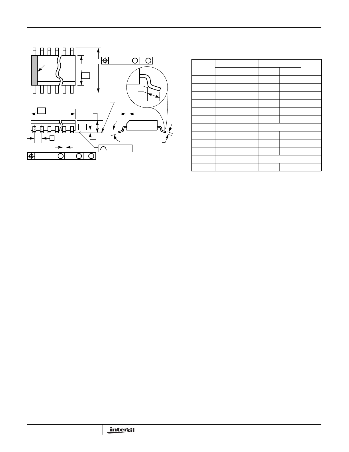
Small Outline Plastic Packages (SOIC)
ISL6559
N
INDEX
AREA
123
-A-
E
-B-
SEA TING PLANE
D
A
-C-
0.25(0.010) BM M
H
L
h x 45
o
α
e
B
0.25(0.010) C AM BS
M
NOTES:
1. Symbols are defined in the “MO Series Symbol List” in Section 2.2
of Publication Number 95.
2. Dimensioning and tolerancing per ANSI Y14.5M-1982.
3. Dimension “D” does not include mold flash, protrusions or gate
burrs. Mold flash, protrusion and gate burrs shall not exceed
0.15mm (0.006 inch) per side.
4. Dimension “E” does not include interlead flash or protrusions. Interlead flash and protrusions shall not exceed 0.25mm (0.010
inch) per side.
5. The chamfer on the body is optional. If it is not present, a visual
index feature must be located within the crosshatched area.
6. “L” is the length of terminal for soldering to a substrate.
7. “N” is the number of terminal positions.
8. Terminal numbers are shown for reference only.
9. The lead width “B”, as measured 0.36mm (0.014 inch) or greater
above the seating plane, shall not exceed a maximum value of
0.61mm (0.024 inch)
10. Controlling dimension: MILLIMETER. Converted inch dimensions are not necessarily exact.
A1
0.10(0.004)
M28.3 (JEDEC MS-013-AE ISSUE C)
28 LEAD WIDE BODY SMALL OUTLINE PLASTIC PACKAGE
INCHES MILLIMETERS
SYMBOL
A 0.0926 0.1043 2.35 2.65 -
A1 0.0040 0.0118 0.10 0.30 -
B 0.013 0.0200 0.33 0.51 9
C 0.0091 0.0125 0.23 0.32 D 0.6969 0.7125 17.70 18.10 3
E 0.2914 0.2992 7.40 7.60 4
e 0.05 BSC 1.27 BSC H 0.394 0.419 10.00 10.65 -
C
h 0.01 0.029 0.25 0.75 5
L 0.016 0.050 0.40 1.27 6
N28 287
o
α
0
o
8
o
0
o
8
Rev. 0 12/93
NOTESMIN MAX MIN MAX
-
20
FN9084.8
December 29, 2004
Page 21

ISL6559
Quad Flat No-Lead Plastic Package (QFN)
Micro Lead Frame Plastic Package (MLFP)
L32.5x5
32 LEAD QUAD FLAT NO-LEAD PLASTIC PACKAGE
(COMPLIANT TO JEDEC MO-220VHHD-2 ISSUE C
MILLIMETERS
SYMBOL
A 0.80 0.90 1.00 A1 - - 0.05 A2 - - 1.00 9
A3 0.20 REF 9
b 0.18 0.23 0.30 5,8
D 5.00 BSC D1 4.75 BSC 9
D2 2.95 3.10 3.25 7,8
E 5.00 BSC E1 4.75 BSC 9
E2 2.95 3.10 3.25 7,8
e 0.50 BSC -
k0.25 - - -
L 0.30 0.40 0.50 8
L1 - - 0.15 10
N322
Nd 8 3
Ne 8 8 3
P- -0.609
θ --129
NOTES:
1. Dimensioning and tolerancing conform to ASME Y14.5-1994.
2. N is the number of terminals.
3. Nd and Ne refer to the number of terminals on each D and E.
4. All dimensions are in millimeters. Angles are in degrees.
5. Dimension b applies to the metallized terminal and is measured
between 0.15mm and 0.30mm from the terminal tip.
6. The configuration of the pin #1 identifier is optional, but must be
located within the zone indicated. The pin #1 identifier may be
either a mold or mark feature.
7. Dimensions D2 and E2 are for the exposed pads which provide
improved electrical and thermal performance.
8. Nominal dimensions are provided to assist with PCB Land Pattern
Design efforts, see Intersil Technical Brief TB389.
9. Features and dimensions A2, A3, D1, E1, P & θ are present when
Anvil singulation method is used and not present for saw
singulation.
10. Depending on the method of lead termination at the edge of the
package, a maximum 0.15mm pull back (L1) maybe present. L
minus L1 to be equal to or greater than 0.3mm.
NOTESMIN NOMINAL MAX
Rev. 1 10/02
All Intersil U.S. products are manufactured, assembled and tested utilizing ISO9000 quality systems.
Intersil Corporation’s quality certifications can be viewed at www.intersil.com/design/quality
Intersil products are sold by description only. Intersil Corporation reserves the right to make changes in circuit design, software and/or specifications at any time without
notice. Accordingly, the reader is cautioned to verify that data sheets are current before placing orders. Information furnished by Intersil is believed to be accurate and
reliable. However, no responsibility is assumed by Intersil or its subsidiaries for its use; nor for any infringements of patents or other rights of third parties which may result
from its use. No license is granted by implication or otherwise under any patent or patent rights of Intersil or its subsidiaries.
For information regarding Intersil Corporation and its products, see www.intersil.com
21
FN9084.8
December 29, 2004
Page 22

 Loading...