

Page 1
®
ISL6534
Data Sheet December 21, 2004 FN9134.1
Dual PWM with Linear
The ISL6534 is a versatile triple regulator that has two
independent synchronous-rectified buck controllers with
integrated 12V gate drivers (OUT1 and OUT2) and a linear
controller (OUT3) to offer precision regulation of up to three
voltage rails. An optional shunt regulator allows 12V only
operation, when a 5V supply is not available.
Each controller has independent soft-start and enable
functions combined on a single pin. A capacitor from each
SS/EN pin to ground sets the soft-start time, and pulling
SS/EN below 1.0V disables the controller. The SS/EN pins
can be controlled independently or they can be ganged
together to provide complete control of start-up coordination.
The PGOOD function indicates when all regulators have
completed their soft start and provides an indication of shortcircuit conditions on either switching regulator.
There are two ways to control the switching frequency of the
PWM regulators. The default switching frequency is 300kHz
(FS_SYNC pin open). A resistor from FS_SYNC to ground
increases the switching frequency (up to 1MHz). Connecting
the gate signal from another PWM IC synchronizes the
ISL6534 switchers to the frequency of the other controller.
This allows independent regulators operating at a common
frequency to avoid low-frequency beats. The gate drivers for
DDR mode can be staggered by 90° in order to minimize
cross-conduction.
Switcher OUT1 has an internal 0.8% accurate reference for
regulating any voltage down to 0.6V. OUT2 has current
sinking capability and an external reference input allowing
convenient connection to OUT1 through a resistor divider for
DDRAM applications. The 3.3V reference pin provides the
option for independent regulation of OUT2. The linear
controller drives an external N-Channel MOSFET, making
the ISL6534 one of the most versatile regulators available.
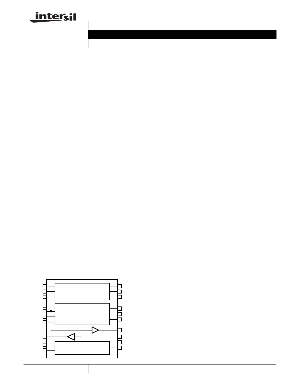
Simplified Block Diagram
SS1/EN1
COMP1
FB1
OUT1
PWM CONTROLLER
BOOT1
UGATE1
LGATE1
Features
• Two Synchronous-Rectified Buck Controllers
- Voltage Mode control
- VIN range up to 12V
- VOUT range from 0.6V to 6V
- 12V LGATE drivers; up to 12V Boot Strap for UGATE
• Switcher References
- 0.6V Reference for OUT1 (0.8% Accurate)
- 3.3V Reference Output for OUT2 (0.8% Accurate)
- External Reference Input for OUT2
- Buffered VTT Reference Output
• Switcher clocking
- Phase options for Optimal Clock Relationship
- Resistor-Selectable Switching Frequency (300kHz
default; Resistor to Ground for 300kHz to 1MHz range)
- Synchronization-Capable Switching Frequency
(Connect FS_SYNC to Separate Regulator)
• Single Linear Controller
- Drives N-Channel MOSFET
- 0.6V Reference (0.8% Accurate)
- VIN range up to 12V
- VOUT range from 0.6V to 6V
• 12V and 5V supplies required (but optional shunt regulator
can generate VCC = 5.8V from 12V)
• Three Independent Soft-Start/Enable Pins
- Gang Together or Contro l Independently
• PGOOD Output Indicates All Outputs Available
• Thermally Enhanced QFN or TSSOP Package
• QFN Package:
- Compliant to JEDEC PUB95 MO-220
QFN - Quad Flat No Leads - Package Outline
- Near Chip Scale Package footprint, which improves
PCB efficiency and has a thinner profile
• Pb-Free Available (RoHS Compliant)
SS2/EN2
REFIN
FB2
COMP2
VREF
SS3/EN3
FB3
OUT2
PWM CONTROLLER
3.3V
OUT3
LINEAR CONTROLLER
1
BOOT2
UGATE2
LGATE2
REFOUT
PGOOD
FS/SYNC
DRIVE3
CAUTION: These devices are sensitive to electrostatic discharge; follow proper IC Handling Procedures.
1-888-INTERSIL or 321-724-7143
| Intersil (and design) is a registered trademark of Intersil Americas Inc.
All other trademarks mentioned are the property of their respective owners.
Copyright Intersil Americas Inc. 2004. All Rights Reserved
Page 2
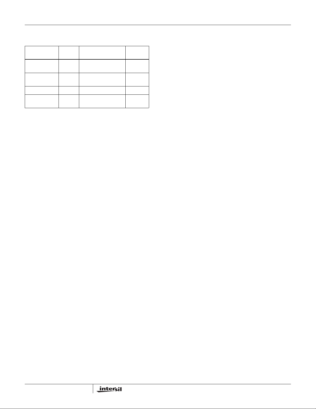
Ordering Information
ISL6534
TEMP.
PART NUMBER
ISL6534CV 0 to 70 24 Ld EPTSSOP
ISL6534CVZ
(See Note)
ISL6534CR 0 to 70 32 Ld 5x5 QFN L32.5x5
ISL6534CRZ
(See Note)
NOTE: Intersil Pb-free products employ special Pb-free material
sets; molding compounds/die attach materials and 100% matte tin
plate termination finish, which are RoHS compliant and compatible
with both SnPb and Pb-free soldering operations. Intersil Pb-free
products are MSL classified at Pb-free peak reflow temperatures that
meet or exceed the Pb-free requirements of IPC/JEDEC J STD020C.
Add “-T” suffix for tape and reel.
(°C) PACKAGE
(exposed pad)
0 to 70 24 Ld EPTSSOP
(exposed pad) (Pb-free)
0 to 70 32 Ld 5x5 QFN
(Pb-free)
PKG. DWG.
#
M24.173B
M24.173B
L32.5x5
Pinouts (see Pin Descriptions, page 9)
2
FN9134.1
Page 3
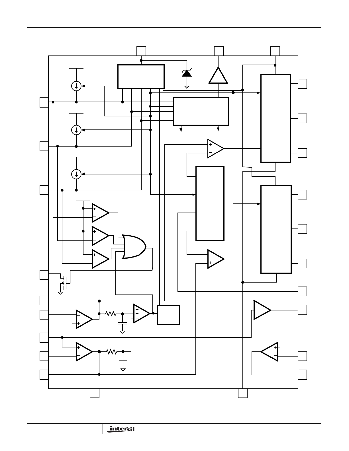
Block Diagram
VCC
ISL6534
VREF
VCC12
SS1/EN1
SS2/EN2
SS3/EN3
VCC5
VCC5
VCC5
30 µA
30
30 µA
3.3V
µA
POWER
ON
RESET
AND CONTROL
PGOOD =
all 3 SS ramps done
with no COMP short
VCC5
5.8V
REFERENCE
BIAS CURRENT
0.6V
3.3V
CLOCK AND
SAWTOOTH
GENERAT OR
3.3V
OUTPUT1
DRIVERS
GATE CONTR OL
LOGIC
DEAD-TIME
CONTROL
OUTPUT2
DRIVERS
GATE CONTRO L
LOGIC
DEAD-TIME
CONTROL
BOOT1
UGATE1
LGATE1
BOOT2
UGATE2
PGOOD
COMP1
FB1
REFIN
FB2
COMP2
0.6V
LGATE2
FS/SYNC
3.3V
MONITOR
COMP PINS
FOR SHORTS
1-2 CLOCK
CYCLE
FILTER
IF SHORT > FIL T ER,
SHUT DOWN ALL
3 OUTPUTS
0.6V
PGND GND
REFOUT
FB3
DRIVE3
FIGURE 1. BLOCK DIAGRAM
3
FN9134.1
Page 4
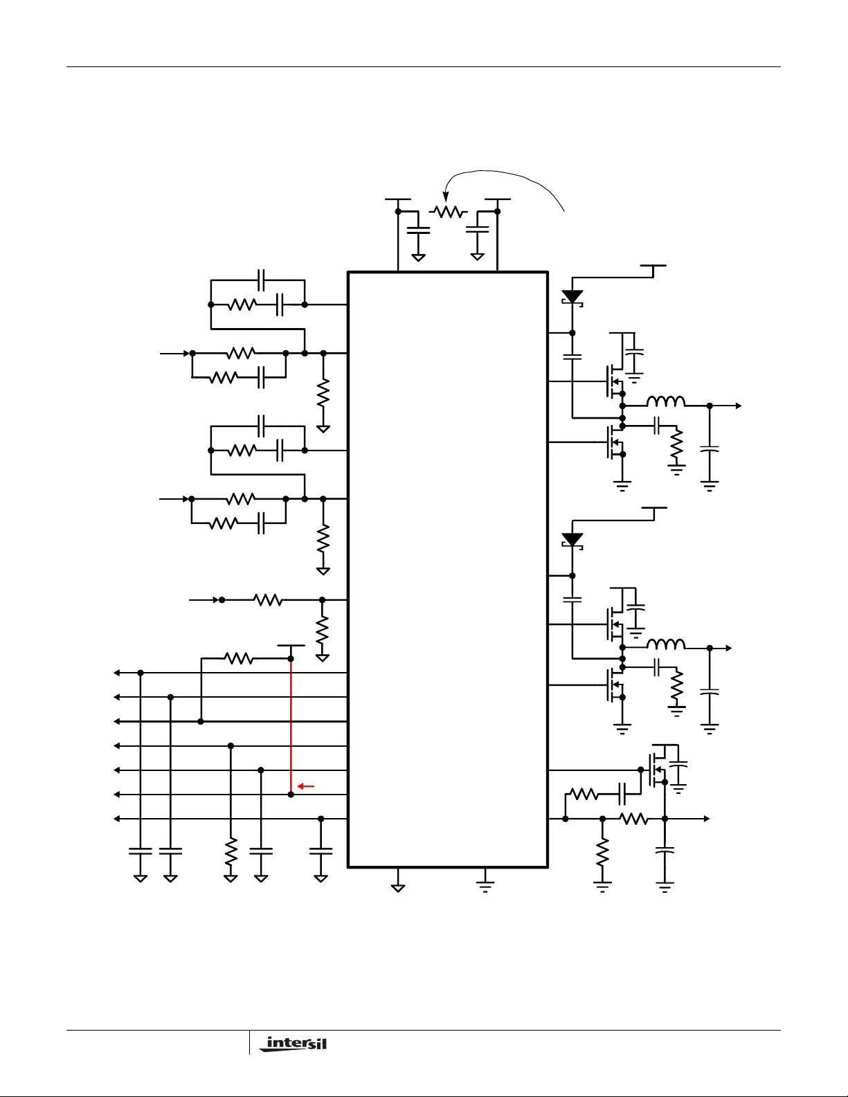
Typical Application, DDRAM Controller
VOLTAGE INPUTS REQUIRED
VCC12 (12V)
VCC (5V OR 5.8V FROM SHUNT)
VIN1, VBS1
VIN2, VBS2
VIN3
COMP1
VOUT1
FB1
ISL6534
ISL6534
DDR MODE
VCC
VCC
VCC12
OPTIONAL R FOR
SHUNT REGULATOR
VCC12
BOOT1
VBS1
VOLTAGE OUTPUTS
VOUT1
VOUT2
VOUT3
VCC12
VIN1
VTTREF
VOUT2
VOUT1 (DDR)
VREF
VCC
DDR
COMP2
FB2
REFIN
REFOUT
VREF
PGOOD
FS/SYNC
SS1/EN1
SS2/EN2
ISL6534
UGATE1
LGATE1
BOOT2
UGATE2
LGATE2
DRIVE3
VOUT1
VCC12
VBS2
VIN2 = VOUT1 (DDR)
OR OTHER
VOUT2
VIN3
NOTE: Not all components are necessary in all applications.
FIGURE 2. TYPICAL APPLICATION, DDRAM CONTROLLER
4
SS3/EN3
GND
PGND
FB3
VOUT3
FN9134.1
Page 5
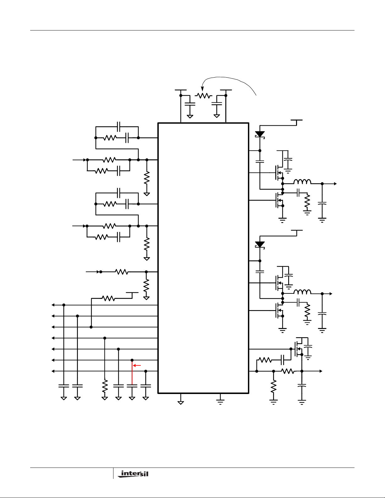
Typical Application, Independent Mode
VOLTAGE INPUTS REQUIRED
VCC12 (12V)
VCC (5V OR 5.8V FROM SHUNT)
VIN1, VBS1
VIN2, VBS2
VIN3
COMP1
VOUT1
FB1
ISL6534
ISL6534
INDEPENDENT MODE
VCC
VCC
VCC12
VCC12
OPTIONAL R FOR
SHUNT REGULATOR
VBS1
BOOT1
VOLTAGE OUTPUTS
VOUT1
VOUT2
VOUT3
VCC12
VIN1
VTTREF
VOUT2
VREF (IND)
VREF
VCC
IND
COMP2
FB2
REFIN
REFOUT
VREF
PGOOD
FS/SYNC
SS1/EN1
SS2/EN2
SS3/EN3
ISL6534
UGATE1
LGATE1
BOOT2
UGATE2
LGATE2
DRIVE3
FB3
VBS2
VOUT1
VCC12
VIN2
VOUT2
VIN3
VOUT3
NOTE: Not all components are necessary in all applications.
FIGURE 3. TYPICAL APPLICATION, INDEPENDENT MODE
5
GND
PGND
FN9134.1
Page 6
ISL6534
Absolute Maximum Ratings Thermal Information
Supply Voltage (VCC12) . . . . . . . . . . . . . . . . . GND - 0.3V to 14.0V
Supply Voltage (VCC, separate supply). . . . . . . GND - 0.3V to 5.5V
Supply Voltage (VCC, shunt regulator) . . . . . . . GND - 0.3V to 6.0V
UGATE1, UGATE2, BOOT1, BOOT2. . . . . . . . . . GND - 0.3V to 30V
LGATE1, LGATE2, DRIVE3. . . . . . . . . . . . . . GND - 0.3V to VCC12
FS_SYNC (through 10K resistor). . . . . . . . . . . . .GND - 0.3V to 12V
REFIN, REFOUT, PGOOD, VREF. . . . . . . . . . . GND - 0.3V to VCC
FB1, COMP1, FB2, COMP2, FB3 . . . . . . . . . . . GND - 0.3V to VCC
SS1/EN1, SS2/EN2, SS3/EN3. . . . . . . . . . . . . . GND - 0.3V to VCC
PGND. . . . . . . . . . . . . . . . . . . . . . . . . . . GND - 0.3V to GND + 0.3V
ESD Rating
Human Body Model (Per MIL-STD-883 Method 3015.7). . .1500V
Machine Model (Per EIAJ ED-4701 Method C-111). . . . . . . .100V
Charged Device Model (Per EOS/ESD DS5.3, 4/14/93) . . .1000V
Operating Conditions
Temperature Range . . . . . . . . . . . . . . . . . . . . . . . . . . . . 0°C to 70°C
VCC12 Supply Voltage Range (Typical) . . . . . . . . . . . . . 12V ±1.2V
VCC Supply Voltage Range (Typical) . . . . . . . . . . . . . . . . 5V ±0.5V
VCC Shunt Regulator Voltage Range (Typical) . . . . . . . 5.8V ±0.2V
CAUTION: Stresses above those listed in “Absolute Maximum Ratings” may cause permanent damage to the device. This is a stress only rating and operation of the
device at these or any other conditions above those indicated in the operational sections of this specification is not implied.
NOTE:
is measured in free air with the component mounted on a high effective thermal conductivity test board with “direct attach” features. See
1. θ
JA
Tech Brief TB379.
2. For θ
, the “case temp” location is the center of the exposed metal pad on the package underside.
JC
Thermal Resistance θ
EPTSSOP Package (Notes 1, 2) . . . . . 37 4
QFN Package (Notes 1, 2). . . . . . . . . . 32 4
Maximum Power Dissipation. . . . . . . . . . . . . . . . . . . . . . . . . . . . . .___W
Maximum Junction Temperature (Hermetic P ac ka ge or Die) . . . 175°C
Maximum Junction Temperature (Plastic Package) . . . . . . . . 150°C
Maximum Storage Temperature Range. . . . . . . . . . .-65°C to 150°C
Maximum Lead Temperature (Soldering 10s) . . . . . . . . . . . . . 300°C
(°C/W) θJC (°C/W)
JA
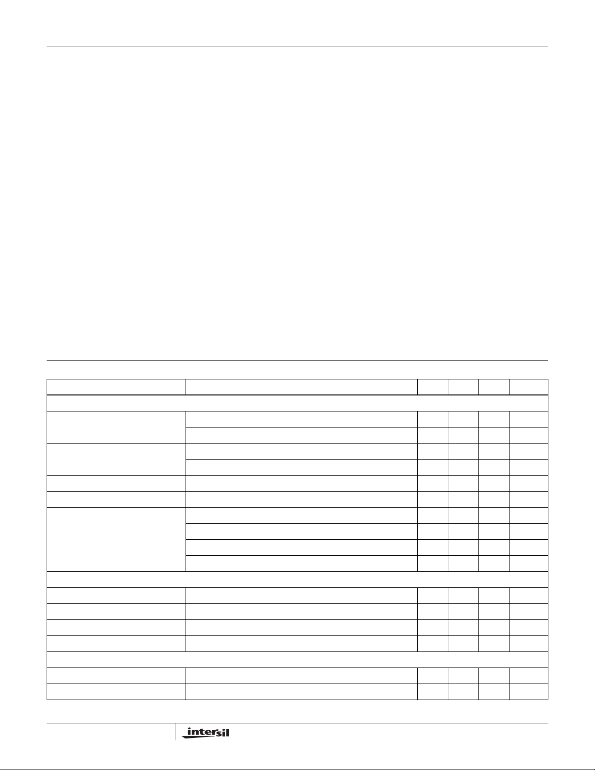
Electrical Specifications Operating Conditions: V
PARAMETER TEST CONDITIONS MIN TYP MAX UNITS
INPUT SUPPLY POWER
Input Supply Current (Quiescent) VCC; outputs disabled 4 mA
VCC12; outputs disabled 6 mA
Input Supply Current (Dynamic) VCC12; UGATEs, LGATEs CL = 1nF, 300kHz 50 mA
VCC; UGATEs, LGATEs CL = 1nF, 300kHz 7 mA
Shunt Regulator Output Voltage 40mA current; ~equivalent to 150Ω resistor VCC to 12V 5.6 5.8 6.0 V
Shunt Regulator Current 150Ω resistor VCC to 12V 40 mA
Power-On Reset Threshold VCC Rising 4.15 4.23 4.4 V
VCC Falling 3.9 4.0 4.15 V
VCC12 Rising 7.8 V
VCC12 Falling 7.3 V
SYSTEM ACCURACY
Outputs 1 and 3 Reference Voltage 0.6 V
Output 2 Reference Voltage 3.3V
Outputs 1 and 2 System Accuracy (Note 3) -0.8 0.8 %
Output 3 System Accuracy (Note 3) -0.8 0.8 %
OSCILLATOR
Accuracy -20 20 %
Frequency FS_SYNC pin open 240 300 360 kHz
= 5V, V
CC
= 12V, TA = 0°C to 70°C, Unless Otherwise Specified
CC12
6
FN9134.1
Page 7
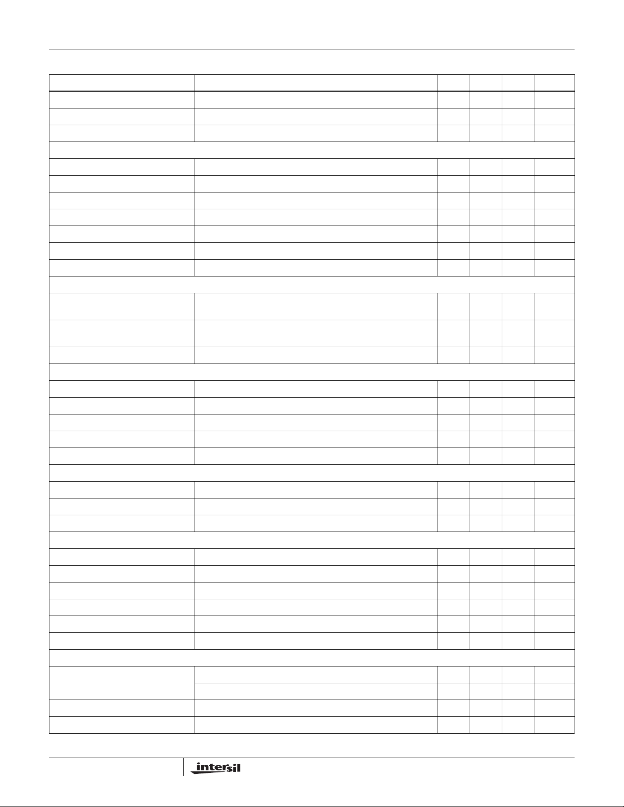
ISL6534
Electrical Specifications Operating Conditions: V
PARAMETER TEST CONDITIONS MIN TYP MAX UNITS
Adjustment Range FS_SYNC pin: resistor to GND; see Figure 12 for curves 300 1000 kHz
Sawtooth Amplitude 2.1 V
Duty-Cycle Range 0 87.5 %
ERROR AMPLIFIER (OUT1 and OUT2)
Open-Loop Gain RL = 10kΩ to ground; (Note 5) 85 dB
Open-Loop Bandwidth CL = 100pF, RL = 10kΩ to ground; (Note 5) 15 MHz
Slew Rate CL = 100pF, RL = 10kΩ to ground; (Note 5) 4 V/µs
EA Offset COMP1/2 to FB1/2; compare to internal VREF/REFIN 2 mV
Maximum Output Voltage RL = 10kΩ to ground; (may trip short-circuit) 3.6 4.1 V
Output High Source Current COMP1/2 -8 mA
Output Low Sink Current COMP1/2 6 mA
PROTECTION AND MONITOR
Under-Voltage Threshold (COMP1 and
COMP2)
UV filter time based on internal oscillator clock frequency
PGOOD Low Voltage IPGOOD = 2mA 0.1 0.3 V
LINEAR REGULATOR (OUT3)
Output Voltage (As determined by resistor divider into FB3) 0.6 3.3 V
EA Offset DRIVE3 to FB3; compare to internal VREF 2 mV
DRIVE3 High Output Voltage 9V
DRIVE3 High Output Source Current 0.4 mA
DRIVE3 Low Output Sink Current 0.4 mA
VREF
Output Voltage 1.1µF max capacitance 3.3 V
Output Accuracy -0.8 +0.8 %
Source Current 2.0 mA
REFOUT (VTTREF)
Output Voltage Determined by REFIN voltage 0.6 3.3 V
Offset Voltage -10 +10 mV
Source Current 0.2 20 mA
Sink Current 0.48 mA
Output Capacitance 0.4 2.2 µF
Output High Voltage Minimum To select 0 degree phase; see Table 1 4.7 VCC V
ENABLE/SOFTSTART (SS/EN 1, 2, 3)
Enable Threshold EN Rising 1.05 V
Noise Immunity (noise de-glitch) 6µs
Soft-Start Current -30 µA
Causes PGOOD to go low; if there for a filter time,
Implies the COMP pin(s) is out -of-range, and shuts down IC
(nominal 300kHz = 3.3µs clock period)
EN falling 0.95
= 5V, V
CC
= 12V, TA = 0°C to 70°C, Unless Otherwise Specified (Continued)
CC12
3.3 V
12clock
pulses
7
FN9134.1
Page 8
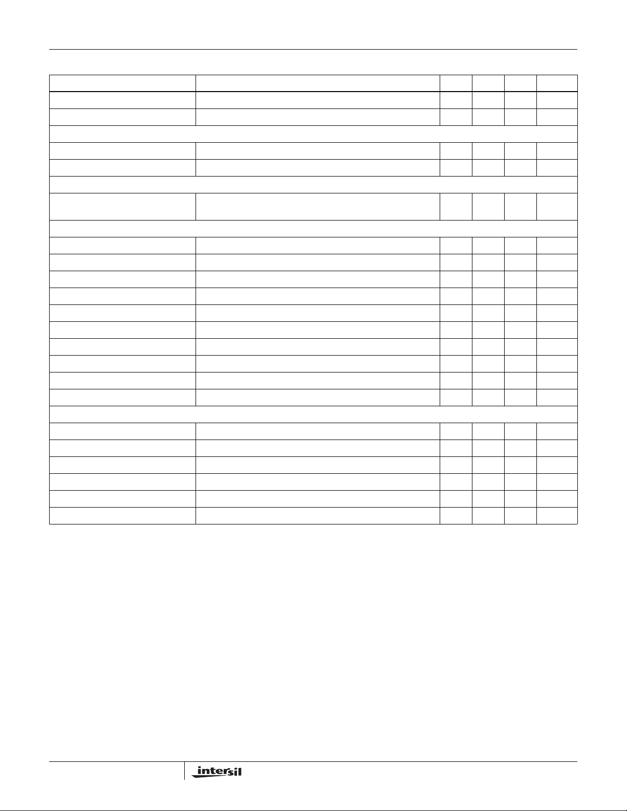
ISL6534
Electrical Specifications Operating Conditions: V
PARAMETER TEST CONDITIONS MIN TYP MAX UNITS
Soft-Start High Voltage End of ramp 3.3V V
Output High Voltage To select DDR mode; see Table 1 4.7 VCC V
FS/SYNC PLL
Frequency range of Lock-in 350 850 kHz
High Voltage Use a 10K series resistor (from LG pin of another IC, for example) 12 V
BOOT PINS (BOOT1, 2)
High Voltage Voltage with respect to GND; also depends upon VIN, Phase,
VOUT, and threshold of NFET
GATE DRIVERS
Output High Source Current UGATE1, UGATE2 1.5 A
Output High Source Current LGATE1, LGATE2 1.5 A
Output Low Sink Current UGATE1, UGATE2 1.5 A
Output Low Sink Current UGATE1, UGATE2 1.5 A
Output Voltage UGATE1, UGATE2 30 V
Output Voltage LGATE1, LGATE2 12 V
Upper Driver Source Resistance UGATE1, UGATE2 = 3V; BOOT = 12V 2 Ω
Lower Driver Source Resistance LGATE1, LGATE2 = 3V 2 Ω
Upper Driver Sink Resistance UGATE1, UGATE2 = 3V; BOOT = 12V 2.8 Ω
Lower Driver Sink Resistance LGATE1, LGATE2 = 3V 2.8 Ω
GATE DRIVERS SWITCHING TIME
UGATE Rise Time 10% - 90%; 2nF Load; BOOT = 12V 17 ns
UGATE Fall Time 90% - 10%; 2nF Load; BOOT = 12V 17 ns
UGATE Rise Time 10% - 90%; 2nF Load; BOOT = 24V 27 ns
UGATE Fall Time 90% - 10%; 2nF Load; BOOT = 24V 25 ns
LGATE Rise Time 10% - 90%; 2nF Load 17 ns
LGATE Fall Time 90% - 10%; 2nF Load 17 ns
NOTES:
3. Operating range is: 12V ±10%; 5V ±10%.
4. Thermal comments.
5. Guaranteed by design.
= 5V, V
CC
= 12V, TA = 0°C to 70°C, Unless Otherwise Specified (Continued)
CC12
830V
8
FN9134.1
Page 9
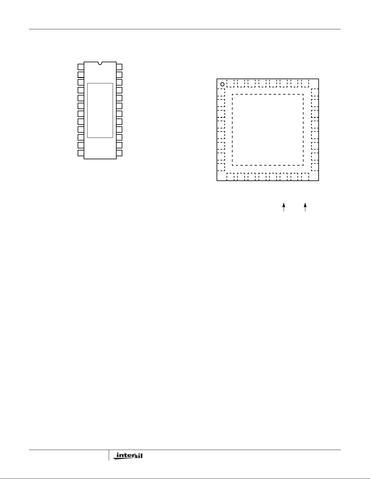
Pin Description
24-PIN TSSOP
TOP VIEW
ISL6534
32 LD 5x5 QFN
TOP VIEW
FB1
COMP1
COMP2
FB2
REFIN
REFOUT
SS1/EN1
SS2/EN2
SS3/EN3
VREF
DRIVE3
FB3
1
2
3
4
5
6
7
8
9
10
11
12
GND
BOTTOM
SIDE PAD
24
VCC
23
BOOT1
22
UGATE1
21
VCC12
20
LGATE1
19
LGATE2
18
PGND
17
UGATE2
16
BOOT2
15
GND
14
PGOOD
13
FS_SYNC
COMP2
FB3
COMP1
GND
BOTTOM
SIDE PAD
FS_SYNC
FB1
PGOOD
VCC
GND
NC
UGATE2
NC
NC
REFIN
NC
REFOUT
SS1/EN1
SS2/EN2
SS3/EN3
VREF
DRIVE3
FB2
FB2
32 31 30 29 28 27 26 25
1
2
3
4
5
6
7
8
9 10111213141516
NC
NOTES:
6. BOOT2 and UGATE2 are different order in QFN.
7. NC is No Connect
BOOT1
24
UGATE1
23
PGND_1
22
VCC12_1
21
LGATE1
20
LGATE2
19
VCC12_2
18
PGND_2
17
NC
BOOT2
VCC
This power pin supplies bias to the control functions. It can
be connected to a nominal 5V (±10%) supply, or it can
function as a shunt regulator (nominal 5.8V), with an external
pull-up resistor (nominally 150Ω to 12V).
GND
This pin is the signal ground for the IC. The metal thermal
pad under both packages is connected to the GND potential
(through the IC substrate; the pad does NOT substitute for
the GND pin connection). But the GND pin and the metal
pad should be connected together on the board, and tied to
a good GND plane (both for electrical and thermal
conduction). Note that the thermal pad on both packages
limits metal interconnect traces underneath the package.
VCC12 (QFN: VCC12_1, VCC12_2)
This power pin (nominal 12V) supplies the output gate
drivers, as well as some other control functions.
The QFN package has two power pins; one for each
switcher. The y are electrically connected internally, b ut allow
for separate decoupling caps to better isolate the switching
noise, if necessary. Ev en if they share one capacitor, they
should both be connected externally, for lower resistance.
PGND (QFN: PGND_1, PGND_2)
This pin is the Power GND for the gate drive circuits. It is not
directly tied to GND inside the IC; it should be tied to GND
on the board.
The QFN package has two Power GNDs; one local to each
switcher; both should be connected externally to the GND
plane on the board.
SS1/EN1, SS2/EN2, SS3/EN3
These analog input pins have two functions. A 30µA current
source charges an external capacitor (to GND), to provide a
soft-start timing ramp; their respective Output voltage will
follow the ramp voltage as it powers up . The 2nd function is
Enable; when the input is left open (with the soft-start cap),
the respective output will be Enabled after the ramp reaches
the 1V level. If the input is pulled to a low logic level, the
output will be disabled.
SS2/EN2 also has a special mode function; see Table 1.
Tying it to VCC (5V) selects the DDR mode (where both
OUT1 and OUT2 share the SS1 ramp); otherwise it will be in
the Independent mode.
COMP1, COMP2
These analog output pins are used to externally compensate
the error amplifiers for their respective regulators.
9
FN9134.1
Page 10

ISL6534
FB1, FB2, FB3
These analog input pins are used to set their respective
regulator output voltages. A resistor divider from the output
to GND is compared to a reference voltage (0.6V for OUT1
and OUT3; REFIN pin for OUT2). The compensation
components also connect to these pins.
UGATE1, UGATE2
These output pins provide the gate drive for the upper
MOSFETs of OUT1 and OUT2 respectively; the voltage
comes from its bootstrap pin, typically 12V (minus the diode
drop) above the VCC12 pin.
LGATE1, LGATE2
These output pins provide the gate drive for the lower
MOSFETs of OUT1 and OUT2 respectively; the voltage
comes from VCC12.
BOOT1, BOOT2
These pins feed the bootstrap voltage (externally generated
with a diode and a capacitor) to the upper MOSFETs,
through the UGA TE pins. Either BOO T pin can be connected
directly to a power supply instead (but only if the VIN voltage
of the regulator is sufficiently lower than that supply, such
that the FETs have enough gate-source voltage).
REFIN
This analog input is used as the reference voltage for OUT2
(the error amplifier compares it to the feedback resistor
divider). This voltage is also fed into a buffer, which is output
on the REFOUT pin.
REFOUT (VTT Buffer)
This analog output provides a buffered version of the REFIN
input, to be used by other IC’s in the system. In the DDR
mode, where VTT is generated from VDDQ, this output can
be used as a VTT Buffer.
In addition, it can be used to select the phase relationship,
but it disables the buffer in that case (see Table 1). Tying it to
VCC (5V) selects 0 degrees phase (in either mode); leaving
it open (where it can also be used as a reference output)
selects 90 degrees phase (in DDR mode) and 180 degrees
phase (in Independent Mode). A capacitor to GND is
recommended for stability (see Application Considerations).
VREF
This analog output pin is a 3.3V reference, which can be
used by this IC (or others) as a voltage reference. A
capacitor to GND is recommended for stability (see
Application Considerations).
DRIVE3
This pin drives the gate of an external N-Channel MOSFET,
for OUT3, which is a linear regulator.
PGOOD
This digital output is an open-drain pull-down device. When
power is first applied to the IC, the output is pulled low, for
power “Not Good”. After all 3 Soft-Start pins complete their
ramp up with no faults (no short detected on switchers) the
power is considered “Good”, and the output pin is highimpedance (to be pulled up to a logic high level with an
external pull-up resistor). See the PGOOD section under
Functional Description for more details.
FS/SYNC
This input allows the user to adjust the internal oscillator
used for the PWM outputs; a pull-down resistor will speed up
the oscillator. In addition, a digital clock signal can be fed into
this input, in order to SYNC its clock with the external one;
this allows the clock edges to line up in a way that won’t
interfere with each.
PINOUT NOTE:
Note that the pin order of UGATE2 and BOOT2 are different in the
two packages, due to bonding optimization. The QFN package also
adds an extra VCC12 and PGND pin, and has additional No
Connection pins.
Functional Description
Overview
There are two single-phase synchronous buck converters,
and one linear regulator. Except for a common cloc k, the two
PWM regulators are independent. Refer to Figures 2 and 3
for a quick discussion of the circuit. The right side of the
diagram shows the 3 output stages with their components;
each switcher has an upper and lower FET, input capacitor,
bootstrap diode and capacitor, an LC output filter, and an
optional snubber.
The 3rd regulator (OUT3) is a linear, with an external NFET,
input and output capacitor. The output voltage is divided to
FB3, and compared to an internal 0.6V reference. An RC is
used for compensation.
The left side of the diagrams show the various control and
programming components. Each switcher has a compensation
network for stability that includes the output resistor divider.
VREF and REFOUT can be used as reference voltages. There
are three SS/EN pins to set the soft-start ramp of each output,
and a PGOOD output to signal when they are all done. The
FS_SYNC pin allows options for the oscillator frequency. Each
of these features will be described in more detail, either in the
Functional Description or the Application Considerations.
The first regulator (OUT1) has an internal 0.6V reference. To
set the output voltage level, connect a resistor divider
between VOUT1 and FB1.
The second regulator (OUT2) requires an external reference
connected to REFIN. For DDR memory applications
(Figure 2), connect a divide-by-two resistor divider from
VOUT1 to ground with the center point connected to REFIN.
10
FN9134.1
Page 11
ISL6534
This causes VOUT2 to track VOUT1 at one-half its value.
Connect VOUT2 to FB2 (through the compensation resistor).
A buffered copy of REFIN is provided on REFOUT.
For Independent mode operation on OUT2 (Figure 3), a 3.3V
reference is provided on VREF which can be used directly , or
divided down for REFIN. A resistor divider from VOUT2 to
FB2 sets the output voltag e.
Operational Modes
Table 1 shows how to select the various modes and phasing
between the two switching regulators.
TABLE 1. MODE AND PHASE SELECTION
MODE EN_SS2 REFOUT PWM1/2 CH1/2
DDR VCC VCC 0 deg EN1/SS1 enables
CH1 and CH2
DDR VCC Open 90 deg “
Independent SS2 cap VCC 0 deg EN1/SS1 for Ch1;
EN2/SS2 for Ch2
Independent SS2 cap Open 180 deg “
DDR mode is chosen by connecting the SS2/EN2 pin to
VCC (5V). In this mode, SS1/EN1 is used to enable and softstart both OUT1 and OUT2 (note that only a single 30µA
current source is charging a single soft-start capacitor). In
addition, VOUT1 (usually divided by 2) can be used as the
REFIN for OUT2. VOUT1 is often used as VIN2 (especially
when the VOUT2 current is low enough) although it is not
necessary. And OUT2 does allow both sinking and sourcing
of current for the DDR.
For Independent mode, SS2/EN2 is not connected to VCC.
Instead it is connected to a soft-start capacitor to GND,
similar to SS1/EN1. The capacitors will ramp each output
independently, and each can be turned off by pulling its
SS/EN pin to GND; releasing will start a new soft-start ramp.
SS3/EN3 is also independent of the first two. As explained
earlier, one capacitor can be shared by more than one
SS/EN pin.
To select the Phase shift between Channel 1 and 2, the
REFOUT pin is used. Tie it to the VCC pin to get 0 degrees
in either mode (which means both switchers are in phase). In
this case, the REFOUT pin is not available for use
elsewhere; the buffer is disabled. Leave REFOUT open
(driven to whatever voltage is supplied at REFIN) and it
selects 90 degrees in the DDR mode, or 180 degrees in
Independent mode; REFOUT can be used as a reference in
this case. The advantage of Phase shift is to keep the
switching current spikes from lining up to create even higher
noise, or interaction between the channels; it also reduces
the RMS current through the input capacitors, allowing fewer
caps to be employed. However, depending on the VOUT to
VIN ratios of both, there is no guarantee that opposite edges
might not line up, depending on the duty cycles; so the user
should check for that possibility.
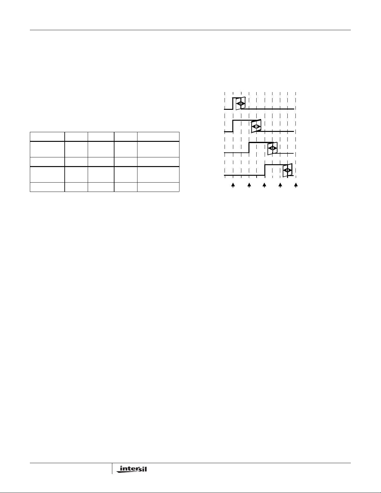
Figure 4 shows the phases. The rising edge of LGATE1
(LG1) and LGATE2 (LG2) is fixed; the phase difference is
relative to the rising edges. The falling edge of each is the
variable one (determined by the duty cycle). LG1 is shown
with a pulse width shorter than LG2; this is just an arbitrary
example, and it does not affect the rising edges.
LG1
LG2 (0 deg)
LG2 (90 deg)
LG2 (180 deg)
90 180 270 0
0
FIGURE 4. PHASE OF LG2 WITH RESPECT TO RISING EDGE
OF LG1
Output Regulation
The basic PWM regulator voltage is usually set up as
follows: FB and the internal reference are the two inputs to
the error amplifier, which are forced to be equal. The output
voltage is externally divided down to the FB pin, to equal the
reference. In the ISL6534, VOUT1 uses an internal 0.6V
reference; VOUT2 uses an external REFIN pin for the
reference. There are many variations of the above,
especially when the modes (Independent or DDR) are also
considered. Below are some of the cases that can be used,
along with the advantages or disadvantages of each.
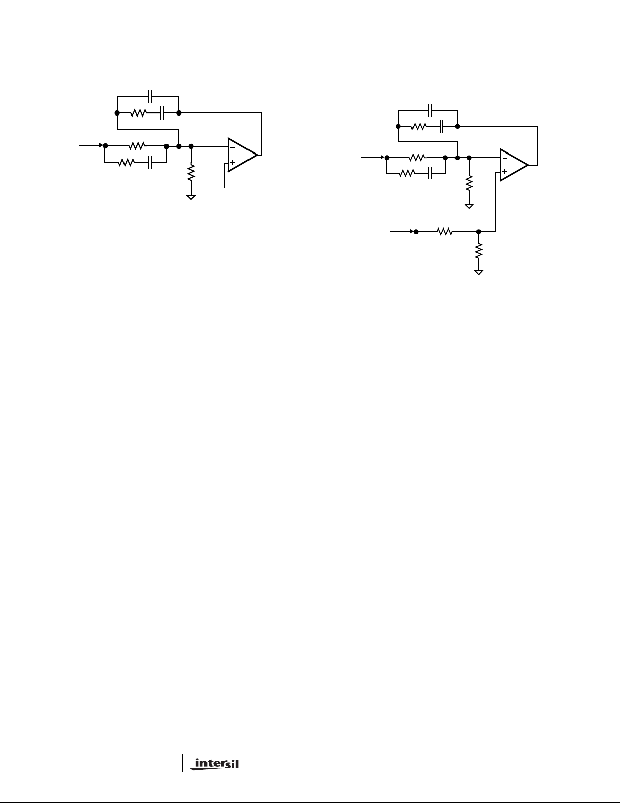
The following figures show the compensation circuit for
VOUT1 and VOUT2; the y include a full Type 3 compensation
network. Also shown is the resistor divider for REFIN.
Several notes:
1. The labeling of the resistors may not match other
diagrams; they should be used just for the equations
included.
2. The VREF pin (nominal 3.3V) is assumed here, but any
other appropriate fixed voltage reference can be used as
REFIN for OUT2.
3. One percent (or better) resistors are typically used for
these resistor dividers; the overall system accuracy
depends directly upon them. Exact ratios are not always
possible, due to the limited values of standard resistors
available; these errors must also be added to the
tolerance.
11
FN9134.1
Page 12
ISL6534
VOUT1 (INDEPENDENT OR DDR MODE)
COMP1
VOUT1
FIGURE 5. RESISTOR DIVIDER FOR VOUT1 (DDR OR
R5
INDEPENDENT MODE)
FB1
EA
R6
0.6V
Figure 5 shows the resistors for VOUT1.
Case 1 is the usual case, where R5 and R6 divide VOUT1
down to match the 0.6V internal reference. VOUT1 must be
greater than 0.6V; 2 resistors are needed, and their accuracy
directly affect the regulator tolerance.
Case 2 can be used only if VOUT1 equals exactly 0.6V ; then
no divider is needed; only one resistor (R5, which is part of
the compensation) is needed, and its accuracy does not
directly affect the output tolerance.
VOUT1 cannot be less than 0.6V.
Case 1 (divide VOUT1):
REF = 0.6V
FB1 = VOUT1*R6/(R5+R6)
Case 2 (no dividers):
REF = 0.6V
FB1 = VOUT1 (no R6 )
VOUT2 (INDEPENDENT MODE)
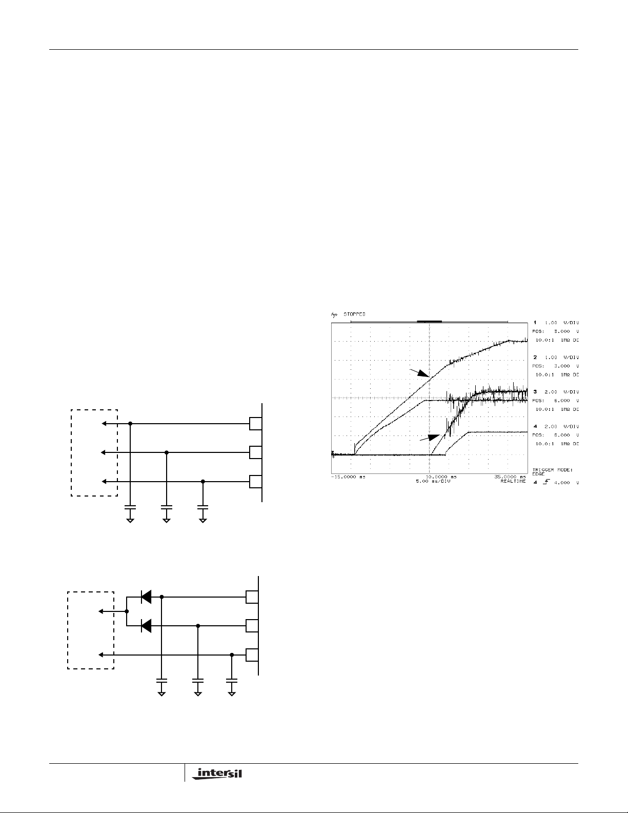
Figure 6 shows the resistors for VOUT2.
Case 1 is the most general case (no restriction on VREF > or
< VOUT2), and the most flexible. Both VREF and the output
are divided down to the same arbitrary reference (in the 0.6V
to 3.3V range for best performance). The advantage is that if
either the VREF or desired output voltage changes going
forward, the only board change needed is the value of 1 or
more resistors. The disadvantage is that since there are two
resistor dividers, both of them add to the error budget of the
regulator output. The total number of resistors used is 4.
Case 2 can be used when VOUT2 is less than VREF. R3 and
R4 divide the reference to match V OU T2. It saves a resistor
(R2); R1 (usually ~1kΩ) is still needed as part of the
compensation, but it doesn’t affect the accur acy of the output.
Three resistors are needed; this is the most typical case.
Case 3 can be used only when VOUT2 is greater than VREF,
which is brought directly into REFIN; then VOUT2 is divided
down to match it. Only two resistors (R1, R2) are needed,
and both affect the accuracy.
Case 4 can be used only if VREF = VOUT2; this case is the
most accurate (since neither has a divider), and only uses
one resistor (R1, as part of the compensation).
COMP2
VOUT2
VREF (IND)
OR
VOUT1 (DDR)
FIGURE 6. RESISTOR DIVIDERS FOR VOUT2 AND REFIN
R1
R3
FB2
EA
R2
REFIN
R4
Case 1 (divide both signals):
REFIN = VREF*R4/(R3+R4)
FB2 = VOUT2*R2/(R1+R2)
Case 2 (divide VREF):
REFIN = VREF*R4/(R3+R4)
FB2 = VOUT2 (no R2)
Case 3 (divide VO UT2):
REFIN = VREF (no R3, R4)
FB2 = VOUT2*R2/(R1+R2)
Case 4 (no dividers)
REFIN = VREF (no R3, R4)
FB2 = VOUT2 (no R2)
VOUT2 (DDR MODE)
The main difference for DDR Mode is that rather than using a
fixed external reference for REFIN, a reference based on
VOUT1 (which is also called VDDQ for DDR) is used
instead. See Figure 6.
Case 1 is again the most general case; Both VOUT1 and the
VOUT2 output are divided down to the same arbitrary
reference (in the 0.6V to 3.3V range for best performance).
The trade-offs are the same as Case 1 for Independent
mode described earlier.
Case 2 can be used when VOUT2 is less than VOU T1 ,
which is the case for DDR (since VOUT2 = 1/2 VOUT1). It
saves a resistor (R2); R1 is still needed as part of the
compensation, but it doesn’t affect the accuracy of the
output. R3 and R4 divide the VOUT1 by 2 to match VOUT2.
Three resistors are needed, two of which affect the accuracy.
Since the DDR mode almost always uses the divide by two,
no flexibility is lost here; just change the VOUT1 resistor
divider to change VDDQ, and VOUT2 will still track at 1/2 the
value.
12
FN9134.1
Page 13
ISL6534
Cases 3 and 4 don’t apply for DDR.
Case 1 (divide both signals):
REFIN = VOUT1*R4/(R3+R4)
FB2 = VOUT2*R2/(R1+R2)
Case 2 (divide VOUT1):
REFIN = VOUT1*R4/(R3+R4)
FB2 = VOUT2 (no R2 )
Soft-Start/Enable
Numerous combinations of independent and dependent
startup are possible by the various methods of connecting
the three EN/SS pins; some combinations are shown in
Figures 7 and 8. In Figure 7, the three regulators enable
independently and rise at rates selected by their individual
soft-start capacitors C
diodes are used to connect to a single open-drain pull-down
device (not shown); this allows one FET to disable both
channels. When enabled, they will each rise at their own
ramp rate. If they could use the same ramp rate, then both
pins could share one capacitor and the one FET, and the
diodes are not necessary. The 3rd channel is disabled and
ramped independently. Note that since the EN trip point is
around 1V, some care should be taken to guarantee the
diode drop and the FET in series with it will always be
below it.
OPEN-DRAIN
LOGIC SIGNALS
EN1
EN2
EN3
SS1
, C
SS2
, and C
. In Figure 8, two
SS3
SS1/EN1
SS2/EN2
SS3/EN3
ISL6534
The soft-start pins can share the same capacitor, to ramp
them all at the same rate (but since there will be 3 times the
current, the value of the capacitor needs to be approximately
3 times bigger, for the same ramp rate).
Note that each output rise does not start until its SS/EN
voltage reaches ~1V; the output will then start to ramp up
until the soft-start is > ~3.3V (ramp is done). PGOOD will not
go active unless all three ramps are >3.3V (and no faults are
detected).
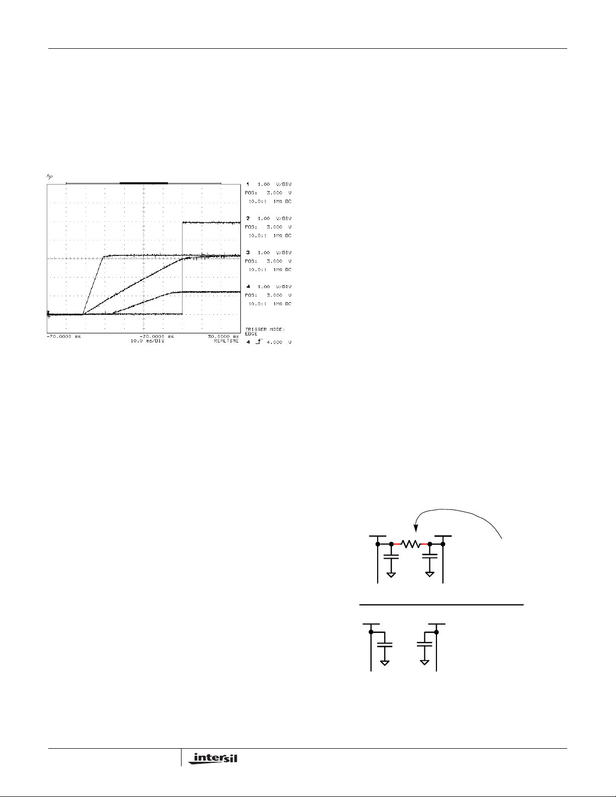
Figure 9 shows the start-up waveform for VO UT1 at power
up. In this example, the VCC voltage is generated from the
internal shunt regulator. The ramp of the 12V is controlled by
the external power supply; it can vary widely, depending
upon the type and model used. The ramp of the shunt more
or less follows the VCC12 until it reaches its regulation point
at ~5.8V. Both VCC and VCC12 must be past their rising
POR trip points before SS1 starts rising. The order doesn’t
matter, and may be different, especially when the VCC uses
an independent supply.
4: VCC12
VCC12 ~8V
2: SS1/EN1
3: VCC
SS1 ~1V
1: VOUT1
C
SS1
FIGURE 7. CONNECTIONS FOR INDEPENDENT ENABLE
AND SOFT-START
OPEN-DRAIN
LOGIC SIGNALS
EN1, 2
EN3
FIGURE 8. 1 AND 2 ENABLED TOGETHER BUT HAVE
INDEPENDENT SOFT-STARTS. 3 IS FULLY
INDEPENDENT.
C
SS2
C
SS1
C
SS3
SS1/EN1
SS2/EN2
SS3/EN3
C
SS2
C
SS3
13
ISL6534
FIGURE 9. STARTUP (VCC12, VCC, SS1/EN1, VOUT1)
When SS1 reaches ~1V, the output starts up (the switching
noise becomes apparent then). Note that if VIN1 is tied to a
supply other than either VCC or VCC12, then it MUST be up
above the desired output voltage (or at least ramping there
ahead of the output) before the SS/EN1 reaches ~1V. If not,
the short-circuit protection will trigger, and shut down all
three outputs, requiring a POR on either VCC or VCC12 to
restart. If either VCC or VCC12 is used as VIN, then the
voltage levels should be sufficient, as long as the design can
function at the POR levels, since both must hit their POR
levels before starting up. So, for example, if the VCC12
supply was also used as VIN, then as long as the output
could start up at VIN = ~8V (the VCC12 rising POR trip
point) the start-up condition is satisfied.
PGOOD
The open-drain pull-down device is on when power is first
applied to the IC, forcing the pin to a logic low , f or pow er “Not
FN9134.1
Page 14
ISL6534
Good”. After all 3 Soft-Start pins complete their ramp up with
no faults (no short detected on either switcher), the power is
considered “Good”, and the output pin goes high-impedance
(to be pulled up to a logic high level with an external pull-up
resistor). Figure 10 shows a DDR example, with a fast SS1,
a slower SS3, VOUT3 and the PGOOD output. The PGOOD
waits for the last of the SS signals (SS3 here) to reach their
ramp-done trip point before it goes high.
(DDR MODE; SS2/EN2 = 5V)
4: PGOOD
1: SS1/EN1
2: SS3/EN3
3: VOUT3
FIGURE 10. SS1, SS3, VOUT3, PGOOD
Note that if any of the SS/EN pins is held low, PGOOD will
not go high; thus, if one of the three outputs is not used, and
the PGOOD function is desired, then the SS/EN should be
allowed to charge high, and the other pins of the unused
regulator should be tied so as not to cause a fault or
shutdown. Options for OUT1 include: tying FB1 to COMP1,
or tying FB1 to VCC, and leaving COMP1 open. VOUT2 is a
little more difficult; Tie REFIN, FB2, COMP2 to GND; or tie
FB2 to COMP2, and tie REFIN to a voltage well under 3V (to
avoid the short-circuit shutdown). In all of these cases, leave
the LGATE and UGATE pins open; tie BOOT pin to VCC12.
Since PGOOD is an open-drain pull-down device, it usually
requires an external pull-up resistor; however, if the pin is not
used, no resistor is necessary . A v alue in the range of 1kΩ to
10kΩ is typical.
POR
Both the VCC (5V) and VCC12 (12V) are monitored for
Power-On-Reset, as shown in the Specification Table. The
two POR outputs are logically gated together, such that both
have to be above their rising trip points to enable the SS/EN
ramps to start (if they are not held low) and then enable each
output. Either POR output can go below its falling trip point to
disable all outputs, and then back to restart the enable
operation.
Shunt Regulator
The ISL6534 must have both a 12V (for VCC12) and a 5V
power supply (for VCC); both must be above their respective
POR rising trip points to enable the outputs to start
switching. The shunt regulator (nominal 5.8V) was designed
for those systems that do not hav e a 5V supply av ailab le; the
range of the shunt (5.6V to 6.0V) was designed not to
overlap the usual 4.5V to 5.5V range of typical power
supplies. An external resistor between VCC12 and VCC is
required; a typical value of 150Ω is the recommended
starting value (it may change due to other factors, such as
VCC12 voltage, VBS voltages, oscillator frequency, etc.).
Note that the dissipation of the resistor is approximately
1/4W; it needs to be sized accordingly. For example,
12V - 5.8V = 6.2V across the 150Ω resistor is 41mA;
P = IV = 0.256W. Several low-power resistors in parallel can
also be used. See Figure 11.
Note that in either case, both VCC and VCC12 pins have
small decoupling capacitors (typically 1.0 to 10.0µF); they
should each be located near their pin, with a via to the GND
plane.
Once the power is “Good”, PGOOD will pull low if any of the
3 SS/EN pins is pulled low. Also, if a short is detected on
either switcher, then the PGOOD will pull low, for as long as
the condition is there. Note that if OUT1 or OUT2 has a short
detected which stays there for 1-2 clock pulses, all three
regulators will shut down, and wait for a power-down and up
cycle to reset (either VCC or VCC12 (or both) must power
down and up). If the short-circuit is not there long enough to
shut down, it may still cause PGOOD to go low momentarily.
If this causes a system issue, a filter capacitor could be tried;
it should be at least several nF to be effective.
Note that this is not a full-feature PGOOD; it is not directly
monitoring if the VOUT 1 or VOUT2 drops below a set UV
level; it only checks for the simple short-circuit condition, via
the COMP pins. And it is not monitoring VOUT3 at all. So it is
a good indication that all three outputs have ramped up, but
it is less useful as a monitor from that poin t on .
14
(VCC) = 5.8V
VCC PIN
VCC
VCC PIN
FIGURE 11. SHUNT REGULATOR AND DECOUPLING
CAPACITORS FOR VCC AND VCC12 PINS
VCC12
OPTIONAL R FOR
SHUNT REGULATOR;
VCC = 5.8V
VCC12 PIN
VCC12
NON-SHUNT
MODE; SEPARATE
5V AND 12V
VCC12 PIN
FN9134.1
Page 15
ISL6534
Short-Circuit Protection
There is no current sensing or r
V o ltage sensing on the ISL6534. However, if either Channel
1 or 2 output is shorted while active, there is a simple
detection on the error amp COMP output that implies either
Over-Current or Under-Volta ge; the PGOOD pin goes low
immediately. If the condition persists for 1-2 internal clock
cycles (3-6µs at 300kHz), then ALL 3 Outputs are latched
off, requiring either a VCC or VCC12 POR to restart. The
protection was not designed to work for the case of powering
up an output into a short-circuit, and there are limitations on
detecting applied shorts. Note that the linear regulator has
no short-circuit protection.
See Application Considerations for more details.
sensing or Under-
DS(ON)
Oscillator
The internal oscillator is nominally 300kHz (±20% tolerance)
with no external components required, as measured at either
of the LG or UG pins. To run faster, a resistor from FS_SYNC
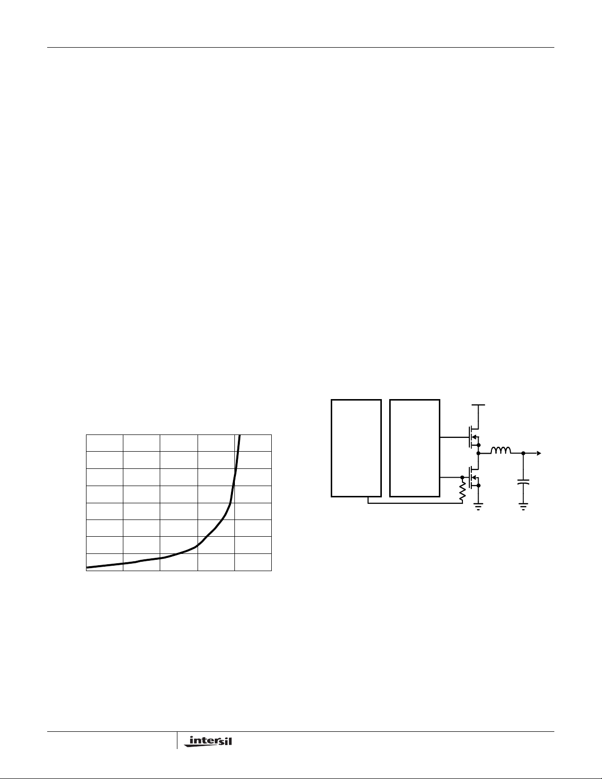
pin to GND will speed up the frequency. See Figure 12 for a
curve that shows the frequency versus resistor value. Note
that the curve is steep as it approaches 300kHz; operation in
this area is not recommended. Since this pin has several
functions muxed onto it, it is important that they do not
interfere with each other. Thus, the circuit that looks for the
resistor will shut off (and default to the 300kHz) if it doesn’t
see a current in the expected range. There should not be any
excessive capacitive loadin g on the pin either , and if a
resistor is used, it should be located very close to the
FS_SYNC pin.
SYNC
With multiple switching regulators running on the same
board at similar, but independent frequencies, there may be
interference between them; a “beat” frequency can develop,
based on the difference between the two frequencies. To
avoid this situation, the ISL6534 has a synchronization
circuit that will read an external frequency, and make the
ISL6534 follow it. The typical circuit involves taking the LG
(Lower Gate) signal from another regulator, going through a
series 10kΩ resistor (to limit the current), and connecting to
the FS_SYNC pin (with no other resistors attached). Within a
few internal clock cycles, the ISL6534 will lock-in to the new
frequency, and run normally as if it were programmed to run
there. If the signal is lost for any reason, after a set number
of clock cycles, the ISL6534 will go back to its default internal
frequency. Note: Do not use the oscillator of another
regulator directly, since the ISL6534 will scale it up by 4 to
match its own internal oscillator; using the LGATE signal will
allow the ISL6534 to match its LGATE to the same
frequency. See Figure 13.
Note that the SYNC circuit expects to see a stable frequency,
and can be fooled by variations. For example, if the gate
signal used has both leading and falling edge modulation, or
an extreme duty cycle, that might cause some confusion.
Skipping clock cycles completely may also be misinterpreted
as a much longer period. The SYNC circuit was designed to
work over a range of 350kHz to 850kHz.
ISL6534
OTHER
REGULAT OR
VIN1
400
350
300
250
)
Ω
200
R (k
150
100
50
0
1 1.5 2 2.5 3 3.5
PERIOD (µs)
FIGURE 12. TYPICAL CLOCK PERIOD vs FS_SYNC
RESISTOR TO GND
UGATE1
LGAT E1
FS_SYNC
FIGURE 13. CONNECTION OF FS_SYNC TO THE LGATE OF
ANOTHER SWITCHING REGULATOR
RFS
VOUT1
Application Considerations
Decoupling Capacitors
Both the VCC12 and VCC pins should have a decoupling
ceramic capacitor (typical values are 1 - 10µF), located as
near to the pin as possible, and with the GND connection as
a via to a wide GND plane. A low-value resistor in series with
the capacitor may help isolate the switching noise from the
power supply from affecting the capacitor, especially if either
pin is sharing a power supply with other noisy circuits (but
adding a resistor in series with the shunt regulator resistor
gives no advantage).
15
FN9134.1
Page 16
ISL6534
SS_EN Capacitors
The basic formula for the soft-start is:
dV
-------
tC
•=
I
where
t is the soft-start ramp time
C is the external capacitor to GND on the SS pin
dV is the voltage the ramp charges up to
(nominal value is 3.3V)
I is the charging current (nominal 30µA).
Or:
time (in ms) = 110 * C (in µF).
Plugging in the known values, and adjusting units, time (in
ms) = 110 * C (in µF). So, for e xample, a 0.1µF capacitor will
give a ramp time of 11ms, and a 1.0µF capacitor will give a
ramp time of 110ms, which is around the practical maximum
value allowed, before noise and leakage and other factors
start changing the formula. Faster ramps are allowed, as
long as the input supplies are capable of charging the output
capacitors (and possibly the load currents, if present at
power-up), without drooping too much (for example, if either
the 5V or 12V supply is dragged down below its POR falling
trip point, because of output loading, that might imply that
the output ramp is too fast (or perhaps bigger input
capacitors are needed, or possibly other explanations as
well).
Note that the above formula determines how long the SoftStart ramp time is. But since the outputs don’t turn on until
the SS/EN pin reaches ~1V, that means the actual time the
output ramps is only ~70% of the total SS ramp.
Note that each of the three regulators can have its own
independent ramp rate, as well as their own independent
enable function (pulling one of the SS_EN pins below 1V
nominal will shut down that output). T w o or three pins can be
tied together to share a common ramp and enable; but note
that there are now two or three times the current charging a
single cap, so the formula should be adjusted accordingly. If
you need the same ramp rate, but separate enable functions,
then don’t share the capacitor; just use the same value
capacitor on each, which will still allow independent
enabling. If you need different ramp rates, but w ant to share
a single enable signal, you will probably need to connect a
separate pull-down FET to each pin, and just drive their
gates from a common signal, or use diodes to isolate a
single FET to multiple pins (as previously shown in Figures 7
and 8).
VREF/REFOUT Capacitors
The VREF output may require a small capacitor to GND to
remain stable; 1.0µF is recommended. If the output is not
used (for example, in DDR mode, where if VOUT1 is divided
down for REFIN); it could be left open, but the additional
noise and current draw may be objectionable. So even then,
a capacitor is recommended.
The REFOUT output is similar; a 0.1µF capacitor is
recommended. If the output is not used, it could be left open,
but the additional noise and current draw may be
objectionable. So even then, a capacitor is recommended.
Linear (VOUT3) Component Selection
Once the VIN3 and VOUT3 levels are defined, the NFET is
chosen to handle the output load current and the power
dissipation it creates. The power is determined by:
Power VIN3 VOUT3–()ILOAD•=
Even if the FET is in a good thermal package (such as a
D-PAK), the mounting of the FET will determine how much
power dissipation is allowed. If simply placed on a pad on an
FR4 board, the dissipation will be limited by the area of the
pad; the more area, the lower the temperature will be. The
recommendation is to use large plane areas, as well as
thermal vias to the back of the board, plus additional area
there, if possible. Even then, power dissipation is usually
limited to 1W or so, which would give 1A (assuming a 1V
drop from VIN3 to VOUT3). See Figure 14.
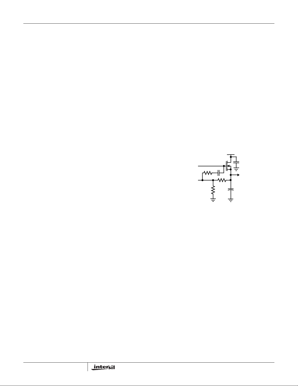
VIN3
DRIVE3
FB3
FIGURE 14. LINEAR (VOUT3) REGULATOR COMPONENT
SELECTION
The output capacitor C
R3
C3
R1
R2
should be chosen for output
OUT3
filtering and transient response needs. However, the output
capacitor also affects the stability of the regulator, so the
choice is limited to a range of acceptable values, which
include the capacitance and its ESR (Effective Series
Resistance).
The input capacitance C
is chosen to keep the input
IN3
supply from changing too much when the output current load
changes; this is related to transient response.
The resistor ratio is chosen to divide the desired output
voltage down to make the FB3 pin = 0.6V. A typical value of
1kΩ for the combined resistance is a good starting value.
The full equation is VOUT3*(R2/(R1+R2) = FB3 = 0.6V.
Compensation components R3 and C3 are chosen to make
the output stable under the conditions being used. Choose
the values to add a zero around 30kHz to cancel a pole.
Values of 4.75K and 6800pF are a good starting point.
NOTE: If the Linear output is not used, leave SS/EN3 open (or tie to
SS1 or SS2); and tie DRIVE3 to FB3, with no other components; this
should disable VOUT3, but keep PGOOD active for VOUT1 and
VOUT2.
CIN3
VOUT3
COUT3
16
FN9134.1
Page 17
ISL6534
Connecting One Input from Another Output
Often, one of the 3 outputs generated is used as the input
voltage to a 2nd (and perhaps 3rd); the general case
includes input or outputs of other IC regulators as well. This
can be done, with a few precautions in mind.
1. The first output must be designed and sized for its own
load current, plus the expected input current of the other
channels.
2. The sequencing of the outputs must be consistent. The
first output cannot be disabled or have a much slower
SS/EN ramp than the input channel, in order to take full
advantage of the soft-start. If the VIN is not present when
the 2nd regulator tries to start up, that can be interpreted
as a short-circuit, and the whole IC could be shut down.
3. The output capacitor of the first is now also the input
capacitor of the 2nd, so it needs to be chosen and sized
for both conditions. For example, transients on the first
output show up on the input of the 2nd; and input current
transients on the 2nd can affect the output of the first.
There may also be trade-offs of the placement of the
various capacitors; some might be near the output FETs
of the first, and some near the input FETs of the 2nd.
4. The linear regulator has no short-circuit protection.
However, if VIN3 is connected to one of the switcher
outputs, a short on the linear output may be detected; but
it is subject to all the cautions mentioned in the SHORTCIRCUIT PROTECTION section.
The modulator transfer function is the small-signal transfer
function of Vout/V
Gain and the output filter (L
break frequency at F
the modulator is simply the input voltage (V
peak-to-peak oscillator voltage ∆V
OSC
COMPARATOR
∆V
OSC
. This function is dominated by a DC
E/A
LC
PWM
-
+
Z
FB
V
E/A
-
+
ERROR
AMP
DETAILED COMPENSATION COMPONENTS
C1
and CO), with a double pole
O
and a zero at F
OSC
DRIVER
DRIVER
Z
IN
REFERENCE
Z
C2
FB
R2
. The DC Gain of
ESR
IN
.
V
IN
L
PHASE
(PARASITIC)
Z
IN
C3
) divided by the
O
ESR
R3
V
OUT
C
O
V
OUT
Feedback Compensation
The compensation required for VOUT1 and VO UT2 is similar
to many other switching regulators, and the same tools can
be used to determine their component values. Note that
VOUT1 and VOUT2 are similar with respect to the
compensation; the only difference is their reference voltages
(fixed 0.6V versus REFIN, which does not directly affect the
component values). The schematics show type 3
compensation, but the simpler type 2 is also possible, under
the right conditions. It is recommended to have footprints for
the T ype 3, in case it is e ver needed; the type 2 is a subset of
that. A simple rule of thumb is that when bulk capacitors are
used on the outputs, the ESR is often high enough (10’s 100mΩ) to use Type 2 compensation. But if only ceramic
capacitors (ESR ~ 1’s mΩ) are used on the outputs, then
most likely Type 3 will be required. Note that the component
labels match the equations given in this section, but may not
match other diagrams in this datasheet.
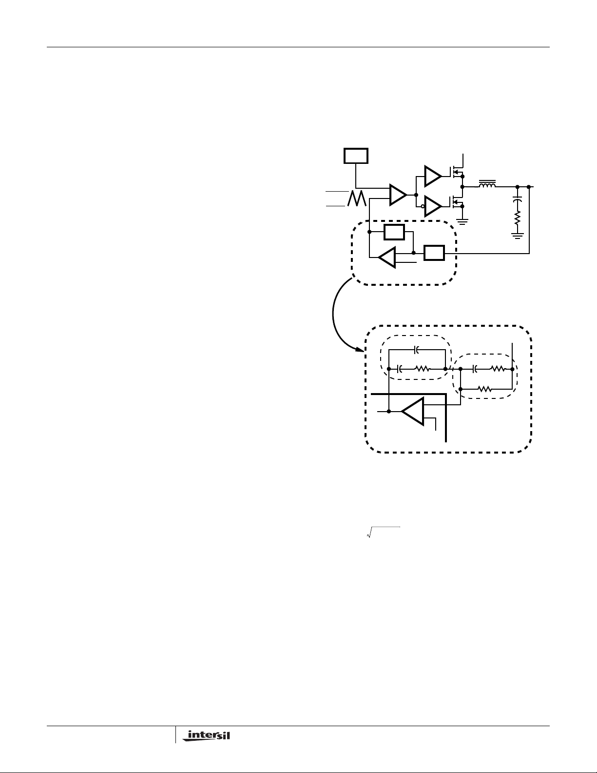
Figure 15 highlights the voltage-mode control loop for a
synchronous-rectified buck converter. The output voltage
(Vout) is regulated to the Reference voltage level. The error
amplifier (Error Amp) output (V
oscillator (OSC) triangular wave to provide a pulse-width
modulated (PWM) wa ve with an amplitude of V
PHASE node. The PWM wav e is smoothed by the output filter
(L
and CO).
O
) is compared with the
E/A
IN
at the
COMP
-
+
ISL6534
FIGURE 15. VOL T A GE-MODE BUCK CONVERTER
COMPENSATION DESIGN
FB
REF
R1
MODULATOR BREAK FREQUENCY EQUATIONS
-------------------------------------- -=
2π L
1
••
OCO
F
ESR
F
LC
1
---------------------------------------------=
2π ESR C
•()•
O
The compensation network consists of the error amplifier
(internal to the ISL6534) and the impedance networks Z
and Z
. The goal of the compensation network is to provide
FB
IN
a closed loop transfer function with the highest 0dB crossing
frequency (f
is the difference between the closed loop phase at f
o
180
. The equations below relate the compensation
) and adequate phase margin. Phase margin
0dB
0dB
and
network’s poles, zeros and gain to the components (R1, R2,
R3, C1, C2, and C3) in Figure 15. Note again that the
component names from Figure 15 apply to the equations
below; they may be labeled with different names elsewhere
in this document. Use these guidelines for locating the poles
and zeros of the compensation network:
17
FN9134.1
Page 18
ISL6534
COMPENSATION BREAK FREQUENCY EQUATIONS
F
Z1
F
Z2
1
----------------------------------=
2π R• 2C1•
------------------------------------------------------=
2π R1 R3+()C3••
-------------------------------------------------------=
F
P1
2π R2•
1
F
P2
----------------------------------
=
2π R3 C3••
1
C1 C2•
----------------------
•
C1 C2+
1
1. Pick Gain (R2/R1) for desired converter bandwidth
2. Place 1ST Zero Below Filter’s Double Pole
(~75% F
3. Place 2
4. Place 1
)
LC
ND
Zero at Filter’s Double Pole
ST
Pole at the ESR Zero
5. Place 2ND Pole at Half the Switching Fr equency
6. Check Gain against Error Amplifier’s Open-Loop Gain
7. Estimate Phase Margin - Repeat if Necessary
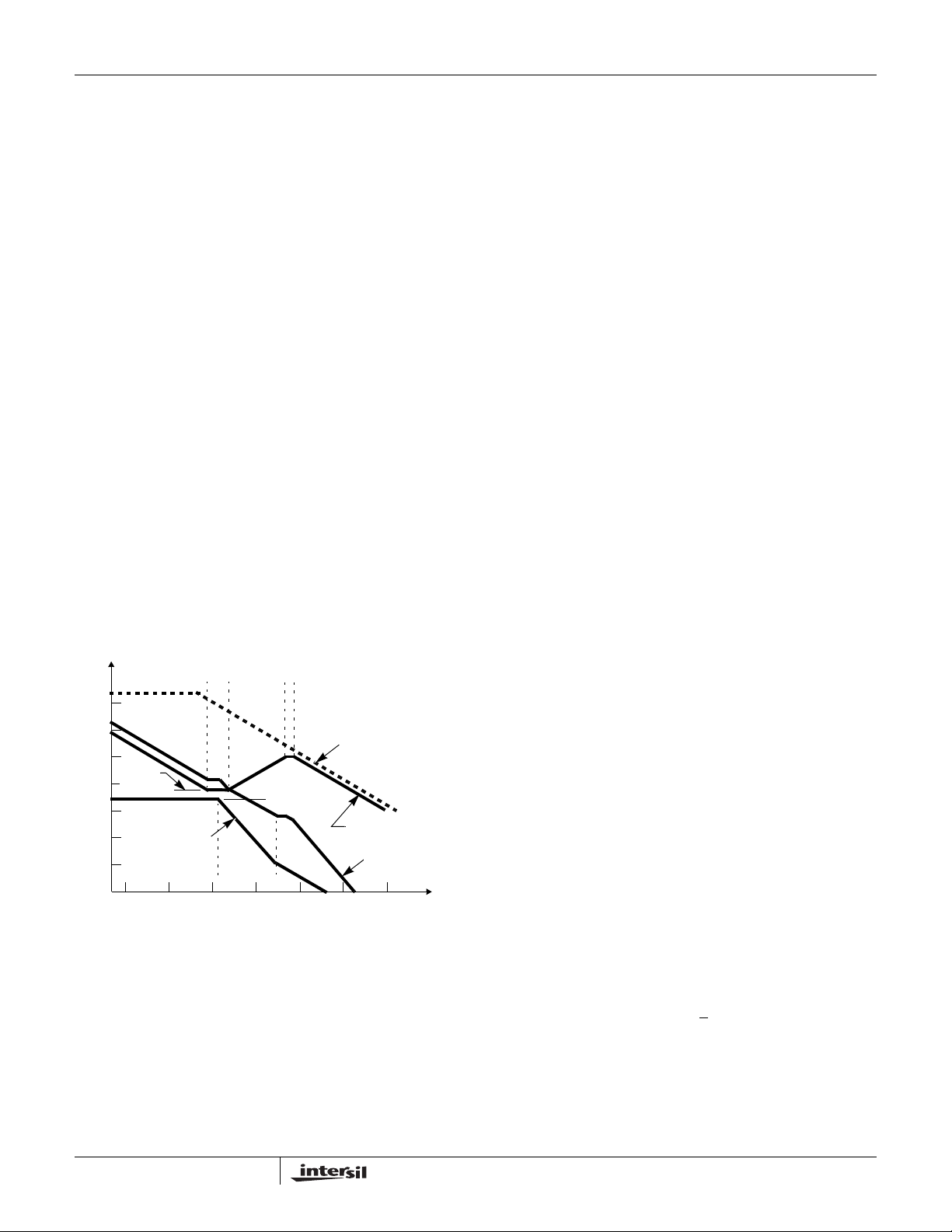
Figure 16 shows an asymptotic plot of the DC-DC
converter’s gain vs. frequency. The actual Modulator Gain
has a high gain peak do to the high Q factor of the output
filter and is not shown in Figure 16. Using the above
guidelines should give a Compensation Gain similar to the
curve plotted. The open loop error amplifier gain bounds the
compensation gain. Check the compensation gain at F
P2
with the capabilities of the error amplifier. The Closed Loop
Gain is constructed on the log-log graph of Figure 16 by
adding the Modulator Gain (in dB) to the Compensation Gain
(in dB). This is equivalent to multiplying the modulator
transfer function to the compensation transfer function and
plotting the gain.
100
80
60
40
20LOG
(R2/R1)
20
GAIN (dB)
0
-20
-40
-60
FIGURE 16. ASYMPTOTIC BODE PLOT OF CONVERTER
MODULATOR
GAIN
GAIN
F
F
Z1
F
P1
Z2
F
LC
F
FREQUENCY (Hz)
(V
ESR
F
P2
20LOG
/∆V
IN
OPEN LOOP
ERROR AMP GAIN
)
OSC
COMPENSATION
GAIN
CLOSED LOOP
GAIN
10M1M100K10K1K10010
The compensation gain uses external impedance networks
Z
and ZIN to provide a stable, high bandwidth (BW) overall
FB
loop. A stable control loop has a gain crossing with 20dB/decade slope and a phase margin greater than 45
o
.
Include worst case component variations when determining
phase margin.
FET Selection (VOUT1, VOUT2)
The typical FET expected to be used will have a low r
(5-10mΩ) and a low Vgs (Gate-to-source threshold voltage;
1-2V). It can be packaged in a thermally enhanced SO-8 IC
package (where the drain leads are thermally connected to
the leadframe under the die, or similar approaches), or even
in more conventional power packages (D-PAK). If the FETs
are surface mounted to the PCB, with only the area of the
power planes to conduct the heat away, then the maximum
load current will be limited by the thermal ratings under those
conditions. Using conventional heatsinks or sufficient airflow
can extend the limit of dissipation.
FETs can be paralleled for higher currents; this spreads the
heat between the FETs, which helps keep the temperature
lower. However, the gate dr iver is now driving twice the gate
capacitance, so there will be more dissipation in the ISL6534
gate drivers.
Typical values for maximum current (based on 8-pin SOIC
FETs surface-mounted on PCB, with no heatsinks or airflow)
are 5A for a dual FET; 10A for single FETs for upper and
lower; and 20A for two FETs in parallel for both upper and
lower. These are just rough numbers; many factors affect it,
such as PCB board area available for heatsinking planes,
how close other dissipative devices are, etc.
In general (and especially for short UGA TE duty cycles, such
as converting 12V input down to 1V or 2V outputs), the
upper FET should be chosen to minimize the Gate charge,
since switching losses dominate. Since the lower FET is on
most of the time, low r
should be the main
DS(ON)
consideration.
The ISL6534 requires 2 N-Channel power MOSFETs for
each switcher output. These should be selected based upon
r
, gate supply requirements, and thermal
DS(ON)
management requirements. The following are some
additional guidelines.
In high-current applications, the MOSFET power dissipation,
package selection and heatsink are the dominant design
factors. The power dissipation includes two loss
components; conduction loss and switching loss. The
conduction losses are the largest component of power
dissipation for both the upper and the lower MOSFETs.
These losses are distributed between the two MOSFETs
according to duty factor (see the equations below). Only the
upper MOSFET has switching losses, since the FET body
diode (or optional external Schottky rectifier) clamps the
switching node before the synchronous rectifier turns on.
P
UPPER
P
LOWER
= I
= I
2
x r
O
DS(ON)
2
x r
O
DS(ON)
Where: D is the duty cycle = V
x D +
x (1 - D)
O/VIN
1
Io x VIN x tSW x Fs
2
,
DS(ON)
tSW is the switching interval, and
Fs is the switching frequency.
18
FN9134.1
Page 19
ISL6534
These equations assume linear voltage-current transitions
and do not adequately model power loss due the reverserecovery of the lower MOSFETs body diode. The
gate-charge losses are dissipated by the ISL6534 and don't
heat the MOSFETs. However, large gate-charge increases
the switching interval, t
which increases the upper
SW
MOSFET switching losses. Ensure that both MOSFETs are
within their maximum junction temperature at high ambient
temperature by calculating the temperature rise according to
package thermal-resistance specifications. A separate
heatsink may be necessary depending upon MOSFET
power, package type, ambient temperature and air flow.
Standard-gate MOSFETs (typically 30V breakdown and 20V
maximum gate voltage) are normally recommended for use
with the ISL6534, especially since 12V is expected to be
available to drive the gates. However, logic-level gate
MOSFETs can be used under special circumstances. The
input voltage, upper gate drive level, and the MOSFETs
absolute gate-to-source voltage rating determine whether
logic-level MOSFETs are appropriate.
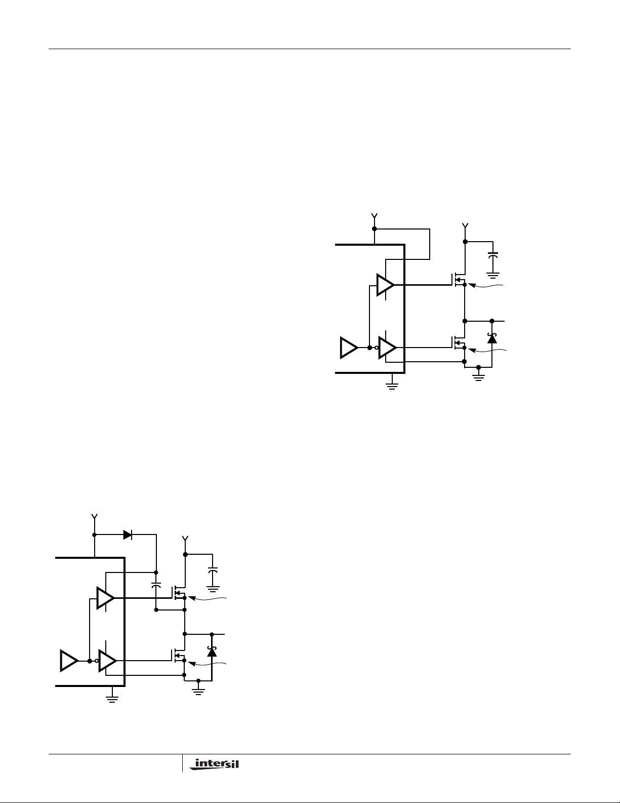
Figure 17 shows the upper gate drive (BOOT pin) supplied
by a bootstrap circuit from VCC12. The boot capacitor,
C
develops a floating supply voltage referenced to the
BOOT
PHASE node. This supply is refreshed each cycle to a
voltage of VCC12 less the boot diode drop (V
) when the
D
lower MOSFET, Q2 turns on. A logic-level MOSFET can only
be used for Q1 if the MOSFETs absolute gate-to-source
voltage rating exceeds the maximum voltage applied to VIN
= VCC12. Note that a lower voltage supply (such as 5V) can
also be used for bootstrapping, which would allow for a lower
gate voltage rating; but only if the lower voltag e is still high
enough to turn the upper FET on hard enough. For Q2, a
logic-level MOSFET can be used if its absolute gate-tosource voltage rating exceeds the maximum voltage applied
to VCC12.
+12V
VCC12
ISL6534
(CHANNEL
1 OR 2)
-
+
FIGURE 17. UPPER GATE DRIVE - BOOTSTRAP OPTION
PGND
VCC12
D
+
GND
BOOT
V
D
BOOT
UGATE
LGATE
PGND
-
PHASE
C
BOOT
+5V OR +12V
Q1
Q2
D2 (OPTIONAL)
NOTE:
V
G-S
NOTE:
V
G-S
≈ V
CC12
≈ VCC12
- V
D
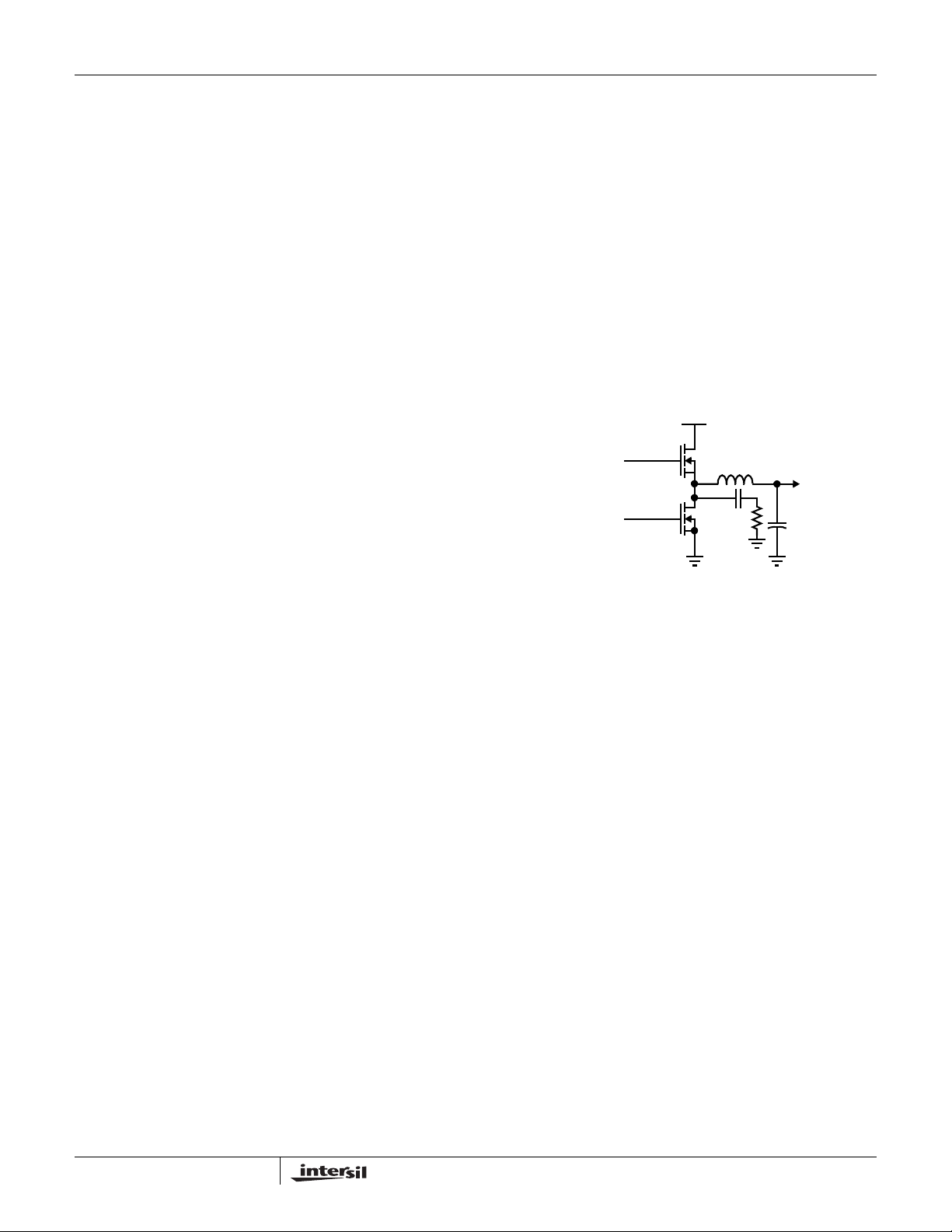
Figure 18 shows the upper gate drive supplied by a direct
connection to VCC12. This option should only be used in
converter systems where the main input voltage is +5 VDC
or less. The peak upper gate-to-source voltage is
approximately VCC12 less the input supply. For +5V main
power and +12 VDC for the VIN bias, the gate-to-source
voltage of Q1 is 7V. A logic-level MOSFET may be a good
choice for Q1 (again, check the max gate voltage ratings)
and a logic-level MOSFET can be used for Q2 if its absolute
gate-to-source voltage rating exceeds the maximum voltage
applied to VCC12.
+12V
VCC12
ISL6534
(CHANNEL
1 OR 2)
-
+
FIGURE 18. UPPER GATE DRIVE - DIRECT VCC12 DRIVE
PGND
VCC12
BOOT
UGATE
PHASE
LGATE
PGND
GND
OPTION
+5V OR LESS
Q1
D2 (OPTIONAL)
Q2
NOTE:
V
G-S
NOTE:
V
G-S
≈ V
CC12
≈ VCC12
- 5V
Bootstrap Trade-offs
Note again that bootstrapping to 12V requires that the upper
FET have a maximum gate-source rating of greater than
12V. Since the LGATE output is sourced from the VCC12
supply in all cases, the lower FET must also have the high
rating. So this may rule out using some 20V breakdown
FETs that have gate ratings of 12V or less.
Figure 17 shows the diode D
C
. A small capacitor (~1µF; not shown) is sometimes
BOOT
used as a local decoupling cap; it should be placed near the
anode of the diode to GND.
The anode of the diode is shown tied to VCC12, but it can
also connect to VCC (even in the shunt regulator mode) or to
VIN or to another appropriate supply.
Figure 18 shows the direct hookup; the advantage is that two
components (D
BOOT
and C
possible disadvantage is that the VCC12 may not be the
optimum voltage for efficiency (perhaps a bootstrap
diode/capacitor to 5V would be better, for example). Once
again, a small capacitor (not shown) located near the
BOOT1 pin is sometimes used for decoupling.
and bootstrap capacitor
BOOT
) are not needed; a
BOOT
19
FN9134.1
Page 20

ISL6534
Note that the PHASE node is not brought into the ISL6534,
so there is no way to reference the gate voltage to it, as is
often done in other regulators. The considerations for the
BOOT2 pin are id entical to BO OT1; but since they may hav e
different VIN, VOUT, FETs, etc., the preferred solution for
each output may be different for any given system.
The voltage required on V
diode anode) depends primarily on the upper NFET r
and Vth. A high voltage makes the r
(Bootstrap Voltage; the
BOOT
DS(ON)
as low as
DS(ON)
possible, which should help the overall efficiency; however,
the high voltage makes the switching power in the gate driver
higher, which lowers the efficiency. So the net overall effect is
a trade-off between the two. At the other extreme, the
voltage must be at least as high as the FET threshold
voltage, plus a few volts of overdrive, in order to turn on the
NFET hard enough to source the maximum load current. So
the r
is not as low, hurting the efficiency, but the gate
DS(ON)
driver power is lower, which help s the efficiency.
Since the gate driver power is a function of (voltage)
theoretical optimum V
voltage is to make it only high
BOOT
2
, the
enough to turn on the NFET to handle the maximum load.
However, since there are usually onl y a few available power
supplies to choose from, the user often must compromise.
And sometimes the only supply available is the same one
used for VIN, which may be good for one term, but not as
good for the other.
The size of the bootstrap capacitor can be chosen by using
the following equations:
Q
GATE
C
BOOT
--------------------
≥ Q
∆V
and
GATE
NQGVIN••
-----------------------------------=
V
GS
where
N is the number of upper FETs
QG is the total gate charge per upper FET
VIN is the input voltage
V
is the gate-source voltage (usually VIN - diode drop)
GS
∆V is the change in boot voltage before and immediately
after the transfer of charge; typically 0.7V to 1.0V
GATE
∆V
NQ
-----------------------------------
G
V
GS
is 11V, ∆V
GS
VIN••
∆V•
13312••
--------------------------- -
11 0.7•
= 1V. In this example,
max
0.051µ F===≥
is
G
Q
C
BOOT
--------------------
The last equation plugs in some typical values: N = 1; Q
33nC, VIN is 12V, V
C
≥ 0.051µF. This value is often rounded up to 0.1µF
BOOT
as a starting value. Note that bootstrap capacitors usually
need to be rated at 16V, to handle the typical 12V boot.
Note that in general, as the number of FETs or the size of
the FETs increases (which usually makes Q
larger) or if
G
VIN or the bootstrap supply (if not VIN) increases (for
example, from 5V to 12V), these all require that C
BOOT
become larger.
Output Inductor Selection
The output inductor is selected to meet the output voltage
ripple requirements and minimize the converter’s response
time to the load transient. The inductor value determines the
converter’s ripple current and the ripple voltage is a function
of the ripple current. The ripple voltage and current are
approximated by the following equations:
∆I =
V
- V
IN
OUT
--------------------------------
Fs x L
V
--------------- -
•
OUT
V
IN
∆V
OUT
= ∆I x ESR
Increasing the value of inductance reduces the ripple current
and voltage. However, the large inductance values reduce
the converter’s response time to a load transient (and usually
increases the DCR of the inductor, which decreases the
efficiency). Increasing the switching frequency (Fs) for a
given inductor also reduces the ripple current and voltage.
One of the parameters limiting the converter’s response to a
load transient is the time required to change the inductor
current. Given a sufficiently fast control loop design, the
ISL6534 will provide either 0% or 87.5% duty cycle in
response to a load transient. The response time is the time
required to slew the inductor current from an initial current
value to the transient current level. During this interval the
difference between the inductor current and the transient
current level must be supplied by the output capacitor.
Minimizing the response time can minimize the output
capacitance required.
The response time to a transient is different for the
application of load and the removal of load. The following
equations give the approximate response time interval for
application and removal of a transient load:
LOI
LOI
×
TRAN
RISE
where: I
------------------------------- -=
–
V
INVOUT
is the transient load current step, t
TRAN
t
FALL
response time to the application of load, and t
×
TRAN
-------------------------------=t
V
OUT
is the
RISE
is the
FALL
response time to the removal of load. With a +5V input
source, the worst case response time can be either at the
application or removal of load and dependent upon the
output voltage setting. Be sure to check both of these
equations at the minimum and maximum output levels f or the
worst case response time.
Output Capacitors Selection
An output capacitor is required to filter the output and supply
the load transient current. The filtering requirements are a
function of the switching frequency and the ripple current.
The load transient requirements are a function of the slew
rate (di/dt) and the magnitude of the transient load current.
These requirements are generally met with a mix of
capacitors and careful layout.
Modern microprocessors produce transient load rates above
1A/ns. High frequency capacitors initially supply the transient
20
FN9134.1
Page 21
ISL6534
and slow the current load rate seen by the bulk capacitors.
The bulk filter capacitor values are generally determined by
the ESR (effective series resistance) and voltage rating
requirements rather than actual capacitance requirements.
High frequency decoupling capacitors should be placed as
close to the power pins of the load as physically possible. Be
careful not to add inductance in the circuit board wiring that
could cancel the usefulness of these low inductance
components. Consult with th e man ufacturer of the load on
specific decoupling requirements. And keep in mind that not all
applications have the same requirements; some may need
many ceramic capacitors in parallel; others may need only one.
Use only specialized low-ESR capacitors intended for
switching-regulator applicatio ns for the b ulk capacitors. The
bulk capacitor’s ESR will deter mine the output r ipple
voltage and the initial voltage drop after a high slew-rate
transient. An aluminum electrolytic capacitor's ESR v alue is
related to the case size with lower ESR available in larger
case sizes. However, the equivalent series inductance
(ESL) of these capacitors increases with case size and can
reduce the usefulness of the capacitor to high slew-rate
transient loading. Unfortunately, ESL is not a specified
parameter. Wor k with your capacitor supplier and measure
the capacitor’s impedance with frequency to select a
suitable component. In most cases, multiple electrolytic
capacitors of small case size perform better than a single
large case capacitor.
Input Capacitor Selection
Use a mix of input bypass capacitors to control the voltage
overshoot across the MOSFETs. Use small ceramic
capacitors for high frequency decoupling and bulk capacitors
to supply the current needed each time Q1 turns on. Place
the small ceramic capacitors physically close to the
MOSFETs and between the drain of Q1 and the source of Q2 .
The important parameters for the bulk input capacitor are the
voltage rating and the RMS current rating. For reliable
operation, select the bulk capacitor with voltage and current
ratings above the maximum input voltage and largest RMS
current required by the circuit. The capacitor voltage rating
should be at least 1.25 times greater than the maximum
input voltage and a voltage rating of 1.5 times is a
conservative guideline. The RMS current rating requirement
for the input capacitor of a buck regulator is approximately
1/2 the DC load current.
For both through-hole and surface-mount design, several
electrolytic capacitors (Panasonic HFQ series or Nichicon
PL series or Sanyo MV-GX or equivalent) may be needed.
For surface mount designs, solid tantalum capacitors can be
used, but caution must be exercised with regard to the
capacitor surge current rating. These capacitors must be
capable of handling the surge-current at power-up. The TPS
series available from AVX, and the 593D series from
Sprague are both surge current tested.
Snubbers
A snubber network is a series resistor and capacitor, usually
from the phase node to GND (across the lower FET); it is
used to dampen the ringing of the phase node, which can
introduce noise into other parts of the ci rcuit. In particular,
jitter on the gate drivers can be caused by disturbances that
trigger the programmable duty cycle edge of the internal
ramp generator. If noise or ringing is a problem in your
particular circuit, consider adding a snubber. Typical values
are 2.2nF for the capacitor, and 2.2Ω for the resistor. Note
that the resistor may have large currents, so use a 1/2W type
resistor. The order of R and C doesn’t usually matter, but one
preference is putting the resistor to GND, such that the
voltage across it can be easily measured on an oscilloscope
to represent the current. See Figure 19.
VIN1
UGATE1
PHASE1
LGATE1
FIGURE 19. SNUBBER COMPONENT SELECTION
CSN1
VOUT1
RSN1
Optional Schottky Selection
An optional rectifier D2 (see Fig 17 or 18) is a clamp that
catches the negative inductor s win g during the dead time
between turning off the lower MOSFET and turning on the
upper MOSFET . The diod e must be a Schottky type to preven t
the lossy parasitic MOSFET body diode from conducting. If
used, connect the cathode to the phase node, and the anode
to PGND . It is acceptab le to omit the dio de and let the body
diode of the lower MOSFET clamp the negative inductor
swing, but efficiency will drop one or two percen t as a result.
The diode's rated rev erse breakdo wn v oltage must be gr eater
than the maximum input voltage .
Margining and “Fine-Tuning”
Margining can be added externally to a voltage regulator, in
order to raise and/or lower the output voltage a nominal
amount, such as ±10%. The purpose might be to run the
processor at higher voltage for faster clock speeds, or to run
at lower voltages, to save power, for example.
A straightforward method involv es adding tw o e xtra resistors
and two small FETs (and re-adjusting R2, depending upon
the decoding used); see Figure 20. Both resistors (RM1,
RM2) are high values (10-100kΩ) compared to R1 and R2
(~1kΩ). So when placed in parallel with R2, it lowers the
resistance of R2; pick the values for the desired amount.
Some simple logic is needed on the gates A and B to control
them; pull-up or pull-down resistors might also be needed.
21
FN9134.1
Page 22
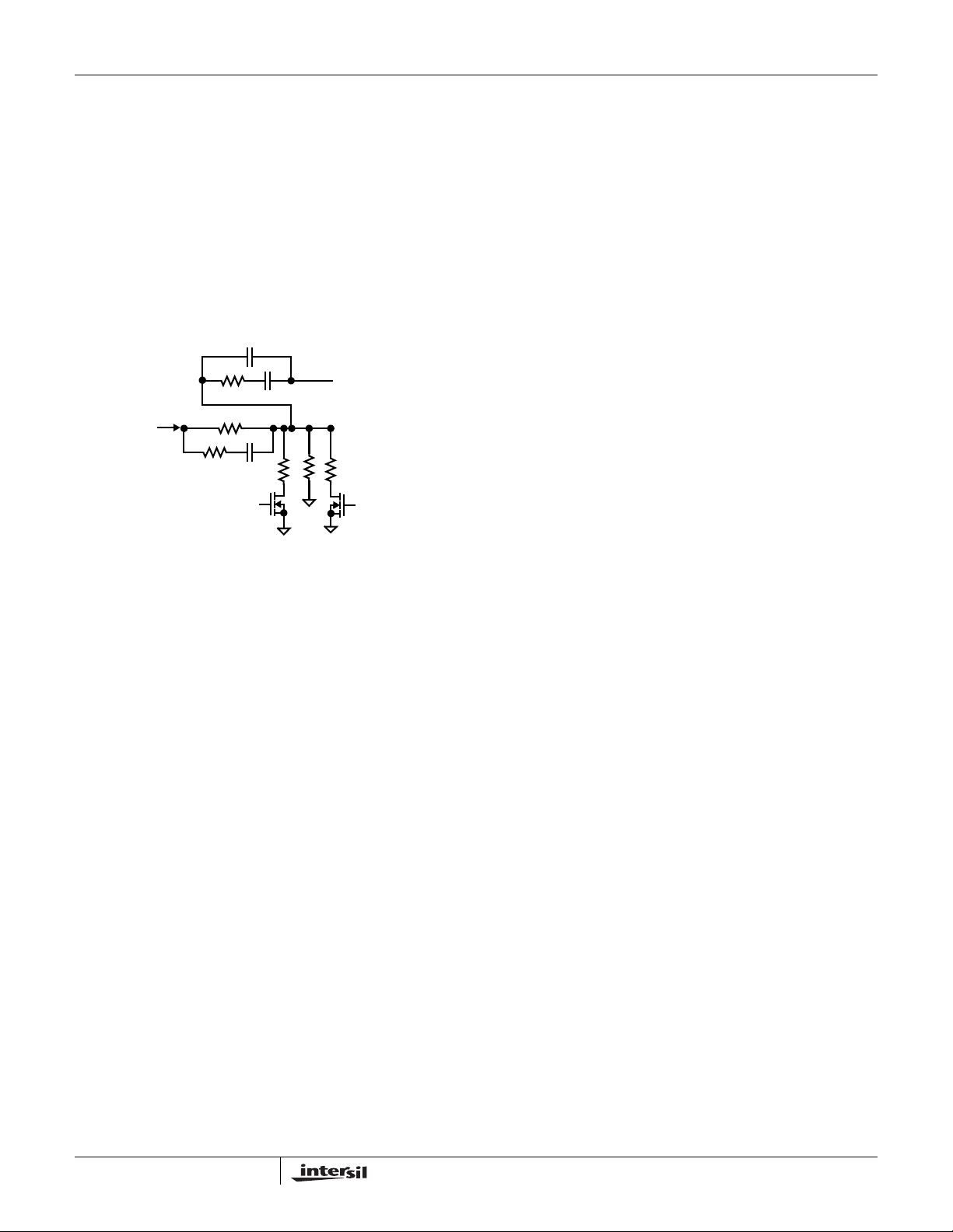
ISL6534
Only 3 of the 4 possible states are shown decoded. There
are other variations of this technique, but this shows the
basic principle. Since the FB are sensitive nodes, care
should be taken in the layout, to keep the e xtra resistors near
the pin.
A variation of this technique can be used without the margining
to fine tune the output voltage, when two 1% resistors (R1, R2)
can’t give the exact value desired, and an active factory trim is
not feasible. Simply use a much higher value resistor in parallel
with either R1 or R2 (or both) to fine-tune the value; a 100-1
ratio in resistor values will be able to change the voltage by
roughly 1%; that might be good enough.
COMP1
VOUT1
RM1, RM2 >> R1, R2
A OFF, B OFF 10% HIGH
A OFF, B ON NOMINAL
A ON, B ON 10% LOW
FIGURE 20. MARGINING COMPONENT SELECTION
R1
FB1
R2
RM1RM2
AB
Short-Circuit Protection
The ISL6534 does not have the typical over-current
protection used by many of the Core Processor IC’s. Instead,
it has a simple and inexpensive method of protection. But it
is important for the user to understand the method used, and
the limitations of that method.
There are no sense pins available on the ISL6534. This
means that the many standard ways of sensing output
current (sense resistors, FET r
are not possible, without adding a lot of external
components. There are also no Phase pins available.
Monitoring Under-Voltage (by sensing drops on the FB pins,
or on the outputs) was not done.
The only method of protection for the two switching
regulators is to monitor the COMP1 and COMP2 pins for
over-voltage (and note that the linear output has no
protection at all). What happens on a short-to-GND on the
output? As the output voltage is dragged down, the FB pin
should start to follow, since it is usually just a resistor divider
from the output. The loop detects that the FB pin is lower
than the Error-Amp reference, and the COMP voltage will
rise to try to equalize them; that will increase the duty-cycle
of the upper FET gate driver (which allows more time to pull
the output voltage higher). If the short is hard enough, the
COMP pin will rise higher and the duty cycle will increase
further. If the short is still too hard, at some point the COMP
pin output will go out of range, the duty cycle will hit the
maximum, and the loop can no longer effectively try any
, Inductor DCR, etc.)
DS(ON)
harder. This is the point at which an Over-Current condition
is detected. A comparator monitors the COMP pins, and if
either one exceeds the trip point (nominal 3.3V), and stays
above it for a filter time (1-2 clock pulses of the internal
oscillator; 3-6µs at the nominal 300kHz; 2-4µs at 500kHz),
then it will shut down both switchers, as well as the linear
regulator, and require a POR on either (or both) of the
VCC12 or VCC power pins. There is no “hiccup” mode,
where it keeps trying.
So that is the detection method; what are the implications of
it? On the plus side, it’s built in, and the user doesn’t have to
set anything to use it; no additional components are
required. On the negative side, it is not easy to predict its
performance, since many factors can affect how well it
works. It was designed to detect a “hard” short; like a
screwdriver shorting the output to GND. But defining how
close to “zero ohms” the short has to be in order to work
properly is not straightforward. If the resistance is too high to
trip the detector, the regulator will react simply as if the load
has increased, and will continue to try to regulate up until the
FETs overheat. If the COMP pin doesn’t immediately rise to
its trip point when the short is applied, chances are it won’t
trip later as the FETs heat up. So most of the potential
problems can occur if the initial trip is missed.
Following are a list of the many possible factors that affect
the performance:
1. If the power supply used for the VIN of one of the
regulators is shared with the VCC12 (or VCC) supply of
the IC, then shorting the output could potentially
momentarily drag down the supply low enough to trip the
VCC12 (or VCC) falling POR, which could result in
unpredictable behavior once the outputs shut off due to
the POR, and then try to start up into the short after the
supply recovers. This scenario can be avoided with a
“stiff” power supply, or a separate one.
2. If the power supply for VIN has a built-in current shutdown
or limit, then it might shut-down before the IC, or the
limiting might help the IC shutdown, either of which is
generally good. However, many supplies used in real
systems don’t have this built in, or would require a much
higher current short than this scenario would provide.
3. If the circuit survives the initial short but doesn’t shut
down, the removal of the short can cause an inductive
kick on the phase node, which can create an over-voltage
condition on the boot pin, which can in the worst case
damage the IC and/or the FETs.
4. The resistance of the short itself is probably the most
critical factor affecting the over-current shutdown
performance. If the short is not low enough resistance,
then the part will NOT shutdown, and the FETs can
overheat. Note that the “short” to the output also includes
wiring, PCB traces, contact resistances, as well as all of
the return paths.
5. The higher the output voltage, the more current you will
get out of a fixed-resistance short, and the more likely you
22
FN9134.1
Page 23
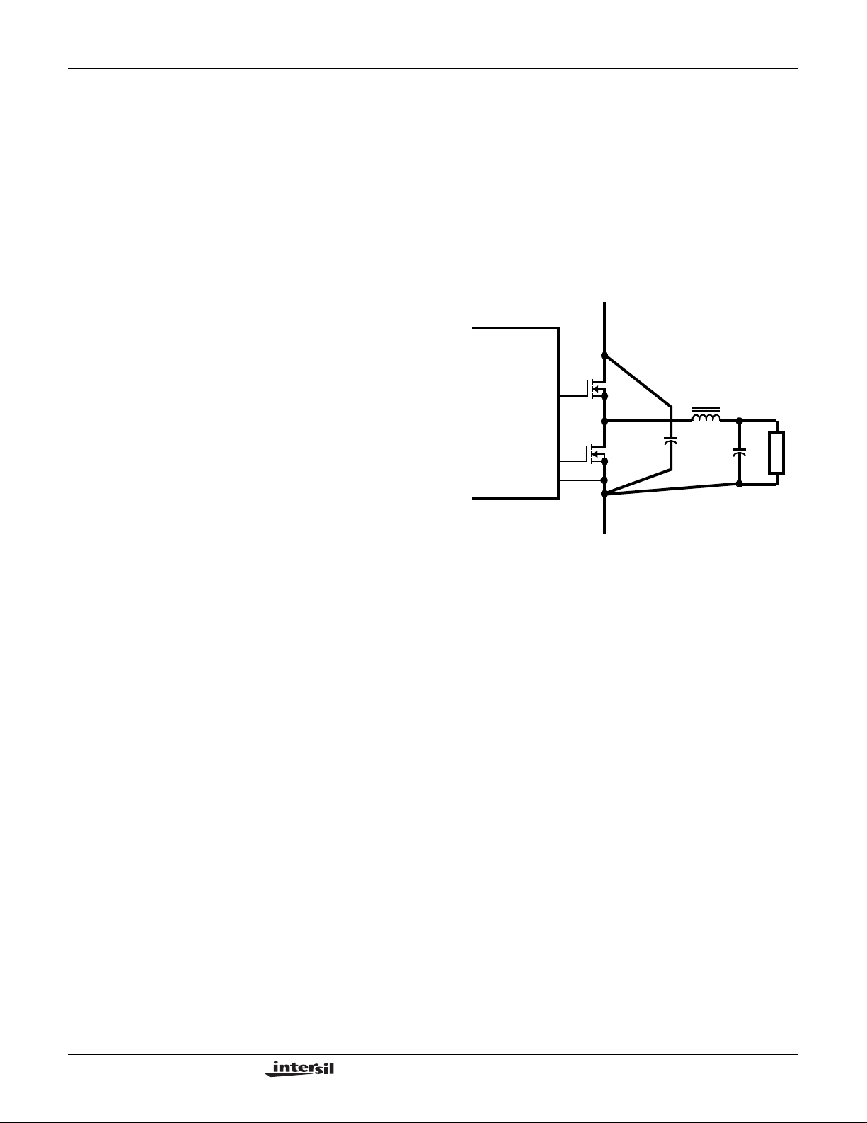
ISL6534
will get a clean shutdown; see also #6. In addition, the
higher VOUT for a given VIN will give a higher UGATE
duty cycle, and the average COMP v oltage is higher, so it
doesn’t have as far to go to trip.
6. In general, the faster the rise time of the output current
during the short, the more current will be allowed on the
initial peak, and the better chance the COMP pin will have
a sharp rise as well. A low resistance short (#4) and a
higher output voltage (#5) both help. However, if the
current ramps too fast, then a false trip is also possible
(shutting down at a current level still within the ex pected
load range).
7. The load current at the time of the short can affect the
results; the response of a short can be different at no load
versus full load.
8. The compensation compone nts are chosen to stabilize
the regulation loop; however, if they unnecessarily load
the COMP output, that could affect the trip point
response.
9. The output capacitance and its ESR can affect how
quickly the current ramps up during a short.
10. Other variables that may contribute to a lesser degree
include variations in the COMP comparator and filter, the
inductor L and DCR, the r
of the FET, the FB
DS(ON)
resistor dividers, the error amp reference voltage, the
oscillator frequency, switching noise, VCC voltage,
ambient temperature and airflow, and the lay out of the
PCB.
11. Adding external circuitry to sense a fault may be possible,
but subject to the usual limitations of those circuits. For
example, sensing the output or FB voltage doesn’t always
directly correlate with output current.
So the recommendations are as follows:
1. If there is a specific fault condition that needs protection,
try it out first under controlled conditions, either on an
EVAL board, the final circuit, or something close to it,
along with the power supply that will also be used.
Monitor VCC12 and VCC (to be sure they aren’t tripping
POR), the output and the COMP pin. A current probe
monitoring the output current is also very useful.
2. Compare the short circuit resistance to the nominal load
resistance; if they are too close, the circuit may not work
well. Calculate how long the FETs can sit at the higher
current. Is the short more likely from zero load or full
load?
3. Check the rise time of the short circuit current, and what
happens if when the short is released.
4. From the waveform of the COMP pin, see if the values
can be optimized for the short condition. Within the
constraints of the stability criteria, smaller caps (in
general) may give a quicker re sponse.
5. Note that the linear output has no protection at all.
PCB Layout Considerations
General Layout Considerations
As in any high frequency switching converter, layout is very
important. Switching current from one power device to
another can generate voltage transients across the
impedances of the interconnecting bond wires and circuit
traces. These interconnecting impedances should be
minimized by using wide, short printed circuit traces. The
critical components should be located as close together as
possible using ground plane construction or single point
grounding.
V
IN
ISL6534
UGATE
LGATE
PGND
FIGURE 21. PRINTED CIRCUIT BOARD POWER AND
GROUND PLANES OR ISLANDS
Figure 21 shows the critical power components of the
converter, for either output channel. To minimize the voltage
overshoot the interconnecting wires indicated by heavy lines
should be part of ground or power plane in a printed circuit
board. The components shown in Figure 21 should be
located as close together as possible. Please note that the
capacitors C
and CO each represent numerous physical
IN
capacitors. Locate the ISL6534 within 1-2 inches (or even
less, if possible) of the MOSFETs, Q1 and Q2. The circuit
traces for the MOSFETs’ gate and source connections from
the ISL6534 must be sized to handle up to 1.5A peak
current.
Figure 22 shows the circuit traces that require additional
layout consideration. Use single point and ground plane
construction for the circuits shown. Minimize any leakage
current paths on each of the SS pins and locate the
capacitors, C
close to the SS pin because the internal
ss
current source is only 30µA. Provide local V
between VCC12 and PGND pins, as well as the VCC and
GND pins. Locate the capacitor, C
to the BOOT pin and PHASE node. Note that the PGND pins
are used only for the gate drivers and other output circuitry
(including the VCC12 decoupling capacitor); the GND pins
are used by the VCC pin, and the control circuitry. They
should be joined at a common point.
Q1
Q2
RETURN
L
O
C
IN
C
CC12
as close as practical
BOOT
V
OUT
O
decoupling
LOAD
23
FN9134.1
Page 24
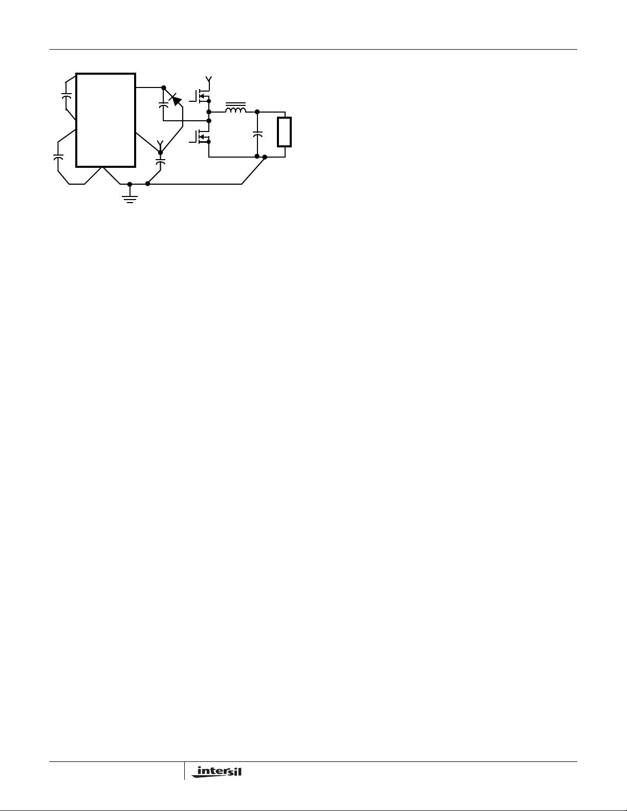
ISL6534
C
VCC
VCC
GND
SS
C
SS
FIGURE 22. PRINTED CIRCUIT BOARD SMALL SIGNAL
BOOT
C
ISL6534
VCC12
GND
PGND
LAYOUT GUIDELINES
BOOT
PHASE
+12V
D1
C
VCC12
Q1
+V
Q2
IN
L
O
V
OUT
C
O
Layout Considerations for the ISL6534
The metal plate on the bottom of either the TSSOP or QFN
(MLFP) package must be soldered down to the PC board,
and sufficient plane area given for heat transfer. The plane
should be connected to GND (pin 15 in TSSOP); but if it is
left floating, it should NOT be tied to any other potential.
Thermal vias are recommended to connect to a plane on the
opposite side of the PCB, and to the internal GND plane, for
additional heat transfer.
Decoupling capacitors should be very close to the VCC12
and VCC5 pins, with vias to the GND plane.
The traces from the gate drivers to the FETs (UG1, UG2,
LG1, LG2, DRIVE3) should be short (for low resistance) and
wide (to handle large currents); the pin spacing will limit the
widths right near the package. But note that the closer the
FETs are to the IC, the more they will heat each other, so
keep that thermal consideration in mind.
BOOT1/2 capacitors should be near their pins; the bottom to
phase and diode can be a little further away. If a separate
small capacitor is used for the bootstrap supply (if different
than either VIN or VCC12), it should be located next to the
bootstrap diode anode.
LOAD
Other traces to keep short include:
• FB1/2/3: the resistor dividers should be near the IC; via to
GND plane; the signal from the VOUT can travel, since it is
low impedance.
• Resistor dividers used for references (from VREF or
VOUT or to REFIN) should be near the REFIN input.
• COMP1/2: the compensation components should be close
to these pins (as well as FB1/2 pins), with vias to the GND
plane.
• EN_SS capacitors should be near pin, with vias to GND
plane.
• FS_SYNC resistor (if needed) should be near pin, with a
via to GND.
• Output capacitors should be close to the loads, where the
filtering will help most; small ceramic capacitors (~1µF) in
parallel help for high frequency transients. Input capacitors
should be near the VIN pins of the FETs; the input
capacitor GNDs should be close to the lower FET GND as
well.
• The VIN plane should be large to heatsink the upper FET
effectively, since the drain pin is usually the thermal node.
By the same reasoning then, the phase node plane should
also be large, since the lower FET drain is connected
there. However, the phase node plane couples high
frequency switching noise to other levels nearby, so it
should be minimized for that reason. And don’t route any
sensitive or high impedance signals over the phase
planes.
Several placement approaches are possible:
• IC and output FETs, caps, and inductors on top level; most
of the miscellaneous resistors and capacitors on the
bottom level;
• All components on top level, with output components
facing pins 13-24 side of IC, and input components facing
pins 1-12.
24
FN9134.1
Page 25
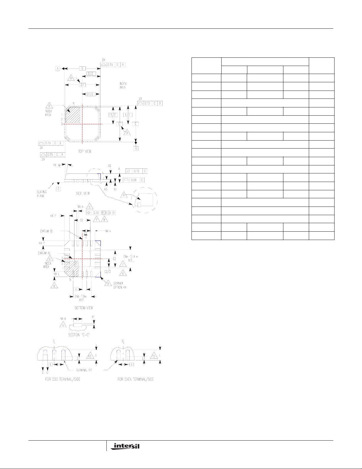
ISL6534
Quad Flat No-Lead Plastic Package (QFN)
Micro Lead Frame Plastic Package (MLFP)
L32.5x5
32 LEAD QUAD FLAT NO-LEAD PLASTIC PACKAGE
(COMPLIANT TO JEDEC MO-220VHHD-2 ISSUE C
MILLIMETERS
SYMBOL
A 0.80 0.90 1.00 A1 - - 0.05 A2 - - 1.00 9
A3 0.20 REF 9
b 0.18 0.23 0.30 5,8
D 5.00 BSC D1 4.75 BSC 9
D2 2.95 3.10 3.25 7,8
E 5.00 BSC E1 4.75 BSC 9
E2 2.95 3.10 3.25 7,8
e 0.50 BSC k0.25 - - L 0.30 0.40 0.50 8
L1 - - 0.15 10
N322
Nd 8 3
Ne 8 8 3
P- -0.609
θ --129
NOTES:
1. Dimensioning and tolerancing conform to ASME Y14.5-1994.
2. N is the number of terminals.
3. Nd and Ne refer to the number of terminals on each D and E.
4. All dimensions are in millimeters. Angles are in degrees.
5. Dimension b applies to the metallized terminal and is measured
between 0.15mm and 0.30mm from the terminal tip.
6. The configuration of the pin #1 identifier is optional, but must be
located within the zone indicated. The pin #1 identifier may be
either a mold or mark feature.
7. Dimensions D2 and E2 are for the exposed pads which provide
improved electrical and thermal performance.
8. Nominal dimensions are provided to assist with PCB Land Pattern
Design efforts, see Intersil Technical Brief TB389.
9. Features and dimensions A2, A3, D1, E1, P & θ are present when
Anvil singulation method is used and not present for saw
singulation.
10. Depending on the method of lead termination at the edge of the
package, a maximum 0.15mm pull back (L1) maybe present. L
minus L1 to be equal to or greater than 0.3mm.
NOTESMIN NOMINAL MAX
Rev. 1 10/02
25
FN9134.1
Page 26
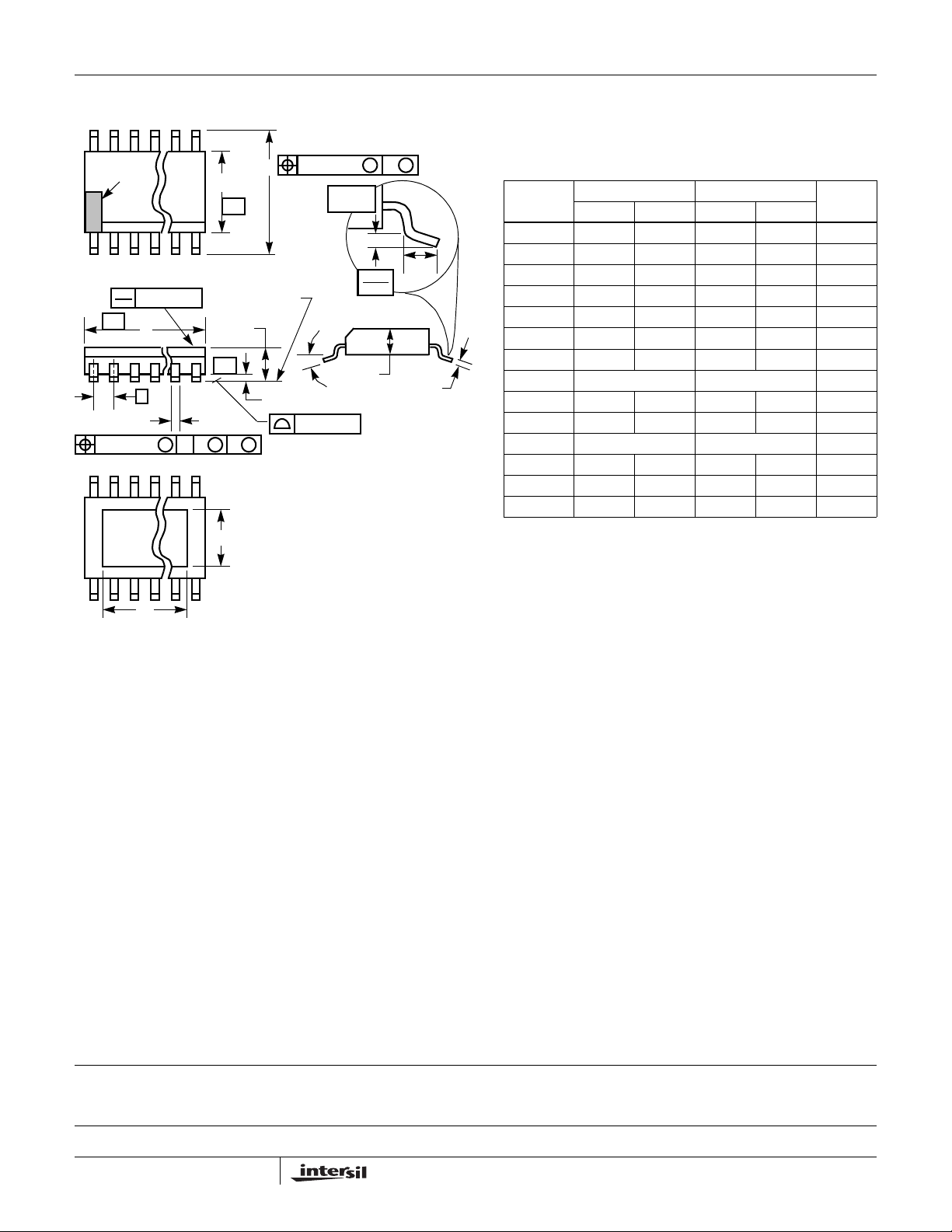
ISL6534
Thin Shrink Small Outline Exposed Pad Plastic Packages (EPTSSOP)
N
INDEX
AREA
123
TOP VIEW
0.05(0.002)
-AD
e
b
0.10(0.004) C AM BS
123
N
P
BOTTOM VIEW
E1
E
-B-
SEA TING PLANE
A
-C-
A1
M
P1
0.25(0.010) BM M
GAUGE
PLANE
0.25
0.010
α
0.10(0.004)
A2
M24.173B
24 LEAD THIN SHRINK SMALL OUTLINE EXPOSED PAD
PLASTIC PACKAGE
INCHES MILLIMETERS
SYMBOL
NOTESMIN MAX MIN MAX
A - 0.047 - 1.20 -
L
A1 0.000 0.006 0.00 0.15 A2 0.031 0.051 0.80 1.05 -
b 0.0075 0.0118 0.19 0.30 9
c 0.0035 0.0079 0.09 0.20 -
D 0.303 0.311 7.70 7.90 3
E1 0.169 0.177 4.30 4.50 4
c
e 0.026 BSC 0.65 BSC E 0.246 0.256 6.25 6.50 L 0.0177 0.0295 0.45 0.75 6
N24 247
o
α
0
o
8
o
0
o
8
-
P - 0.197 - 5.00 11
P1 -0.126-3.2011
Rev. 1 11/03NOTES:
1. These package dimensions are within allowable dimensions of
JEDEC MO-153-ADT, Issue F.
2. Dimensioning and tolerancing per ANSI Y14.5M-1982.
3. Dimension “D” does not include mold flash, protrusions or gate
burrs. Mold flash, protrusion and gate burrs shall not exceed
0.15mm (0.006 inch) per side.
4. Dimension “E1” does not include interlead flash or protrusions.
Interlead flash and protrusions shall not exceed 0.15mm (0.006
inch) per side.
5. The chamfer on the body is optional. If it is not present, a visual
index feature must be located within the crosshatched area.
6. “L” is the length of terminal for soldering to a substrate.
7. “N” is the number of terminal positions.
8. Terminal numbers are shown for reference only.
9. Dimension “b” does not include dambar protrusion. Allowable
dambar protrusion shall be 0.08mm (0.003 inch) total in excess
of “b” dimension at maximum material condition. Minimum space
between protrusion and adjacent lead is 0.07mm (0.0027 inch).
10. Controlling dimension: MILLIMETER. Converted inch dimensions are not necessarily exact. (Angles in degrees)
11. Dimensions “P” and “P1” are thermal and/or electrical enhanced
variations. Values shown are maximum size of exposed pad
within lead count and body size.
All Intersil U.S. products are manufactured, assembled and tested utilizing ISO9000 quality systems.
Intersil Corporation’s quality certifications can be viewed at www.intersil.com/design/quality
Intersil products are sold by description only. Intersil Corporation reserves the right to make changes in circuit design, software and/or specifications at any time without
notice. Accordingly, the reader is cautioned to verify that data sheets are current before placing orders. Information furnished by Intersil is believed to be accurate and
reliable. However, no responsibility is assumed by Intersil or its subsidiaries for its use; nor for any infringements of patents or other rights of third parties which may result
from its use. No license is granted by implication or otherwise under any patent or patent rights of Intersil or its subsidiaries.
For information regarding Intersil Corporation and its products, see www.intersil.com
26
FN9134.1
 Loading...