

Page 1
TM
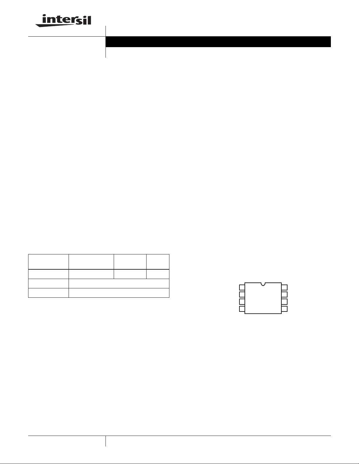
GND
VCC
DRIVE2
FB2
UGATE
FB
COMP
BOOT
8
7
6
5
1
2
3
4
ISL6528
(SOIC)
ISL6528
Data Sheet February 2002
Dual Regulator - Standard Buck PWM
and Linear Power Controller
The ISL6528 provides the power control and protection for
two output voltages in high-performance graphics cards and
other embedded processor applications. The dual-output
controller drives an N-Channel MOSFET in a standard buck
topology and a NPN pass transistor in a linear configuration.
The ISL6528 provides both a regulated high current, low
voltage supply and an independent, lower current supply
integrated in an 8-lead SOIC package. The controller is ideal
for graphics card applications where both graphics
processing unit (GPU) and memory supplies are required.
The standard buck converter is a simple, single feedback
loop, voltage-mode control with fast transient response. Both
the switching regulator and linear regulator provide a
maximum static regulation tolerance of ±2% over line, load,
and temperature ranges. Each output is user-adjustable by
means of external resistors.
An integrated soft-start feature brings both supplies into
regulation in a controlled manner. Each output is monitored
via the FB pins for undervoltage events. If either output
drops below 52.5% of the internal reference voltage, both
regulators are shutdown.
Ordering Information
PKG.
PART NUMBER TEMP. RANGE (oC) PACKAGE
ISL6528CB 0 to 70 8 Ld SOIC M8.15
ISL6528CB-T
ISL6528EVAL1 Evaluation Board
8Ld SOIC Tape and Reel
NO.
FN9038.1
Features
• Provides two regulated voltages
- One standard buck PWM
- One linear controller
• Small converter size
- 600kHz constant frequency operation
- Small external component count
• Excellent output voltage regulation
- Both outputs: ±2% over temperature
• Single 5V bias and bootstrap supply
• Output voltage range: 0.8V to 3.3V
• Simple single-loop voltage-mode PWM control design
• Fast PWM converter transient response
- High-bandwidth error amplifier
- Full 0–100% duty ratio
• Linear controller drives bipolar linear pass transistor
• Fully-adjustable outputs
• Undervoltage fault monitoring on both outputs
Related Literature
•Technical Brief TB363
Processing Moisture Sensitive Surface Mount Devices
(SMDs)
Guidelines for Handling and
Pinout
TOP VIEW
Applications
•
Graphics–GPU and memory supplies
• ASIC power supplies
• Embedded processor and I/O supplies
• DSP supplies
1
CAUTION: These devices are sensitive to electrostatic discharge; follow proper IC Handling Procedures.
1-888-INTERSIL or 321-724-7143
|
Intersil (and design) is a trademark of Intersil Americas Inc.
Copyright © Intersil Americas Inc. 2002, All Rights Reserved
Page 2
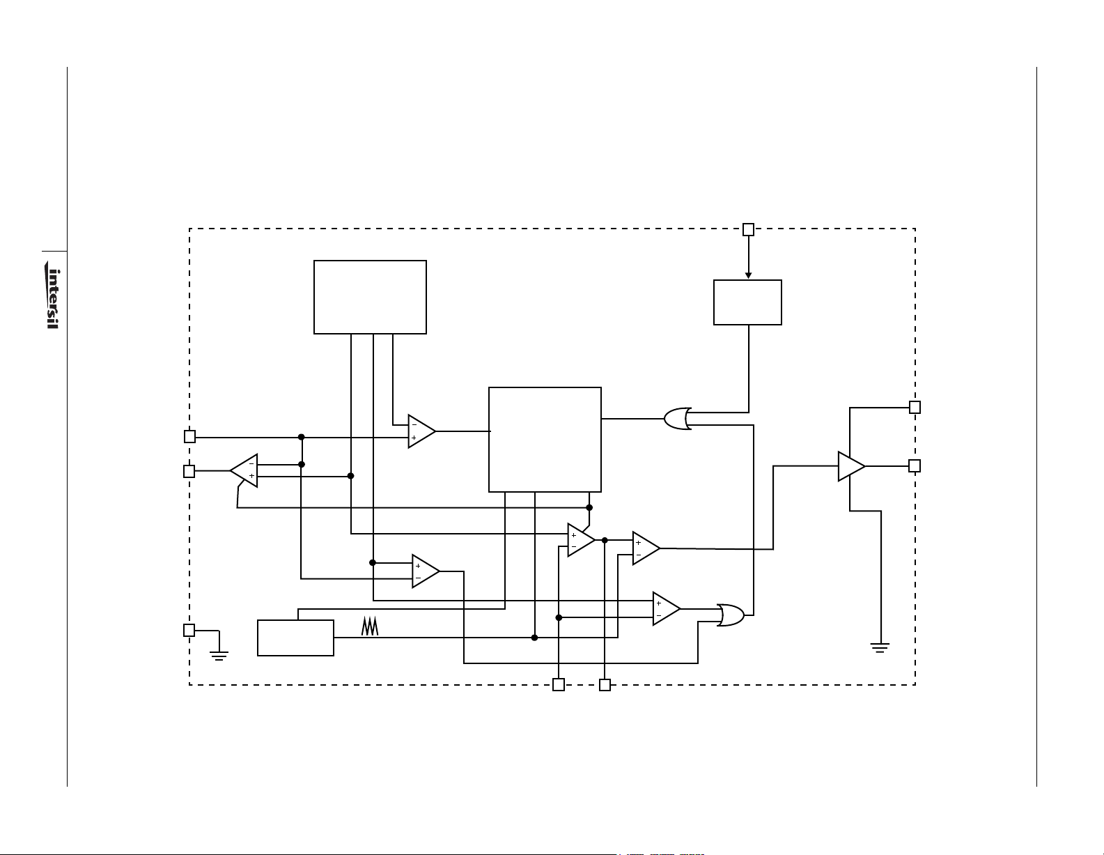
Block Diagram
2
VCC
FB2
DRIVE2
GND
INHIBIT/SOFT-START
EA2
INHIBIT
SOFT-START
OSCILLATOR
VOLTAGE
REFERENCE
0.80V
0.42V
1.28V
SHUTDOWN
UV2
SOFT-
START
AND FAULT
LOGIC
EA1
RESTART
INHIBIT
SOFT-START
COMP1
POWER-ON
RESET (POR)
ISL6528
BOOT
DRIVE1
UGATE
PWM
UV1
FB
COMP
Page 3
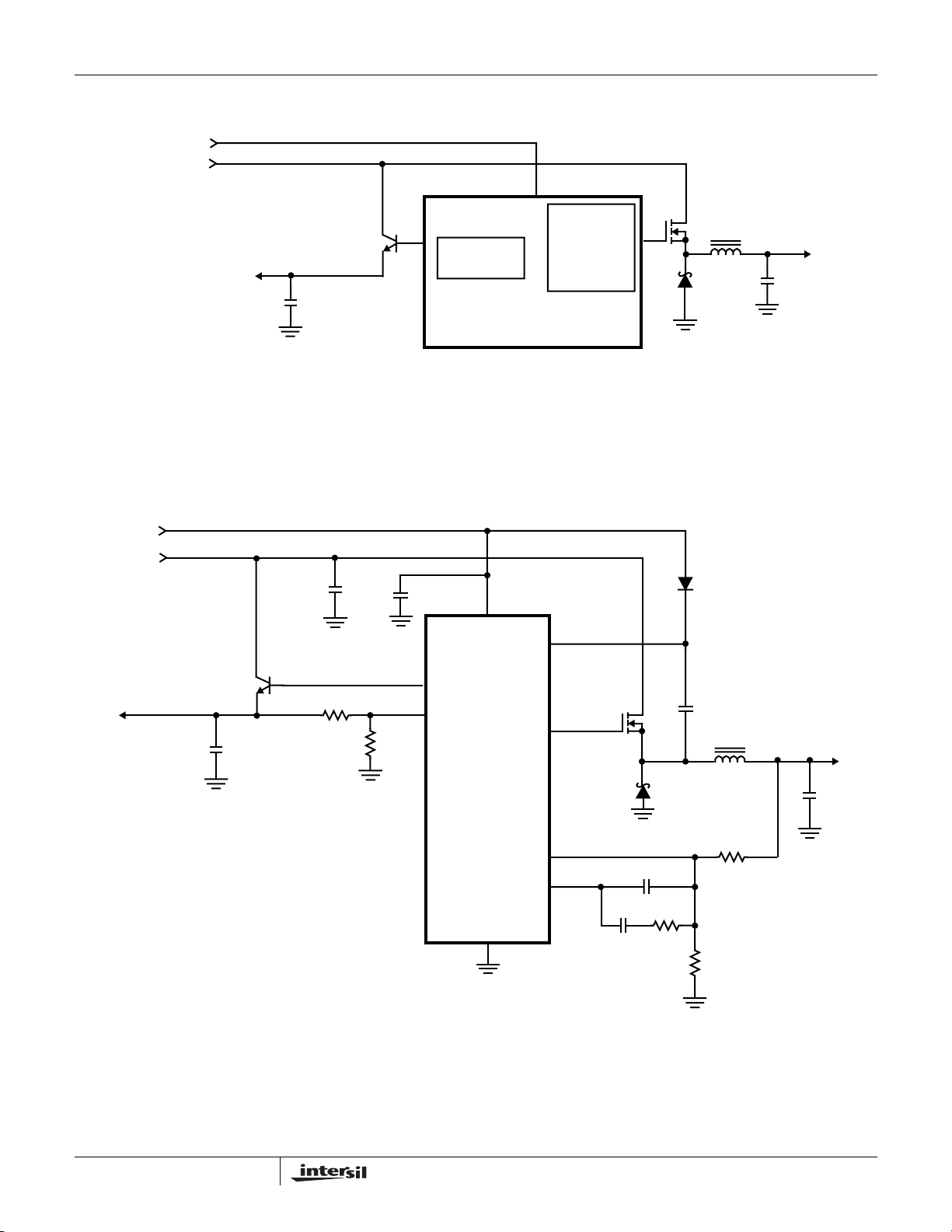
Simplified Power System Diagram
+5V
+3.3V
ISL6528
Typical Application
+5V
+3.3V
V
OUT2
2.5V
+
C
Q2
OUT2
V
OUT2
Q2
+
LINEAR
CONTROLLER
PWM
CONTROLLER
Q1
D1
V
OUT1
+
ISL6528
+
C
IN
DRIVE2
FB2
C
BP
VCC
BOOT
UGATE
Q1
PHASE
D2
C
BOOT
L
OUT
V
OUT1
1.5V
ISL6528
GND
D1
FB
COMP
+
C
OUT1
3
Page 4
∆
Ω
Ω
ISL6528
Absolute Maximum Ratings Thermal Information
UGATE, BOOT. . . . . . . . . . . . . . . . . . . . . . . . . . GND -0.3V to +10V
VCC . . . . . . . . . . . . . . . . . . . . . . . . . . . . . . . . . . . GND -0.3V to +7V
FB, DRIVE2, FB2, COMP, . . . . . . . . . . . GND -0.3V to VCC +0.3V
ESD Classification . . . . . . . . . . . . . . . . . . . . . . . . . . . . . . . . Class 2
Thermal Resistance (Typical, Note 1)
SOIC Package . . . . . . . . . . . . . . . . . . . . . . . . . . . . 110
Maximum Junction Temperature (Plastic Package) . . . . . . . 150
Maximum Storage Temperature Range. . . . . . . . . . -65
Maximum Lead Temperature (Soldering 10s) . . . . . . . . . . . . 300
Operating Conditions
(SOIC - Lead Tips Only)
Supply Voltage on VCC . . . . . . . . . . . . . . . . . . . . . . . . . . +5V ±10%
Supply Voltage to drain of upper MOSFET . . . . . . . . . +3.3V ±10%
Ambient Temperature Range. . . . . . . . . . . . . . . . . . . . 0
Junction Temperature Range. . . . . . . . . . . . . . . . . . . 0
CAUTION: Stresses above those listed in “Absolute Maximum Ratings” may cause permanent damage to the device. This is a stress only rating and operation of the
device at these or any other conditions above those indicated in the operational sections of this specification is not implied.
o
C to 70
o
C to 125
o
C
o
C
NOTE:
1.
is measured with the component mounted on a high effective thermal conductivity test board in free air. See Tech Brief TB379 for details.
θ
JA
θ
(
JA
o
C to 150
o
C/W)
o
o
o
C
C
C
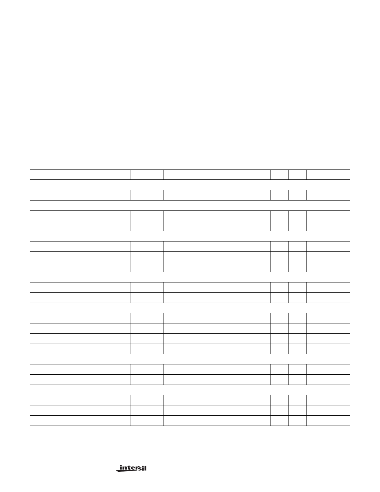
Electrical Specifications Recommended Operating Conditions, Unless Otherwise Noted. Refer to Block and Simplified Power System
Diagrams, and Typical Application Schematic
PARAMETER SYMBOL TEST CONDITIONS MIN TYP MAX UNITS
VCC SUPPLY CURRENT
Nominal Supply Current I
CC
UGATE and DRIVE2 Open 2 3.7 6.5 mA
POWER-ON RESET
Rising VCC Threshold 4.25 4.4 4.50 V
Falling VCC Threshold 3.75 3.8 4.00 V
OSCILLATOR AND SOFT-START
Free Running Frequency F
Ramp Amplitude
Soft-Start Interval T
OSC
V
OSC
SS
550 600 650 kHz
- 1.5 - V
P-P
3.10 3.42 3.75 ms
REFERENCE VOLTAGE
Reference Voltage V
REF
.784 0.800 .816 V
System Accuracy -2.00 - +2.00 %
PWM CONTROLLER ERROR AMPLIFIER
DC Gain -80- dB
Gain-Bandwidth Product GBWP 15 - - MHz
Slew Rate SR - 6 - V/ µ s
Undervoltage Level (V
FB
/V
)V
REF
UV
48.13 52.5 56.88 %
PWM CONTROLLER GATE DRIVER
UGATE Source Impedance R
UGATE Sink Impedance R
UGATE
UGATE
VCC = 5V, V
V
UGATE-PHASE
= 2.5V - 2.75 5.0
UGATE
= 2.5V - 3.0 5.0
LINEAR REGULATOR ERROR AMPLIFIER
Output Drive Current VCC > 4.5V 100 120 - mA
Overvoltage Level (V
Undervoltage Level (V
FB2
FB2
/V
)V
REF
/V
)V
REF
OV
UV
150.0 160.0 175.0 %
48.13 52.5 56.88 %
4
Page 5

ISL6528
Functional Pin Descriptions
8
7
6
5
UGATE
BOOT
COMP
FB
GND
1
2
VCC
FB2
3
4
DRIVE2
GND (Pin 1)
Signal ground for the IC. All voltage levels are measured
with respect to this pin. Place via close to pin to minimize
impedance path to ground plane.
VCC (Pin 2)
Provide a well decoupled 5V bias supply for the IC to this
pin. The voltage at this pin is monitored for Power-On Reset
(POR) purposes.
DRIVE2 (Pin 3)
Connect this pin to the base terminal of an external bipolar
NPN transistor. This pin provides the base current drive for
the linear regulator pass transistor.
FB2 (Pin 4)
Connect the output of the linear regulator to this pin through
a properly sized resistor divider. The voltage at this pin is
regulated to 0.8V. This pin is also monitored for undervoltage
events.
Pulling and holding FB2 above 1.25V shuts down both
regulators. Releasing FB2 initiates soft-start on both
regulators.
FB (Pin 5) and COMP (Pin 6)
FB and COMP are the available external pins of the error
amplifier. The FB pin is the inverting input of the error amplifier
and the COMP pin is the error amplifier output. These pins are
used to compensate the voltage-mode control feedback loop of
the standard buck converter.
BOOT (Pin 7)
Connect a suitable capacitor (0.47 µ F recommended) from
this pin to the source terminal of the upper MOSFET
(PHASE node). This bootstrap capacitor supplies the
UGATE driver the energy necessary to turn and hold the
upper MOSFET on.
BOOT must be kept below 10V
VCC and 3.3V drain supply to the upper MOSFET.
The absolute maximum voltage on
. This can be met with a 5V
UGATE (Pin 8)
Connect UGATE to the upper MOSFET gate. This pin
provides the gate drive for the MOSFET.
Description
Operation Overview
The ISL6528 monitors and precisely controls two output
voltage levels. Refer to the
Power System Diagram
on pp. 2–3. The controller is intended for use in graphics
card or embedded processor applications with 3.3V and 5V
bias input available. The IC integrates both a standard buck
PWM controller and a linear controller. The PWM controller
is designed to regulate the high current GPU voltage
(V
MOSFET (Q1) in a standard buck converter configuration
and regulates the output voltage to a level programmed by
a resistor divider. The linear controller is designed to
regulate the lower current local memory voltage (V
through an external NPN pass transistor.
). The PWM controller drives a single N-Channel
OUT1
Initialization
The ISL6528 automatically initializes upon application of
input power. Special sequencing of the input supplies is not
necessary. The POR function continually monitors the input
bias supply voltage at the VCC pin. The POR function
initiates soft-start operation after the 5V bias supply voltage
exceeds its POR threshold.
Soft-Start
The POR function initiates the digital soft-start sequence.
Both the linear regulator error amplifier and PWM error
amplifier reference inputs are forced to track a voltage level
proportional to the soft-start voltage. As the soft-start voltage
slews up, the PWM comparator regulates the output relative
to the tracked soft-start voltage slowly charging the output
capacitor(s). Simultaneously, the linear output follows the
smooth ramp of the soft-start function into normal regulation.
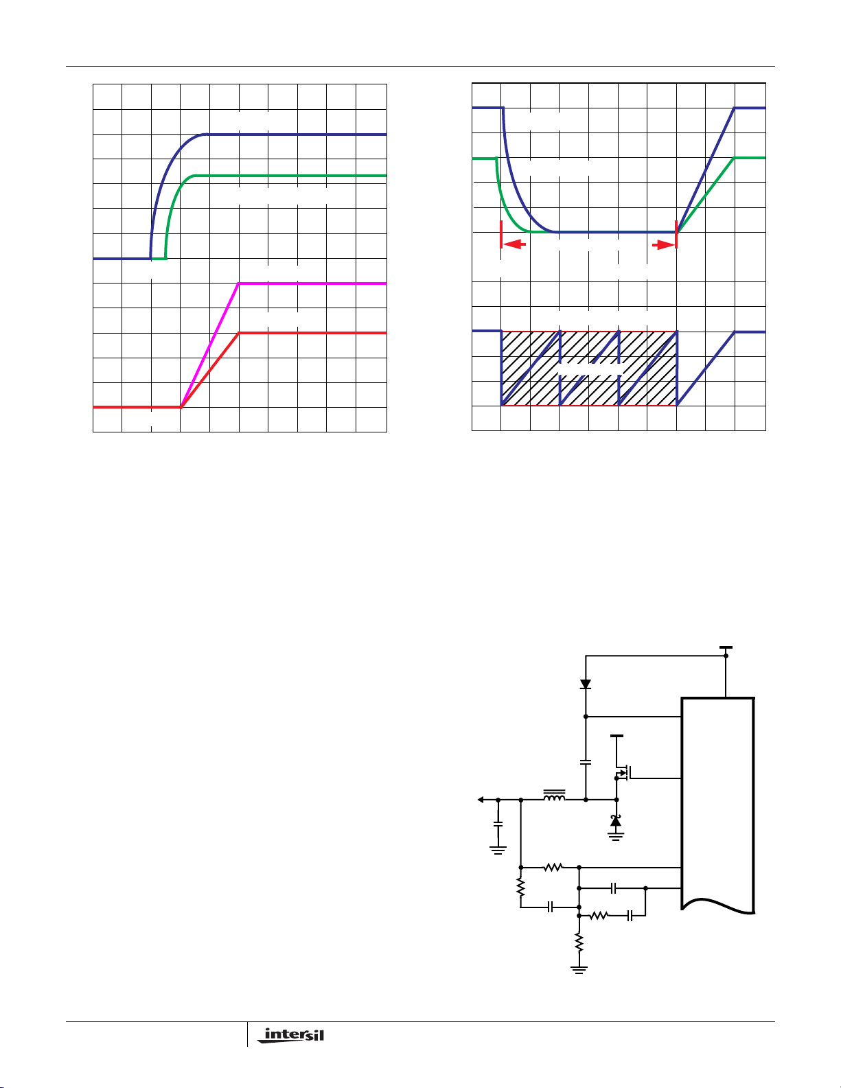
Figure 1 shows the soft-start sequence for a typical application.
At T0, the +5V VCC bias voltage starts to ramp followed by the
3.3V input supply. Once the voltage on VCC crosses the 4.4V
POR threshold at time T1, both outputs begin their soft-start
sequence. The triangle waveform from the PWM oscillator is
compared to the rising error amplifier output voltage. As the
error amplifier voltage increases, the pulse-width on the
UGATE pin increases to reach its steady-state duty cycle at
time T2. The error amplifier reference of the linear controller
also rises relative to the soft-start reference. The resulting soft
ramp on DRIVE2 brings V
T2.
Undervoltage Protection
The FB and FB2 pins are monitored during converter
operation by two separate undervoltage (UV) comparators. If
the FB voltage drops below 52.5% of the reference voltage
(0.42V), a fault signal is generated. The internal fault logic
Block Diagram, Simplified
, and Typical Application Schematic
)
OUT2
within regulation limits by time
OUT2
5
Page 6
µ
Ω
+5V (VCC)
R4
R1 0.8V×
V
OUT1
0.8V–
--------------------------------------=
(EQ. 1)
FIGURE 2. UNDERVOLTAGE PROTECTION RESPONSE
0V
0V
TIME
V
OUT2
(2.5V)
T1 T2
T3
T0 T4
(0.5V/DIV)
V
OUT1
(1.5V)
Internal Soft-Start Function
V
OUT2
(2.5V)
Delay Interval
Delay Interval
FIGURE 3. OUTPUT VOLTAGE SELECTION OF THE PWM
+
R1
C
OUT1
+5V
+3.3V
V
OUT1
R4
L
OUT
ISL6528
C4
Q1
FB
UGATE
VCC
BOOT
COMP
D1
D2
R2
C1
C2
R3
C3
+3.3V (UPPER FET DRAIN)
ISL6528
0V
0V
(1V/DIV)
(0.5V/DIV)
T0
T1
T2
TIME
V
V
OUT2
OUT1
(2.5V)
(1.5V)
FIGURE 1. SOFT-START INTERVAL
shuts down both regulators simultaneously when the fault
signal triggers a restart.
Figure 2 illustrates the protection feature responding to an
UV event on V
. At time T0, VOUT1 has dropped below
OUT1
52.5% of the nominal output voltage. Both outputs are
quickly shut down and the internal soft-start function begins
producing soft-start ramps. The delay interval, T0 to T3,
seen by the output is equivalent to three soft-start cycles.
After a short delay interval of 10.5ms, the fourth internal softstart cycle initiates a normal soft-start ramp of the output, at
time T3. Both outputs are brought back into regulation by
time T4, as long as the UV event has cleared.
value chosen for R1, R4 can be calculated based on the
following equation:
If the output voltage desired is 0.8V, simply route VOUT1
back to the FB pin through R1, but do not populate R4.
Had the cause of the UV still been present after the delay
interval, the UV protection circuitry becomes active
approximately 875
could then be generated and the outputs once again
shutdown. The resulting hiccup mode style of protection
would continue to repeat indefinitely.
Output Voltage Selection
The output voltage of the PWM converter can be
programmed to any level between V
internal reference, 0.8V. An external resistor divider is used
to scale the output voltage relative to the reference voltage
and feed it back to the inverting input of the error amplifier,
see Figure 3. However, since the value of R1 affects the
values of the rest of the compensation components, it is
advisable to keep its value less than 5k
s into the soft-start interval. A fault signal
6
(i.e. +3.3V) and the
IN
. Depending on the
Page 7
Ω
Ω
F
LC
1
2π L
OCO
××
----------------------------------------=
F
ESR
1
2π ESR CO××
-----------------------------------------=
(EQ. 5)
(EQ. 6)
FIGURE 5. VOLTAGE-MODE BUCK CONVERTER
COMPENSATION DESIGN
V
OUT
V
REF
L
OUT
C
O
ESR
V
IN
∆V
OSC
ERROR
AMP
PWM
DRIVER
(PARASITIC)
+
-
0.8V
R1
R3
R2
C3
C2
C1
COMP
V
OUT
FB
Z
FB
ISL6528
Z
IN
COMP
DETAILED COMPENSATION COMPONENTS
PHASE
V
E/A
+
-
+
+
Z
FB
Z
IN
OSC
ISL6528
+3.3V
IN
Q2
V
OUT2
R5
--------+
R6
R5
+
C
OUT2
V
OUT2
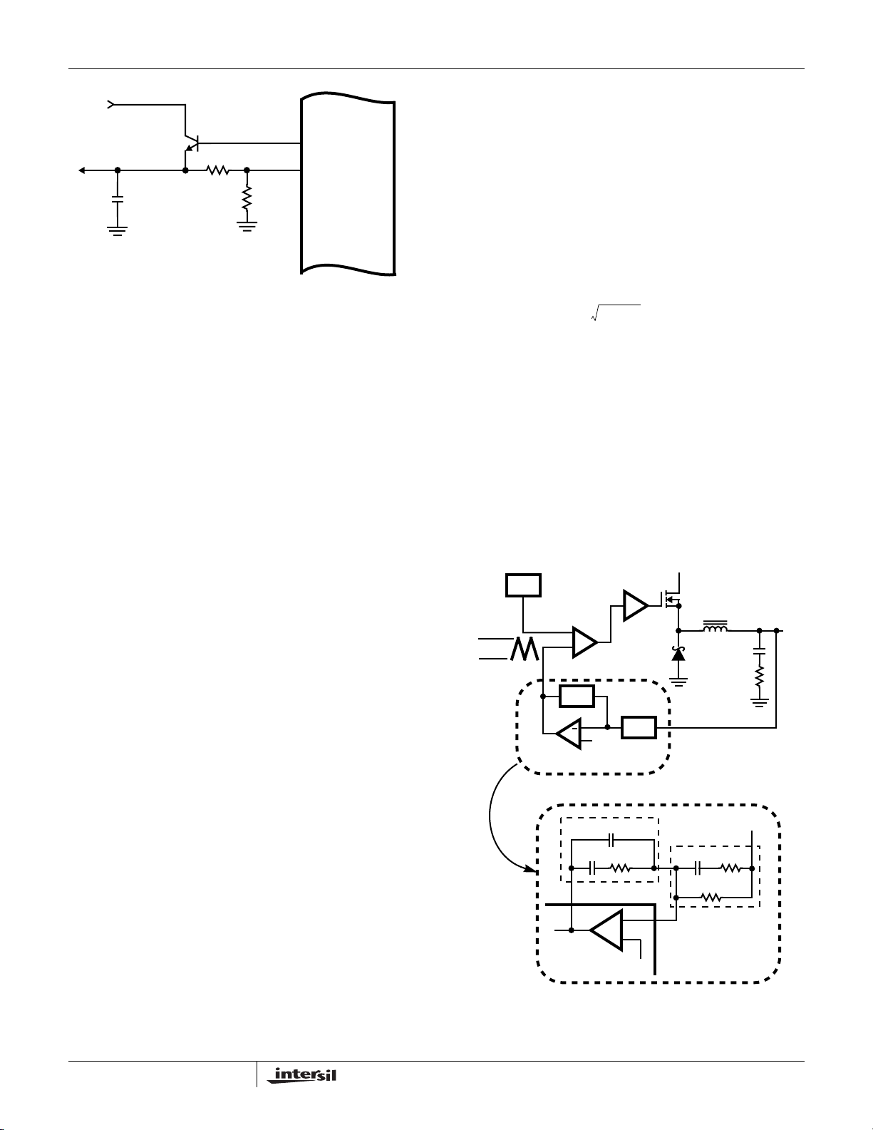
FIGURE 4. OUTPUT VOLTAGE SELECTION OF THE LINEAR
0.8 1
×=
DRIVE2
R6
The linear regulator output voltage is also set by means of
an external resistor divider as shown in Figure 4. The two
resistors used to set the output voltage should not exceed a
parallel equivalent value, referred to as R
restriction is due to the manner of implementation of the softstart function. The following relationship must be met:
R5 R6×
R
FB
----------------------
R5 R6+
5kΩ<=
To ensure the parallel combination of the feedback resistors
meets this criteria, choose a target value for R
5k
and then apply the following equations:
V
OUT2
R
×=
REF
R5 V
OUT2VREF
FB
×
REF
–
R5
-------------------
V
R6
-----------------------------------------=
V
where V
and V
REF
output voltage of 0.8V, simply populate R5 with a value less
than 5k
Converter Shutdown
is the desired linear regulator output voltage
OUT2
is the internal reference voltage, 0.8V. For an
and do not populate R6.
Pulling and holding the FB2 pin above a typical threshold of
1.28V will shutdown both regulators. Upon release of the
FB2 pin, the regulators enter into a soft-start cycle which
brings both outputs back into regulation.
PWM Controller Feedback Compensation
A simplified representation of the voltage-mode control loop
used for output regulation by the standard buck converter is
shown in Figure 5. The output voltage, V
, to provide a pulse-width modulated (PWM)
OSC
IN
the negative input of the error amplifier which is regulated to
the reference voltage level, V
V
, is compared with the triangle wave produced by the
E/A
oscillator, V
signal from the PWM comparator. This signal is then used to
switch the MOSFET and produce a PWM waveform with an
amplitude of V
. The error amplifier output,
REF
at the PHASE node. The square-wave
7
FB2
FB
(EQ. 2)
OUT
ISL6528
, of 5k Ω . This
(EQ. 3)
(EQ. 4)
of less than
FB
, is fed back to
PHASE voltage is then smoothed by the output filter, L
and C
The modulator transfer function is defined as V
, to produce a DC voltage level.
OUT
OUT
/V
E/A
OUT
.
The internal PWM comparator and driver circuits equate to a
DC gain block dominated by the supply voltage, V
by the peak-to-peak magnitude of the triangle wave,
The output filter components, L
OUT
and C
OUT
, divided
IN
∆
V
OSC
, shape the
overall modulator small-signal transfer function by
contributing a double pole break frequency at F
zero at F
ESR
.
LC
and a
Modulator Break Frequency Equations
The compensation network consists of the error amplifier
and the impedance networks Z
link between the modulator transfer function and a
controllable closed loop transfer function of V
goal of component selection for the compensation network is
to provide a loop gain with high 0dB crossing frequency
(f
) and adequate phase margin. Phase margin is the
0dB
difference between the closed loop phase at f
degrees.
and Z
IN
. They provide the
FB
/V
OUT
REF
and 180
0dB
. The
.
Page 8
ISL6528
Compensation Break Frequency Equations
Poles:
F
-------------------------------------------------------=
P1
2π R
F
-----------------------------------=
2π R× 3C3×
P2
Zeros:
F
-----------------------------------=
2π R× 2C1×
Z1
-------------------------------------------------------=
F
2π R1 R3+()C3××
Z2
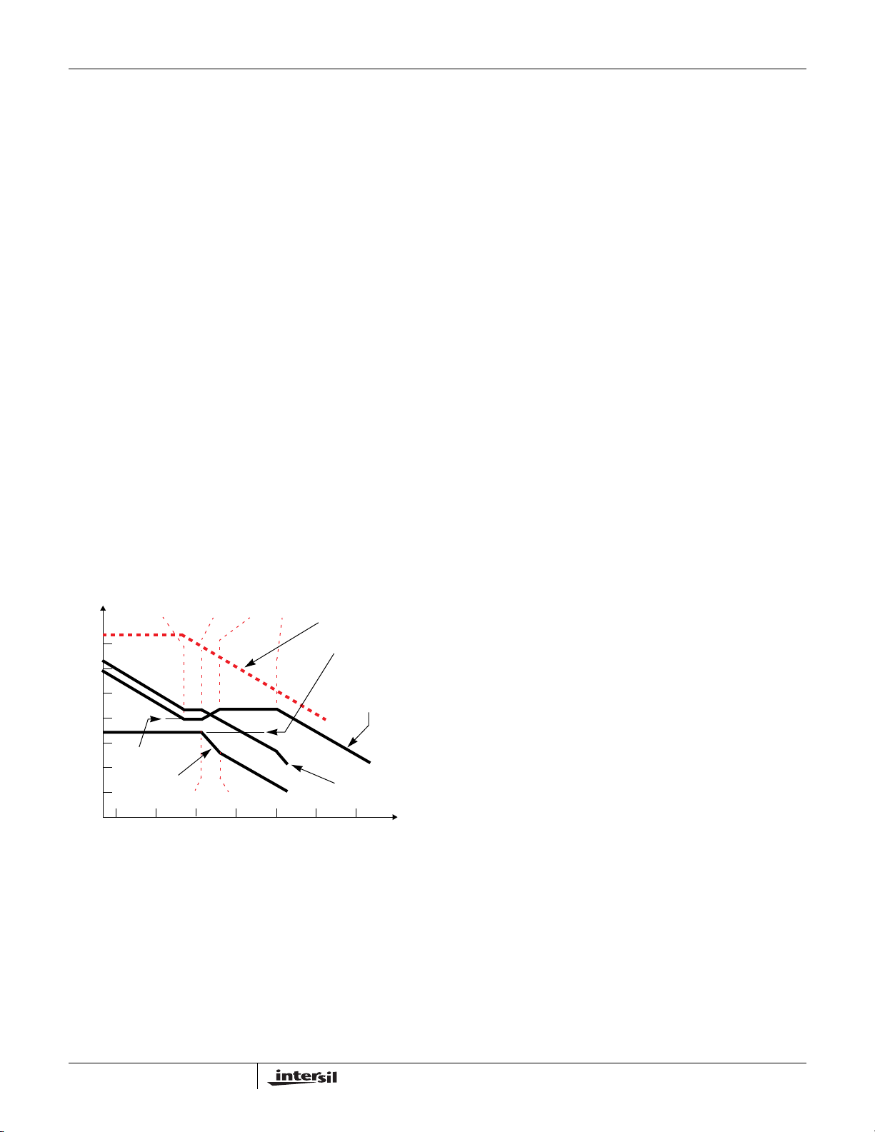
Follow this procedure for selecting compensation
components by locating the poles and zeros of the
compensation network:
1. Set the loop gain (R2/R1) to provide a converter
bandwidth of one quarter of the switching frequency.
2. Place the first
compensation zero, FZ1, below the output
filter double pole (~75% F
3. Position the second compensation zero, F
output filter double pole, F
4. Locate the first compensation pole, F
ESR zero, F
ESR
.
5. Position the second compensation pole at half the
converter switching frequency, F
6. Check gain against error amplifier’s open-loop gain.
7. Estimate phase margin; repeat if necessary.
8.
F
log
GAIN
Z1
R2
---------
R1
100
80
60
40
20
GAIN (dB)
0
20
-20
MODULATOR
-40
-60
FIGURE 6. ASYMPTOTIC BODE PLOT OF CONVERTER GAIN
Figure 6 shows an asymptotic plot of the DC-DC converter’s
gain vs. frequency. The actual modulator gain has a high
gain peak dependent on the quality factor (Q) of the output
filter, which is not shown in Figure 6. Using the above
procedure should yield a compensation gain similar to the
curve plotted. The open loop error amplifier gain bounds the
compensation gain. Check the compensation gain at F
with the capabilities of the error amplifier.
1
C1 C2×
××
2
----------------------
C1 C2+
1
1
1
LC
F
Z2
F
F
LC
ESR
FREQUENCY (Hz)
LC
F
(EQ. 8)
(EQ. 9)
(EQ. 10)
(EQ. 11)
).
, at the
Z2
.
, at the output filter
P1
.
SW
F
P1
P2
OPEN LOOP
ERROR AMP GAIN
V
20
COMPENSATION
IN
log
------------------
V
OSC
GAIN
LOOP GAIN
10M1M100K10K1K10010
P2
The compensation gain uses external impedance networks
Z
and ZIN to provide a stable, high bandwidth (BW)
FB
overall loop. A stable control loop has a gain crossing with
-20dB/decade slope and a phase margin greater than 45˚.
Include worst case component variations when determining
phase margin.
Application Guidelines
Layout Considerations
Layout is very important in high frequency switching
converter design. With power devices switching efficiently at
600kHz, the resulting current transitions from one device to
another cause voltage spikes across the interconnecting
impedances and parasitic circuit elements. These voltage
spikes can degrade efficiency, radiate noise into the circuit,
and lead to device overvoltage stress. Careful component
layout and printed circuit board design minimizes the voltage
spikes in the converters.
As an example, consider the turn-off transition of the PWM
MOSFET. Prior to turn-off, the MOSFET is carrying the full
load current. During turn-off, current stops flowing in the
MOSFET and is picked up by the lower Schottky diode. Any
parasitic inductance in the switched current path generates
a large voltage spike during the switching interval. Careful
component selection, tight layout of the critical components,
and short, wide traces minimizes the magnitude of voltage
spikes.
There are two sets of critical components in a DC-DC
converter using the ISL6528. The switching components are
the most critical because they switch large amounts of
energy, and therefore tend to generate large amounts of
noise. Next are the small signal components which connect
to sensitive nodes or supply critical bypass current and
signal coupling.
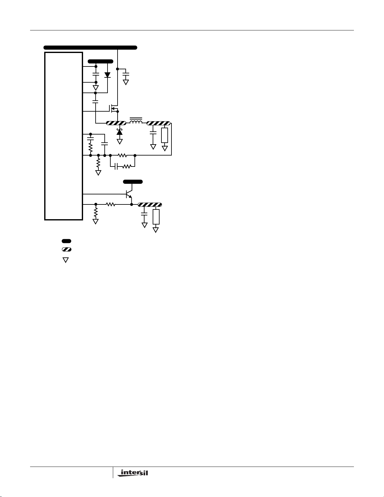
A multi-layer printed circuit board is recommended. Figure 7
shows the connections of the critical components in the
converter. Note that capacitors C
represent numerous physical capacitors. Dedicate one solid
layer, usually a middle layer of the PC board, for a ground
plane and make all critical component ground connections
through vias to this layer. Dedicate another solid layer as a
power plane and break this plane into smaller islands of
common voltage levels. Keep the metal runs from the
PHASE terminal to the output inductor short. The power
plane should support the input and output power nodes. Use
copper filled polygons on the top and bottom circuit layers
for the phase node. Use the remaining printed circuit layers
for small signal wiring. The wiring traces from the UGATE pin
to the MOSFET gate should be kept short and wide enough
to easily handle the 1A of drive current.
The switching components should be placed close to the
ISL6528 first. Minimize the length of the connections
between the input capacitors, C
and C
IN
, and the power switches
IN
could each
OUT
8
Page 9
∆I
V
INVOUT
–
F
S
L×
--------------------------------
V
OUT
V
IN
----------------
×=
V
OUT
∆ I∆ ESR×=
(EQ. 11)
(EQ. 12)
ISL6528
+3.3 V
IN
+5 VCC
VCC
C
Q1
L
IN
OUT
V
OUT1
GND
BOOT
UGATE
C
BP
C
BOOT
PHASE
D2
ISL6528
C
R5
D1
C
OUT1
1
R1
C
R
3
3
+3.3 V
IN
Q2
V
OUT2
C
OUT2
BP
LOAD
LOAD
, close to
COMP
FB
DRIVE2
FB2
KEY
ISLAND ON POWER PLANE LAYER
ISLAND ON CIRCUIT PLANE LAYER
VIA CONNECTION TO GROUND PLANE
FIGURE 7. PRINTED CIRCUIT BOARD POWER PLANES AND
C
2
R
2
R4
R6
ISLANDS
by placing them nearby. Position both the ceramic and bulk
input capacitors as close to the upper MOSFET drain as
possible. Position the output inductor and output capacitors
between the upper MOSFET and lower diode and the load.
The critical small signal components include any bypass
capacitors, feedback components, and compensation
components. Position the bypass capacitor, C
the VCC pin with a via directly to the ground plane. Place the
PWM converter compensation components close to the FB
and COMP pins. The feedback resistors for both regulators
should also be located as close as possible to the relevant
FB pin with vias tied straight to the ground plane as required.
Component Selection Guidelines
PWM REGULATOR OUTPUT CAPACITORS
Modern digital ICs can produce high transient load slew
rates. High frequency capacitors initially supply the transient
current and slow the load rate-of-change seen by the bulk
capacitors. The bulk filter capacitor selection is generally
determined by the effective series resistance (ESR) and
voltage rating requirements rather than actual capacitance
requirements.
High frequency decoupling capacitors should be placed as
close to the power pins of the load as physically possible. Be
careful not to add inductance in the circuit board wiring that
could cancel the usefulness of these low inductance
components. Consult with the manufacturer of the load on
specific decoupling requirements.
Specialized low-ESR capacitors intended for switchingregulator applications are recommended for the bulk
capacitors. The bulk capacitor’s ESR determines the output
ripple voltage and the initial voltage drop following a high
slew-rate transient edge. Aluminum electrolytic, tantalum,
and special polymer capacitor ESR values are related to the
case size with lower ESR available in larger case sizes.
However, the equivalent series inductance (ESL) of these
capacitors increases with case size and can reduce the
usefulness of the capacitor to high slew-rate transient
loading. Unfortunately, ESL is not a specified parameter.
Work with your capacitor supplier and measure the
capacitor’s impedance with frequency to select a suitable
component. In most cases, multiple electrolytic capacitors of
small case size perform better than a single large case
capacitor.
LINEAR REGULATOR OUTPUT CAPACITORS
The output capacitors for the linear regulator provide
dynamic load current. The linear controller uses dominant
pole compensation integrated into the error amplifier and is
relatively insensitive to output capacitor selection. Output
capacitors should be selected for transient load regulation.
PWM Output Inductor Selection
The PWM converter requires an output inductor. The output
inductor is selected to meet the output voltage ripple
requirements and sets the converter response time to a load
transient. The inductor value determines the converter’s
ripple current and the ripple voltage is also a function of the
ripple current. The ripple voltage and current are
approximated by the following equations:
Output Capacitor Selection
Output capacitors are required to filter the output and supply
the load transient current. The filtering requirements are a
function of switching frequency and output current ripple.
The load transient requirements are a function of the
transient load current slew rate (di/dt) and magnitude. These
requirements are generally met with a mix of capacitors and
careful layout.
9
Increasing the value of inductance reduces the output ripple
current and voltage ripple. However, increasing the
Page 10

P
ConductionIo
2
r
DS on()
× D×≅
P
Switching
1
2
---IoVIN× tSW× FSW×≅
(EQ. 15)
(EQ. 16)
ISL6528
inductance value will slow the converter response time to a
load transient.
One of the parameters limiting the converter’s response to a
load transient is the time required to slew the inductor
current. Given a sufficiently fast control loop design, the
ISL6528 will provide either 0% or 100% duty cycle in
response to a load transient. The response time is the time
interval required to slew the inductor current from an initial
current value to the final current level. During this interval the
difference between the inductor current and the load current
must be supplied by the output capacitor(s). Minimizing the
response time can minimize the output capacitance
required.
The response time to a transient is different for the
application of load and the removal of load. The following
equations give the approximate response time interval for
application and removal of a transient load:
LOI
×
t
RISE
t
FALL
TRAN
--------------------------------=
V
–
INVOUT
LOI
×
-------------------------------=
V
OUT
TRAN
(EQ. 13)
(EQ. 14)
For a through-hole design, several aluminum electrolytic
capacitors may be needed. For surface mount designs,
tantalum or special polymer capacitors can be used, but
caution must be exercised with regard to the capacitor surge
current rating. These capacitors must be capable of handling
the surge-current at power-up.
Transistor Selection/Considerations
The ISL6528 requires two external transistors. One Nchannel MOSFET is used as the upper switch in a standard
buck topology PWM converter. The linear controller drives
an NPN bipolar transistor as a pass element. The transistors
should be selected based upon r
DS(ON)
saturation voltages, gate/base supply requirements, and
thermal management considerations.
UPPER MOSFET SWITCH SELECTION
In high-current applications, the MOSFET power dissipation,
package selection and heatsink are the dominant design
factors. The power dissipation includes two loss
components; conduction loss and switching loss. The
conduction losses account for a large portion of the power
dissipation of the MOSFET. Switching losses also contribute
to the overall MOSFET power loss.
, current gain,
where I
response time to the application of load, and t
is the transient load current step, t
TRAN
RISE
FALL
is the
is the
response time to the removal of load.
With a +3.3V input source, the worst case response time can
be either at the application or removal of load and
dependent upon the output voltage setting. Be sure to check
both of these equations at the minimum and maximum
output levels for the worst case response time.
Input Capacitor Selection
The important parameters for the bulk input capacitors are
the voltage rating and the RMS current rating. For reliable
operation, select bulk input capacitors with voltage and
current ratings above the maximum input voltage and largest
RMS current required by the circuit. The capacitor voltage
rating should be at least 1.25 times greater than the
maximum input voltage and a voltage rating of 1.5 times is a
conservative guideline. The RMS current rating requirement
for the input capacitor of a buck regulator is approximately
1/2 of the summation of the DC load current.
Use a mix of input bypass capacitors to control the voltage
overshoot across the MOSFETs. Use ceramic capacitance
for the high frequency decoupling and bulk capacitors to
supply the RMS current. Small ceramic capacitors can be
placed very close to the upper MOSFET to suppress the
voltage induced in the parasitic circuit impedances. Connect
them directly to ground with a via placed very close to the
ceramic capacitor footprint.
where I
the converter (defined as V
interval, and F
is the maximum load current, D is the duty cycle of
o
is the PWM switching frequency.
SW
), tSW is the switching
O/VIN
These equations assume linear voltage-current transitions
and are approximations. The gate-charge losses are
dissipated by the ISL6528 and do not heat the MOSFET.
However, large gate-charge increases the switching interval,
t
, which increases the upper MOSFET switching losses.
SW
Ensure that the MOSFET is within its maximum junction
temperature at high ambient temperature by calculating the
temperature rise according to package thermal-resistance
specifications. A separate heatsink may be necessary
depending upon MOSFET power, package type, ambient
temperature, air flow, and load current requirements.
Given the reduced available gate bias voltage (5V) a logiclevel transistor is recommended for the upper switch. Close
attention to layout guidelines should be exercised with
devices exhibiting very low V
characteristics, as the
GS(on)
low gate threshold could lead to some shoot-through despite
counteracting circuitry present aboard the ISL6528.
NPN PASS TRANSISTOR SELECTION
A bipolar NPN transistor must be used with the linear
controller. Insure the current gain at the given operating V
CE
is sufficiently large to provide the desired maximum output
10
Page 11
load current when the base is fed with the minimum driver
Q1
D1
C
BOOT
BOOT
UGATE
PHASE
VCC
+3.3V
+5V
D2
ISL6528
FIGURE 8. UPPER GATE DRIVE
C
BOOT
Q
GATE
V
BOOT1
V–
BOOT2
-----------------------------------------------------
≥
(EQ. 20)
output current.
The main criteria for selection of the linear regulator pass
transistor is package selection for efficient removal of heat.
Select a package and heatsink that maintains the junction
temperature below the rating with a maximum expected
ambient temperature.
The power dissipated in a linear regulator is:
ISL6528
where I
P
LINEARIOVINVOUT
is the maximum output current and V
O
–()×≅
(EQ. 17)
OUT
is the
nominal output voltage of the linear regulator.
Diode Selection (D1)
Rectifier D1 conducts when MOSFET Q1 is off. The diode
should be a Schottky type for low power losses. The power
dissipation in the Schottky rectifier is approximated by:
P
CONDUCTIONIOVf
where I
converter, V
is the maximum output current of the PWM
O
is the Schottky forward voltage drop, and D is
f
the duty cycle of the converter (defined as V
× 1D–()×≅
(EQ. 18)
).
O/VIN
In addition to power dissipation, package selection and
heatsink requirements are the main design trade-offs in
choosing a Schottky rectifier. Since the three factors are
interrelated, the selection process is an iterative procedure.
The maximum junction temperature of the rectifier must
remain below the manufacturer’s specified value, typically
125˚C. By using the package thermal resistance
specification and the Schottky power dissipation equation,
the junction temperature of the rectifier can be estimated. Be
sure to use the available airflow and ambient temperature to
determine the junction temperature rise.
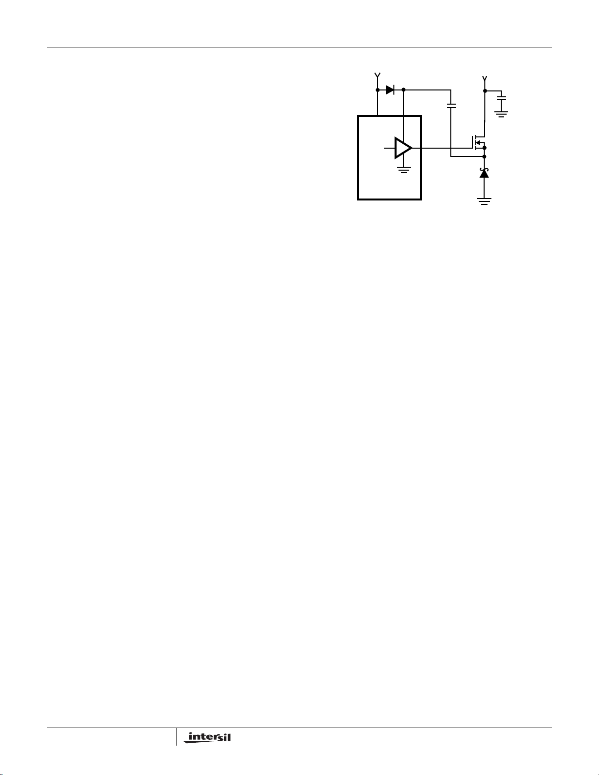
Bootstrap Component Selection
External bootstrap components, a diode and capacitor, are
required to provide sufficient gate enhancement to the
MOSFET. The internal MOSFET gate driver is supplied by
the external bootstrap circuitry as shown in Figure 8. The
boot capacitor, C
referenced to the PHASE pin. This supply is refreshed each
cycle, when D1 conducts, to a voltage of VCC less the boot
diode drop, V
Just after the PWM switching cycle begins and the charge
transfer from the bootstrap capacitor to the gate capacitance
is complete, the voltage on the bootstrap capacitor is at its
D2
lowest point during the switching cycle. The charge lost on
the bootstrap capacitor will be equal to the charge
transferred to the equivalent gate-source capacitance of the
MOSFET as shown in Equation 19.
Q
GATECBOOTVBOOT1VBOOT2
, develops a floating supply voltage
BOOT
, plus the voltage rise across D1.
–()×=
11
(EQ. 19)
where Q
MOSFET, C
is the maximum total gate charge of the
GATE
is the bootstrap capacitance, V
BOOT
BOOT1
is
the bootstrap voltage immediately before turn-on, and
V
is the bootstrap voltage immediately after turn-on.
BOOT2
The bootstrap capacitor begins its refresh cycle when the
gate drive begins to turn off the MOSFET. A refresh cycle
ends when the MOSFET is turned on again, which varies
depending on the switching frequency and duty cycle.
The minimum bootstrap capacitance can be calculated by
rearranging Equation 19 and solving for C
BOOT
.
Typical gate charge values for MOSFETs considered in
these types of applications range from 20–100nC. Since the
voltage drop across D2 is offset by the voltage drop across
D1, V
is simply VCC (+5V). A good rule is to keep the
BOOT1
voltage drop across the bootstrap capacitor no greater than
1V during the on-time of the MOSFET. Initial calculations
with V
no less than 4V will quickly help narrow the
BOOT2
bootstrap capacitor range.
For example, consider a MOSFET is chosen with a
maximum gate charge, Q
, of 100nC. Limiting the voltage
g
drop across the bootstrap capacitor to 1V results in a value
of no less than 0.1µF. The tolerance of the ceramic capacitor
should also be considered when selecting the final bootstrap
capacitance value.
A fast recovery diode is recommended when selecting a
bootstrap diode to reduce the impact of reverse recovery
charge loss. Otherwise, the recovery charge, Q
RR
, would
have to be added to the gate charge of the MOSFET and
taken into consideration when calculating the minimum
bootstrap capacitance. Employing a Schottky diode over a
standard diode will also increase the gate drive voltage
available to enhance the MOSFET.
Page 12
ISL6528
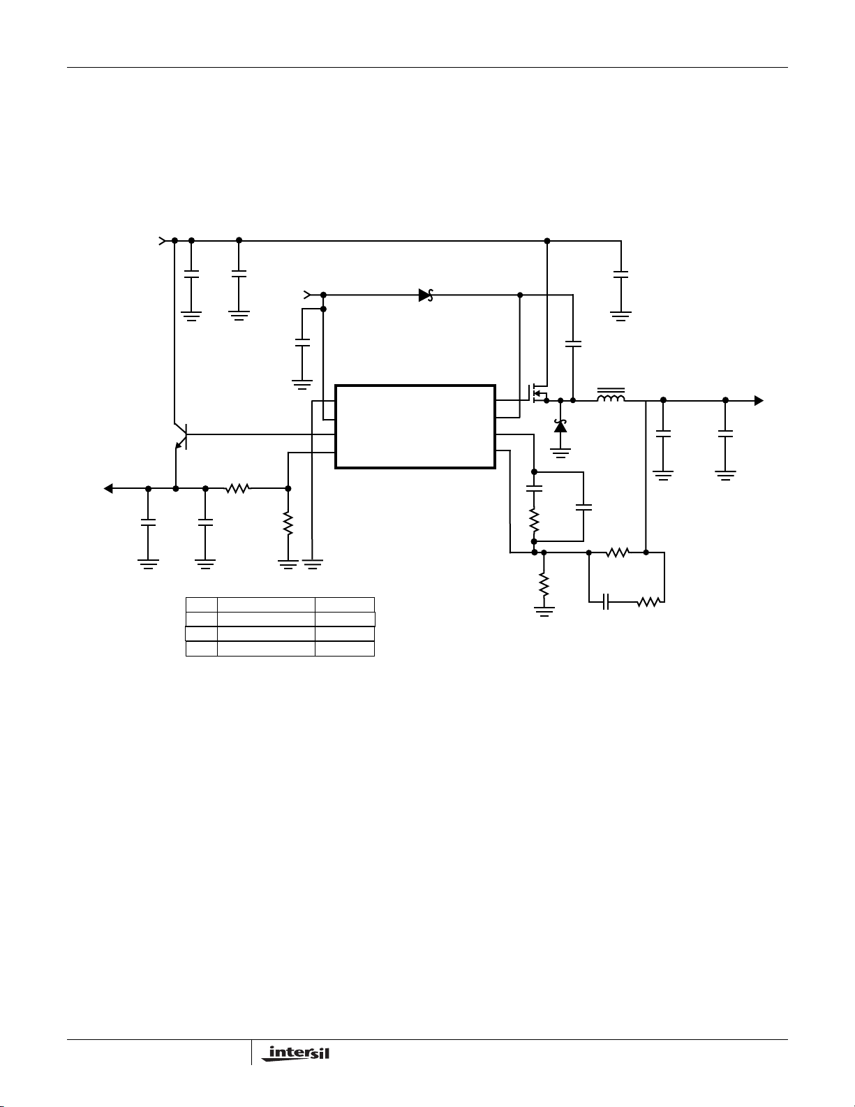
ISL6528 Converter Application Circuit
Figure 9 shows a typical DC-DC converter circuit for a graphics card application. Additional information on this circuit
can be obtained by referencing application note AN9982.
+3.3V
VOUT2
(1A)
Q2
C14
1µF
C6
330µF
R5
11.3kΩ
C12
470µF
Q1
FDS6690A
FZT649
Q2
L1
ETQ-P6F1R8BFA
B520C-13
D1
C7
330µF
R6
5.36kΩ
C5
1µF
+5V
GND
VCC
DRIVE2
FB2
Fairchild
Fairchild
Panasonic
Diode Inc.
D2
BAT54
ISL6528
UGATE
BOOT
COMP
FB
Q1
C1
150pF
R2
39.2kΩ
R4
2.67kΩ
D1
C4
0.1µF
1.71µH
C2
1500pF
C1
0.018µF
L1
R1
2.32kΩ
C8
1µF
R2
30.9Ω
C9,C10
2x470µF
VOUT1
(6A)
C11
1µF
FIGURE 9. POWER SUPPLY APPLICATION CIRCUIT FOR A GRAPHICS CONTROLLER
12
Page 13
Small Outline Plastic Packages (SOIC)
ISL6528
N
INDEX
AREA
123
SEATING PLANE
-AD
e
B
0.25(0.010) C AM BS
M
E
-B-
A
-C-
0.25(0.010) BM M
H
α
µ
A1
0.10(0.004)
L
h x 45
o
C
NOTES:
1. Symbols are defined in the “MO Series Symbol List” in Section 2.2 of
Publication Number 95.
2. Dimensioning and tolerancing per ANSI Y14.5M-1982.
3. Dimension “D” does not include mold flash, protrusions or gate burrs.
Mold flash, protrusion and gate burrs shall not exceed 0.15mm (0.006
inch) per side.
4. Dimension “E” does not include interlead flash or protrusions. Interlead flash and protrusions shall not exceed 0.25mm (0.010 inch) per
side.
5. The chamfer on the body is optional. If it is not present, a visual index
feature must be located within the crosshatched area.
6. “L” is the length of terminal for soldering to a substrate.
7. “N” is the number of terminal positions.
8. Terminal numbers are shown for reference only.
9. The lead width “B”, as measured 0.36mm (0.014 inch) or greater
above the seating plane, shall not exceed a maximum value of
0.61mm (0.024 inch).
10. Controlling dimension: MILLIMETER. Converted inch dimensions
are not necessarily exact.
M8.15 (JEDEC MS-012-AA ISSUE C)
8 LEAD NARROW BODY SMALL OUTLINE PLASTIC
PACKAGE
INCHES MILLIMETERS
SYMBOL
A 0.0532 0.0688 1.35 1.75 -
A1 0.0040 0.0098 0.10 0.25 -
B 0.013 0.020 0.33 0.51 9
C 0.0075 0.0098 0.19 0.25 -
D 0.1890 0.1968 4.80 5.00 3
E 0.1497 0.1574 3.80 4.00 4
e 0.050 BSC 1.27 BSC -
H 0.2284 0.2440 5.80 6.20 -
h 0.0099 0.0196 0.25 0.50 5
L 0.016 0.050 0.40 1.27 6
N8 87
o
α
0
o
8
o
0
o
8
Rev. 0 12/93
NOTESMIN MAX MIN MAX
-
All Intersil U.S. products are manufactured, assembled and tested utilizing ISO9000 quality systems.
Intersil Corporation’s quality certifications can be viewed at www.intersil.com/design/quality
Intersil products are sold by description only. Intersil Corporation reserves the right to make changes in circuit design, software and/or specifications at any time without
notice. Accordingly, the reader is cautioned to verify that data sheets are current before placing orders. Information furnished by Intersil is believed to be accurate and
reliable. However, no responsibility is assumed by Intersil or its subsidiaries for its use; nor for any infringements of patents or other rights of third parties which may result
from its use. No license is granted by implication or otherwise under any patent or patent rights of Intersil or its subsidiaries.
For information regarding Intersil Corporation and its products, see www.intersil.com
Sales Office Headquarters
NORTH AMERICA
Intersil Corporation
7585 Irvine Center Drive
Suite 100
Irvine, CA 92618
TEL: (949) 341-7000
FAX: (949) 341-7123
Intersil Corporation
2401 Palm Bay Rd.
Palm Bay, FL 32905
TEL: (321) 724-7000
FAX: (321) 724-7946
13
EUROPE
Intersil Europe Sarl
Ave. William Graisse, 3
1006 Lausanne
Switzerland
TEL: +41 21 6140560
FAX: +41 21 6140579
ASIA
Intersil Corporation
Unit 1804 18/F Guangdong Water Building
83 Austin Road
TST, Kowloon Hong Kong
TEL: +852 2723 6339
FAX: +852 2730 1433
 Loading...