

Page 1
TM
ISL6520
Data Sh eet April 200 1
Single Synchronous Buck Pulse-Width
Modulation (PWM) Controller
The ISL6520 makes simple work out ofimplementing a
complete control and protection scheme for a DC-DC
stepdownconverter.Designed to drive N-channelMOSFETs
in a synchronous buck topology, the ISL6520 integrates the
tle
control, output adjustment, monitoring and protection
65
functions into a single 8-pin package.
The ISL6520 provides simple, single feedback loop, voltage-
je
mode control with fast transient response. The output
voltagecan be precisely regulated to as low as 0.8V, with a
gle
maximum t olerance of ±1.5% over temperature and line
chr
voltagevariations. A fixed frequency oscillator reduces
us
design complexity,while balancing typical application cost
and efficiency.
k
e-
The error amplifier features a 15MHz gain-bandwidth
th
product and 8V/µs slew rate which enables high converter
bandwidthfor fast t ransient performance. The resulting
ul
PWM duty cycles range from 0% to 100%.
n
M
Protection from over-current conditions i s provided by
monitoringthe r
operation appropriately. This approach simplifies the
tro
implementation and improves efficiency by eliminating the
need for a current sense resistor.
tho
DS(ON)
of the upper MOSFET to inhibit PWM
Ordering Information
w
rsi
por
n,
PART NUMBER
ISL6520CB 0 to 70 8 Ld SOIC M8.15
ISL6520IB -40 to 85 8 Ld SOIC M8.15
ISL6520EVAL1 Evaluation Board
TEMP.RANGE
(oC) PACKAGE
ico
cto
pi,
er
ag
nt,
nt
lab
d
PKG.
NO.
File Number 9009.1
Features
• Operates from +5V Input
•0.8VtoV
- 0.8V Internal Reference
- ±1.5% Over Line Voltage and Temperature
• Drives N-Channel MO SFETs
• Simple Single-Loop Control Design
- Voltage-Mode PWM Control
• Fast Transient Response
- High-Bandwidth Error Amplifier
- Full0%to100%DutyCycle
• Lossless, Programmable Over-Current Protection
- Uses Upper MOSFET’s r
• Small Converter Size
- 300kHz Fixed Frequency Oscillator
- InternalSoft Start
- 8-Lead SOIC Package
Output Range
IN
DS(on)
Applications
• Power Supplies for Microprocessors
-PCs
- Embedded Controllers
• Subsystem Power Supplies
- PCI/AGP/GTL+ Buses
- ACPI Power Control
• Cable Modems, Set Top Boxes, and DSL Modems
• DSP and Core Communications Processor Supplies
• Memory Supplies
• Personal Computer Peripherals
• Industrial Power Supplies
• 5V-Input DC-DC Regulators
• Low-Voltage Distributed Power Supplies
Pinout
8
BOOT
UGATE
GND
LGATE
1
2
3
4
PHASE
COMP/OCSET
7
6
FB
5
VCC
ag
1
CAUTION: These devices aresensitiveto electrostatic discharge;followproperIC Handling Procedures.
1-888-INTERSIL or 321-724-7143 | Intersil andDesign is a trademark of IntersilAmericasInc.
Copyright © Intersil Americas Inc. 2001, All Rights Reserved
Page 2
Block Diagram
ISL6520
VCC
+
0.8V
-
FB
COMP/OCSET
20µA
Typical Application
SAMPLE
AND
HOLD
ERROR
AMP
+
-
COMPARATOR
+
-
V
OC
PWM
COMPARATOR
+
-
OSCILLATOR
FIXED 300kHz
CC
POR AND
SOFTSTART
INHIBIT
PWM
GATE
CONTROL
LOGIC
GND
BOOT
UGATE
PHASE
VCC
LGATE
R
OCSET
R
OFFSET
R
F
C
F
C
DCPL
COMP/OCSET
C
I
ISL6520
7
63
FB
5
VCC
GND
C
1
2
8
4
BULK
BOOT
UGATE
PHASE
LGATE
C
OUT
HF
+V
O
D
BOOT
C
BOOT
L
OUT
C
R
S
2
Page 3
ISL6520
Absolute M axi m um Rati ngs Thermal Information
Supply Voltage, VCC................................+6.0V
Absolute Boot Voltage, V
Upper Driver Supply Voltage, V
Input, Output or I/O Voltage . . . . . . . . . . . GND -0.3V to VCC +0.3V
.......................+15.0V
BOOT
BOOT-VPHASE
...........+6.0V
ESDClassification.................................Class2
Operating Conditions
SupplyVoltage,VCC............................+5V±10%
AmbientTemperatureRange...................-40
JunctionTemperatureRange.................. -40
CAUTION: Stresses above those listed in “Absolute Maximum Ratings” may cause permanent damage to the device. This is a stress only rating and operationofthe
device at these or any other conditions above those indicated in the operational sections of this specification is not implied.
NOTE:
is measured with the component mountedon a low effectivethermalconductivity test board in freeair.See TechBrief TB379 for details.
1. θ
JA
o
Cto85oC
o
Cto125oC
Thermal Resistance (Typical, Note 1) θ
JA
(oC/W)
SOICPackage............................. 100
MaximumJunctionTemperature...................... 150
MaximumStorageTemperatureRange..........-65
o
Cto150oC
Maximum Lead Temperature (Soldering 10s) . . . . . . . . . . . . 300
(SOIC - Lead Tips Only)
o
C
o
C
Electrical Specifications Recommended Operating Conditions,Unless Otherwise Noted. V
=5.0V±5% and TA=25oC
CC
PARAMETER SYMBOL TEST CONDITIONS MIN TYP MAX UNITS
VCC SUPPLY CURRENT
Nominal Supply I
VCC
UGATE and LGATE Open 2.6 3.2 3.8 mA
POWER-ON RESET
RisingVCC POR Threshold POR 4.19 4.30 4.5 V
VCC POR Threshold Hysteresis 0.01 0.20 0.85 V
OSCILLATOR
Frequency f
Ramp Amplitude ∆V
OSC
OSC
ISL6520CB, VCC= 5V 250 300 340 kHz
ISL6520IB, V
= 5V 230 300 340 kHz
CC
-1.5-V
P-P
REFERENCE
Reference Voltage Tolerance V
REF
--1.5%
Nominal Reference Voltage -0.800- V
ERROR AM PLIFIER
DC Gain -82- dB
Gain-Bandwidth Product GBWP 14 - - MHz
SlewRate SR ISL6520CB,COMP = 10pF 4.65 8.0 9.2 V/µs
ISL6520IB, COMP = 10pF 4.5 8.0 9.2 V/µs
GATE DRIVERS
Upper Gate Source Current I
Upper Gate Sink Current I
Lower Gate Source Current I
Lower Gate Sink Current I
UGATE-SRC
UGATE-SNK
LGATE-SRC
LGATE-SNK
--1- A
-1-A
--1- A
-2-A
PROTECTION / DISABLE
OCSET CurrentSource I
OCSET
ISL6520CB 17 20 22 µA
ISL6520IB 14 20 24 µA
Disable Threshold V
DISABLE
--0.8V
3
Page 4

ISL6520
Functional Pin Description
VCC (Pin 5 )
This is the main bias supply for the ISL6520, as well as the
lower MOSFET’s gate. Connect a well-decoupled5V supply
to this pin.
FB (Pin 6)
This pin is the inverting input of the internal error amplifier. Use
this pin, in combination with the COMP/OCSET pin, to
compensate the voltage-control feedback loop of the converter.
GND (Pin 3)
This pin represents the signal and power ground for the IC.
Tie this pin to the ground island/plane through the lowest
impedance connection available.
PHASE (Pin 8)
Connect this pin to the upper MOSFET source. This pin is
used to monitor the voltage drop across the upper MOSFET
for over-currentprotection. This pin is also m onitored by the
continuously adaptive shoot-through protection circuitry to
determine when the upper MOSFET has turned off.
UGATE (P in 2)
Connect this pin to the upper MOSFET’s gate. This pin
provides the PWM-controlledgate drive for the upper
MOSFET. This pin is also monitored by the adaptive shootthrough protection circuitry to determine when the upper
MOSFET has turned off. Do not insert any circuitry between
this pin and the gate of the upper MOSFET,as it may
interfere with the internal adaptive shoot-through protection
circuitryand render it ineffective.
BOOT (Pin 1)
This pin provides ground referenced bias voltageto the
upper MOSFET driver. A bootstrap c ircuit is used to create a
voltagesuitable to drive a logic-level N-channel MOSFET.
COMP/OCSET (Pin 7)
This is a multiplexed pin. During a short period of time following
power-on reset (POR), this pin is used to determine the overcurrentthreshold of the converter. Connect a resistor(R
from this pin to the drain of the upper MOSFET (V
R
upper MOSFET on-resistance (r
, an internal 20µA current source (I
OCSET
OCSET
) set the converter over-
DS(ON)
current (OC) trip point according to the following equation:
I
I
PEAK
OCSETxROCSET
------- ----------- ----------- ----------- -------- -=
r
DS ON()
OCSET
).
CC
), and the
An over-current trip cycles the soft-start function.
During soft-start, and all the time during normal converter
operation, this pin represents the output of the error amplifier.
Use this pin, in combination with the FB pin, to compensate the
voltage-control feedback loop of the converter.
Pulling OCSET to a level below 0.8V will disable the
controller. Disablingthe ISL6520 causes the oscillator to
stop,the LGATEand UGATE outputs to be held low,and the
softstart circuitry to re-arm.
LGATE (Pin 4)
Connect thispin to the lower MOSFET’s gate. This pin provides
the PWM-controlled gate drive for the lower MOSFET. This pin
is also monitored by the adaptive shoot-through protection
circuitry to determine when the lower MOSFET has turned off.
Do not insert any circuitry between this pin and the gate of the
lower MOSFET,as it may interfere with the internal adaptive
shoot-through protection circuitry and render it ineffective.
Functional Description
Initialization
The ISL6520 automatically initializes upon receipt of power.
The Power-On Reset (POR) function continually monitors the
bias voltage at the VCC pin. The POR function initiates the
Over-Current Protection (OCP) sampling and hold operation
after the supply voltage exceeds its POR threshold. Upon
completion of the OCP sampling and hold operation, the POR
function initiates the Soft Start operation.
Over Current Protection
The over-current function protects the converter from a
shorted output by using the upper MOSFET’s on-resistance,
r
converter’s efficiency and reduces cost by eliminating a
current sensing resistor.
The over-current function cycles the soft-start function in a
hiccup m ode to provide fault pro tect ion . A resi stor
(R
Application diagram).
)
Immediately following POR, t he ISL6520 initiates the OverCurrent Protection sampling and hold operation. First, the
internal error amplifier is disabled. This allows an internal
20µA current sink to develop a voltage across R
ISL6520 then samples this voltage at the COMP pin. This
sampled voltage,which is referenced to the VCC pin, is held
internallyas the Over-Current Set Point.
, to monitor the current. This method enhances the
DS(ON)
) programs the over- curr ent trip level (see Typical
OCSET
OCSET
.The
Internal circuitry of the ISL6520 w ill not r ecognize a voltage
drop across R
across R
OCSET
larger than 0.5V. Any voltage drop
OCSET
that is greater than 0.5V will set the
overcurrent trip point to:
0.5V
I
PEAK
------- ----------- ----=
r
DS O N()
4
Whenthe voltage acrossthe upper MOSFET,which is also
referenced to the VCC pin, exceeds the Over-Current Set
Point, the over-current function initiates a soft-start sequence.
Figure 1 shows the inductor current after a fault is introduced
while running at 15A. The continuous fault causes the
ISL6520 to go into a hiccup mode with a typical period of
25ms. The inductor current increases to 18A during the Soft
Page 5
ISL6520
Start interval and causes an over-current trip. The converter
dissipatesvery little power with this method. The measured
input power for the conditions of Figure 1 is only 1.5W.
OUTPUT
FIGURE 1. OVERCURRENT OPERATION
INDUCTOR
CURRENT
5A/DIV.
TIME (5ms/DIV.)
The over-current function will trip at a peak inductor current
(I
I
where I
PEAK)
PEAK
determined by:
I
OCSETxROCSET
------- ----------- ----------- ----------- ----------- - -=
r
DS O N()
is the internal OCSET current source (20µA
OCSET
typical).The OC trip point varies mainly due to the
MOSFET’sr
DS(ON)
in the normal operating load range, find the R
variations. Toavoid over-current t ripping
OCSET
resistor
from the equation above with:
1. Themaximumr
2. The minimum I
3. Determine I
PEAK
atthe highestjunctiontemperature.
DS(ON)
from the specification table.
OCSET
I
for ,
PEAKIOUT MAX()
+>
∆I()
------ ----
2
where ∆I is the output inductor ripple current.
For an equation for the ripple current see the section under
component guidelines titled ‘Output Inductor Selection’.
Soft Start
The POR function initiates the soft start sequence after the
overcurrent set point has been sampled. Soft start clamps the
error amplifier output (COMP pin) and reference input (noninverting terminal of the error amp) to the internally generated
Soft Startvoltage. Figure 2 shows a typical start up interval
where the COMP/OCSET pin has been released from a
grounded (system shutdown) state. Initially,the COMP/OCSET
isused to sample the oversurrent setpoint by disabling the error
amplifier and drawing 20µA through R
current level has been sampled, the soft start function is
initiate d .The clamp on the error amplifier (COMP/OCSETpin)
initially controls the converter’s output voltage during soft start.
The oscillator’striangular waveform is compared to the ramping
error amplifier voltage. This generates PHASE pulses of
increasing width that charge the output capacitor(s). When the
OCSET
. Once the over-
internally generated Soft Start voltage exceeds the feedback
(FB pin) voltage, the output voltage is in regulation. This
method provides a rapid and controlled output voltage rise. The
entire startup sequence typically take about 1 1ms.
V
OUT
500mV/DIV.
COMP/OCSET
1V/DIV.
TIME (2ms/DIV.)
FIGURE 2. START UP SEQUENCE
Application Guidelines
Layout Considerations
As in any high frequency switching converter, layout is very
important. Switching current from one power device to another
can generate voltage transients across the impedances of the
interconnecting bond wires and circuit traces. These
interconnecting impedances should be minimized by using
wide, short printed circuit traces. The critical components
should be located as close together as possible, using ground
plane construction or single point grounding.
V
IN
ISL6520
UGATE
PHASE
LGATE
FIGURE 3. PRINTED CIRCUIT BOARD POWER AND
GROUND PLANES OR ISLANDS
Figure 3 shows the critical power components of the converter.
To minimize the voltage overshoot, the interconnecting wires
indicated by heavy lines should be part of a ground or power
plane in a printed circuit board. The components shown in
Figure 3 should be located as close together as possible.
Please note that the capacitors C
Q
1
Q
2
RETURN
and COmay each
IN
L
O
V
OUT
C
IN
C
O
LOAD
5
Page 6
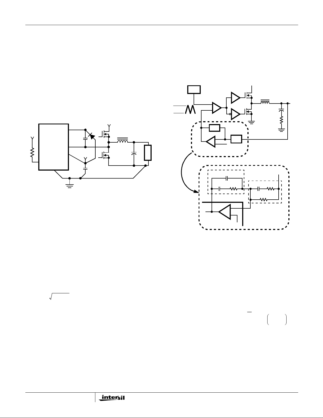
represent numerous physical capacitors. Locate the ISL6520
within 3 inches of the MOSFETs,Q
and Q2. The circuit traces
1
for the MOSFETs’gate and source connections from the
ISL6520 must be sized to handle up to 1A peak current.
Figure 4 shows the circuit traces that require additional layout
consideration. Use single point and ground plane construction
for the circuits shown. Minimize any leakage current paths on
the COMP/OCSETpin and locate the resistor,R
OSCET
close
to the COMP/OCSET pin because the internal current source is
only 20µA. Provide local V
GND pins. Locate the capacitor,C
decoupling between VCC and
CC
as close as practical to
BOOT
the BOOT and PHASE pins. All components used for feedback
compensation should be located as close to the IC a practical.
+V
IN
Q
L
1
O
C
Q
2
V
OUT
O
+5V
OCSET
R
ISL6520
COMP/OCSET
GND
BOOT
C
BOOT
PHASE
VCC
+5V
C
D
1
VCC
ISL6520
LOAD
ST
2. Place1
3. Place 2
4. Place 1
5. Place 2
Zero Below Filter’s Double Pole (~75% FLC).
ND
Zero at Filter’s Double Pole.
ST
Pole at the ESR Zero.
ND
Pole at Half the Switching Frequency.
6. Check Gain against Error Amplifier’s Open-Loop Gain.
7. Estimate Phase Margin - Repeat if Necessary.
V
∆V
OSC
OSC
PWM
COMPARATOR
-
+
Z
FB
V
E/A
-
+
ERROR
AMP
DETAILED COMPENSATION COMPONENTS
DRIVER
DRIVER
REFERENCE
C
2
C
R
1
Z
IN
2
PHASE
(PARASITIC)
Z
FB
C
IN
L
O
Z
IN
3
C
ESR
R
3
O
V
OUT
V
OUT
FIGURE 4. PRINTED CIRCUIT BOARD SMALL SIGNAL
LAYOUT GUIDELINES
Feedback Compensation
Figure 5 highlights the voltage-mode control loop for a
synchronous-rectified buck converter. The output voltage
(V
) is regulated to the Refer ence voltage level. The
OUT
error amplifier (Error Amp) output (V
) is compared with
E/A
the oscillator (OSC) triangular wave to provi de a pulsewidth modulat ed (PWM ) wave with an am pl i tude of V
IN
at
the PHASE node. The PWM wave is smoothed by the output
filter (L
and CO).
O
Modulator Break Frequency Equations
F
LC
1
----- ----------- ----------- ----------- ---- -=
2π xLOxC
F
O
ESR
The compensation network consistsof the error amplifier
(internalto the ISL6520) and the impedance networks Z
and ZFB. The goal of t he compensation network is to provide
a closed loop transfer function with the highest 0dB crossing
frequency(f
) and adequatephase margin. Phase margin
0dB
is the difference between the closed loop phase at f
180 degrees. The equations below relate the compensation
network’spoles, zeros and gain to the components (R
R
3,C1,C2
,andC3) in Figure 7. Use these guidelines for
locating the poles and zeros of the compensationnetwork:
1. Pick Gain (R
) for desired converter bandwidth.
2/R1
1
------ ----------- ----------- ----------- ---- -=
2π xESRxC
O
0dB
IN
and
1,R2
R
1
ISL6520
COMP
-
+
REFERENCE
FB
FIGURE 5. VOLTAGE-MODEBUCK CONVERTER
COMPENSATION DESIGN
The modulator transfer function is the small-signal transfer
function of V
OUT/VE/A
Gain and the output filter (L
break frequency at F
the modulator is simplythe input voltage(V
peak-to-peakoscillator voltage ∆V
. This function is dominated by a DC
and CO), with a double pole
O
andazeroatF
LC
OSC
. The DC Gain of
ESR
) divided by the
IN
.
Compensation Break Frequency Equations
F
Z1
F
Z2
1
------- ----------- ----------- ------ -=
2π xR
2xC1
------- ----------- ----------- ----------- ----------- ----=
2π xR
1
+()xC
1R3
F
------- ----------- ----------- ----------- ----------- ----- -=
P1
2π xR
------- ----------- ----------- ------ -=
F
P2
3
2π xR
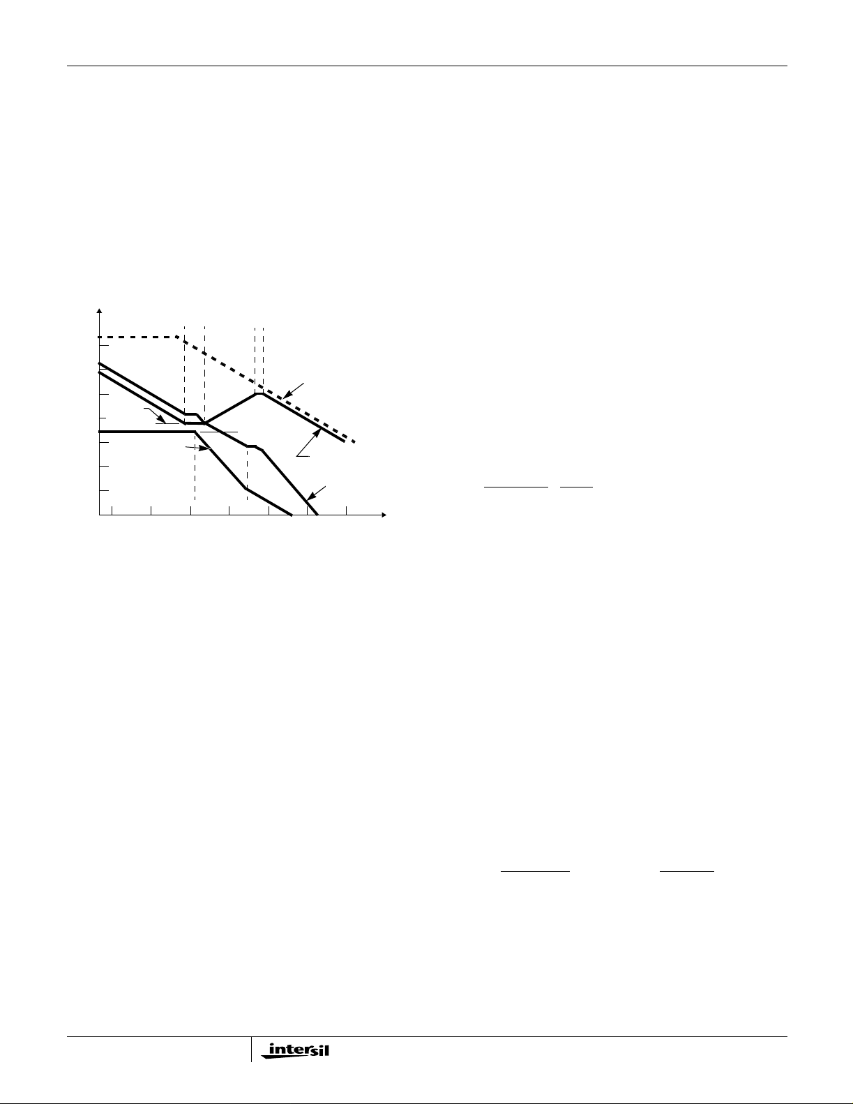
Figure 6 shows an asymptotic plot of the DC-DC converter’s
,
gain vs frequency. The actual Modulator Gain has a high gain
peak due to the high Q factor of the output filter and is not
shown in Figure 6. Using the above guidelines should give a
Compensation Gain similar to the curve plotted. The open
looperror amplifier gain bounds the compensation gain.
1
C
1xC2
------ ----------- ---- -
x
2
C1C2+
1
3xC3
6
Page 7
ISL6520
Check the compensation gain at FP2with the capabilities of
the error amplifier. The Closed Loop Gain is constructedon
the graph of Figure 6 by adding the Modulator Gain (in dB) to
the Compensation Gain (in dB). This is equivalent to
multiplying the modulator transfer function to the
compensationtransfer functionand plotting the gain.
The compensation gain uses external impedance networks
Z
and ZINto provide a stable,high bandwidth(BW) overall
FB
loop. A stable control loop has a gain crossing with
-20dB/decadeslope and a phase margin greater than 45
degrees. Include worst case component variations when
determiningphase margin.
100
80
60
40
20LOG
)
(R
20
2/R1
GAIN (dB)
0
MODULATOR
-20
-40
-60
FIGURE 6. ASYMPTOTIC BODE PLOT OF CONVERTER GAIN
GAIN
F
F
F
P1
Z2
Z1
F
LC
F
FREQUENCY (Hz)
(V
ESR
F
P2
OPEN LOOP
ERROR AMP GAIN
20LOG
/DV
IN
OSC
)
COMPENSATION
GAIN
CLOSEDLOOP
GAIN
10M1M100K10K1K10010
Use only specialized low-ESR capacitors intended for
switching-regulator applications for the bulk capacitors. The
bulk capacitor’s ESR will determine the output ripple voltage
and the initial voltage drop after a high slew-rate transient.
An aluminum electrolytic capacitor’s ESR value is related to
the case size with lower ESR available in larger case sizes.
However, the Equivalent Series Inductance (ESL) of these
capacitors increases with case size and can reduce the
usefulnessof the capacitor to high slew-rate t ransient
loading. Unfortunately, ESL is not a specified parameter.
Work with your capacitor supplier and m easure the
capacitor’s impedance with frequency to select a suitable
component.In most cases, multipleelectrolyticcapacitors of
small case size perform better than a single large case
capacitor.
Output Inductor Selection
The output inductor is selected to meet the output voltage
ripple requirements and minimize the converter’s response
time to t he load transient. The inductorvalue determines t he
converter’s ripple current and the ripple voltage is a function
of the ripple current. The ripple voltage and current are
approximatedby the following equations:
V
IN-VOUT
∆I =
FsxL
Increasingthe valueof inductancereduces the ripple current
and voltage. However, the large inductance values reduce
the converter’s response time to a load transient.
V
OUT
x
V
IN
∆V
OUT
= ∆IxESR
Component Selection Guidelines
Output Capacitor Selection
An output capacitor is requiredto filter the output and supply
the load transient current. The filtering requirements are a
function of the switching frequency and the ripple current.
The load transient requirements are a function of the slew
rate (di/dt)and t he magnitude of the transient load current.
These requirements are generally met with a mix of
capacitors and careful layout.
Modern components and loads are capable of producing
transient load rates above 1A/ns. High frequency capacitors
initially supplythe transient and slow the current load rate
seen by the bulk capacitors. The bulk filter capacitor values
are generallydetermined by the ESR (EffectiveSeries
Resistance) and voltageratingrequirementsratherthan
actual capacitance requirements.
High frequency decoupling capacitors should be placed as
closeto the power pins of the load as physically possible.Be
careful not to add inductance in the circuit board wiring that
could cancel t he usefulness of these low inductance
components. Consult with the manufacturer of the load on
specific decoupling requirements.
One of the parameters limiting t he converter’s res ponse to
a load transient is the time required to change t he inductor
current. Given a sufficiently f ast control loop design, the
ISL6520 will provide either 0% or 1 00% duty cycle i n
response to a load transient. The response time is the time
required t o slew the inductor cur rent from an initial cur rent
value to the transient current level. During this interval the
difference betw een the inductor current and the transient
current le vel must be supplied by the output capacitor.
Minimizing t he response time can minimize the output
capacitance re quire d.
The response time to a transient is different for the
applicationof load and the removal of load. The following
equations give the approximate response time interval for
applicationand removal of a transient load:
LxI
=
t
RISE
where: I
TRAN
VIN-V
OUT
is the transient load current step, t
TRAN
t
FALL
response time to the application of load, and t
LxI
TRAN
=
V
OUT
is the
RISE
is the
FALL
response time to the removal of load. The worst case
response time can be either at the application or removal of
load. Be sure to check both of these equations at the
7
Page 8
ISL6520
minimum and maximum output levels for the worst case
response time.
Input Capacitor Selection
Use a mix of input bypass capacitors to contro l the voltage
overshoot a cross the MOSFETs. U se small ceramic
capacitors for high frequency decoupling and bulk
capacitors to supply the current ne eded each time Q
1
turns
on. Place the small ceramic capacitors ph ysic ally close to
the MO SFETs and between the drain of Q
of Q
.
2
and the source
1
The important parameters for the bulk input capacitorare the
voltagerating and the RMS current rating. For reliable
operation, select the bulk capacitor with voltage and current
ratings above the maximum input voltage and largest RMS
current requiredby the circuit. The capacitorvoltage rating
should be at least 1.25 times greater than the maximum
input voltage and a voltage rating of 1.5 times is a
conservative guideline. The RMS current rating requirement
for the input capacitor of a buck regulator is approximately
1/2 the DC load current.
For a through hole design, several electrolytic capacitors
may be needed. For surface mount designs, solid tantalum
capacitors can be used, but caution must be exercised with
regard to the capacitor s urge current rating. These
capacitors must be capable of handling the surge-current at
power-up. Some capacitor series available from reputable
manufacturers are surge current tested.
MOSFET Selection/Considerations
The ISL6520 requires two N-Channel power MOSFETs.
These s houl d be selected based upon r
DS(ON)
supply requi rements, and thermal managem ent
requirements.
In high- cur rent applicat io ns, the MOSFET power
dissipation, package selection and heatsink are the
dominant design f actor s. The power dissipation includes
two loss componen ts; conduction loss and s witc hin g loss.
The condu ct ion losses are the largest co mponent of power
dissipation for both the upper an d the lower MOSFETs.
These losses are distributed between the two MOSFETs
according to duty factor (see t he equation s below). Only
the uppe r MOSFET has switching losses, since the lower
MOSFETs body diod e or an exter nal Schottky rectifier
across the lower MOSFET clamps the switching node
before the synchro nous rectifier turns on. These equati ons
assume l ine ar voltage-curren t transitions and do no t
adequately model power lo ss due the rever se-r ecovery of
the lower MOSF ET’s body diode. The gate- charge lo sses
are dissi pated by the IS L6520 and don't heat the
MOSFETs. However, large gate-charge increases t he
switching interval, t
which increases th e upper MOSFET
SW
switching l osses. Ensure that both MO SFETs are w i thin
their maxi mu m junction temperatur e at high a mbient
temperature by cal cul at ing the t emperature rise accor ding
,gate
to package thermal-resistance specificat i ons. A separate
heatsink may be necessary depending upon MOSFET
power, package type, ambient tem perat ur e and air f low.
1
P
P
Where: D is the duty cycle = V
UPPER
LOWER
=Io2xr
=Io2xr
t
is the switching interval, and
SW
F
is the switching frequency.
S
DS(ON)
DS(ON)
xD+
x(1-D)
Io x V
2
OUT/VIN
INxtSWxFS
,
Given the reduced available gate bias voltage (5V) ,
logic-level or sub-logic-l evel transisto rs should be used for
both N-M OSFETs. Caut io n should be exercised w i th
devices exhibiting very low V
GS(ON)
characteristics. The
shoot-through protection present aboard the ISL6520 may
be circumvented by these MOSFETs if th ey have large
parasitic impedences and/or capacitances that would
inhibit the gate of the MO SFET fr om being discharged
below its threshold level before the complementary
MOSFET is turned on.
+5V
VCC
ISL6520
-
+
FIGURE 7. UPPER GATE DRIVE BOOTSTRAP
D
+V
GND
BOOT
-
D
BOOT
UGATE
PHASE
LGATE
C
BOOT
Q1
Q2
+5V
NOTE:
V
G-S≈VCC-VD
NOTE:
V
G-S≈VCC
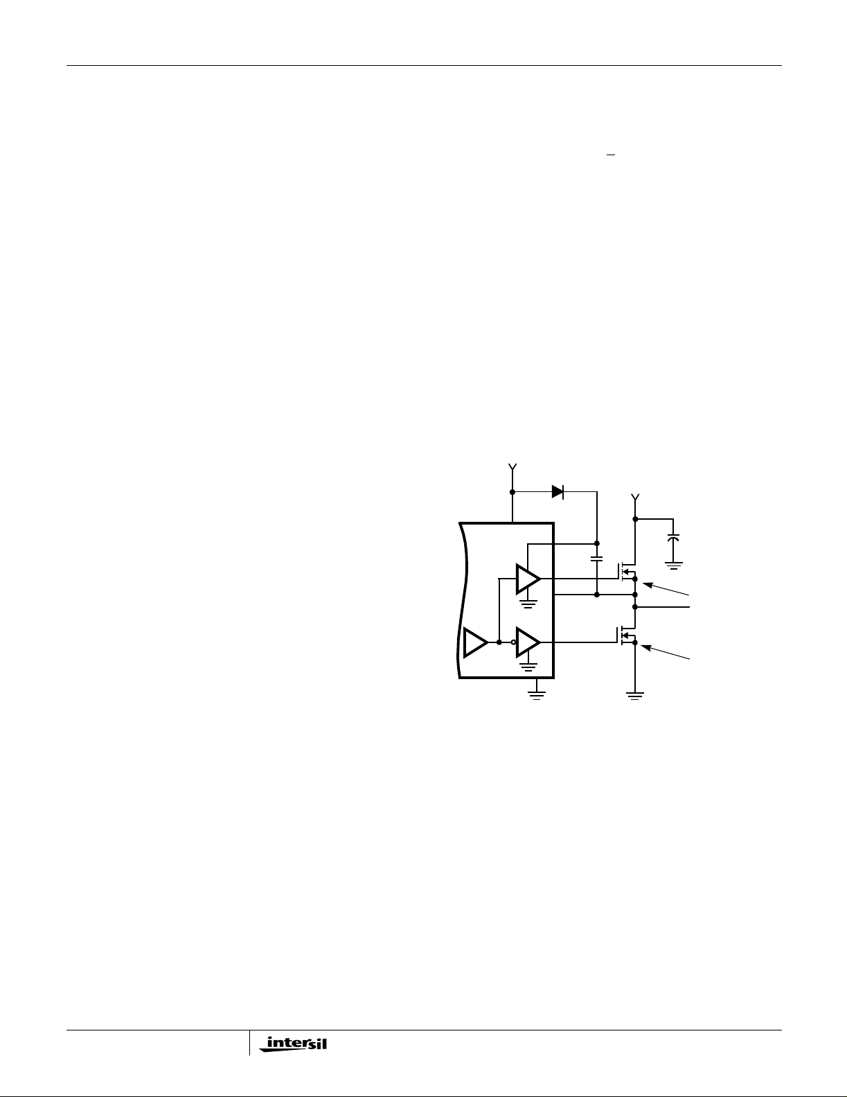
Figure 7 shows the upper gate drive (BOOT pin) supplied
by a bootstrap circuit fro m V
C
, develops a floating supply vo ltage reference d to
BOOT
the PHASE pin. The supply is refreshed to a voltage of V
. The boot capacitor,
CC
CC
less the boot diode drop (VD) each time the lower
MOSFET, Q
, turns on.
2
8
Page 9
ISL6520
ISL6520 DC-DC Converter Application Circuit
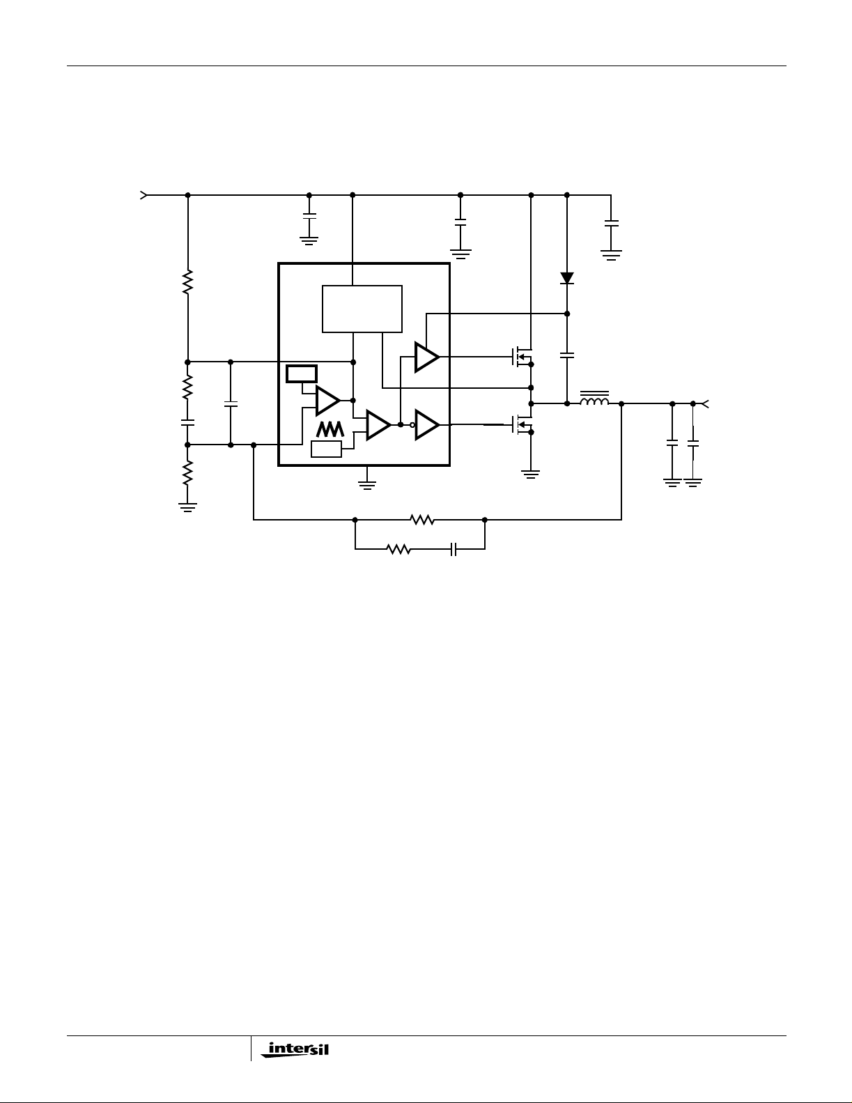
Figure 8 shows an a pplication circuit of a DC-DC Converter.
Detailed information on the circuit, including a complete Bill-
+5V
0.1µF
2 x 330µF
VCC
MONITOR
AND
PROTECTION
+
-
OSC
5
+
-
3
GND
6.19kΩ
10.0kΩ
8200pF
1.00kΩ
COMP/OCSET
470pF
FB
ISL6520
7
REF
6
U
1
of-Materials and circuit board description, can be found in
ApplicationNote AN9932.
+
C
IN
1
2
8
4
BOOT
UGATE
PHASE
LGATE
0.1µF
Q
1
Q
2
2x1µF
D
1
L
1
V
OUT
+
C
OUT
3 x 330µF
0.1µF
Component Selection Notes:
- Each 330mF 6.3WVDC, Sanyo 6TPB330M or Equivalent.
C
IN
C
- Each 330mF 6.3WVDC, Sanyo 6TPB330M or Equivalent.
OUT
D1 - 30mA Schottky Diode,MA732 or Equivalent
FIGURE 8. 5V to 3.3V 15A DC-DC CONVERTER
3.16kΩ
60.4Ω 18000pF
L
1
Q
1,Q2
-3.1µH Inductor,Panasonic P/N ETQ-P6F2ROLFAor Equivalent.
- Intersil MOSFET; HUF76143.
9
Page 10
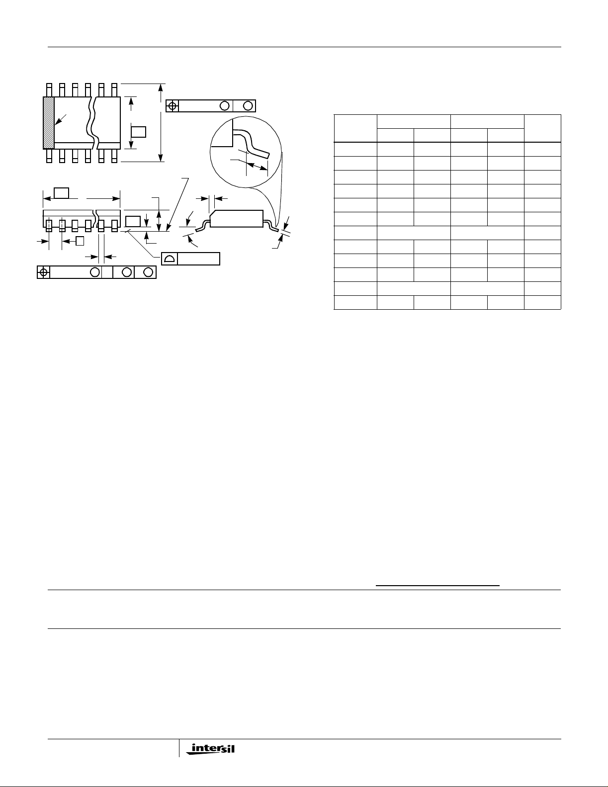
Small Outline Plastic Packages (SOIC)
ISL6520
N
INDEX
AREA
123
SEATING PLANE
-AD
e
B
0.25(0.010) C AM BS
E
-B-
A
-C-
M
0.25(0.010) BM M
H
α
µ
A1
0.10(0.004)
L
hx45
o
C
NOTES:
1. Symbolsaredefinedin the “MO SeriesSymbolList” in Section2.2 of
Publication Number 95.
2. Dimensioning and tolerancing per ANSI Y14.5M-1982.
3. Dimension“D” does not includemoldflash,protrusions or gate burrs.
Moldflash,protrusionandgateburrsshallnotexceed0.15mm(0.006
inch) per side.
4. Dimension“E” doesnot include interlead flash or protrusions. Interlead flash and protrusions shall not exceed 0.25mm (0.010 inch) per
side.
5. The chamfer on the body is optional. If it is not present, a visual index
feature must be located within the crosshatched area.
6. “L” is the length of terminal for soldering to a substrate.
7. “N” is the number of terminal positions.
8. Terminalnumbers are shown for reference only.
9. The lead width “B”, as measured 0.36mm (0.014 inch) or greater
above the seating plane, shall not exceed a maximum value of
0.61mm (0.024 inch).
10. Controllingdimension: MILLIMETER.Convertedinch dimensions
are not necessarily exact.
M8.15 (JEDEC MS-012-AA ISSUE C)
8 LEAD NARROW BODY SMALL OUTLINE PLASTIC
PACKAGE
INCHES M ILLIMETERS
SYMBOL
A 0.0532 0.0688 1.35 1.75 -
A1 0.0040 0.0098 0.10 0.25 -
B 0.013 0.020 0.33 0.51 9
C 0.0075 0.0098 0.19 0.25 D 0.1890 0.1968 4.80 5.00 3
E 0.1497 0.1574 3.80 4.00 4
e 0.050 BSC 1.27 BSC H 0.2284 0.2440 5.80 6.20 h 0.0099 0.0196 0.25 0.50 5
L 0.016 0.050 0.40 1.27 6
N8 87
o
α
0
o
8
o
0
o
8
Rev. 0 12/93
NOTESMIN MAX MIN MAX
-
All Intersil productsare manufactured, assembled and tested utilizing ISO9000 quality systems.
Intersil Corporation’s quality certifications can be viewed at website www.intersil.com/design/quality
Intersil products are sold by description only. Intersil Corporation reserves the right to make changes in circuit design and/or specifications at any time without notice.
Accordingly, the reader is cautionedto verify that data sheets are current before placing orders. Information furnished by Intersil is believed to be accurate and reliable.However,no responsibilityis assumed by Intersil or its subsidiaries for its use; nor for any infringementsof patentsor other rights of thirdpartieswhich may result from its use. No
license is granted by implication or otherwise under any patent or patent rights of Intersil or its subsidiaries.
For information regarding Intersil Corporation and its products, see web site www.intersil.com
Sales Office Headquarters
NORTH AMERICA
Intersil Corporation
2401 Palm Bay Rd.
Palm Bay, FL 32905
TEL: (321) 724-7000
FAX: (321) 724-7240
EUROPE
Intersil SA
MercureCenter
100,RuedelaFusee
1130 Brussels, Belgium
TEL: (32) 2.724.2111
FAX: (32) 2.724.22.05
10
ASIA
Intersil Ltd.
8F-2,96, Sec. 1, Chien-kuo North,
Taipei, Taiwan 104
Republic of China
TEL: 886-2-2515-8508
FAX: 886-2-2515-8369
 Loading...