

Page 1

DATASHEET
ISL6420
Advanced Single Synchronous Buck Pulse-Width Modulation (PWM) Controller
The ISL6420 makes simple work out of implementing a
complete control and protection scheme for a highperformance DC/DC buck converter. Designed to drive
N-channel MOSFETs in a synchronous rectified buck
topology, the ISL6420 integrates control, output adjustment,
monitoring and protection functions into a single package.
Additionally, the IC features an external reference voltage
tracking mode for externally referenced buck converter
applications and DDR termination supplies, as well as a
voltage margining mode for system testing in networking
DC/DC converter applications.
The ISL6420 provides simple, single feedback loop, voltage
mode control with fast transient response. The output
voltage of the converter can be precisely regulated to as low
as 0.6V.
The operating frequency is fully adjustable from 100kHz to
1.4MHz. High frequency operation offers cost and space
savings.
The error amplifier features a 15MHz gain-bandwidth
product and 6V/µs slew rate that enables high converter
bandwidth for fast transient response. The PWM duty cycle
ranges from 0% to 100% in transient conditions. Selecting
the capacitor value from the ENSS pin to ground sets a fully
adjustable PWM soft-start. Pulling the ENSS pin LOW
disables the controller.
The ISL6420 monitors the output voltage and generates a
PGOOD (power good) signal when soft-start sequence is
complete and the output is within regulation. A built-in
overvoltage protection circuit prevents the output voltage
from going above typically 115% of the set point. Protection
from overcurrent conditions is provided by monitoring the
r
appropriately. This approach simplifies the implementation
and improves efficiency by eliminating the need for a current
sensing resistor.
of the upper MOSFET to inhibit the PWM operation
DS(ON)
Features
• Operates from 4.5V to 16V Input
• 0.6V Internal Reference Voltage
- ±1.0% Reference Voltage Accuracy
• Resistor-Selectable Switching Frequency
- 100kHz to 1.4MHz
• Voltage Margining and External Reference Tracking
Modes
• Output Can Sink or Source Current
• Lossless, Programmable Overcurrent Protection
- Uses Upper MOSFET‘s r
• Programmable Soft-Start
• Drives N-Channel MOSFETs
• Simple Single-Loop Control Design
- Voltage-Mode PWM Control
• Fast Transient Response
- High-Bandwidth Error Amplifier
- Full 0% to 100% Duty Cycle
• Extensive Circuit Protection Functions
- PGOOD, overvoltage, overcurrent, Shutdown
• QFN (4x4) Package
- QFN Compliant to JEDEC PUB95 MO-220 QFN - Quad
Flat No Leads - Product Outline
- QFN Near Chip Scale Package Footprint; Improves
PCB Efficiency, Thinner in Profile
• Also Available in QSOP Package
• Pb-Free Available (RoHS Compliant)
Applications
• Power Supplies for Microprocessors/ASICs
- Embedded Controllers
- DSP and Core Processors
- DDR SDRAM Bus Termination
• Ethernet Routers and Switchers
• High-Power DC/DC Regulators
FN9151
Rev 5.00
Feb 13, 2008
DS(ON)
• Distributed DC/DC Power Architecture
• Personal Computer Peripherals
• Externally Referenced Buck Converters
FN9151 Rev 5.00 Page 1 of 20
Feb 13, 2008
Page 2
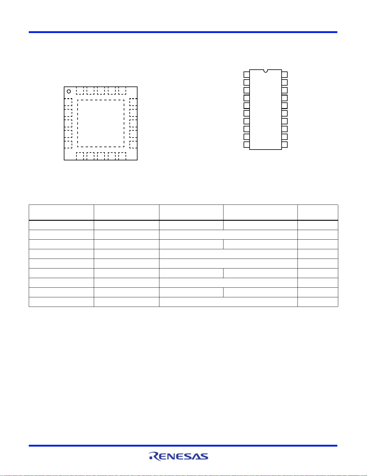
ISL6420
GPIO2
GPIO1/REFIN
OCSET
VMSET/MODE
BOOT
UGATE
PHASE
PVCC
LGATE
VIN
SGND
RT
FB
REFOUT
VCC5
1
2
3
4
5
678910
15
14
13
12
11
20 19 18 17 16
PGND
CDEL
PGOOD
ENSS
COMP
11
12
13
14
15
16
17
18
20
19
10
9
8
7
6
5
4
3
2
1
CDEL
PGND
LGATE
PVCC
PHASE
UGATE
GPIO2
BOOT
GPIO1/REFIN
OCSET
PGOOD
COMP
FB
RT
ENSS
SGND
VIN
VCC5
VMSET/MODE
REFOUT
Pinouts
ISL6420
(20 LD QFN)
TOP VIEW
Ordering Information
ISL6420
(20 LD QSOP)
TOP VIEW
FN9151 Rev 5.00 Page 2 of 20
Feb 13, 2008
PART NUMBER PART MARKING
TEMP.
RANGE (°C) PACKAGE
PKG.
DWG. #
ISL6420IR ISL 6420IRZ -40 to +85 20 Ld 4x4 QFN L20.4x4
ISL6420IR-T* ISL 6420IRZ 20 Ld 4x4 QFN Tape and Reel L20.4x4
ISL6420IRZ (Note) 64 20IRZ -40 to +85 20 Ld 4x4 QFN (Pb-free) L20.4x4
ISL6420IRZ-T* (Note) 64 20IRZ 20 Ld 4x4 QFN Tape and Reel (Pb-free) L20.4x4
ISL6420IRZ-TK* (Note) 64 20IRZ 20 Ld 4x4 QFN Tape and Reel (Pb-free) L20.4x4
ISL6420IA ISL 6420IA -40 to +85 20 Ld QSOP M20.15
ISL6420IA-TK* ISL 6420IA 20 Ld QSOP Tape and Reel M20.15
ISL6420IAZ (Note) ISL 6420IAZ -40 to +85 20 Ld QSOP (Pb-free) M20.15
ISL6420IAZ-TK* (Note) ISL 6420IAZ 20 Ld QSOP Tape and Reel (Pb-free) M20.15
*Please refer to TB347 for details on reel specifications.
NOTE: These Intersil Pb-free plastic packaged products employ special Pb-free material sets; molding compounds/die attach materials and 100%
matte tin plate PLUS ANNEAL - e3 termination finish, which is RoHS compliant and compatible with both SnPb and Pb-free soldering operations.
Intersil Pb-free products are MSL classified at Pb-free peak reflow temperatures that meet or exceed the Pb-free requirements of IPC/JEDEC J
STD-020.
Page 3
ISL6420
GENERATOR
PWM
COMP
ERROR
AMP
VIN
VMSET/MODE
PGND
OCSET
GPIO2
REFOUT
PHASE
LOGIC
BOOT
UGATE
LGATE
PHASE
REFERENCE
+
-
+
-
VOLTAGE
MARGINING
GPIO1/REFIN
0.6V
OV/UV
VOLTAGE
MONITOR
RAMP
PVCC
PWM
LOGIC
OSC
EN/SS
UVFLT
OVFLT
UVFLT
OVFLT
OCFLT
FAULT
LOGIC
FB
COMP
FB
ENSS
RT
LDO
VCC5
+
-
PHASE
OVERCURRENT
COMP
SGND
SS
CDEL
PGOOD
RT
FB
COMP
ENSS
REF
-
+
+
-
OSC
VIN
5V
C1
L1
C10
0.1µF
UGATE
OCSET
PHASE
BOOT
D1
Q1
C7
R2
R4
C12
C11
C2
C6
C5
R1
C9
LGATE
Q2
3.3V
R3
MONITOR AND
PROTECTION
+
-
+
-
GPIO1/REFIN
GPIO2
REFOUT
VMSET/MODE
CDEL
PGND
PVCC
SGND
VCC5
C4
C3
PGOOD
R5
C8
R6
C13
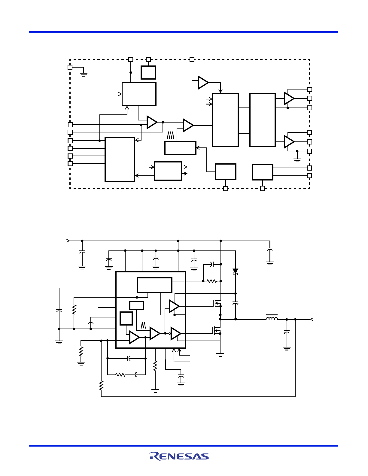
Functional Block Diagram
Typical 5V Input DC/DC Application Schematic
FN9151 Rev 5.00 Page 3 of 20
Feb 13, 2008
Page 4
ISL6420
RT
FB
COMP
ENSS
REF
-
+
+
-
OSC
VIN
12V
C1
L1
C10
UGATE
OCSET
PHASE
BOOT
D1
Q1
C7
R2
R4
C12
C11
C2
C6
C5
R1
C9
LGATE
Q2
3.3V
R3
MONITOR AND
PROTECTION
+
-
+
-
GPIO1/REFIN
GPIO2
VMSET/MODE
PGND
PVCC
SGND
VCC5
C4
C3
PGOOD
CDEL
R5
C8
R6
REFOUT
C13
RT
FB
COMP
SS/EN
REF
-
+
+
-
OSC
VIN
5V
C1
L1
C9
UGATE
OCSET
PHASE
BOOT
D1
Q1
C7
R2
R4
C11
R5
C10
C2
C6
C5
R1
C8
LGATE
Q2
2.5V/1.25V
R3
MONITOR AND
PROTECTION
+
-
+
-
GPIO2
VMSET/MODE
CDEL
PGND
PVCC
SGND
VCC5
C4
C3
PGOOD
CONFIGURATION FOR DDR TERMINATION/EXTERNALLY REFERENCED TRACKING APPLICATIONS
VCC5
C12
REFOUT
1.25V VREF
TO REFIN OF VTT SUPPLY
GPIO1/REFIN <-- VREF = VDDQ/2
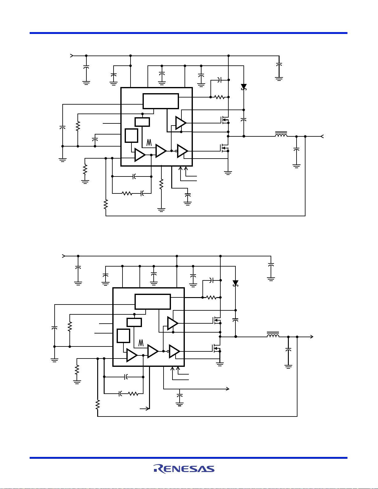
Typical 12V Input DC/DC Application Schematic
Typical 5V Input DC/DC Application Schematic
FN9151 Rev 5.00 Page 4 of 20
Feb 13, 2008
Page 5
ISL6420
RT
FB
COMP
SS/EN
REF
-
+
+
-
OSC
VIN
12V
C1
L1
C9
UGATE
OCSET
PHASE
BOOT
D1
Q1
C7
R2
R4
C11
R5
C10
C2
C6
C5
R1
C8
LGATE
Q2
2.5V/1.25V
R3
MONITOR AND
PROTECTION
+
-
+
-
GPIO1/REFIN <-- VREF = VDDQ/2
GPIO2
VMSET/MODE
CDEL
PGND
PVCC
SGND
VCC5
C4
C3
PGOOD
CONFIGURATION FOR DDR TERMINATION/EXTERNALLY REFERENCED TRACKING APPLICATIONS
VCC5
C12
REFOUT
1.25V VREF
VDDQ/VTT
TO REFIN OF VTT SUPPLY
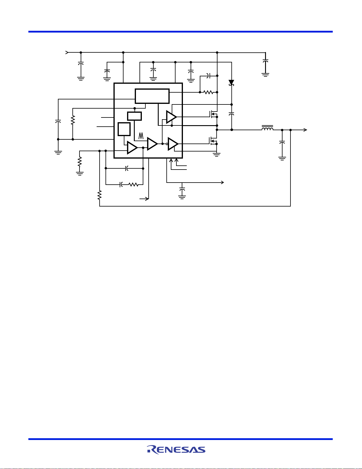
Typical 12V Input DC/DC Application Schematic
FN9151 Rev 5.00 Page 5 of 20
Feb 13, 2008
Page 6
ISL6420
Absolute Maximum Ratings (Note 1) Thermal Information
Bias Voltage, VIN . . . . . . . . . . . . . . . . . . . . . . . . . . . . . . . . . . . .+18V
BOOT and Ugate Pins . . . . . . . . . . . . . . . . . . . . . . . . . . . . . . . . . . +24V
CAUTION: Do not operate at or near the maximum ratings listed for extended periods of time. Exposure to such conditions may adversely impact product reliability and
result in failures not covered by warranty.
NOTES:
1. All voltages are with respect to GND.
is measured in free air with the component mounted on a high effective thermal conductivity test board with “direct attach” features. See
2.
JA
Tech Brief TB379.
3. For
, the “case temp” location is the center of the exposed metal pad on the package underside.
JC
Thermal Resistance (Typical) JA (°C/W) JC (°C/W)
QFN Package (Notes 2, 3). . . . . . . . . . 47 8.5
QSOP Package (Note 2) . . . . . . . . . . . 90 NA
Maximum Junction Temperature (Plastic Package) . . . . . . . +150°C
Maximum Storage Temperature Range . . . . . . . . . . -65°C to +150°C
Ambient Temperature Range . . . . . . . . -40°C to +85°C (for “I” suffix)
Junction Temperature Range. . . . . . . . . . . . . . . . . .-40°C to +125°C
Pb-free reflow profile . . . . . . . . . . . . . . . . . . . . . . . . . .see link below
http://www.intersil.com/pbfree/Pb-FreeReflow.asp
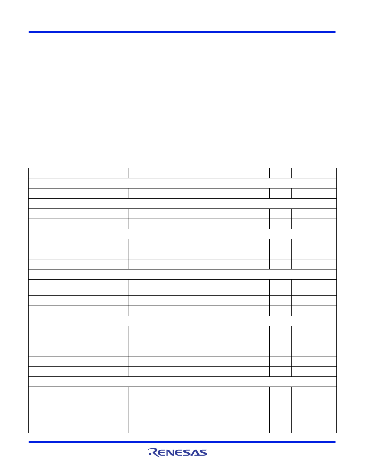
Electrical Specifications Operating Conditions, Unless Otherwise Noted: VIN = 12V, PV
shorted with V
CC
, TA = +25°C
CC5
PARAMETER SYMBOL TEST CONDITIONS MIN TYP MAX UNITS
VIN SUPPLY
Input Voltage Range 5.6 12 16 V
VIN SUPPLY CURRENT
Shutdown Current (Note 4) ENSS = GND - 1.4 - mA
Operating Current (Notes 4, 5) -2.03.0mA
VCC5 SUPPLY (Notes 5, 6)
Input Voltage Range VIN = VCC5 for 5V configuration 4.5 5.0 5.5 V
Output Voltage VIN = 5.6V to 16V, I
= 3mA to 50mA 4.5 5.0 5.5 V
L
Maximum Output Current VIN = 12V 50 - - mA
POWER-ON RESET
Rising V
Falling V
Threshold VIN connected to VCC5, 5V input
CC5
Threshold 4.09 4.1 4.25 V
CC5
operation
4.32 4.4 4.45 V
UVLO Threshold Hysteresis 0.16 - - V
PWM CONVERTERS
Maximum Duty Cycle F
Minimum Duty Cycle F
= 300kHz 90 96 - %
SW
= 300kHz - - 0 %
SW
FB pin bias current -80-nA
Undervoltage Protection V
Overvoltage Protection V
UV1
OVP1
Fraction of the set point; ~3s noise filter 75 - 85 %
Fraction of the set point; ~1s noise filter 112 - 120 %
OSCILLATOR
Free Running Frequency RT = VCC5, T
Total Variation T
= -40°C to +85°C, with freq. set by
A
external resistor at RT
= -40°C to +85°C 270 300 330 kHz
A
-10 - +10 %
Frequency Range (Set by RT) VIN = 12V 100 - 1400 kHz
Ramp Amplitude (Note 7) V
OSC
-1.25-V
FN9151 Rev 5.00 Page 6 of 20
Feb 13, 2008
P-P
Page 7
ISL6420
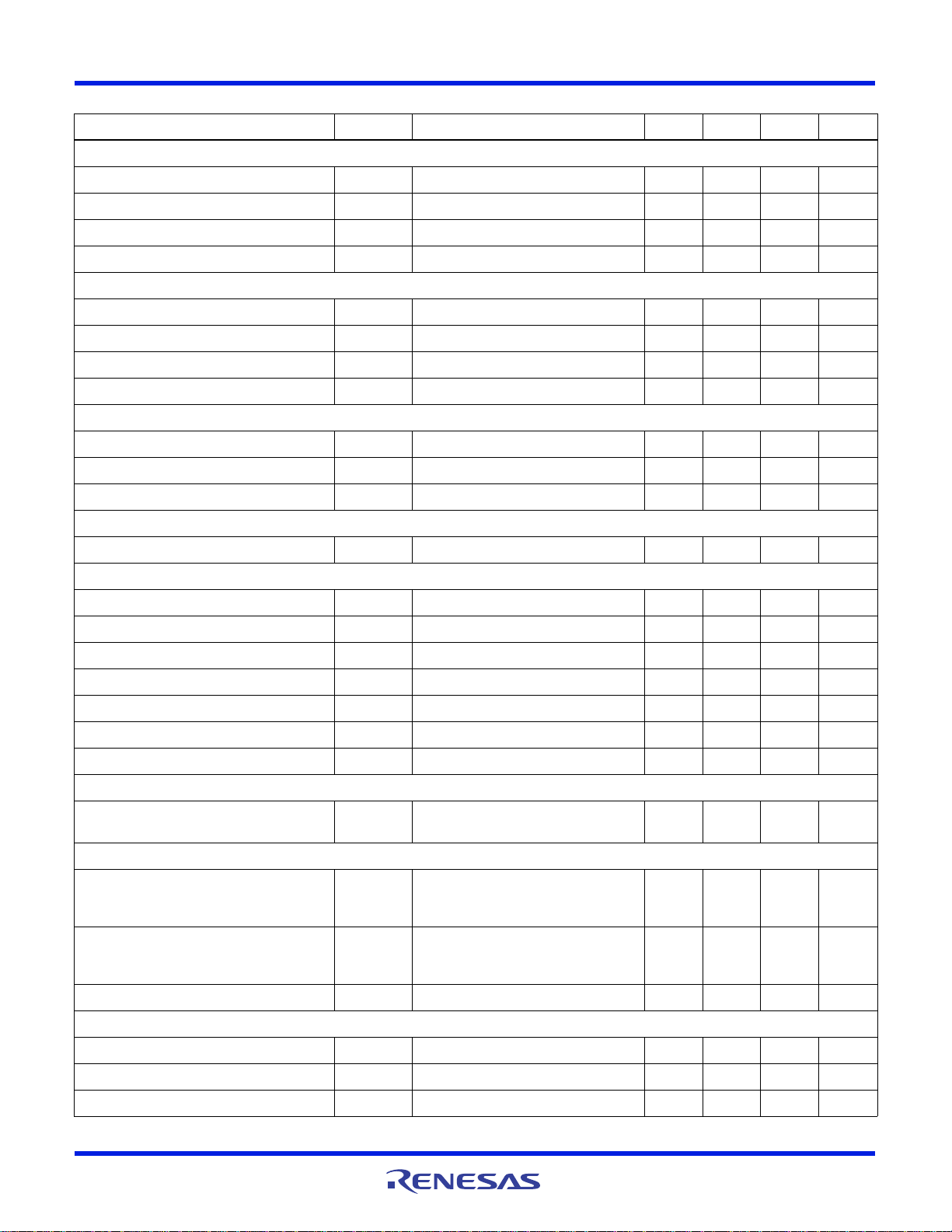
Electrical Specifications Operating Conditions, Unless Otherwise Noted: VIN = 12V, PV
shorted with V
CC
, TA = +25°C (Continued)
CC5
PARAMETER SYMBOL TEST CONDITIONS MIN TYP MAX UNITS
REFERENCE AND SOFT-START/ENABLE
Internal Reference Voltage V
Soft-Start Current I
Soft-Start Threshold V
REF
SS
SOFT
0.594 0.606 V
-10-A
1.0 - - V
Enable Low (Converter disabled) --1.0V
PWM CONTROLLER GATE DRIVERS
Gate Drive Peak Current -0.7- A
Rise Time Co = 1000pF - 20 - ns
Fall Time Co = 1000pF - 20 - ns
Dead Time Between Drivers -20-ns
ERROR AMPLIFIER
DC Gain (Note 7) -88-dB
Gain-Bandwidth Product (Note 7) GBW - 15 - MHz
Slew Rate (Note 7) SR - 6 - V/s
PROTECTION
OCSET Current Source I
OCSET
Vocset = 4.5V 80 100 120 A
POWER GOOD AND CONTROL FUNCTIONS
Power-Good Lower Threshold V
Power-Good Higher Threshold V
PGOOD Leakage Current I
PG-
PG+
PGLKGVPULLUP
PGOOD Voltage Low I
Fraction of the set point; ~3s noise filter -14 -10 -8 %
Fraction of the set point; ~3s noise filter 10 - 16 %
= 5.5V - - 1 A
= 4mA - - 0.5 V
PGOOD
PGOOD Delay CDEL = 0.1µF - 125 - ms
CDEL Current for PGOOD CDEL threshold = 2.5V - 2 - A
CDEL Threshold -2.5- V
EXTERNAL REFERENCE
External Reference Input Range at
VMSET/MODE = H, C
= 2.2µF 0.6 - 1.25 V
REFOUT
GPIO1/REFIN.
REFERENCE BUFFER
Buffered Output Voltage - Internal Reference V
Buffered Output Voltage - External Reference V
REFOUTIREFOUT
REFOUTVREFIN
Current Drive Capability C
= 20mA,
VMSET/MODE = HIGH,
C
REFOUT
= 2.2µF, TA = -40°C to +85°C
= 1.25V, I
REFOUT
VMSET/MODE = HIGH,
C
REFOUT
REFOUT
= 2.2µF
= 2.2µF 20 - - mA
= 20mA,
0.585 0.6V 0.615 V
Vrefin
-0.01
-Vrefin
+0.01
V
VOLTAGE MARGINING
Voltage Margining Range (Note 7) -10 +10 %
CDEL Current for Voltage Margining - 100 - A
Slew Time CDEL = 0.1µF, VMSET/MODE = 330k -2.5- ms
FN9151 Rev 5.00 Page 7 of 20
Feb 13, 2008
Page 8
ISL6420
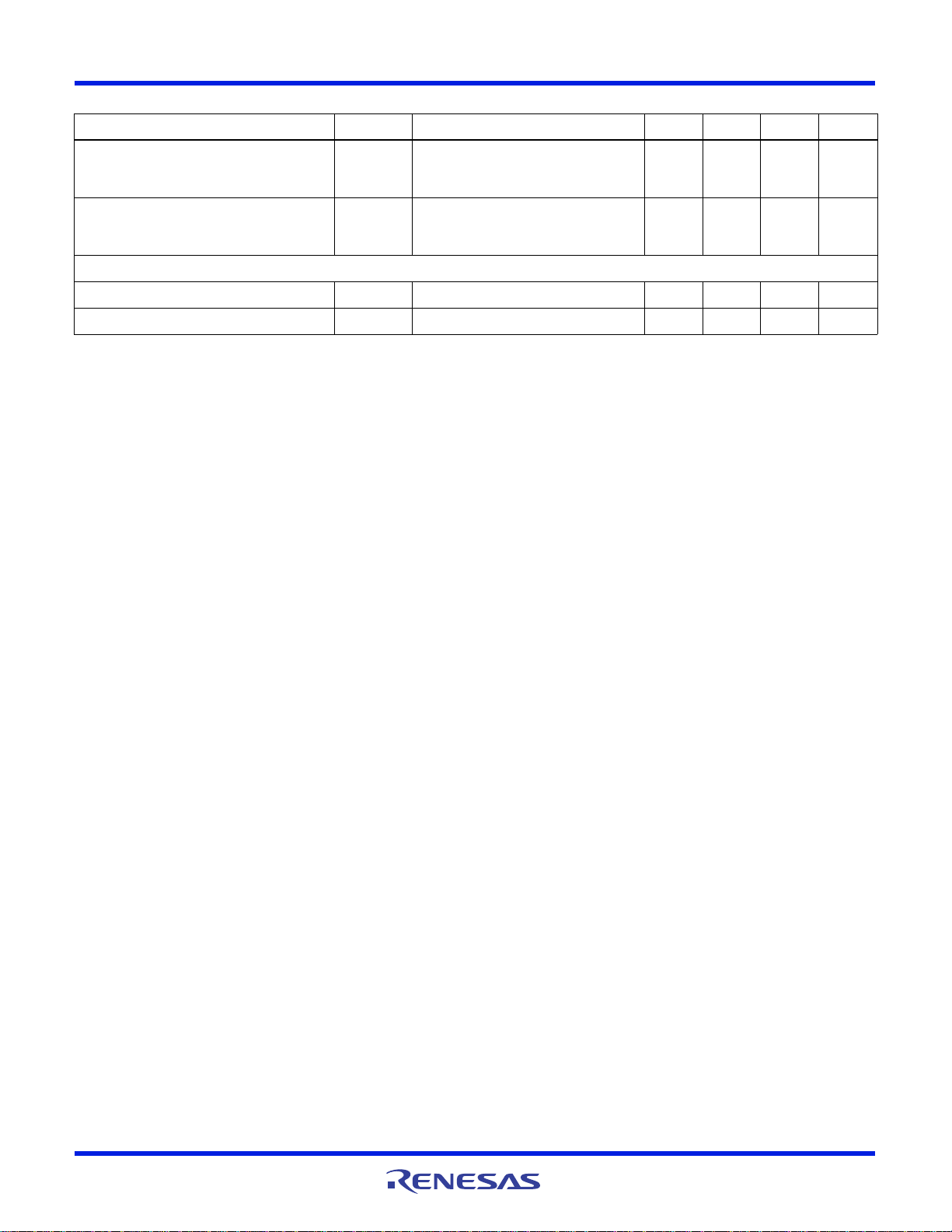
Electrical Specifications Operating Conditions, Unless Otherwise Noted: VIN = 12V, PV
PARAMETER SYMBOL TEST CONDITIONS MIN TYP MAX UNITS
ISET1 on FB Pin VMSET/MODE = 330k,
GPIO1/REFIN = L
GPIO2 = H
ISET2 on FB Pin VMSET/MODE = 330k,
GPIO1/REFIN = H
GPIO2 = L
THERMAL SHUTDOWN
Shutdown Temperature (Note 7) - 150 - °C
Thermal Shutdown Hysteresis (Note 7) - 20 - °C
NOTES:
4. The operating supply current and shutdown current specifications for 5V input are the same as VIN supply current specifications, i.e., 5.6V to
16V input conditions. These should also be tested with part configured for 5V input configuration, i.e., VIN = VCC5 = PVCC = 5V.
5. This is the V
6. When the input voltage is 5.6V to 16V at VIN pin, the VCC5 pin provides a 5V output capable of 50mA (max) total from the internal LDO. When
the input voltage is 5V, VCC5 pin will be used as a 5V input, the internal LDO regulator is disabled and the VIN must be connected to the VCC5.
In both cases the PVCC pin should always be connected to VCC5 pin. (Refer to the Pin Descriptions sections for more details.)
7. Limits established by characterization and are not production tested.
current consumed when the device is active but not switching. Does not include gate drive current.
CC
shorted with V
CC
, TA = +25°C (Continued)
CC5
-7.48- A
-7.48- A
FN9151 Rev 5.00 Page 8 of 20
Feb 13, 2008
Page 9
ISL6420
0.604
0.602
0.6
0.598
0.596
0.594
-40 60-15 10 35 85
TEMPERATURE (°C)
VREF (V)
320
310
300
290
280
270
-40 60-15 10 35 85
TEMPERATURE (°C)
V
SW
(kHz)
1.15
1.05
0.95
0.85
-40 60-15 10 35 85
TEMPERATURE (°C)
I
OCSET
NORMALIZED
80
82
84
86
88
90
92
94
96
98
0123 456 78 910
LOAD (A)
EFFICIENCY (%)
V
IN
= 12V
V
IN
= 5V
Typical Performance Curves
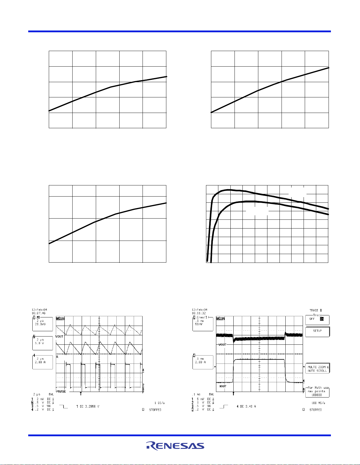
FIGURE 1. VREF vs. TEMPERATURE FIGURE 2. VSW vs. TEMPERATURE
FIGURE 3. IOCSET vs. TEMPERATURE FIGURE 4. EFFICIENCY vs. LOAD CURRENT (VOUT = 3.3V)
FN9151 Rev 5.00 Page 9 of 20
Feb 13, 2008
FIGURE 5. PWM WAVEFORMS FIGURE 6. LOAD TRANSIENT RESPONSE
Page 10
ISL6420
0
100
200
300
400
500
600
700
800
900
1000
1100
1200
1300
1400
0 25 50 75 100 125 150
RT (k)
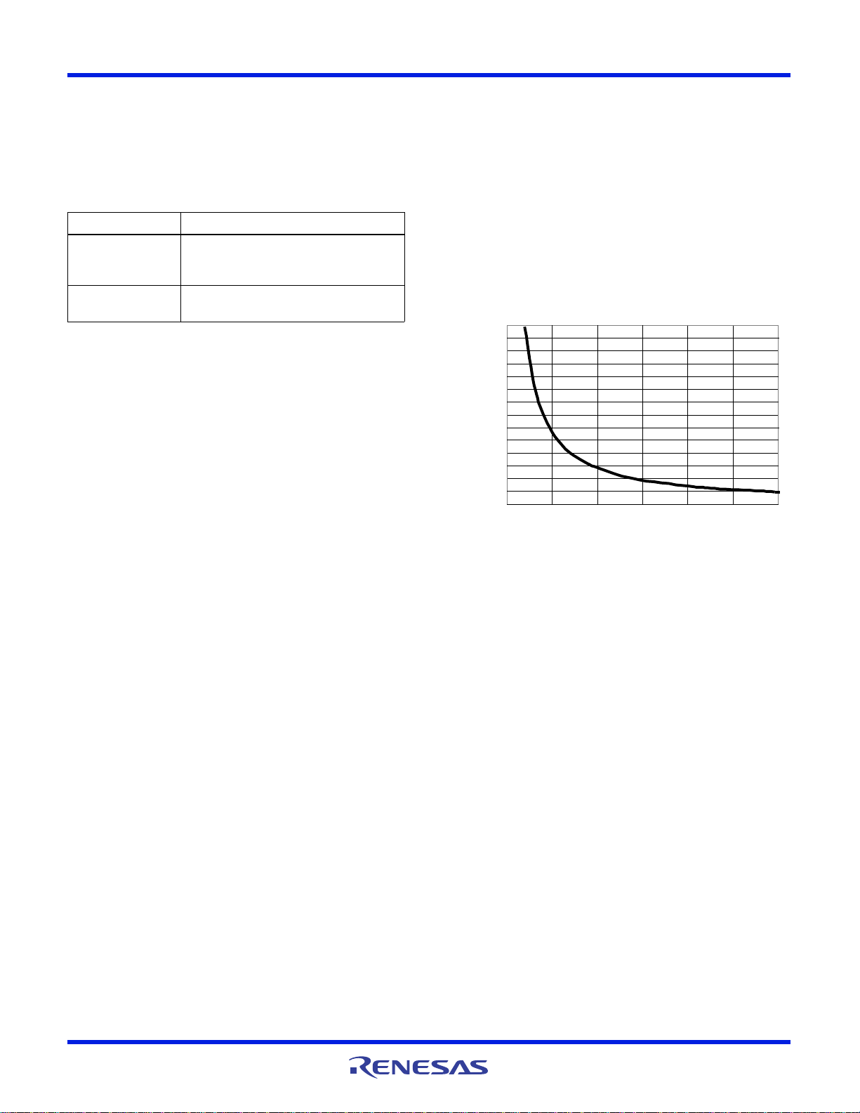
FREQUENCY (kHz)
FIGURE 7. OSCILLATOR FREQUENCY vs. RT
Pin Descriptions
VIN
This pin powers the controller and must be closely
decoupled to ground using a ceramic capacitor as close to
the VIN pin as possible.
TABLE 1. INPUT SUPPLY CONFIGURATION
INPUT PIN CONFIGURATION
5.6V to 16V Connect the input to the VIN pin. The VCC5
pin will provide a 5V output from the internal
LDO. Connect PVCC to VCC5.
5V +±10% Connect the input to the VCC5 pin. Connect
the PVCC and VIN pins to VCC5.
SGND
This pin provides the signal and power ground for the IC. Tie
this pin to the ground plane through the lowest impedance
connection.
LGATE
This pin provides the PWM-controlled gate drive for the
lower MOSFET.
PHASE
This pin is the junction point of the output filter inductor, the
upper MOSFET source and the lower MOSFET drain. This
pin is used to monitor the voltage drop across the upper
MOSFET for overcurrent protection. This pin also provides a
return path for the upper gate drive.
UGATE
This pin provides the PWM-controlled gate drive for the
upper MOSFET.
BOOT
This pin powers the upper MOSFET driver. Connect this pin
to the junction of the bootstrap capacitor and the cathode of
the bootstrap diode. The anode of the bootstrap diode is
connected to the VCC5 pin.
FB
This pin is connected to the feedback resistor divider and
provides the voltage feedback signal for the controller. This
pin sets the output voltage of the converter.
COMP
This pin is the error amplifier output pin. It is used as the
compensation point for the PWM error amplifier.
PGOOD
This pin provides a power good status. It is an open collector
output used to indicate the status of the output voltage.
RT
This is the oscillator frequency selection pin. Connecting this
pin directly to VCC5 will select the oscillator free running
FN9151 Rev 5.00 Page 10 of 20
Feb 13, 2008
frequency of 300kHz. By placing a resistor from this pin to
GND, the oscillator frequency can be programmed from
100kHz to 1.4MHz. Figure 7 shows the oscillator frequency
vs. the RT resistance.
CDEL
The PGOOD signal can be delayed by a time proportional to
a CDEL current of 2µA and the value of the capacitor
connected between this pin and ground. A 0.1µF will
typically provide 125ms delay. When in the Voltage
Margining mode the CDEL current is 100µA typical and
provides the delay for the output voltage slew rate, 2.5ms
typical for the 0.1µF capacitor.
PGND
This pin provides the power ground for the IC. Tie this pin to
the ground plane through the lowest impedance connection.
PVCC
This pin is the power connection for the gate drivers.
Connect this pin to the VCC5 pin.
VCC5
This pin is the output of the internal 5V LDO. Connect a
minimum of 4.7µF ceramic decoupling capacitor as close to
the IC as possible at this pin. Refer to Table 1.
ENSS
This pin provides enable/disable function and soft-start for
the PWM output. The output drivers are turned off when this
pin is held below 1V.
OCSET
Connect a resistor (R
the drain of the upper MOSFET. R
current source (I
resistance r
OCSET
set the converter overcurrent (OC) trip
DS(ON)
point.
) and a capacitor from this pin to
OCSET
, an internal 100µA
OCSET
), and the upper MOSFET on
Page 11
ISL6420
GPIO1/REFIN
This is a dual function pin. If VMSET/MODE is not connected
to VCC5 then this pin serves as GPIO1. Refer to Table 2 for
GPIO1 commands interpretation.
If VMSET/MODE is connected to VCC5 then this pin will
serve as REFIN. As REFIN, this pin is the non-inverting input
to the error amplifier. Connect the desired reference voltage
to this pin in the range of 0.6V to 1.25V.
Connect this pin to VCC5 to use internal reference.
REFOUT
It provides buffered reference output for REFIN. Connect
2.2µF decoupling capacitor to this pin.
VMSET/MODE
This pin is a dual function pin. Tie this pin to VCC5 to disable
voltage margining. When not tied to VCC5, this pin serves as
VMSET. Connect a resistor from this pin to ground to set the
delta for voltage margining. If voltage margining and external
TABLE 3. VOLTAGE MARGINING/DDR OR TRACKING SUPPLY PIN CONFIGURATION
FUNCTION/MODES
VMSET/MODE REFOUT GPIO1/REFIN GPIO2
reference tracking mode are not needed, this pin can be tied
directly to ground.
GPIO2
This is general purpose IO pin for voltage margining. Refer
to Table 2.
Exposed Thermal Pad
This pad is electrically isolated. Connect this pad to the
signal ground plane using at least five vias for a robust
thermal conduction path.
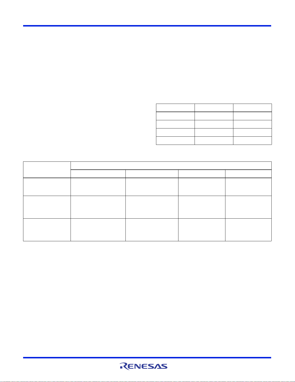
TABLE 2. VOLTAGE MARGINING CONTROLLED BY
GPIO1/REFIN AND GPIO2
GPIO1/REFIN GPIO2 VOUT
L L No Change
LH+ Delta VOUT
H L - Delta VOUT
H H Ignored
PIN CONFIGURATIONS
Enable Voltage Margining Pin Connected to GND with
No Voltage Margining.
Normal operation with
internal reference.
Buffered V
No Voltage Margining.
External reference.
Buffered V
V
REFIN
NOTES:
8. The GPIO1/REFIN and GPIO2 pins cannot be left floating.
9. Ensure that GPIO1/REFIN is tied high prior to the logic change at VMSET/MODE.
REFOUT
REFOUT
= 0.6V.
=
resistor. It is used as VMSET.
H Connect a 2.2µF capacitor to
H Connect a 2.2µF capacitor to
Connect a 2.2µF capacitor for
bypass of external reference.
GND.
GND.
Serves as a general
purpose I/O. Refer to
Table 2
H (Note 9) L
Connect to an external
reference voltage source
(0.6V to 1.25V)
Serves as a general
purpose I/O. Refer to
Table 2
L
FN9151 Rev 5.00 Page 11 of 20
Feb 13, 2008
Page 12
ISL6420
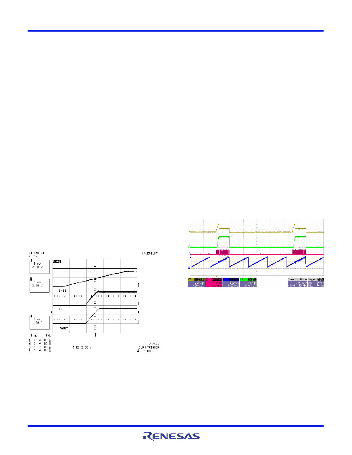
FIGURE 8. TYPICAL SOFT-START WAVEFORM
FIGURE 9. TYPICAL OVER-CURRENT HICCUP MODE
VOUT
IOUT
PHASE
ENSS
I
OC
I
OCSETROCSET
R
DS ON
---------------------------------------------------=
(EQ. 1)
IOC for IOCI
OUT MAX
I2+
Functional Description
Initialization
The ISL6420 automatically initializes upon receipt of power.
The Power-On Reset (POR) function monitors the internal
bias voltage generated from LDO output (VCC5) and the
ENSS pin. The POR function initiates the soft-start operation
after the VCC5 exceeds the POR threshold. The POR
function inhibits operation with the chip disabled (ENSS
pin <1V).
The device can operate from an input supply voltage of 5.6V
to 16V connected directly to the VIN pin using the internal 5V
linear regulator to bias the chip and supply the gate drivers.
For 5V ±10% applications, connect VIN to VCC5 to bypass
the linear regulator.
Soft-Start/Enable
The ISL6420 soft-start function uses an internal current
source and an external capacitor to reduce stresses and
surge current during startup.
When the output of the internal linear regulator reaches the
POR threshold, the POR function initiates the soft-start
sequence. An internal 10µA current source charges an
external capacitor on the ENSS pin linearly from 0V to 3.3V.
When the ENSS pin voltage reaches 1V typically, the
internal 0.6V reference begins to charge following the dv/dt
of the ENSS voltage. As the soft-start pin charges from 1V to
1.6V, the reference voltage charges from 0V to 0.6V.
Figure 8 shows a typical soft-start sequence.
The overcurrent function cycles the soft-start function in a
hiccup mode to provide fault protection. A resistor connected
to the drain of the upper FET and the OCSET pin programs
the overcurrent trip level. The PHASE node voltage will be
compared against the voltage on the OCSET pin, while the
upper FET is on. A current (100µA typically) is pulled from
the OCSET pin to establish the OCSET voltage. If PHASE is
lower than OCSET while the upper FET is on then an overcurrent condition is detected for that clock cycle. The upper
gate pulse is immediately terminated, and a counter is incremented. If an overcurrent condition is detected for
8 consecutive clock cycles, and the circuit is not in soft-start,
the ISL6420 enters into the soft-start hiccup mode. During
hiccup, the external capacitor on the ENSS pin is discharged. After the capacitor is discharged, it is released and
a soft-start cycle is initiated. There are three dummy softstart delay cycles to allow the MOSFETs to cool down, to
keep the average power dissipation in hiccup mode at an
acceptable level. At the forth soft-start cycle, the output
starts a normal soft-start cycle, and the output tries to ramp.
During soft-start, pulse termination current limiting is
enabled, but the 8-cycle hiccup counter is held in reset until
soft-start is completed. Figure 9 shows the overcurrent hiccup mode.
Overcurrent Protection
The overcurrent function protects the converter from a
shorted output by using the upper MOSFET’s on-resistance,
r
to monitor the current. This method enhances the
DS(ON)
converter’s efficiency and reduces cost by eliminating a
current sensing resistor.
FN9151 Rev 5.00 Page 12 of 20
Feb 13, 2008
The overcurrent function will trip at a peak inductor current
) determined from Equation 1, where I
(I
OC
OCSET
is the
internal OCSET current source.
The OC trip point varies mainly due to the upper MOSFETs
r
normal operating load range, find the R
variations. To avoid overcurrent tripping in the
DS(ON)
OCSET
resistor from
the equation above with:
1. The maximum r
at the highest junction
DS(ON)
temperature.
2. Determine ,
where I is the output inductor ripple current.
Page 13
ISL6420
I
VM
2.468V
R
VMSET
------------------------=
(EQ. 2)
VVM 2.468V
R
FB
R
VMSET
------------------------
=
(EQ. 3)
2.8
2.9
3.1
3.2
3.3
3.4
3.5
3.6
3.7
150 175 200 225 250 275 300 325 350 375 400
RVMSET (k)
V
OUT
(V)
3.0
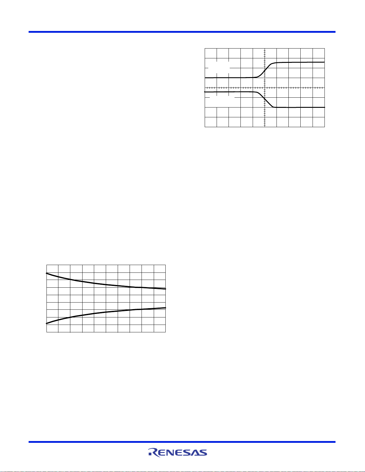
FIGURE 10. VOLTAGE MARGINING vs VMSET RESISTANCE
V
OUT
100m/DIV
V
OUT
100mV/DIV
2ms/DIV
FIGURE 11. VOLTAGE MARGINING SLEW TIME
A small ceramic capacitor should be placed in parallel with
R
to smooth the voltage across R
OCSET
OCSET
in the
presence of switching noise on the input voltage.
Voltage Margining
The ISL6420 has a voltage margining mode that can be
used for system testing. The voltage margining percentage
is resistor selectable up to ±10%. The voltage margining
mode can be enabled by connecting a margining set resistor
from VMSET/MODE pin to ground and using the control pins
GPIO1/REFIN and GPIO2 to toggle between positive and
negative margining (Refer to Table 2). With voltage
margining enabled, the VMSET resistor to ground sets a
current, which is switched to the FB pin. The current will be
equal to 2.468V divided by the value of the external resistor
tied to the VMSET/MODE pin.
The power supply output increases when GPIO2 is HIGH
and decreases when GPIO1/REFIN is HIGH. The amount
that the output voltage of the power supply changes with
voltage margining, will be equal to 2.468V times the ratio of
the external feedback resistor and the external resistor tied
to VMSET/MODE pin. Figure 9 shows the positive and
negative margining for a 3.3V output, using a 20.5k
feedback resistor and using various VMSET resistor values.
The slew time of the current is set by an external capacitor
on the CDEL pin, which is charged and discharged with a
100A current source. The change in voltage on the
capacitor is 2.5V. This same capacitor is used to set the
PGOOD active delay after soft-start. When PGOOD is low,
the internal PGOOD circuitry uses the capacitor and when
PGOOD is high the voltage margining circuit uses the
capacitor. The slew time for voltage margining can be in the
range of 300µs to 2ms.
External Reference/DDR Supply
The voltage margining can be disabled by connecting the
VMSET/MODE to VCC5. In this mode the chip can be
configured to work with an external reference input and
provide a buffered reference output.
FN9151 Rev 5.00 Page 13 of 20
Feb 13, 2008
If VMSET/MODE pin and the GPIO1/REFIN pin are both tied
to VCC5, then the internal 0.6V reference is used as the
error amplifier non-inverting input. The buffered reference
output on REFOUT will be 0.6V ±0.01V, capable of sourcing
20mA and sinking up to 50µA current with a 2.2µF capacitor
connected to the REFOUT pin.
If VMSET/MODE pin is tied to high but GPIO1/REFIN is
connected to external voltage source between 0.6V to 1.25V,
then this external voltage is used as the reference voltage at
the positive input of the error amplifier. The buffered
reference output on REFOUT will be Vrefin ±0.01V, capable
of sourcing 20mA and sinking up to 50µA current with a
2.2µF capacitor on the REFOUT pin.
Power Good
The PGOOD pin can be used to monitor the status of the
output voltage. PGOOD will be true (open drain) when the
FB pin is within ±10% of the reference and the ENSS pin has
completed its soft-start ramp.
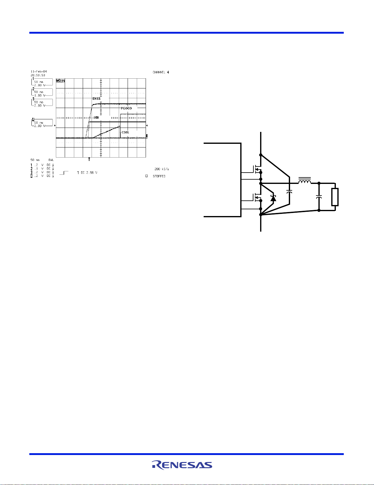
Additionally, a capacitor on the CDEL pin will set a delay for
the PGOOD signal. After the ENSS pin completes its softstart ramp, a 2µA current begins charging the CDEL
Page 14
ISL6420
FIGURE 12. PGOOD DELAY
GND
L
O
C
O
LGATE
UGATE
PHASE
Q1
Q2
D2
FIGURE 13. PRINTED CIRCUIT BOARD POWER AND
GROUND PLANES OR ISLANDS
V
IN
V
OUT
RETURN
ISL6420
C
IN
LOAD
capacitor to 2.5V. The capacitor will be quickly discharged
before PGOOD goes high. The programmable delay can be
used to sequence multiple converters or as a LOW-true
reset signal.
If the voltage on the FB pin exceeds ±10% of the reference,
then PGOOD will go low after 3µs of noise filtering.
Application Guidelines
Layout Considerations
As in any high frequency switching converter, layout is very
important. Switching current from one power device to
another can generate voltage transients across the
impedances of the interconnecting bond wires and circuit
traces. These interconnecting impedances should be
minimized by using wide, short printed circuit traces. The
critical components should be located as close together as
possible using ground plane construction or single point
grounding.
Over-Temperature Protection
The IC is protected against over temperature conditions.
When the junction temperature exceeds +150°C, the PWM
shuts off. Normal operation is resumed when the junction
temperature is cooled down to +130°C.
Shutdown
When ENSS pin is below 1V, the regulator is disabled with
the PWM output drivers tri-stated. When disabled, the IC
power will be reduced.
Under-Voltage
If the voltage on the FB pin is less than 15% of the reference
voltage for 8 consecutive PWM cycles, then the circuit enters
into soft-start hiccup mode. This mode is identical to the
overcurrent hiccup mode.
Overvoltage Protection
If the voltage on the FB pin exceeds the reference voltage by
15%, the lower gate driver is turned on continuously to
discharge the output voltage. If the overvoltage condition
continues for 32 consecutive PWM cycles, then the chip is
turned off with the gate drivers tri-stated. The voltage on the
FB pin will fall and reach the 15% undervoltage threshold.
After 8 clock cycles, the chip will enter soft-start hiccup
mode. This mode is identical to the overcurrent hiccup
mode.
FN9151 Rev 5.00 Page 14 of 20
Feb 13, 2008
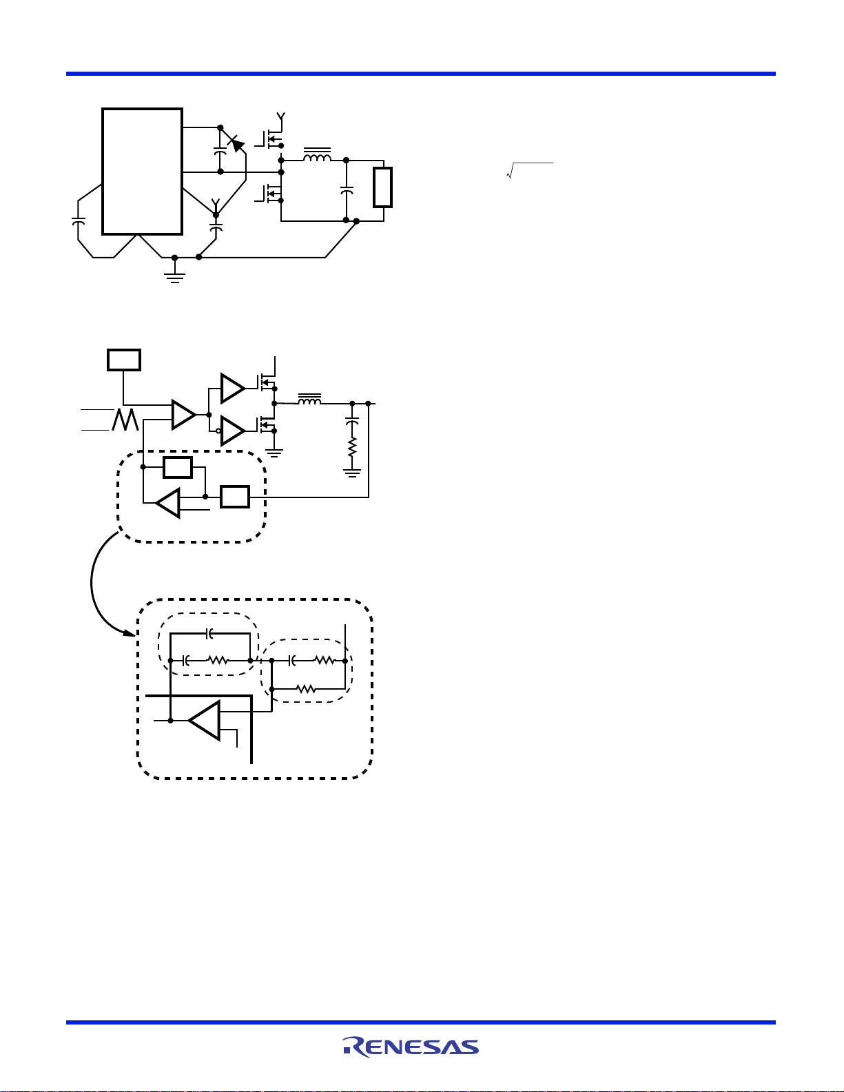
Figure 12 shows the critical power components of the
converter. To minimize the voltage overshoot the
interconnecting wires indicated by heavy lines should be part
of ground or power plane in a printed circuit board. The
components shown in Figure 12 should be located as close
together as possible. Please note that the capacitors C
and C
each represent numerous physical capacitors.
O
IN
Locate the ISL6420 within 3 inches of the MOSFETs, Q1 and
Q2. The circuit traces for the MOSFETs’ gate and source
connections from the ISL6420 must be sized to handle up to
1A peak current.
Figure 13 shows the circuit traces that require additional
layout consideration. Use single point and ground plane
construction for the circuits shown. Minimize any leakage
current paths on the ENSS PIN and locate the capacitor, C
ss
close to the ENSS pin because the internal current source is
only 30µA. Provide local V
GND pins. Locate the capacitor, C
decoupling between VCC and
CC
as close as practical
BOOT
to the BOOT and PHASE pins.
Feedback Compensation
Figure 14 highlights the voltage-mode control loop for a
synchronous-rectified buck converter. The output voltage
(Vout) is regulated to the Reference voltage level. The error
amplifier (Error Amp) output (V
) is compared with the
E/A
Page 15
ISL6420
FIGURE 14. PRINTED CIRCUIT BOARD SMALL SIGNAL
LAYOUT GUIDELINES
+5V
ISL6420
ENSS
GND
VCC
BOOT
D1
L
O
C
O
V
OUT
LOAD
Q1
Q2
PHASE
+V
IN
C
BOOT
C
VCC
C
SS
FIGURE 15. VOLTAGE - MODE BUCK CONVERTER
COMPENSATION DESIGN
V
OUT
OSC
REFERENCE
L
O
C
O
ESR
V
IN
V
OSC
ERROR
AMP
PWM
DRIVER
(PARASITIC)
-
REF
R1
R3
R2
C3
C2
C1
COMP
V
OUT
FB
Z
FB
ISL6420
Z
IN
COMPARATOR
DRIVER
DETAILED COMPENSATION COMPONENTS
PHASE
V
E/A
+
-
+
-
Z
IN
Z
FB
+
F
LC
1
2 L
OCO
---------------------------------------=
(EQ. 4)
F
ESR
1
2 ESR C
O
---------------------------------------------=
(EQ. 5)
F
Z1
1
2 R 2C1
----------------------------------=
(EQ. 6)
F
P1
1
2 R2
C1 C2
C1 C2+
----------------------
-------------------------------------------------------=
(EQ. 7)
F
Z2
1
2 R1 R3+C3
------------------------------------------------------=
(EQ. 8)
FP2 =
1
2 R3 C3
----------------------------------
(EQ. 9)
the modulator is simply the input voltage (VIN) divided by the
peak-to-peak oscillator voltage V
OSC
.
Modulator Break Frequency Equations
The compensation network consists of the error amplifier
(internal to the ISL6420) and the impedance networks Z
and Z
. The goal of the compensation network is to provide
FB
IN
a closed loop transfer function with the highest 0dB crossing
frequency (f
is the difference between the closed loop phase at f
o
180
. The equations below relate the compensation
) and adequate phase margin. Phase margin
0dB
0dB
and
network’s poles, zeros and gain to the components (R1, R2,
R3, C1, C2, and C3) in Figure 14. Use these guidelines for
locating the poles and zeros of the compensation network:
Compensation Break Frequency Equations
oscillator (OSC) triangular wave to provide a pulse-width
modulated (PWM) wave with an amplitude of V
PHASE node. The PWM wave is smoothed by the output filter
(L
and CO).
O
The modulator transfer function is the small-signal transfer
function of Vout/V
Gain and the output filter (L
break frequency at F
E/A
. This function is dominated by a DC
and a zero at F
LC
and CO), with a double pole
O
. The DC Gain of
ESR
at the
IN
1. Pick Gain (R2/R1) for desired converter bandwidth
ST
2. Place 1
Zero Below Filter’s Double Pole
(~75% FLC)
ND
3. Place 2
4. Place 1
5. Place 2
Zero at Filter’s Double Pole
ST
Pole at the ESR Zero
ND
Pole at Half the Switching Frequency
6. Check Gain against Error Amplifier’s Open-Loop Gain
7. Estimate Phase Margin - Repeat if Necessary
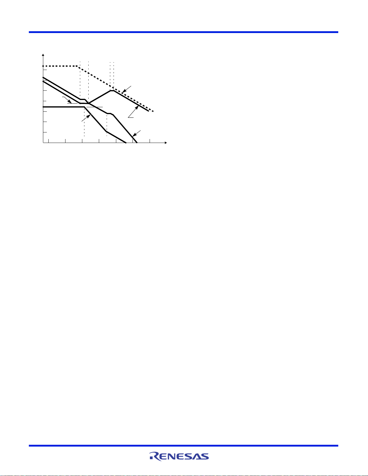
Figure 15 shows an asymptotic plot of the DC/DC
converter’s gain vs. frequency. The actual Modulator Gain
has a high gain peak do to the high Q factor of the output
filter and is not shown in Figure 15. Using the above
guidelines should give a Compensation Gain similar to the
curve plotted. The open loop error amplifier gain bounds the
compensation gain. Check the compensation gain at F
P2
with the capabilities of the error amplifier. The Loop Gain is
constructed on the log-log graph of Figure 15 by adding the
Modulator Gain (in dB) to the Compensation Gain (in dB).
This is equivalent to multiplying the modulator transfer
FN9151 Rev 5.00 Page 15 of 20
Feb 13, 2008
Page 16
ISL6420
100
80
60
40
20
0
-20
-40
-60
F
P1
F
Z2
10M1M100k10k1k10010
OPEN LOOP
ERROR AMP GAIN
F
Z1
F
P2
F
LC
F
ESR
COMPENSATION
GAIN (dB)
FREQUENCY (Hz)
GAIN
20LOG
(V
IN
/V
OSC
)
MODULATOR
GAIN
20LOG
(R2/R1)
LOOP GAIN
FIGURE 16. ASYMPTOTIC BODE PLOT OF CONVERTER GAIN
I
L
VIN - V
OUT
Fs x L
--------------------------------
V
OUT
V
IN
----------------
=
(EQ. 10)
V
OUT
IL ESR=
(EQ. 11)
function to the compensation transfer function and plotting
the gain.
The compensation gain uses external impedance networks
Z
and ZIN to provide a stable, high bandwidth (BW) overall
FB
loop. A stable control loop has a gain crossing with 20dB/decade slope and a phase margin greater than 45°.
Include worst case component variations when determining
phase margin.
Use only specialized low-ESR capacitors intended for
switching-regulator applications for the bulk capacitors.
The bulk capacitor’s ESR will determine the output ripple
voltage and the initial voltage drop after a high slew-rate
transient. An aluminum electrolytic capacitor's ESR value is
related to the case size with lower ESR available in larger
case sizes. However, the equivalent series inductance (ESL)
of these capacitors increases with case size and can reduce
the usefulness of the capacitor to high slew-rate transient
loading. Unfortunately, ESL is not a specified parameter.
Work with your capacitor supplier and measure the
capacitor’s impedance with frequency to select a suitable
component. In most cases, multiple electrolytic capacitors of
small case size perform better than a single large case
capacitor.
Output Inductor Selection
The output inductor is selected to meet the output voltage
ripple requirements and minimize the converter’s response
time to the load transients. The inductor value determines
the converter’s ripple current and the ripple voltage is a
function of the ripple current and the output capacitors ESR.
The ripple voltage and current are approximated by the
following equations:
Component Selection Guidelines
Output Capacitor Selection
An output capacitor is required to filter the output and supply
the load transient current. The filtering requirements are a
function of the switching frequency and the ripple current.
The load transient requirements are a function of the slew
rate (di/dt) and the magnitude of the transient load current.
These requirements are generally met with a mix of
capacitors and careful layout.
Modern microprocessors produce transient load rates above
1A/ns. High frequency capacitors initially supply the transient
and slow the current load rate seen by the bulk capacitors.
The bulk filter capacitor values are generally determined by
the ESR (effective series resistance) and voltage rating
requirements rather than actual capacitance requirements.
High frequency decoupling capacitors should be placed as
close to the power pins of the load as physically possible. Be
careful not to add inductance in the circuit board wiring that
could cancel the usefulness of these low inductance
components. Consult with the manufacturer of the load on
specific decoupling requirements. For example, Intel
recommends that the high frequency decoupling for the
Pentium Pro be composed of at least forty (40) 1.0µF
ceramic capacitors in the 1206 surface-mount package.
FN9151 Rev 5.00 Page 16 of 20
Feb 13, 2008
Increasing the value of inductance reduces the ripple current
and voltage. However, larger inductance values reduce the
converter’s response time to a load transient.
One of the parameters limiting the converter’s response to a
load transient is the time required to change the inductor
current. Given a sufficiently fast control loop design, the
ISL6420 will provide either 0% or 100% duty cycle in
response to a load transient. The response time is the time
required to slew the inductor current from an initial current
value to the transient current level. During this interval the
difference between the inductor current and the transient
current level must be supplied by the output capacitor.
Minimizing the response time can minimize the output
capacitance required.
Page 17

ISL6420
t
RISE
LOI
TRAN
V
INVOUT
–
--------------------------------=
(EQ. 12)
t
FALL
LOI
TRAN
V
OUT
-------------------------------=
(EQ. 13)
I
RMSIMAX
DD2–=
(EQ. 14)
P
UFETIO
2
R
DS ON
D
1
2
---
I
OVINtswfsw
+=
(EQ. 15)
P
LFETIO
2
R
DS ON
1D–=
(EQ. 16)
The response time to a transient is different for the application
of load and the removal of load. The following equations give
the approximate response time interval for application and
removal of a transient load:
where: I
response time to the application of load, and t
is the transient load current step, t
TRAN
FALL
RISE
is the
is the
response time to the removal of load. With a +5V input source,
the worst case response time can be either at the application
or removal of load and dependent upon the output voltage
setting. Be sure to check both of these equations at the
minimum and maximum output levels for the worst case
response time.
Input Capacitor Selection
Use a mix of input bypass capacitors to control the voltage
overshoot across the MOSFETs. Use small ceramic capacitors
for high frequency decoupling and bulk capacitors to supply the
current needed each time Q1 turns on. Place the small ceramic
capacitors physically close to the MOSFETs and between the
drain of Q1 and the source of Q2.
The important parameters for the bulk input capacitor are the
voltage rating and the RMS current rating. For reliable
operation, select the bulk capacitor with voltage and current
ratings above the maximum input voltage and largest RMS
current required by the circuit. The capacitor voltage rating
should be at least 1.25 times greater than the maximum input
voltage and a voltage rating of 1.5 times is a conservative
guideline. The RMS current rating requirement for the input
capacitor of a buck regulator is approximately 1/2 the DC load
current. A more specific equation for determining the input
ripple is the following,
For a through hole design, several electrolytic capacitors
(Panasonic HFQ series or Nichicon PL series or Sanyo MV-GX
or equivalent) may be needed. For surface mount designs,
solid tantalum capacitors can be used, but caution must be
exercised with regard to the capacitor surge current rating.
These capacitors must be capable of handling the surgecurrent at power-up. The TPS series available from AVX, and
the 593D series from Sprague are both surge current tested.
MOSFET Selection/Considerations
The ISL6420 requires 2 N-Channel power MOSFETs. These
should be selected based upon r
DS(ON)
, gate supply
requirements, and thermal management requirements.
In high-current applications, the MOSFET power dissipation,
package selection and heatsink are the dominant design
factors. The power dissipation includes two loss components;
conduction loss and switching loss.
The conduction losses are the largest component of power
dissipation for both the upper and the lower MOSFETs. These
losses are distributed between the two MOSFETs according to
duty factor (see the equations below). Only the upper
MOSFET has switching losses, since the Schottky rectifier
clamps the switching node before the synchronous rectifier
turns on.
Where D is the duty cycle = Vo/Vin, tsw is the switching
interval, and Fsw is the switching frequency.
These equations assume linear voltage-current transitions and
do not adequately model power loss due the reverse-recovery
of the lower MOSFETs body diode. The gate-charge losses are
dissipated by the ISL6420 and don't heat the MOSFETs.
However, large gate-charge increases the switching interval,
t
which increases the upper MOSFET switching losses.
SW
Ensure that both MOSFETs are within their maximum junction
temperature at high ambient temperature by calculating the
temperature rise according to package thermal-resistance
specifications. A separate heatsink may be necessary
depending upon MOSFET power, package type, ambient
temperature and air flow.
Schottky Selection
Rectifier D2 is a clamp that catches the negative inductor swing
during the dead time between turning off the lower MOSFET
and turning on the upper MOSFET. The diode must be a
Schottky type to prevent the parasitic MOSFET body diode from
conducting. It is acceptable to omit the diode and let the body
diode of the lower MOSFET clamp the negative inductor swing,
but efficiency will drop one or two percent as a result. The
diode's rated reverse breakdown voltage must be greater than
the maximum input voltage.
FN9151 Rev 5.00 Page 17 of 20
Feb 13, 2008
Page 18

ISL6420
© Copyright Intersil Americas LLC 2004-2008. All Rights Reserved.
All trademarks and registered trademarks are the property of their respective owners.
For additional products, see www.intersil.com/en/products.html
Intersil products are manufactured, assembled and tested utilizing ISO9001 quality systems as noted
in the quality certifications found at www.intersil.com/en/support/qualandreliability.html
Intersil products are sold by description only. Intersil may modify the circuit design and/or specifications of products at any time without notice, provided that such
modification does not, in Intersil's sole judgment, affect the form, fit or function of the product. Accordingly, the reader is cautioned to verify that datasheets are
current before placing orders. Information furnished by Intersil is believed to be accurate and reliable. However, no responsibility is assumed by Intersil or its
subsidiaries for its use; nor for any infringements of patents or other rights of third parties which may result from its use. No license is granted by implication or
otherwise under any patent or patent rights of Intersil or its subsidiaries.
For information regarding Intersil Corporation and its products, see www.intersil.com
FN9151 Rev 5.00 Page 18 of 20
Feb 13, 2008
Page 19
ISL6420
located within the zone indicated. The pin #1 identifier may be
Unless otherwise specified, tolerance : Decimal ± 0.05
Tiebar shown (if present) is a non-functional feature.
The configuration of the pin #1 identifier is optional, but must be
between 0.15mm and 0.30mm from the terminal tip.
Dimension b applies to the metallized terminal and is measured
Dimensions in ( ) for Reference Only.
Dimensioning and tolerancing conform to AMSE Y14.5m-1994.
6.
either a mold or mark feature.
3.
5.
4.
2.
Dimensions are in millimeters.1.
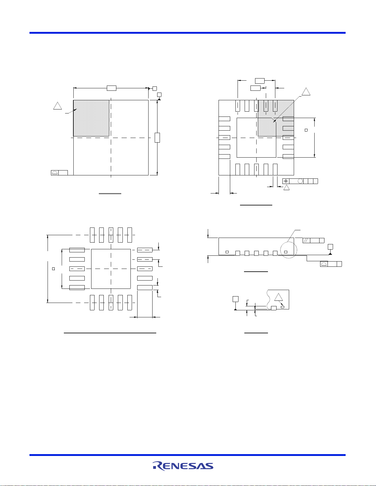
NOTES:
BOTTOM VIEW
DETAIL "X"
TYPICAL RECOMMENDED LAND PATTERN
TOP VIEW
BOTTOM VIEW
SIDE VIEW
4.00
A
4.00
B
6
PIN 1
INDEX AREA
(4X)
0.15
4X
0.50
2.0
16X
2016
15
11
PIN #1 INDEX AREA
6
2 . 10 ± 0 . 15
5
1
0.25 +0.05 / -0.07
0.10 M ABC
20X 0.6 +0.15 / -0.25
4
6
10
BASE PLANE
SEATING PLANE
0.10
SEE DETAIL "X"
0.08 C
C
C
0 . 90 ± 0 . 1
0 . 2 REF
C
0 . 05 MAX.
0 . 00 MIN.
5
( 3. 6 TYP )
( 2. 10 )
( 20X 0 . 8)
( 20X 0 . 5 )
( 20X 0 . 25 )
Package Outline Drawing
L20.4x4
20 LEAD QUAD FLAT NO-LEAD PLASTIC PACKAGE
Rev 1, 11/06
FN9151 Rev 5.00 Page 19 of 20
Feb 13, 2008
Page 20
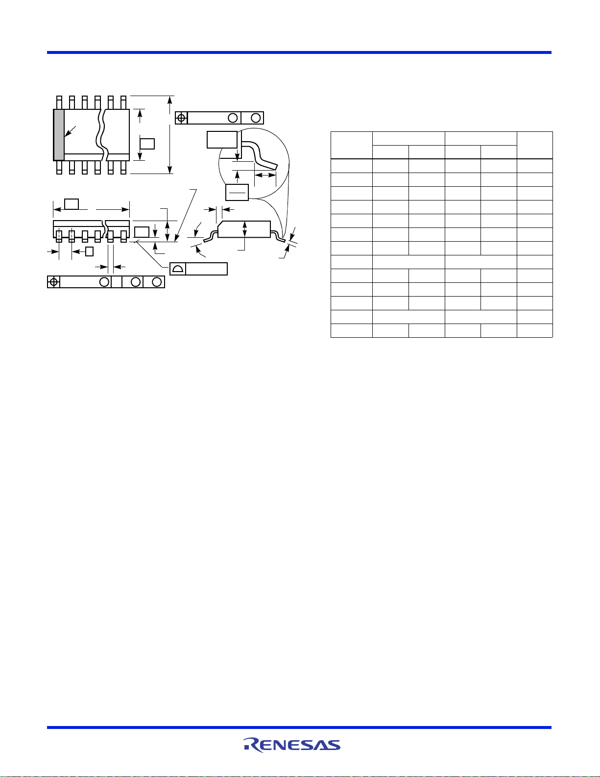
ISL6420
NOTES:
1. Symbols are defined in the “MO Series Symbol List” in Section 2.2 of
Publication Number 95.
2. Dimensioning and tolerancing per ANSI Y14.5M-1982.
3. Dimension “D” does not include mold flash, protrusions or gate burrs.
Mold flash, protrusion and gate burrs shall not exceed 0.15mm
(0.006 inch) per side.
4. Dimension “E” does not include interlead flash or protrusions. Interlead flash and protrusions shall not exceed 0.25mm (0.010 inch) per
side.
5. The chamfer on the body is optional. If it is not present, a visual index
feature must be located within the crosshatched area.
6. “L” is the length of terminal for soldering to a substrate.
7. “N” is the number of terminal positions.
8. Terminal numbers are shown for reference only.
9. Dimension “B” does not include dambar protrusion. Allowable dambar protrusion shall be 0.10mm (0.004 inch) total in excess of “B” dimension at maximum material condition.
10. Controlling dimension: INCHES. Converted millimeter dimensions
are not necessarily exact.
INDEX
AREA
E
D
N
123
-B-
0.17(0.007) C AM BS
e
-A-
B
M
-C-
A1
A
SEATING PLANE
0.10(0.004)
h x 45°
C
H
0.25(0.010) BM M
L
0.25
0.010
GAUGE
PLANE
A2
Shrink Small Outline Plastic Packages (SSOP)
Quarter Size Outline Plastic Packages (QSOP)
M20.15
20 LEAD SHRINK SMALL OUTLINE PLASTIC PACKAGE
(0.150” WIDE BODY)
INCHES MILLIMETERS
SYMBOL
A 0.053 0.069 1.35 1.75 -
A1 0.004 0.010 0.10 0.25 -
A2 - 0.061 - 1.54 -
B 0.008 0.012 0.20 0.30 9
C 0.007 0.010 0.18 0.25 -
D 0.337 0.344 8.56 8.74 3
E 0.150 0.157 3.81 3.98 4
e 0.025 BSC 0.635 BSC -
H 0.228 0.244 5.80 6.19 -
h 0.0099 0.0196 0.26 0.49 5
L 0.016 0.050 0.41 1.27 6
N20 207
0° 8° 0° 8° -
NOTESMIN MAX MIN MAX
Rev. 1 6/04
FN9151 Rev 5.00 Page 20 of 20
Feb 13, 2008
 Loading...