

Page 1
®
www.BDTIC.com/Intersil
ISL6405
Data Sheet July 2004
Dual Output LNB Supply and Control
Voltage Regulator with I2C Interface for
Advanced Satellite Set-Top Box Designs
The ISL6405 is a highly integrated voltage regulator and
interface IC, specifically designed for supplying power and
control signals from advanced satellite set-top box (STB)
modules to the low noise blocks (LNBs) of two antenna
ports. The device is comprised of two independent currentmode boost PWMs and two low-noise linear regulators along
with the circuitry required for 22kHz tone generation,
modulation and I
total LNB supply design simple, efficient and compact with
low external component count.
Two independent current-mode boost converters provide the
linear regulators with input voltages that are set to the final
output voltages, plus typically 1.2V to insure minimum power
dissipation across each linear regulator. This maintains
constant voltage drops across each linear pass element
while permitting adequate voltage range for tone injection.
The final regulated output voltages are available at two
output terminals to support simultaneous operation of two
antenna ports for dual tuners. The outputs for each PWM are
set to 13V or 18V by independent voltage select commands
(VSEL1, VSEL2) through the I
compensate for the voltage drop in the coaxial cable, the
selected voltage may be increased by 1V with the line length
compensation (LLC) feature. All the functions on this IC are
controlled via the I
Register (SR, 8 bits). The same register can be read back,
and two bits will report the diagnostic status. Separate enable
commands sent on the I
mode control for each PWM and linear combination, disabling
the output into shutdown mode.
Each output channel is capable of providing 750mA of
continuous current. The overcurrent limit can be digitally
programmed. The SEL18V pin with QFN package allows the
13V to 18V transition with an external pin, over-riding the I
input.
2
C device interface. The device makes the
2
C bus. Additionally, to
2
C bus by writing 8 bits on System
2
C bus provide independent standby
2
C
FN9026.2
Features
• Single Chip Power solution
- True Dual Operation for 2-Tuner/2-Dish Applications
- Both Outputs May be Enabled Simultaneously at
Maximum Power
- Integrated DC-DC Converter and I
• Switch-Mode Power Converter for Lowest Dissipation
- Boost PWMs with > 92% Efficiency
- Selectable 13V or 18V Outputs
- Digital Cable Length Compensation (1V)
2
•I
C Compatible Interface for Remote Device Control
- Registered Slave Address 0001 00XX
- Full 3.3V/5V Operation up to 400kHz
• External Pins to Select 13V/18V Options
- Available with QFN Package Only
• Built-In Tone Oscillator Factory Trimmed to 22kHz
- Facilitates DiSEqC
• Internal Over-Temperature Protection and Diagnostics
• Internal Overload and Overtemp Flags (Visible on I
• LNB Short-Circuit Protection and Diagnostics
• QFN Package
- Compliant to JEDEC PUB95 MO-220 QFN - Quad Flat
No Leads - Product Outline
- Near Chip-Scale Package Footprint
• Pb-free Packaging Available
- Designated with “Z” Suffix (Refer to Note Below)
(EUTELSAT) Encoding
TM
2
C Interface
2
C)
Applications
• LNB Power Supply and Control for Satellite Set-Top Box
References
• Tech Brief 389 (TB389) - “PCB Land Pattern Design and
Surface Mount Guidelines for QFN Packages”; Available
on the Intersil website, www.intersil.com
Ordering Information
PART # TEMP. RANGE (oC) PACKAGE PKG. DWG. #
ISL6405EEB -20 to 85 28 Ld EPSOIC M28.3B
ISL6405EEBZ
(Note 1)
ISL6405ER -20 to 85 32 Ld 5x5 QFN L32.5x5
ISL6405ERZ
(Note 1)
NOTES:
1. Intersil Pb-free products employ special Pb-free material sets; mo lding
compounds/die attach materials and 100% matte tin plate termination
finish, which is compatible with both SnPb and Pb-free soldering
operations. Intersil Pb-free products are MSL classified at Pb-free peak
reflow temperatures that meet or exceed the Pb-free requirements of
IPC/JEDEC J Std-020B.
2. Tape and Reel available. Add “-T” suffix for Tape and Reel Packing Option.
-20 to 85 28 Ld EPSOIC
(Pb-free)
-20 to 85 32 Ld 5x5 QFN
(Pb-free)
M28.3B
L32.5x5
1
CAUTION: These devices are sensitive to electrostatic discharge; follow proper IC Handling Procedures.
1-888-INTERSIL or 321-724-7143
| Intersil (and design) is a trademark of Intersil Americas Inc.
Copyright © Intersil Americas Inc. 2004. All Rights Reserved
Page 2
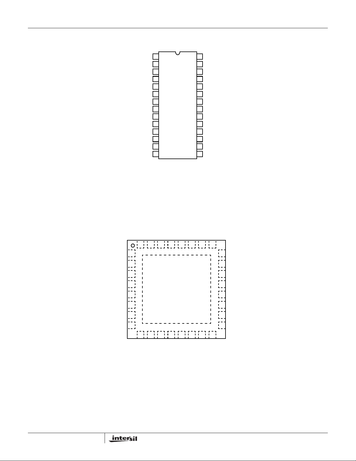
VSW2
www.BDTIC.com/Intersil
COMP2
FB2
GATE2
PGND 2
CS2
SGND
BYPASS
PGND1
GATE1
CS1
FB1
COMP1
VSW1
ISL6405
ISL6405 (EPSOIC)
TOP VIEW
1
2
3
4
5
6
ISL6405EEB
7
8
9
10
11
12
13
14
28
VCC
CPVOUT
27
CPSWIN
26
CPSWOUT
25
TCAP2
24
DSQIN2
23
VO2
22
AGND
21
20
VO1
DSQIN1
19
TCAP1
18
SCL
17
16
ADDR
SDA
15
PGND2
CS2
SGND
SEL18V1
SEL18V2
BYP
PGND1
GATE1
ISL6405 (QFN)
TOP VIEW
VCC
NC
FB2
GATE2
32 31 30 29 28 27 26 25
1
2
3
4
5
6
7
8
9 10111213141516
FB1
CS1
VSW2
COMP2
ISL6405ER
VSW1
COMP1
NC
SDA
CPVOUT
ADDR
SCL CPSWIN
24
23
22
21
20
19
18
17
CPSWOUT
TCAP2
DSQIN2
VO2
AGND
VO1
DSQIN1
TCAP1
2
Page 3
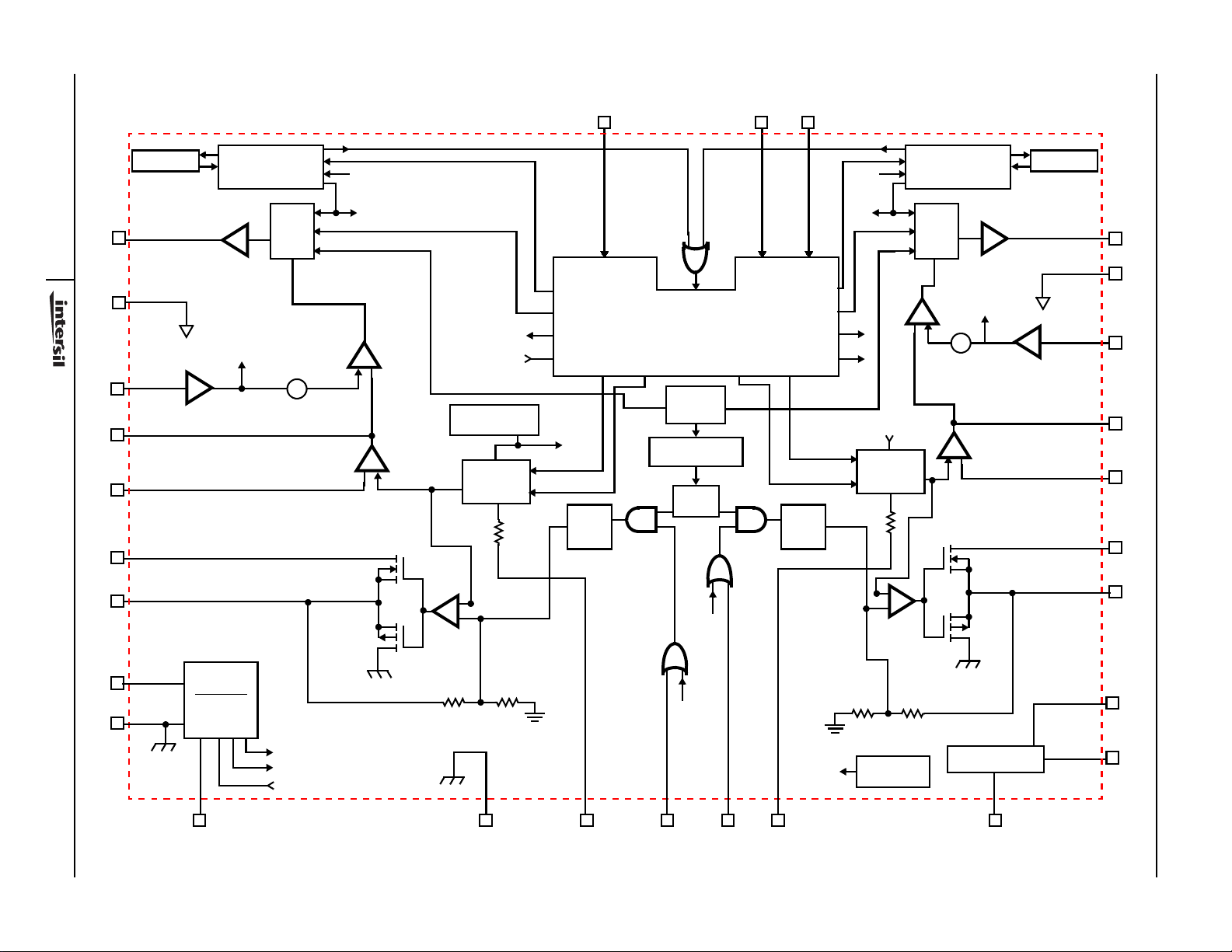
Block Diagram
www.BDTIC.com/Intersil
15 16 17
CLK1
SLOPE
OLF1
DCL
OC1
+
-
+
VREF1
BAND GAP
REF VOLTAGE
REF
VO LTAG E
ADJ1
+
-
SDA
SDA
ISEL1
EN1
ENT1
OTF
LLC1 VSEL1 VSEL2 LLC2
CLK1
BGV
TONE
INJ
CKT 1
OLF
I2C
INTERFACE
OSC.
220kHz
10 &
÷
WAVE SHAPING
22kHz
TONE
ENT2
CLK2
ADDR
SCLADDR
TONE
INJ
CKT 2
COUNTER
GATE1
10
3
PGND1
9
CS1
11
COMP1
13
FB1
12
VSW1
14
VO1
20
OVERCURRENT
PROTECTION
LOGIC SCHEME 1
ILIM1
CS
AMP
PWM
LOGIC
Q
S
∑
COMPENSATION
SCL
ISEL2
EN2
ENT2
DCL
OLF2
DCL
OC2
VOLTAGE
OVERCURRENT
LOGIC SCHEME 2
CLK2
BGV
REF
ADJ2
+
-
PROTECTION
PWM
LOGIC
Q
S
-
ILIM2
+
∑
SLOPE
COMPENSATION
+
-
VREF2
CS
AMP
COUNTER
GATE2
PGND2
CS2
COMP2
FB2
VSW2
VO2
4
5
6
2
ISL6405
3
1
22
VCC
28
SGND
7
ON CHIP
LINEAR
UVLO
POR
SOFT-START
BYPASS
8
INT 5V
SOFT-START
EN1/EN2
AGND
21
TCAP1
18 19
DSQIN1
ENT1
DSQIN2
23
OTF
TCAP2
24 25
THERMAL
SHUTDOWN
CHARGE PUMP
CPSWOUT
CPVOUT
CPSWIN
27
26
Page 4
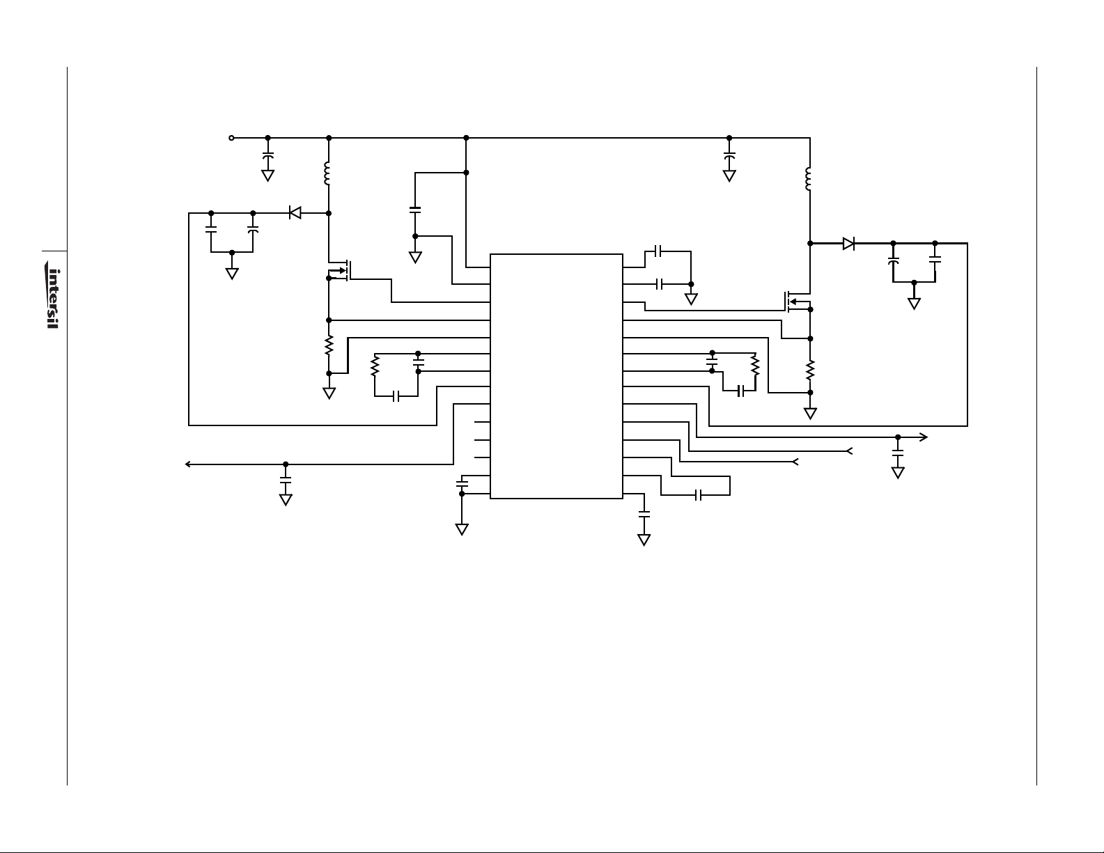
Typical Application Schematic
www.BDTIC.com/Intersil
VIN = 8V TO 14V
4
VO1
13V/18V
+
C3
L1
D1
+
C2C1
Q1
R1
C15
R2
C5
C4
C12
C16
28
7
10
11
9
13
12
14
20
19
23
16
18
21
VCC
SGND
GATE1
CS1
PGND1
COMP1
FB1
VSW1
VO1
DSQIN1
DSQIN2
ADDR
TCAP1
AGND
CPSWOUT
CPVOUT
ISL6405EEB
TCAP2
BYPASS
GATE2
CS2
PGND2
COMP2
FB2
VSW2
VO2
SCL
SDA
CPSWIN
C9
C20
24
C6
8
4
6
5
R3
2
3
1
22
17
15
26
25
27
C13
C8
+
C14
R3
C7
L2
SDA
R4
Q2
D2
SCL
+
C11C10
ISL6405
VO2
13V/18V
C17
Page 5
ISL6405
www.BDTIC.com/Intersil
Absolute Maximum Ratings Thermal Information
Supply Voltage, VCC . . . . . . . . . . . . . . . . . . . . . . . . . . 8.0V to 18.0V
Logic Input Voltage Range (SDA, SCL, ENT) . . . . . . . . -0.5V to 7V
CAUTION: Stresses above those listed in “Absolute Maximum Ratings” may cause permanent damage to the device. This is a stress only rating and operation of the
device at these or any other conditions above those indicated in the operational sections of this specification is not implied.
3. θJA is measured in free air with the component mounted on a high effective thermal conductivity test board with “direct attach” features. See
Tech Brief TB379.
4. For θ
5. The device junction temperature should be kept below 150
, the "case temp" location is the center of the exposed metal pad on the package underside.
+150
JC
o
C typically.
o
C. Thermal shut-down circuitry turns off the device if junction temperature exceeds
Thermal Resistance (Typical, Notes 3, 4) θJA (oC/W) θJC (oC/W)
EPSOIC Package (Notes 3, 4). . . . . . . 29 4
QFN Package (Notes 3, 4). . . . . . . . . . 34 6
Maximum Junction Temperature (Note 5) . . . . . . . . . . . . . . . .150
Maximum Storage Temperature Range . . . . . . . . . . -40
Maximum Lead Temperature (Soldering 10s) . . . . . . . . . . . . .300
(SOIC - Lead Tips Only)
Operating Temperature Range . . . . . . . . . . . . . . . . . -20
o
C to 150oC
o
C to 85oC
o
o
C
C
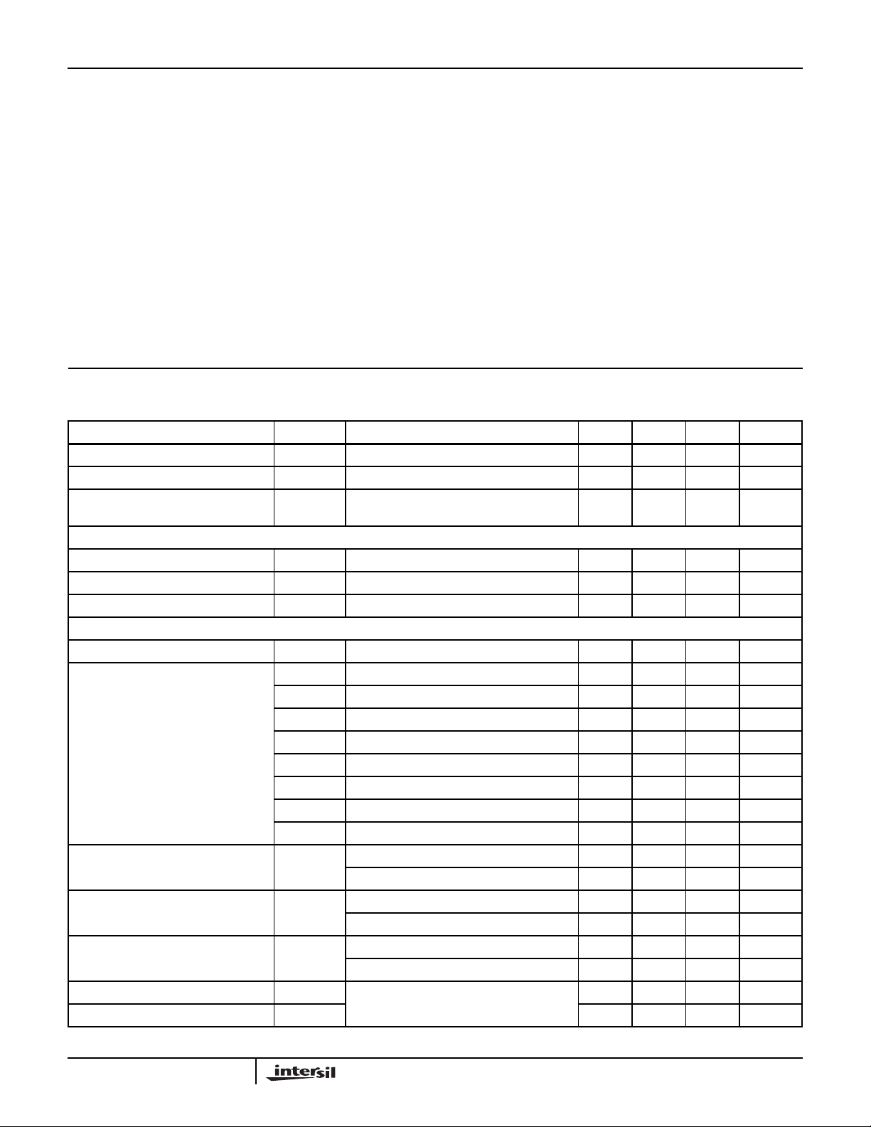
Electrical Specifications V
PARAMETER SYMBOL TEST CONDITIONS MIN TYP MAX UNITS
Operating Supply Voltage Range 81214 V
Standby Supply Current EN1 = EN2 = L - 1.5 3.0 mA
Supply Current I
UNDER VOLTAGE LOCKOUT
Start Threshold 7.5 - 7.95 V
Stop Threshold 7.0 - 7.55 V
Start to Stop Hysteresis 350 400 500 mV
SOFT START
COMP Rise Time (Note 6) (Note 7) - 512 - Cycles
Output Voltage (Note 7) V
Line Regulation DV
Load Regulation DV
Dynamic Output Current Limiting I
Dynamic Overload Protection Off Time TOFF DCL = L, Output Shorted (Note 8) - 900 - ms
Dynamic Overload Protection On Time TON - 20 - ms
= 12V, TA = -20oC to +85oC, unless otherwise noted. Typical values are at TA = 25oC. EN1 = EN2 = H,
CC
LLC1 = LLC2 = L, ENT1 = ENT2 = L, DCL = L, DSQIN1 = DSQIN2 = L, Iout = 12mA, unless otherwise noted.
See software description section for I
EN1 = EN2 = LLC1 = LLC2 = VSEL1 =
VSEL2 = ENT1 = ENT2 = H, No Load
VSEL1 = L, LLC1 = L 12.74 13.0 13.26 V
VSEL1 = L, LLC1 = H 13.72 14.0 14.28 V
VSEL1 = H, LLC1 = L 17.64 18.0 18.36 V
VSEL1 = H, LLC1 = H 18.62 19.0 19.38 V
VSEL2 = L, LLC2 = L 12.74 13.0 13.26 V
VSEL2 = L, LLC2 = H 13.72 14.0 14.28 V
VSEL2 = H, LLC2 = L 17.64 18.0 18.36 V
VSEL2 = H, LLC2 = H 18.62 19.0 19.38 V
VIN = 8V to 14V; VO1, VO2 = 13V - 4.0 40.0 mV
O1,
O2
O1,
O2
= 8V to 14V; VO1, VO2 = 18V - 4.0 60.0 mV
V
IN
IO = 12mA to 350mA - 50 80 mV
= 12mA to 750mA (Note 8) - 100 200 mV
I
O
DCL = L, ISEL1/2 = L 425 - 550 mA
DCL = L, ISEL1/2 = H (Note 8) 775 850 950 mA
V
V
V
V
V
V
V
DV
DV
IN
O1
O1
O1
O1
O2
O2
O2
O2
MAX
2
C access to the system.
-4.08.0mA
5
Page 6
ISL6405
www.BDTIC.com/Intersil
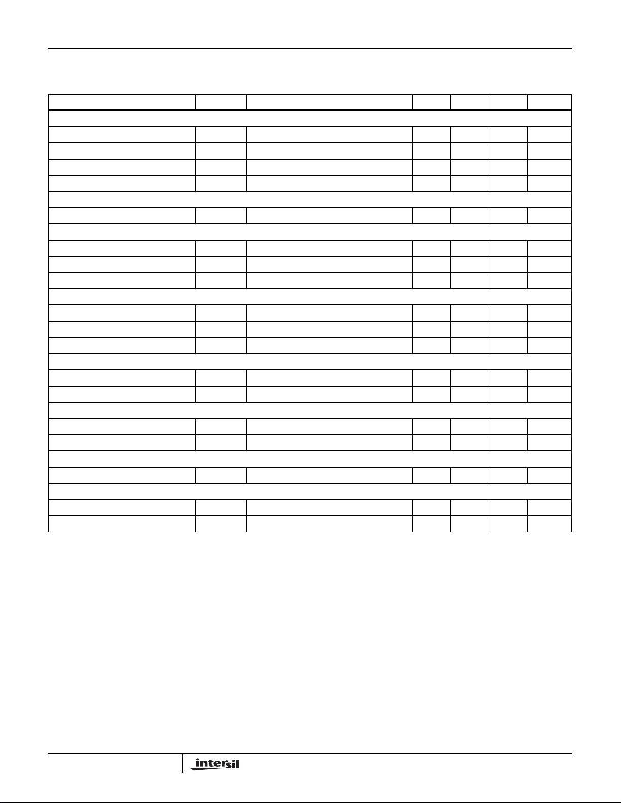
Electrical Specifications V
PARAMETER SYMBOL TEST CONDITIONS MIN TYP MAX UNITS
22kHz TONE SECTION
Tone Frequency f
Tone Amplitude V
Tone Duty Cycle dc
Tone Rise or Fall Time Tr, T
LINEAR REGULATOR
Drop-out Voltage Iout = 750mA (Note 8) - 1.2 - V
DSQIN PIN
DSQIN pin logic Low - - 1.5V V
DSQIN pin Logic HIGH 3.0 - - V
DSQIN pin Input Current -1-µA
CURRENT SENSE
Pulse by Pulse Current Limit (max Vin) 150 200 250 mV
Input Bias Current I
Over Current Threshold Static current mode, DCL = H 325 400 500 mV
ERROR AMPLIFIER
Open Loop Voltage Gain A
Gain Bandwidth Product
PWM
Maximum Duty Cycle 90 93 - %
Minimum Pulse Width (Note 8) - 20 - ns
OSCILLATOR
Oscillator Frequency f
Thermal Shutdown
Temperature Shutdown Threshold (Note 8) - 150 -
Temperature Shutdown Hysteresis (Note 8) - 20 -
NOTES:
6. Internal Digital Soft-start
7. VO1 for LNB1, VO2 for LNB2. Voltage programming signals VSEL1, VSEL2, LLC1, and LLC2 are implemented via the I
IO1 = IO2 = 350mA/750mA.
8. Guaranteed by Design
= 12V, TA = -20oC to +85oC, unless otherwise noted. Typical values are at TA = 25oC. EN1 = EN2 = H,
CC
LLC1 = LLC2 = L, ENT1 = ENT2 = L, DCL = L, DSQIN1 = DSQIN2 = L, Iout = 12mA, unless otherwise noted.
See software description section for I
tone
tone
tone
BIAS
OL
GBP
ENT1/2 = H 20.0 22.0 24.0 kHz
ENT1/2 = H 500 680 800 mV
ENT1/2 = H 405060 %
ENT1/2 = H 5 8 14 µs
f
(Note 8) 70 88 - dB
(Note 8) 10 - - MHz
Fixed at (10)(f
o
2
C access to the system. (Continued)
- 700 - nA
) 200 220 240 kHz
tone
2
C bus.
6
Page 7
ISL6405
www.BDTIC.com/Intersil
Functional Pin Description
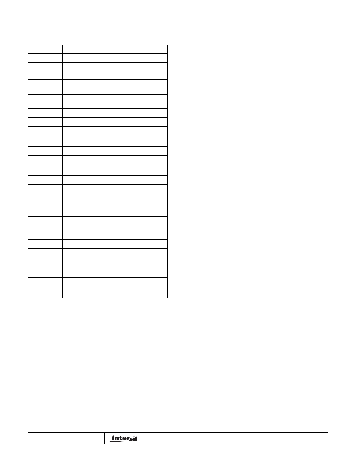
SYMBOL FUNCTION
2
SDA Bidirectional data from/to I
2
SCL Clock from I
VSW1, 2 Input of the linear post-regulator.
PGND1, 2 Dedicated ground for the output gate driver of
respective PWM.
CS1, 2 Current sense input; connect Rsc at this pin for
SGND Small signal ground for the IC.
AGND Analog ground for the IC.
TCAP1, 2 Capacitor for setting rise and fall time of the output
BYPASS Bypass capacitor for internal 5V.
DSQIN1, 2 When HIGH enables internal 22kHz modulation for
VCC Main power supply to the chip.
GATE1, 2 These are the device outputs of PWM A and
VO1, 2 Output voltage of LNB A and LNB B respectively.
ADDR Address pin to select two different addresses per
COMP1, 2 Error amp outputs used for compensation.
FB1, 2 Feedback pins for respective PWMs
CPVOUT,
CPSWIN,
CPSWOUT
SEL18V1, 2 When connected HIGH, this pin will change the
desired over current value for respective PWM.
of LNB A and LNB B respectively. Use this
capacitor value 1µF or higher.
LNB A and LNA B respectively, Use this pin for
tone enable function for LNB A and LNB B.
PWM B respectively. These high current driver
outputs are capable of driving the gate of a power
FET. These outputs are actively held low when
Vcc is below the UVLO threshold.
voltage level at this pin.
Charge pump connections.
output of the respective PWM to 18V. Only
available on the QFN package option.
C bus.
C bus.
Functional Description
The ISL6405 dual output voltage regulator makes an ideal
choice for advanced satellite set-top box and personal video
recorder applications. Both supply and control voltage
outputs for two low-noise blocks (LNBs) are available
simultaneously in any output configuration. The device
utilizes built-in DC/DC step-converters that, from a single
supply source ranging from 8V to 14V, generate the voltages
that enable the linear post-regulators to work with a
minimum of dissipated power. An undervoltage lockout
circuit disables the circuit when VCC drops below a fixed
threshold (7.5V typ).
DiSEqC Encoding
The internal oscillator is factory-trimmed to provide a tone
of 22kHz in accordance with DiSEqC (EUTELSAT)
standards. No further adjustment is required. The 22kHz
oscillator can be controlled either by the I
2
C interface
(ENT1/2 bit) or by a dedicated pin (DSQIN1/2) that allows
immediate DiSEqC data encoding separately for each LNB.
(Please see Note 1 at the end of this section.) All the
functions of this IC are controlled via the I
2
C bus by writing
to the system registers (SR1, SR2). The same registers
can be read back, and two bits will report the diagnostic
status. The internal oscillator operates the converters at ten
times the tone frequency. The device offers full I
2
C
compatible functionality, 3.3V or 5V, and up to 400kHz
operation.
If the Tone Enable (ENT1/2) bit is set LOW through I
2
C, then
the DSQIN1/2 terminal activates the internal tone signal,
modulating the dc output with a 0.3V, 22kHz, symmetrical
waveform. The presence of this signal usually gives the LNB
information about the band to be received.
Burst coding of the 22kHz tone can be accomplished due to
the fast response of the DSQIN1/2 input and rapid tone
response. This allows implementation of the DiSEqC
(EUTELSAT) protocols.
When the ENT1/2 bit is set HIGH, a continuous 22kHz tone
is generated regardless of the DSQIN1/2 pin logic status for
the corresponding regulator channel (LNB-A or LNB-B). The
ENT1/2 bit must be set LOW when the DSQIN1 and/or
DSQIN2 pin is used for DiSEqC encoding.
Linear Regulator
The output linear regulator will sink and source current. This
feature allows full modulation capability into capacitive loads
as high as 0.25µF. In order to minimize the power
dissipation, the output voltage of the internal step-up
converter is adjusted to allow the linear regulator to work at
minimum dropout.
When the device is put in the shutdown mode (EN1,
EN2 = LOW), both PWM power blocks are disabled. (i.e.
when EN1 = 0, PWM1 is disabled, and when EN2 = 0,
PWM2 is disabled).
When the regulator blocks are active (EN1, EN2 = HIGH),
the output can be logic controlled to be 13V or 18V (typical)
by mean of the VSEL bit (Voltage Select) for remote
controlling of non-DiSEqC LNBs. Additionally, it is possible
to increment by 1V (typical) the selected voltage value to
compensate for the excess voltage drop along the coaxial
cable (LLC1/2 bit HIGH).
Output Timing
The programmed output voltage rise and fall times can be
set by an external capacitor. The output rise and fall times
will be approximately 3400 times the TCAP value. For the
recommended range of 0.47µF to 2.2µF, the rise and fall
time would be 1.6ms to 7.6ms. Using a 0.47µF capacitor
insures the PWM stays below its overcurrent threshold when
charging a 120µF VSW filter cap during the worst case 13V
to 19V transition. A typical value of 1.0µF is recommended.
7
Page 8
ISL6405
www.BDTIC.com/Intersil
This feature only affects the turn-on and programmed
voltage rise and fall times.
Current Limiting
The current limiting block has two thresholds that can be
selected by the ISEL bit of the SR and can work either
statically (simple current clamp) or dynamically. The lower
threshold is between 425mA and 530mA (ISEL = L), while
the higher threshold is between 775mA and 925mA
(ISEL = H). When the DCL (Dynamic Current Limiting) bit is
set to LOW, the over current protection circuit works
dynamically: as soon as an overload is detected, the output
is shutdown for a time t
, typically 900ms. Simultaneously
OFF
the OLF bit of the System Register is set to HIGH. After this
time has elapsed, the output is resumed for a time t
20ms. During t
, the device output will be current limited to
ON
ON
=
425mA or 775mA, depending on the ISEL bits. At the end of
t
, if the overload is still detected, the protection circuit will
ON
cycle again through t
and tON. At the end of a full tON in
OFF
which no overload is detected, normal operation is resumed
and the OLF bit is reset to LOW. Typical t
ON
+ t
OFF
time is
920ms as determined by an internal timer. This dynamic
operation can greatly reduce the power dissipation in a short
circuit condition, still ensuring excellent power-on start-up in
most conditions.
However, there could be some cases in which a highly
capacitive load on the output may cause a difficult start-up
when the dynamic protection is chosen. This can be solved
by initiating any power start-up in static mode (DCL = HIGH)
and then switching to the dynamic mode (DCL = LOW) after
a chosen amount of time. When in static mode, the OLF1/2
bit goes HIGH when the current clamp limit is reached and
returns LOW when the overload condition is cleared. The
OLF1/2 bit will be LOW at the end of initial power-on soft-start.
Thermal Protection
This IC is protected against overheating. When the junction
temperature exceeds 150°C (typical), the step-up converter
and the linear regulator are shut off and the OTF bit of the
SR is set HIGH. Normal operation is resumed and the OTF
bit is reset LOW when the junction is cooled down to 135°C
(typical).
In over temperature conditions, the OTF Flag goes HIGH
and the I
monitor the I
enable the chip, if I
also make the OLF flags go HIGH, when high capacitive
loads are present or self-heating conditions occur at higher
loads.
2
C data will be cleared. The user may need to
2
C enable bits and OTF flag continuously and
2
C data is cleared. OTF conditions may
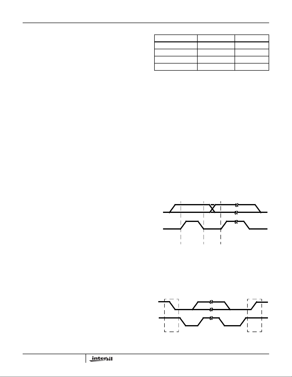
TABL E 1 .
2
C BITS SEL18V (1, 2) O/P VOLTAGE
I
13V Low 13V
14V Low 14V
13V High 18V
14V High 19V
I2C Bus Interface for ISL6405
(Refer to Philips I2C Specification, Rev. 2.1)
Data transmission from main microprocessor to the ISL6405
and vice versa takes place through the two wire I
interface, consisting of the two lines SDA and SCL. Both SDA
and SCL are bidirectional lines, connected to a positive supply
voltage via a pull up resistor. (Pull up resistors to positive supply
voltage must be externally connected). When the bus is free,
both lines are HIGH. The output stages of ISL6405 will have an
open drain/open collector in order to perform the wired-AND
function. Data on the I
2
C bus can be transferred up to 100Kbps
in the standard-mode or up to 400Kbps in the fast-mode. The
level of logic “0” and logic “1” is dependent of associated value
of V
as per electrical specification table. One clock pulse is
DD
generated for each data bit transferred.
Data Validity
The data on the SDA line must be stable during the HIGH
period of the clock. The HIGH or LOW state of the data line
can only change when the clock signal on the SCL line is
LOW. Refer to Figure 1.
SDA
SCL
DATA LINE
STABLE
DATA VALID
FIGURE 1. DATA VALIDITY
CHANGE
OF DATA
ALLOWED
START and STOP Conditions
As shown in Figure 2, START condition is a HIGH to LOW
transition of the SDA line while SCL is HIGH.
The STOP condition is a LOW to HIGH transition on the SDA
line while SCL is HIGH. A STOP condition must be sent
before each START condition.
SDA
2
C bus
External Output Voltage Selection
The output voltage can be selected by the I2C bus.
Additionally, the QFN package offers two pins (SEL18V1,
SEL18V2) for independent 13V/18V output voltage
selection. When using these pins, the I
2
C bits should be
initialized to 13V status.
8
SCL
CONDITION
SP
START
FIGURE 2. START AND STOP WAVEFORMS
STOP
CONDITION
Page 9
ISL6405
www.BDTIC.com/Intersil
Byte Format
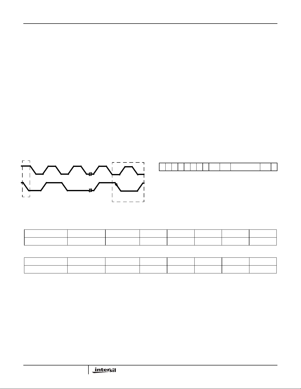
Every byte put on the SDA line must be eight bits long. The
number of bytes that can be transmitted per transfer is
unrestricted. Each byte has to be followed by an
acknowledge bit. Data is transferred with the most significant
bit first (MSB).
Acknowledge
The master (microprocessor) puts a resistive HIGH level on
the SDA line during the acknowledge clock pulse (Figure 3).
The peripheral that acknowledges has to pull down (LOW)
the SDA line during the acknowledge clock pulse, so that the
SDA line is stable LOW during this clock pulse. (Of course,
set-up and hold times must also be taken into account.)
The peripheral which has been addressed has to generate
an acknowledge after the reception of each byte, otherwise
the SDA line remains at the HIGH level during the ninth
clock pulse time. In this case, the master transmitter can
generate the STOP information in order to abort the transfer.
The ISL6405 will not generate the acknowledge if the
POWER OK signal from the UVLO is LOW.
SCL
1
2
8
9
Transmission Without Acknowledge
Avoiding detection of the acknowledgement, the
microprocessor can use a simpler transmission; it waits one
clock without checking the slave acknowledging, and sends
the new data.
This approach, though, is less protected from error and
decreases the noise immunity.
ISL6405 Software Description
Interface Protocol
The interface protocol is comprised of the following, as
shown below in Table 2:
• A start condition (S)
• A chip address byte (MSB on left; the LSB bit determines
read (1) or write (0) transmission) (the assigned I
address for the ISL6405 is 0001 00XX)
• A sequence of data (1 byte + Acknowledge)
• A stop condition (P)
TABLE 2. INTERFACE PROTOCOL
S0001000R/WACK Data (8 bits) ACKP
2
C slave
SDA
START
System Register Format
MSB
ACKNOWLEDGE
FROM SLAVE
FIGURE 3. ACKNOWLEDGE ON THE I2C BUS
TABLE 3. SYSTEM REGISTER 1 (SR1)
R, W R, W R, W R, W R, W R, W R, W R
SR1 DCL ISEL1 ENT1 LLC1 VSEL1 EN1 OLF1
TABLE 4. SYSTEM REGISTER 2 (SR2)
R, W R, W R, W R, W R, W R, W R R
SR2 ISEL2 ENT2 LLC2 VSEL2 EN2 OTF OLF2
• R, W = Read and Write bit
• R = Read-only bit
All bits reset to 0 at Power-On
9
Page 10
ISL6405
www.BDTIC.com/Intersil
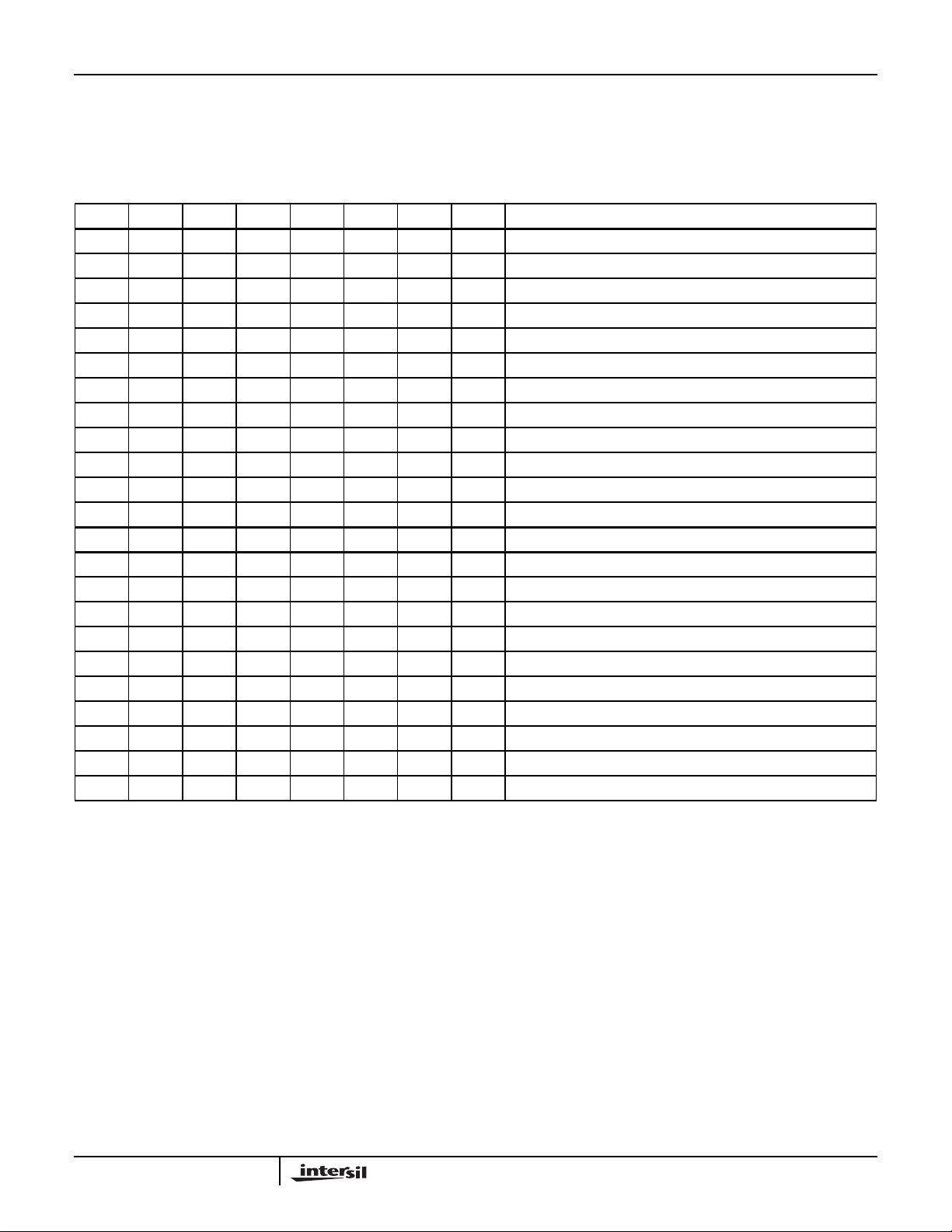
Transmitted Data (I
When the R/W bit in the chip is set to 0, the main
microprocessor can write on the system registers (SR1/SR2)
of the ISL6405 via I
SR DCL ISEL1 ENT1 LLC1 VSEL1 EN1 OLF1 FUNCTION
0 0 0 1 SR1 is selected
0 0 0 1 Vout1 = 13V, Vboost1 = 13V + Vdrop
0 0 1 1 Vout1 = 18V, Vboost1 = 18V + Vdrop
0 1 0 1 Vout1 = 14V, Vboost1 = 14V + Vdrop
0 1 1 1 Vout1 = 19V, Vboost1 = 19V + Vdrop
0 0 1 22kHz tone is controlled by DSQIN1 pin
0 1 1 22kHz tone is ON, DSQIN1 is disabled
0 0 1 Iout1 = 425mA max.
0 1 1 Iout1 = 775mA max.
0 1 1 Dynamic current limit NOT selected
0 0 1 Dynamic current limit selected
0 X X X X X 0 PWM and Linear for channel 1 disabled
SR ISEL2 ENT2 LLC2 VSEL2 EN2 OTF OLF2 FUNCTION
1 X X SR2 is selected
1 0 0 1 X X Vout2 = 13V, Vboost2 = 13V + Vdrop
1 0 1 1 X X Vout2 = 18V, Vboost2 = 18V + Vdrop
1 1 0 1 X X Vout2 = 14V, Vboost2 = 14V + Vdrop
1 1 1 1 X X Vout2 = 19V, Vboost2 = 19V + Vdrop
1 0 X X 22kHz tone is controlled by DSQIN2 pin
1 1 X X 22kHz tone is ON, DSQIN2 is disabled
1 0 X X Iout2 = 425mA max.
1 1 X X Iout2 = 775mA max.
1 X X X X 0 X X PWM and Linear for channel 2 disabled
2
C bus WRITE mode)
2
C bus. These will be written by the
TABLE 5. SYSTEM REGISTER (SR1 AND SR2) CONFIGURATION
microprocessor as shown below. The spare bits of SR1/SR2
can be used for other functions.
10
Page 11
ISL6405
www.BDTIC.com/Intersil
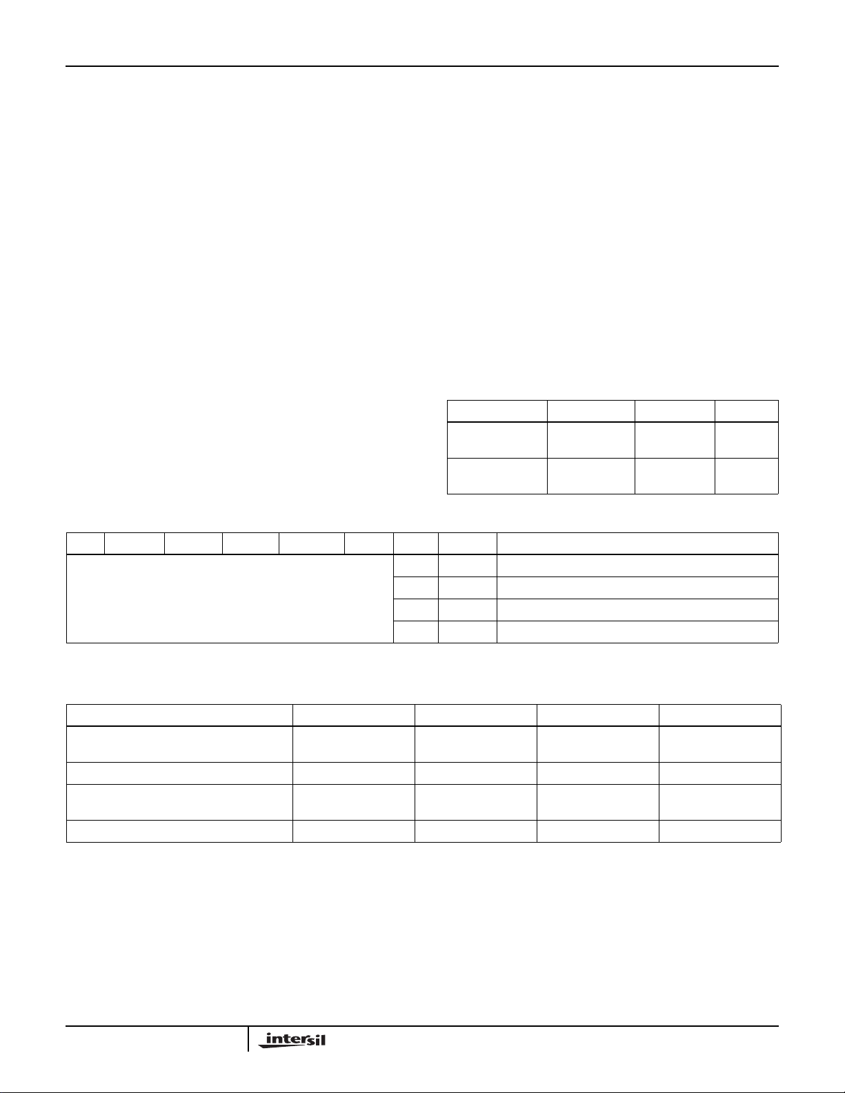
Received Data (I
2
C bus READ MODE)
The ISL6405 can provide to the master a copy of the system
register information via the I
2
C bus in read mode. The read
mode is Master activated by sending the chip address with
R/W bit set to 1. At the following Master generated clock bits,
the ISL6405 issues a byte on the SDA data bus line (MSB
transmitted first).
At the ninth clock bit the MCU master can:
• Acknowledge the reception, starting in this way the
transmission of another byte from the ISL6405.
• Not acknowledge, stopping the read mode
communication.
While the whole register is read back by the microprocessor,
only the two read-only bits, OLF and OTF, convey diagnostic
information about the ISL6405.
After selection of SR1/SR2 ?
Power–On I2C Interface Reset
The I2C interface built into the ISL6405 is automatically reset
at power-on. The I
logic signal from the UVLO circuit. This signal will go HIGH
2
C interface block will receive a Power OK
when chip power is OK. As long as this signal is LOW, the
interface will not respond to any I
2
C commands and the
system register SR1 and SR2 are initialized to all zeros, thus
keeping the power blocks disabled. Once the Vcc rises
above UVLO, the POWER OK signal given to the I
interface block will be HIGH, the I
2
C interface becomes
2
C
operative and the SRs can be configured by the main
microprocessor. About 400mV of hysteresis is provided in
the UVLO threshold to avoid false triggering of the PowerOn reset circuit. (I
at the same time as (or later than) all other I
2
C comes up with EN = 0; EN goes HIGH
2
C data for that
PWM becomes valid).
ADDRESS Pin
Connecting this pin to GND the chip I2C interface address is
0001000, but, it is possible to choose between two different
addresses simply by setting this pin at one of the two fixed
voltage levels as shown in Table 8.
TABLE 6. ADDRESS PIN CHARACTERISTICS
V
ADDR
-1
V
ADDR
“0001000”
V
-2
ADDR
“0001001”
MINIMUM TYPICAL MAXIMUM
0V - 2V
2.7V - 5V
TABLE 7. READING SYSTEM REGISTERS
DCL ISEL1/2 ENT1/2 LLC1/2 VSEL1/1 EN1/2 OTF2 OLF1/2 FUNCTION
These bits are read as they were after the last write operation. 0 T
1T
0I
1I
≤ 130°C, normal operation
J
> 150°C, power blocks disabled
J
< I
OUT
OUT
, normal operation
MAX
> I
, overload protection triggered
MAX
I2C Electrical Characteristics
TABLE 8. I2C SPECIFICATIONS
PARAMETER TEST CONDITION MINIMUM TYPICAL MAXIMUM
Input Logic High, VIH SDA, SCL 0.7 x V
Input Logic Low, VIL SDA, SCL 0.3 x V
Input Logic Current, IIL SDA, SCL;
0.4V < V
SCL Clock Frequency 0 100kHz 400kHz
IN
< 4.5V
DD
DD
10µA
11
Page 12
ISL6405
www.BDTIC.com/Intersil
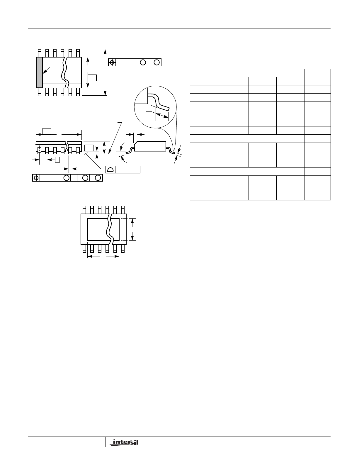
Small Outline Exposed Pad Plastic Packages (EPSOIC)
N
INDEX
AREA
123
TOP VIEW
-AD
e
B
0.25(0.010) C AM BS
SIDE VIEW
123
N
H
E
-B-
SEATING PLANE
A
-C-
A1
M
P
BOTTOM VIEW
0.25(0.010) BM M
L
h x 45
α
0.10(0.004)
P1
M28.3B
28 LEAD WIDE BODY SMALL OUTLINE EXPOSED PAD
PLASTIC PACKAGE
INCHES
SYMBOL
A 0.091 - 0.099 -
A1 0.001 - 0.005 -
B 0.014 - 0.019 9
C 0.0091 - 0.0125 -
D 0.701 - 0.711 3
o
C
E 0.292 - 0.299 4
e 0.050 BSC -
H 0.400 - 0.410 -
h 0.010 - 0.016 5
L 0.024 - 0.040 6
N287
α
P 0.180 0.214 0.218 11
P1 0.156 0.190 0.194 11
NOTES:
1. Symbols are defined in the “MO Series Symbol List” in Section
2.2 of Publication Number 95.
2. Dimensioning and tolerancing per ANSI Y14.5M-1982.
3. Dimension “D” does not include mold flash, protrusions or gate
burrs. Mold flash, protrusion and gate burrs shall not exceed
0.15mm (0.006 inch) per side.
4. Dimension “E” does not include interlead flash or protrusions.
Interlead flash and protrusions shall not exceed 0.25mm (0.010
inch) per side.
5. The chamfer on the body is optional. If it is not present, a visual
index feature must be located within the crosshatched area.
6. “L” is the length of terminal for soldering to a substrate.
7. “N” is the number of terminal positions.
8. Terminal numbers are shown for reference only.
9. The lead width “B”, as measured 0.36mm (0.014 inch) or greater
above the seating plane, shall not exceed a maximum value of
0.61mm (0.024 inch)
10. Controlling dimension: INCH.
11. Dimensions “P” and “P1” are thermal and/or electrical enhanced
variations. Values shown are maximum size of exposed pad
within lead count body size.
0° 5° 8° -
NOTESMIN NOMINAL MAX
Rev. 0 5/02
12
Page 13
ISL6405
www.BDTIC.com/Intersil
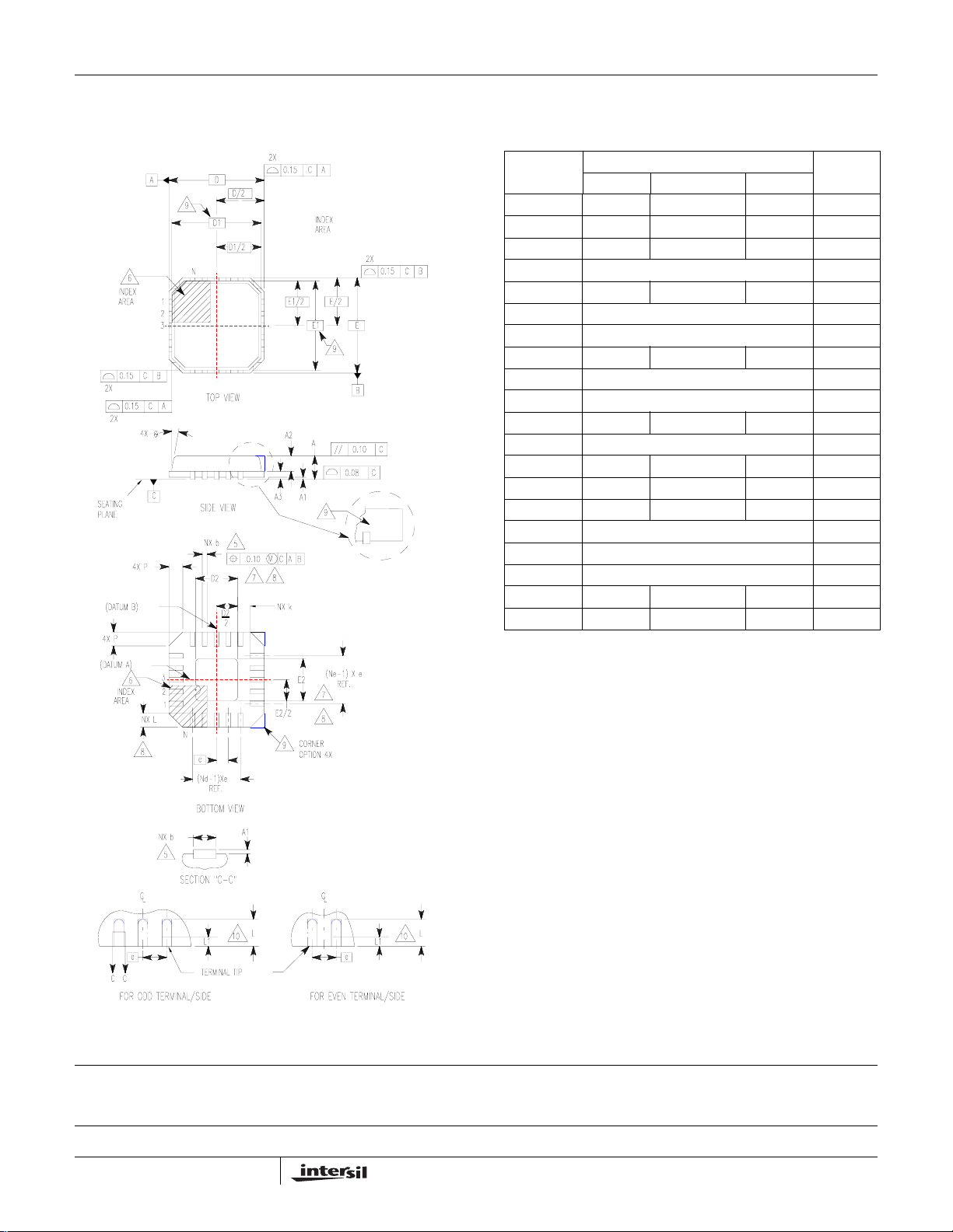
Quad Flat No-Lead Plastic Package (QFN)
Micro Lead Frame Plastic Package (MLFP)
L32.5x5
32 LEAD QUAD FLAT NO-LEAD PLASTIC PACKAGE
(COMPLIANT TO JEDEC MO-220VHHD-2 ISSUE C
MILLIMETERS
SYMBOL
A 0.80 0.90 1.00 A1 - - 0.05 A2 - - 1.00 9
A3 0.20 REF 9
b 0.18 0.23 0.30 5,8
D 5.00 BSC D1 4.75 BSC 9
D2 2.95 3.10 3.25 7,8
E 5.00 BSC E1 4.75 BSC 9
E2 2.95 3.10 3.25 7,8
e 0.50 BSC -
k0.25 - - -
L 0.30 0.40 0.50 8
L1 - - 0.15 10
N322
Nd 8 3
Ne 8 8 3
P- -0.609
θ --129
NOTES:
1. Dimensioning and tolerancing conform to ASME Y14.5-1994.
2. N is the number of terminals.
3. Nd and Ne refer to the number of terminals on each D and E.
4. All dimensions are in millimeters. Angles are in degrees.
5. Dimension b applies to the metallized terminal and is measured
between 0.15mm and 0.30mm from the terminal tip.
6. The configuration of the pin #1 identifier is optional, but must be
located within the zone indicated. The pin #1 identifier may be
either a mold or mark feature.
7. Dimensions D2 and E2 are for the exposed pads which provide
improved electrical and thermal performance.
8. Nominal dimensions are provided to assist with PCB Land Pattern
Design efforts, see Intersil Technical Brief TB389.
9. Features and dimensions A2, A3, D1, E1, P & θ are present when
Anvil singulation method is used and not present for saw
singulation.
10. Depending on the method of lead termination at the edge of the
package, a maximum 0.15mm pull back (L1) maybe present. L
minus L1 to be equal to or greater than 0.3mm.
NOTESMIN NOMINAL MAX
Rev. 1 10/02
All Intersil U.S. products are manufactured, assembled and tested utilizing ISO9000 quality systems.
Intersil Corporation’s quality certifications can be viewed at www.intersil.com/design/quality
Intersil products are sold by description only. Intersil Corporation reserves the right to make changes in circuit design, software and/or specifications at any time without
notice. Accordingly, the reader is cautioned to verify that data sheets are current before placing orders. Information furnished by Intersil is believed to be accurate and
reliable. However, no responsibility is assumed by Intersil or its subsidiaries for its use; nor for any infringements of patents or other rights of third parties which may result
from its use. No license is granted by implication or otherwise under any patent or patent rights of Intersil or its subsidiaries.
For information regarding Intersil Corporation and its products, see www.intersil.com
13
 Loading...