

Page 1

Dual 4-Phase + 1-Phase PWM Controller for VR12/IMVP7
Applications
ISL6364
The ISL6364 is a dual PWM controller; its 4-phase PWMs control
the microprocessor core or the memory voltage regulator, while
its single-phase PWM controls the peripheral voltage regulator
for graphics, system agent, or processor I/O.
The ISL6364 utilizes Intersil’s proprietary Enhanced Active Pulse
Positioning (EAPP) modulation scheme to achieve the extremely
fast transient response with fewer output capacitors.
The ISL6364 is designed to be compliant to Intel VR12/IMVP7
specifications. It accurately monitors the load current via the
IMON pin and reports this information via the IOUT register to
the microprocessor, which sends a PSI# signal to the controller
at low power mode via SVID bus. The controller enters 1- or
2-phase operation in low power mode (PSI1); in the ultra low
power mode (PSI2,3), it can further drop the number of phases
and then enable the diode emulation of the operational phase.
In low power modes, the magnetic core and switching losses are
significantly reduced, yielding high efficiency at light load. After
the PSI# signal is de-asserted, the dropped phase(s) are added
back to sustain heavy load transient response and efficiency.
Today’s microprocessors require a tightly regulated output voltage
position versus load current (droop). The ISL6364 senses the
output current continuously by measuring the voltage across the
dedicated current sense resistor or the DCR of the output
inductor. The sensed current flows out of the FB pin to develop the
precision voltage drop across the feedback resistor for droop
control. Current sensing circuits also provide the needed signals
for channel-current balancing, average overcurrent protection and
individual phase current limiting. The TM and TMS pins are to
sense an NTC thermistor’s temperature, which is internally
digitized for thermal monitoring and for integrated thermal
compensation of the current sense elements of the respective
regulator.
The ISL6364 features remote voltage sensing and completely
eliminates any potential difference between remote and local
grounds. This improves regulation and protection accuracy. The
threshold-sensitive enable input is available to accurately
coordinate the start-up of the ISL6364 with other voltage rails.
Features
• Intel VR12/IMVP7 Compliant
- SerialVID with Programmable IMAX, TMAX, BOOT,
ADDRESS OFFSET Registers
• Intersil’s Proprietary Enhanced Active Pulse Positioning
(EAPP) Modulation Scheme, Patented
- Voltage Feed-forward and Ramp Adjustable Options
- High Frequency and PSI Compensation Options
- Variable Frequency Control During Load Transients to
Reduce Beat Frequency Oscillation
- Linear Control with Evenly Distributed PWM Pulses for
Better Phase Current Balance During Load Transients
•Dual Outputs
- Output 1 (VR0): 1 to 4-Phase, Coupled Inductor
Compatibility, for Core or Memory
- Output 2 (VR1): Single Phase for Graphics, System Agent,
or Processor I/O
- Differential Remote Voltage Sensing
- ±0.5% Closed-loop System Accuracy Over Load, Line and
Temper ature
- Phase Doubler Compatibility (NOT Phase Dropping)
• Proprietary Active Phase Adding and Dropping with Diode
Emulation Scheme For Enhanced Light Load Efficiency
•Programmable Slew Rate of Fast Dynamic VID for VR0
• Dynamic VID Compensation (DVS) for VR1 at No Droop
• Droop and Diode Emulation Options
• Programmable 1 or 2-Phase Operation in PSI1/2/3 Mode
• Programmable Standard or Coupled-Inductor Operation
• Precision Resistor
- Integrated Programmable Current Sense Resistors
- Integrated Thermal Compensation
- Accurate Load-Line (Droop) Programming
- Accurate Channel-Current Balancing
- Accurate Current Monitoring
• Average Overcurrent Protection and Channel Current Limit
With Internal Current Comparators
• Precision Overcurrent Protection on IMON & IMONS Pins
• Independent Oscillators, up to 1MHz Per Phase, for Cost,
Efficiency, and Performance Optimization
• Dual Thermal Monitoring and Thermal Compensation
• Start-up Into Pre-Charged Load
• Pb-Free (RoHS Compliant)
or DCR Differential Current Sensing
December 22, 2010
FN6861.0
1
CAUTION: These devices are sensitive to electrostatic discharge; follow proper IC Handling Procedures.
1-888-INTERSIL or 1-888-468-3774
Intersil (and design) is a trademark owned by Intersil Corporation or one of its subsidiaries.
All other trademarks mentioned are the property of their respective owners.
|Copyright Intersil Americas Inc. 2010. All Rights Reserved
Page 2
Ordering Information
ISL6364
PART NUMBER
(Notes 1, 2, 3)
PART
MARKING
TEMP. RANGE
(°C)
PACKAGE
(Pb-Free)
PKG.
DWG. #
ISL6364CRZ ISL6364 CRZ 0 to +70 48 Ld 6x6 QFN L48.6x6B
ISL6364IRZ ISL6364 IRZ -40 to +85 48 Ld 6x6 QFN L48.6x6B
NOTES:
1. Add “-T*” suffix for tape and reel. Please refer to TB347 for details on reel specifications.
2. These Intersil Pb-free plastic packaged products employ special Pb-free material sets, molding compounds/die attach materials, and 100% matte
tin plate plus anneal (e3 termination finish, which is RoHS compliant and compatible with both SnPb and Pb-free soldering operations). Intersil Pbfree products are MSL classified at Pb-free peak reflow temperatures that meet or exceed the Pb-free requirements of IPC/JEDEC J STD-020.
3. For Moisture Sensitivity Level (MSL), please see device information page for ISL6364
. For more information on MSL please see techbrief TB363.
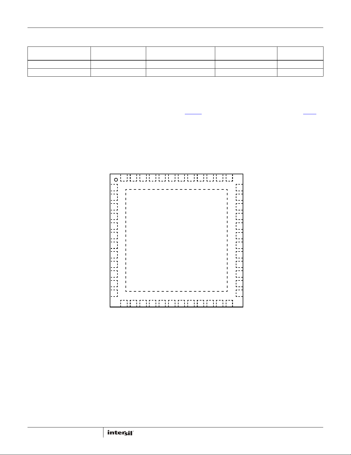
Pin Configuration
ISL6364
(48 LD 6X6 QFN)
TOP VIEW
ISEN3+
ISEN3-
ISEN1+
ISEN1-
ISEN4+
ISEN4-
ISEN2+
ISEN2-
EN_VTT
PWM3
PWM1
PWM4
48 47 46 45 44 43 42 41 40 39 38 37
EN_PWR
RAMP_ADJ
RGND
VSEN
HFCOMP
PSICOMP
FB
COMP
IMON
SVDATA
SVALERT#
SVCLK
1
2
3
4
5
6
7
8
9
10
11
12
GND
36
PWM2
35
VCC
34
FS_DRP
33
RSET
SICI
32
TM
31
30
BTS_DES_TCOMPS
29
BT_FDVID_TCOMP
28
NPSI_DE_IMAX
27
ADDR_IMAXS_TMAX
26
PWMS
25
ISENS-
13 14 15 16 17 18 19 20 21 22 23 24
IMONS
VR_RDY
VR_HOT#
VR_RDYS
HFCOMPS/DVCS
FBS
VSENS
COMPS
RGNDS
2
TMS
ISENS+
FSS_DRPS
FN6861.0
December 22, 2010
Page 3

ISL6364
Controller and Driver Recommendation
GATE
QUIESCENT
DRIVER
ISL6627 1.0 5V Single Yes No For PSI# channel and its coupled channel in
ISL6620
ISL6620A
ISL6596 0.19 5V Single No No For dropped phases or all channels without DE
ISL6610
ISL6610A
ISL6611A 1.25 5V Dual No No Phase Doubler with Integrated Drivers, up to 12-
ISL6617 5.0 N/A N/A No No PWM Doubler for DrMOS, up to 12 or 24-Phase.
ISL6625 1.2 12V Single Yes Yes For PSI# channel and its coupled channel in
ISL6622 5.5 12V Single Yes Yes For PSI# channel and its coupled channel in
ISL6622A
ISL6622B
ISL6625A 1.0 12V Single No No For dropped phases or all channels without DE
NOTE: Intersil 5V and 12V drivers are mostly pin-to-pin compatible and allow for dual footprint layout implementation to optimize MOSFET selection and
efficiency. 5V Drivers are more suitable for high frequency and high efficiency applications.
CURRENT (mA)
1.2 5V Single Yes No For PSI# channel and its coupled channel in
0.24 5V Dual No No For dropped phases or all channels without DE
5.5 12V Single Yes No For PSI# channel and its coupled channel in
DRIVE
VOLTAGE
# OF
DRIVERS
DIODE EMULATION
(DE)
GATE DRIVE
DROP
(GVOT) COMMENTS
coupled inductor applications or all channels
coupled inductor applications or all channels.
Shorter body diode conduction time when enters
PSI2 mode at a fixed voltage.
Phase. For all channels with DE Disabled
For all channels with DE Disabled
coupled inductor applications or all channels
coupled inductor applications or all channels.
Shorter body diode conduction time when enters
PSI2 mode at a fixed voltage.
coupled inductor applications or all channels.
Shorter body diode conduction time when enters
PSI2 mode at a fixed voltage.
3
FN6861.0
December 22, 2010
Page 4
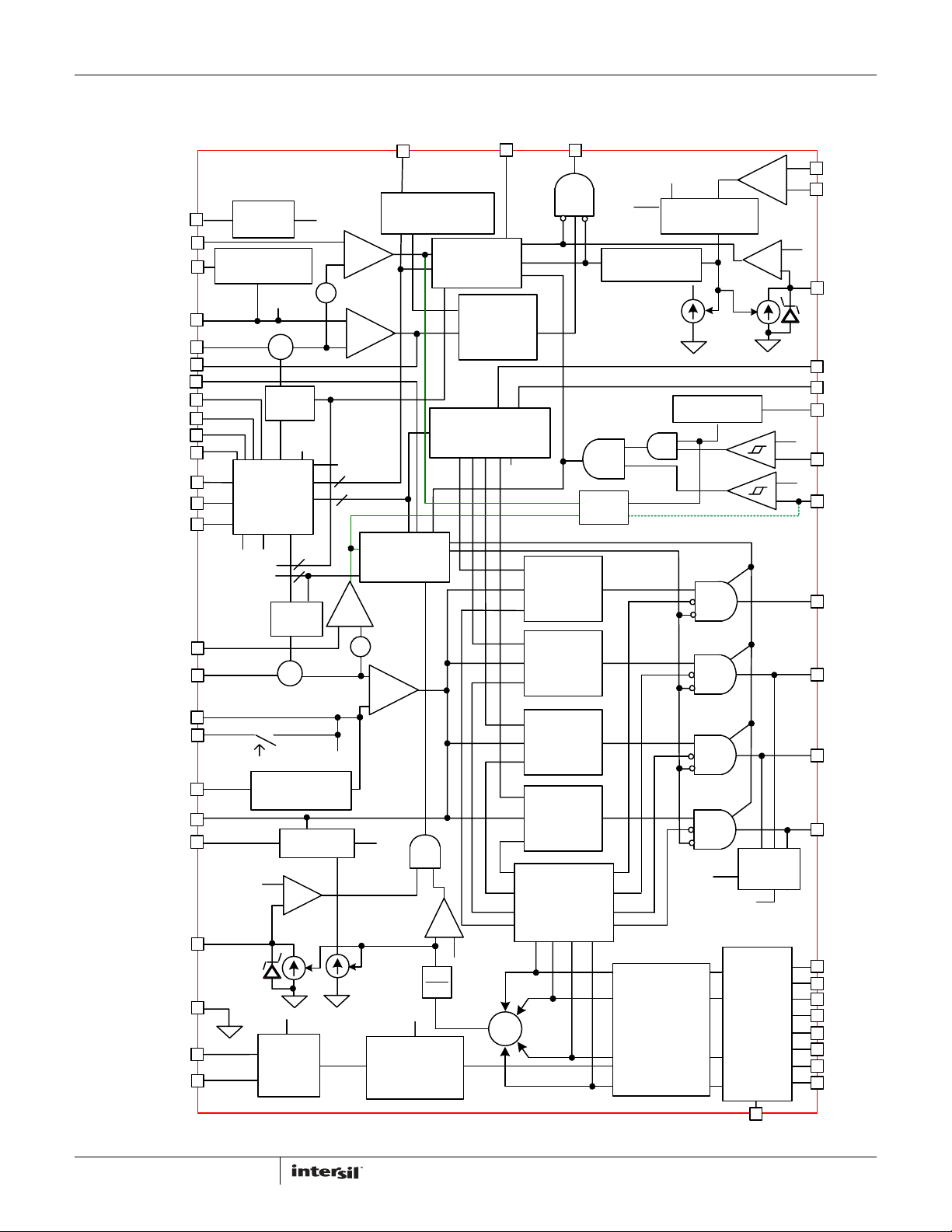
ISL6364
ISL6364 Internal Block Diagram
TMS
VSENS
HFCOMPS/DVCS
FBS
RGNDS
COMPS
VR_RDY
BTS_DES_TCOMPS
BT_FDVID_TCOMP
NPSI_DE_IMAX
ADDR_IMAXS_TMAX
SVCLK
SVALERT#
SVDATA
VSEN
RGND
PSICOMP
HFCOMP
COMP
SICI
“SICI” FOR
ISL6364:
“IAUTO” FOR
ISL6364A
IMON
GND
VR_HOT#
FB
TM
THERMAL
MONITOR
HIGH FREQUENCY
COMPENSATION
SVID BUS
INTERFACE
TCOMP
PSI#
HIGH FREQUENCY
1.11V
1.15V
IDROOPS
+
+
DAC &
OFFSET
TCOMPS
PSI#
DAC &
OFFSET
+
REF
+
IDROOP
COMPENSATION
AUTO PHASE
SHEDDING
+
OCP
-
TMAX
THERMAL
MONITOR
THGS
+
-
THG
+
OVP
-
175mV
+
E/A
-
TMAX
VR1 REGs
VR0 REGs
OVP
-
+
+
-
SHED
IDROOP
FSS_DRPS
VR1: CLOCK AND
RAMP GENERATOR
SOFT-START
AND
FAULT LOGIC
175mV
+
E/A
-
-
TCOMP
TEMPERATURE
COMPENSATION
GAIN ADJ UST
VR_RDYS
SOFT-START
AND
FAULT LOGIC
EAPP
MODULATOR
VR0: CLOCK AND
RAMP GENERATOR
OCP
+
I_TRIP
1
N
N
MODULATOR
MODULATOR
MODULATOR
MODULATOR
CURRENT LIMIT
Σ
PWMS
EAPP
EAPP
EAPP
EAPP
CHANNEL
CURRENT
BALANCE
AND PEAK
THGS
AVERAGE & PEAK
CURRENT LIMIT
LATCH
TEMPERATURE
COMPENSATION
TCOMPS
IDROOPS
RESET
TEMPERATURE
COMPENSATION
POWER-ON
RESET (POR)
SHED
CHANNEL
CURRENT
E/A
OCP
+
CHANNEL
DETECT
N
SENSE
-
ISENS+
+
ISENS-
1.11V
-
+
IMONS
1.15V
FS_DRP
RAMP_ADJ
VCC
0.85V
-
EN_VTT
0.85V
-
+
EN_PWR_OVP
OVP FOR
ISL6364A
PWM1
PWM2
PWM3
PWM4
ISEN1+
ISEN1-
ISEN2+
ISEN2-
ISEN3+
ISEN3-
ISEN4+
ISEN4-
RSET
4
FN6861.0
December 22, 2010
Page 5
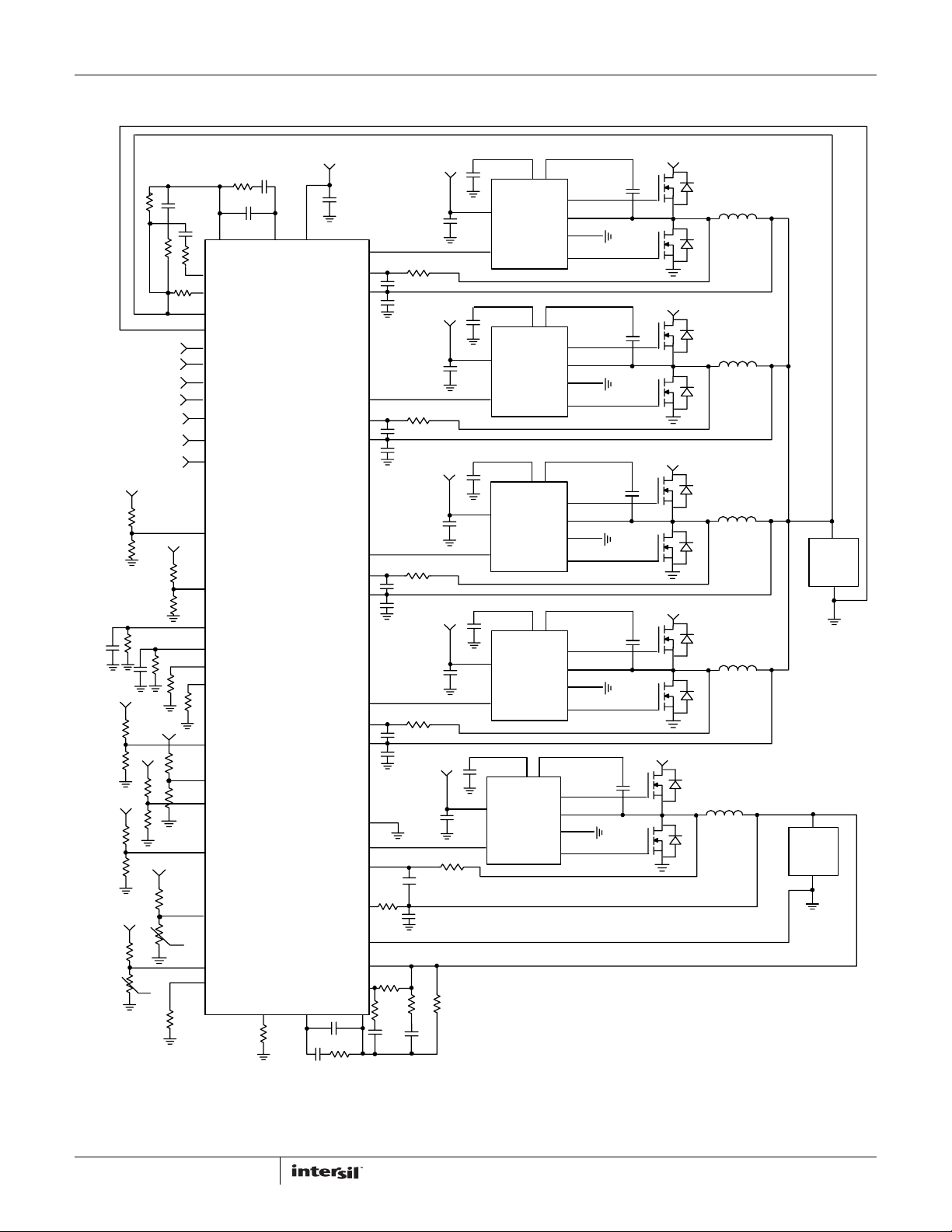
ISL6364
Typical Application: 4-Phase VR and 1-Phase VR WITH ISL6364
SVALERT#
SVDATA
SVCLK
VR_RDY
VR_RDYS
VR_HOT#
VIN
+5V
+5V
+5V
+5V
VTT
+5V
PSICOMP
HFCOMP
VSEN
RGND
EN_VTT
EN_PWR_OVP
VIN
RAMP_ADJ
IMON
IMONS
FS_DRP
FSS_DRPS
BTS_DES_TCOMPS
BT_FDVID_TCOMP
ADDR_IMAXS_TMAX
NPSI_DE_IMAX
FB
ISL6364
VIN
VIN
VIN
VIN
VIN
GPU
LOAD
CPU
LOAD
+5V
VCCCOMP
PWM1
ISEN1-
ISEN1+
PWM2
ISEN2-
ISEN2+
PWM3
ISEN3-
ISEN3+
PWM4
ISEN4-
ISEN4+
GND
PWMS
ISENS-
+12V
+12V
+12V
+12V
+12V
VCC
PWM
VCC
PWM
VCC
PWM
VCC
PWM
VCC
PWM
PVCC
PVCC
PVCC
PVCC
PVCC
ISL6625
DRIVER
ISL6625
DRIVER
ISL6625
DRIVER
ISL6625
DRIVER
ISL6625
DRIVER
BOOT
UGATE
PHASE
GND
LGATE
BOOT
UGATE
PHASE
GND
LGATE
BOOT
UGATE
PHASE
GND
LGATE
BOOT
UGATE
PHASE
GND
LGATE
BOOT
UGATE
PHASE
GND
LGATE
+5V
NTC: Beta = ~ 3477
NTC
NTC
TMS
TM
SICI
HFCOMPS/DVCS
RSET
COMPS
5
ISENS+
RGNDS
VSENS
FBS
FN6861.0
December 22, 2010
Page 6
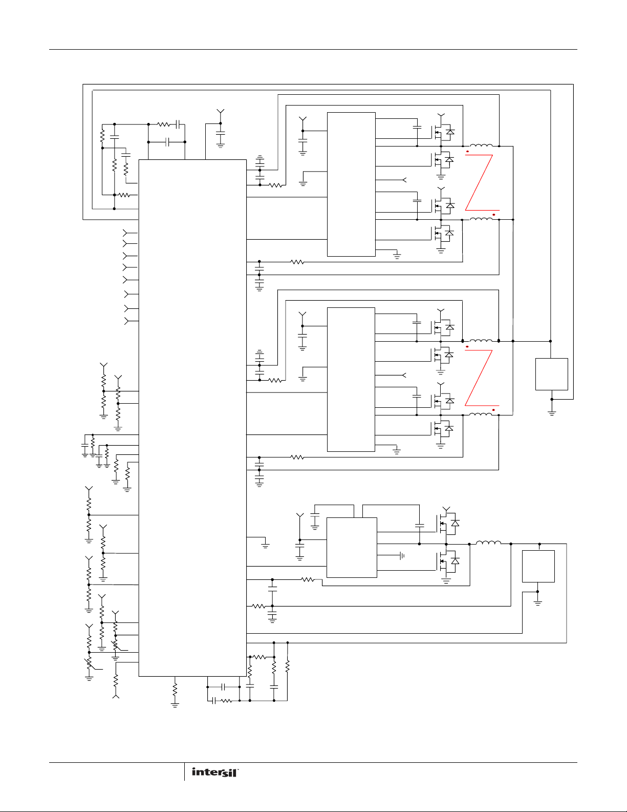
ISL6364
Typical Application: 4-Phase Coupled-Inductor VR and 1-Phase VR
VTT
SVALERT#
SVDATA
SVCLK
VR_RDY
VR_RDYS
VR_HOT#
OVP
VIN
+5V
VIN
FB
PSICOMP
HFCOMP
VSEN
RGND
EN_VTT
EN_PWR
RAMP_ADJ
IMON
IMONS
FS_DRP
FSS_DRPS
COMP
ISL6364
VCC
+5V
ISEN1+
ISEN1-
ISEN3-
ISEN3+
ISEN2+
ISEN2-
ISEN4-
ISEN4+
PWM1
PWM3
PWM2
PWM4
+5V
PWM1
PWM2
+5V
PWM1
PWM2
VCC
GND
VCC
GND
UGATE1
PHASE1
LGATE1
ISL6610
DRIVER
UGATE2
PHASE2
LGATE2
PGND
UGATE1
PHASE1
LGATE1
ISL6610
DRIVER
UGATE2
PHASE2
LGATE2
PGND
BOOT1
PVCC
BOOT2
BOOT1
PVCC
BOOT2
12V
12V
VIN
VIN
VIN
VIN
CPU
LOAD
+5V
+5V
+5V
+5V
+5V
NTC
NTC
+5V
NTC: BETA = ~ 3477
BTS_DES_TCOMPS
ADDR_IMAXS_TMAX
NPSI_DE_IMAX
BT_FDVID_TCOMP
TMS
TM
SICI
HFCOMPS/DVCS
RSET
COMPS
6
GND
PWMS
ISENS-
ISENS+
RGNDS
VSENS
FBS
+12V
VCC
PWM
PVCC
ISL6625
DRIVER
BOOT
UGATE
PHASE
GND
LGATE
VIN
GPU
LOAD
FN6861.0
December 22, 2010
Page 7

ISL6364
Table of Contents
Absolute Maximum Ratings. . . . . . . . . . . . . . . . . . . . . . . . . . . . . . . . . . . . . . . . . . . . . . . . . . . . . . . . . . . . . . . . . . . . . . . . . . . . . . . . . . . . . . . . . . . 8
Thermal Information . . . . . . . . . . . . . . . . . . . . . . . . . . . . . . . . . . . . . . . . . . . . . . . . . . . . . . . . . . . . . . . . . . . . . . . . . . . . . . . . . . . . . . . . . . . . . . . . . 8
Recommended Operating Conditions. . . . . . . . . . . . . . . . . . . . . . . . . . . . . . . . . . . . . . . . . . . . . . . . . . . . . . . . . . . . . . . . . . . . . . . . . . . . . . . . . . . 8
Electrical Specifications . . . . . . . . . . . . . . . . . . . . . . . . . . . . . . . . . . . . . . . . . . . . . . . . . . . . . . . . . . . . . . . . . . . . . . . . . . . . . . . . . . . . . . . . . . . . . . . . . . . . . . . .8
Typical Performance Curves. . . . . . . . . . . . . . . . . . . . . . . . . . . . . . . . . . . . . . . . . . . . . . . . . . . . . . . . . . . . . . . . . . . . . . . . . . . . . . . . . . . . . . . . . . 10
Functional Pin Descriptions . . . . . . . . . . . . . . . . . . . . . . . . . . . . . . . . . . . . . . . . . . . . . . . . . . . . . . . . . . . . . . . . . . . . . . . . . . . . . . . . . . . . . . . . . . 11
Operation . . . . . . . . . . . . . . . . . . . . . . . . . . . . . . . . . . . . . . . . . . . . . . . . . . . . . . . . . . . . . . . . . . . . . . . . . . . . . . . . . . . . . . . . . . . . . . . . . . . . . . . . . 13
Multiphase Power Conversion . . . . . . . . . . . . . . . . . . . . . . . . . . . . . . . . . . . . . . . . . . . . . . . . . . . . . . . . . . . . . . . . . . . . . . . . . . . . . . . . . . . . . 13
Interleaving. . . . . . . . . . . . . . . . . . . . . . . . . . . . . . . . . . . . . . . . . . . . . . . . . . . . . . . . . . . . . . . . . . . . . . . . . . . . . . . . . . . . . . . . . . . . . . . . . . . . . 13
PWM Modulation Scheme . . . . . . . . . . . . . . . . . . . . . . . . . . . . . . . . . . . . . . . . . . . . . . . . . . . . . . . . . . . . . . . . . . . . . . . . . . . . . . . . . . . . . . . . 14
PWM and PSI# Operation. . . . . . . . . . . . . . . . . . . . . . . . . . . . . . . . . . . . . . . . . . . . . . . . . . . . . . . . . . . . . . . . . . . . . . . . . . . . . . . . . . . . . . . . . 15
Diode Emulation Operation . . . . . . . . . . . . . . . . . . . . . . . . . . . . . . . . . . . . . . . . . . . . . . . . . . . . . . . . . . . . . . . . . . . . . . . . . . . . . . . . . . . . . . . 16
Switching Frequency . . . . . . . . . . . . . . . . . . . . . . . . . . . . . . . . . . . . . . . . . . . . . . . . . . . . . . . . . . . . . . . . . . . . . . . . . . . . . . . . . . . . . . . . . . . . . 16
Current Sensing . . . . . . . . . . . . . . . . . . . . . . . . . . . . . . . . . . . . . . . . . . . . . . . . . . . . . . . . . . . . . . . . . . . . . . . . . . . . . . . . . . . . . . . . . . . . . . . . . 16
Channel-Current Balance for VR0 . . . . . . . . . . . . . . . . . . . . . . . . . . . . . . . . . . . . . . . . . . . . . . . . . . . . . . . . . . . . . . . . . . . . . . . . . . . . . . . . . . 19
Voltage Regulation . . . . . . . . . . . . . . . . . . . . . . . . . . . . . . . . . . . . . . . . . . . . . . . . . . . . . . . . . . . . . . . . . . . . . . . . . . . . . . . . . . . . . . . . . . . . . . 19
Load-Line Regulation . . . . . . . . . . . . . . . . . . . . . . . . . . . . . . . . . . . . . . . . . . . . . . . . . . . . . . . . . . . . . . . . . . . . . . . . . . . . . . . . . . . . . . . . . . . . 26
Output-Voltage Offset Programming. . . . . . . . . . . . . . . . . . . . . . . . . . . . . . . . . . . . . . . . . . . . . . . . . . . . . . . . . . . . . . . . . . . . . . . . . . . . . . . . 27
Dynamic VID . . . . . . . . . . . . . . . . . . . . . . . . . . . . . . . . . . . . . . . . . . . . . . . . . . . . . . . . . . . . . . . . . . . . . . . . . . . . . . . . . . . . . . . . . . . . . . . . . . . . 27
Operation Initialization . . . . . . . . . . . . . . . . . . . . . . . . . . . . . . . . . . . . . . . . . . . . . . . . . . . . . . . . . . . . . . . . . . . . . . . . . . . . . . . . . . . . . . . . . . . . . . 27
Enable and Disable . . . . . . . . . . . . . . . . . . . . . . . . . . . . . . . . . . . . . . . . . . . . . . . . . . . . . . . . . . . . . . . . . . . . . . . . . . . . . . . . . . . . . . . . . . . . . . 27
Soft-Start. . . . . . . . . . . . . . . . . . . . . . . . . . . . . . . . . . . . . . . . . . . . . . . . . . . . . . . . . . . . . . . . . . . . . . . . . . . . . . . . . . . . . . . . . . . . . . . . . . . . . . . 28
Current Sense Output . . . . . . . . . . . . . . . . . . . . . . . . . . . . . . . . . . . . . . . . . . . . . . . . . . . . . . . . . . . . . . . . . . . . . . . . . . . . . . . . . . . . . . . . . . . . . . . 28
Fault Monitoring and Protection . . . . . . . . . . . . . . . . . . . . . . . . . . . . . . . . . . . . . . . . . . . . . . . . . . . . . . . . . . . . . . . . . . . . . . . . . . . . . . . . . . . . . . 28
VR_Ready Signal . . . . . . . . . . . . . . . . . . . . . . . . . . . . . . . . . . . . . . . . . . . . . . . . . . . . . . . . . . . . . . . . . . . . . . . . . . . . . . . . . . . . . . . . . . . . . . . . 28
Overvoltage Protection . . . . . . . . . . . . . . . . . . . . . . . . . . . . . . . . . . . . . . . . . . . . . . . . . . . . . . . . . . . . . . . . . . . . . . . . . . . . . . . . . . . . . . . . . . . 28
Overcurrent Protection . . . . . . . . . . . . . . . . . . . . . . . . . . . . . . . . . . . . . . . . . . . . . . . . . . . . . . . . . . . . . . . . . . . . . . . . . . . . . . . . . . . . . . . . . . . 29
Thermal Monitoring (VR_HOT#) . . . . . . . . . . . . . . . . . . . . . . . . . . . . . . . . . . . . . . . . . . . . . . . . . . . . . . . . . . . . . . . . . . . . . . . . . . . . . . . . . . . . 29
Temperature Compensation . . . . . . . . . . . . . . . . . . . . . . . . . . . . . . . . . . . . . . . . . . . . . . . . . . . . . . . . . . . . . . . . . . . . . . . . . . . . . . . . . . . . . . . . . 31
Design Procedure . . . . . . . . . . . . . . . . . . . . . . . . . . . . . . . . . . . . . . . . . . . . . . . . . . . . . . . . . . . . . . . . . . . . . . . . . . . . . . . . . . . . . . . . . . . . . . . 31
External Temperature Compensation . . . . . . . . . . . . . . . . . . . . . . . . . . . . . . . . . . . . . . . . . . . . . . . . . . . . . . . . . . . . . . . . . . . . . . . . . . . . . . . 32
Hard-wired Registers (Patent Pending). . . . . . . . . . . . . . . . . . . . . . . . . . . . . . . . . . . . . . . . . . . . . . . . . . . . . . . . . . . . . . . . . . . . . . . . . . . . . . . . . 32
Dynamic VID Compensation (DVC) . . . . . . . . . . . . . . . . . . . . . . . . . . . . . . . . . . . . . . . . . . . . . . . . . . . . . . . . . . . . . . . . . . . . . . . . . . . . . . . . . . . . . . . . . . . . . 34
Disabling Output . . . . . . . . . . . . . . . . . . . . . . . . . . . . . . . . . . . . . . . . . . . . . . . . . . . . . . . . . . . . . . . . . . . . . . . . . . . . . . . . . . . . . . . . . . . . . . . . . . . 35
SVID Operation . . . . . . . . . . . . . . . . . . . . . . . . . . . . . . . . . . . . . . . . . . . . . . . . . . . . . . . . . . . . . . . . . . . . . . . . . . . . . . . . . . . . . . . . . . . . . . . . . . . . 35
General Design Guide . . . . . . . . . . . . . . . . . . . . . . . . . . . . . . . . . . . . . . . . . . . . . . . . . . . . . . . . . . . . . . . . . . . . . . . . . . . . . . . . . . . . . . . . . . . . . . . 35
Power Stages . . . . . . . . . . . . . . . . . . . . . . . . . . . . . . . . . . . . . . . . . . . . . . . . . . . . . . . . . . . . . . . . . . . . . . . . . . . . . . . . . . . . . . . . . . . . . . . . . . . 35
Current Sensing Resistor . . . . . . . . . . . . . . . . . . . . . . . . . . . . . . . . . . . . . . . . . . . . . . . . . . . . . . . . . . . . . . . . . . . . . . . . . . . . . . . . . . . . . . . . . 36
Load-Line Regulation Resistor . . . . . . . . . . . . . . . . . . . . . . . . . . . . . . . . . . . . . . . . . . . . . . . . . . . . . . . . . . . . . . . . . . . . . . . . . . . . . . . . . . . . . 36
Output Filter Design. . . . . . . . . . . . . . . . . . . . . . . . . . . . . . . . . . . . . . . . . . . . . . . . . . . . . . . . . . . . . . . . . . . . . . . . . . . . . . . . . . . . . . . . . . . . . . 37
Switching Frequency Selection . . . . . . . . . . . . . . . . . . . . . . . . . . . . . . . . . . . . . . . . . . . . . . . . . . . . . . . . . . . . . . . . . . . . . . . . . . . . . . . . . . . . 37
Input Capacitor Selection . . . . . . . . . . . . . . . . . . . . . . . . . . . . . . . . . . . . . . . . . . . . . . . . . . . . . . . . . . . . . . . . . . . . . . . . . . . . . . . . . . . . . . . . . 38
Layout and Design Considerations . . . . . . . . . . . . . . . . . . . . . . . . . . . . . . . . . . . . . . . . . . . . . . . . . . . . . . . . . . . . . . . . . . . . . . . . . . . . . . . . . . . . . . . . . . . . . 39
Pin Noise Sensitivity, Design and Layout Consideration. . . . . . . . . . . . . . . . . . . . . . . . . . . . . . . . . . . . . . . . . . . . . . . . . . . . . . . . . . . . . . . . 39
Component Placement . . . . . . . . . . . . . . . . . . . . . . . . . . . . . . . . . . . . . . . . . . . . . . . . . . . . . . . . . . . . . . . . . . . . . . . . . . . . . . . . . . . . . . . . . . . 41
Powering Up And Open-Loop Test . . . . . . . . . . . . . . . . . . . . . . . . . . . . . . . . . . . . . . . . . . . . . . . . . . . . . . . . . . . . . . . . . . . . . . . . . . . . . . . . . . . . . 41
Voltage-Regulator (VR) Design Materials . . . . . . . . . . . . . . . . . . . . . . . . . . . . . . . . . . . . . . . . . . . . . . . . . . . . . . . . . . . . . . . . . . . . . . . . . . . . . . . 42
Revision History . . . . . . . . . . . . . . . . . . . . . . . . . . . . . . . . . . . . . . . . . . . . . . . . . . . . . . . . . . . . . . . . . . . . . . . . . . . . . . . . . . . . . . . . . . . . . . . . . . . . 43
Products . . . . . . . . . . . . . . . . . . . . . . . . . . . . . . . . . . . . . . . . . . . . . . . . . . . . . . . . . . . . . . . . . . . . . . . . . . . . . . . . . . . . . . . . . . . . . . . . . . . . . . . . . . 43
Package Outline Drawing . . . . . . . . . . . . . . . . . . . . . . . . . . . . . . . . . . . . . . . . . . . . . . . . . . . . . . . . . . . . . . . . . . . . . . . . . . . . . . . . . . . . . . . . . . . 44
7
FN6861.0
December 22, 2010
Page 8
ISL6364
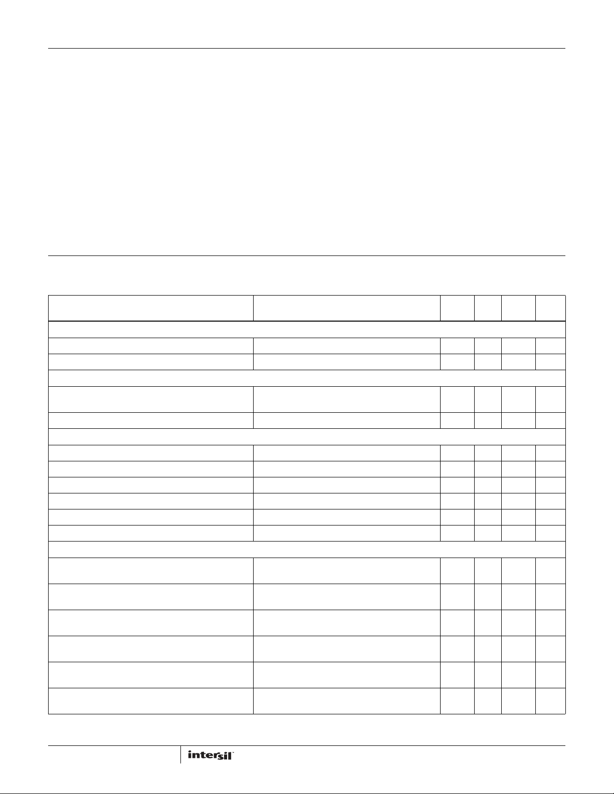
Absolute Maximum Ratings Thermal Information
VCC, VR_RDY, VR_RDYS. . . . . . . . . . . . . . . . . . . . . . . . . . . . . . . . . . . . . . . +6V
All Other Pins . . . . . . . . . . . . . . . . . . . . . . . . . . . . . . GND -0.3V to V
CC
+ 0.3V
Recommended Operating Conditions
Supply Voltage, VCC . . . . . . . . . . . . . . . . . . . . . . . . . . . . . . . . . . . . . +5V ±5%
Ambient Temperature
ISL6364CRZ . . . . . . . . . . . . . . . . . . . . . . . . . . . . . . . . . . . . . 0°C to +70°C
ISL6364IRZ . . . . . . . . . . . . . . . . . . . . . . . . . . . . . . . . . . . . . -40°C to +85°C
CAUTION: Do not operate at or near the maximum ratings listed for extended periods of time. Exposure to such conditions may adversely impact product
reliability and result in failures not covered by warranty.
NOTES:
4. θ
is measured in free air with the component mounted on a high effective thermal conductivity test board with “direct attach” features. See Tech
JA
Brief TB379.
5. For θ
, the “case temp” location is the center of the exposed metal pad on the package underside.
JC
Thermal Resistance (Notes 4, 5) θ
48 Ld 6x6 QFN Package . . . . . . . . . . . . . . . 27 1.5
Maximum Junction Temperature . . . . . . . . . . . . . . . . . . . . . . . . . . . .+150°C
Maximum Storage Temperature Range . . . . . . . . . . . . . .-65°C to +150°C
Pb-free reflow profile . . . . . . . . . . . . . . . . . . . . . . . . . . . . . . . . see link below
http://www.intersil.com/pbfree/Pb-FreeReflow.asp
(°C/W) θ
JA
JC
(°C/W)
Electrical Specifications Recommended Operating Conditions, V
operating temperature range.
PARAMETER
= 5V, Unless Other wise specified. Boldface limits apply over the
CC
TEST CONDITIONS
MIN
(Note 7) TYP
MAX
(Note 7) UNITS
VOLTAGE REGULATOR (VR) ADDRESS
Multiple-Phase Voltage Regulator (VR0) ADDRESS 0 EVN C
Single-Phase Voltage Regulator (VR1) ADDRESS 1 ODD 7
VCC SUPPLY CURRENT
Nominal Supply VCC = 5VDC; EN_PWR = 5VDC; RT = 125kΩ,
ISEN1-4 = 80µA, ISL6364, 400kHz
Shutdown Supply VCC = 5VDC; EN_PWR = 0VDC; R
= 125kΩ 14 21 27.5 mA
T
21 28 33.5 mA
POWER-ON RESET AND ENABLE
VCC Rising POR Threshold 4.30 4.40 4.50 V
VCC Falling POR Threshold 3.75 3.90 4.00 V
EN_PWR_FT Rising Threshold 0.830 0.850 0.870 V
EN_PWR_FT Falling Threshold 0.730 0.750 0.770 V
EN_VTT Rising Threshold 0.830 0.850 0.870 V
EN_VTT Falling Threshold 0.730 0.750 0.770 V
REFERENCE VOLTAGE AND DAC
System Accuracy of ISL6364CRZ
(VID = 1V to 2.155V,
System Accuracy of ISL6364CRZ
(VID = 0.8V to 1V,
System Accuracy of ISL6364CRZ
(VID = 0.25V to 0.8V,
System Accuracy of ISL6364IRZ
(VID = 1V to 2.155V,
System Accuracy of ISL6364IRZ
(VID = 0.8V to 1V,
System Accuracy of ISL6364IRZ
(VID = 0.25V to 0.8V,
TJ = 0°C to +70°C)
TJ = 0°C to +70°C)
TJ = 0°C to +70°C)
TJ = -40°C to +85°C)
TJ = -40°C to +85°C)
TJ = -40°C to +85°C)
(Note 6, Closed-Loop)
(Note 6, Closed-Loop)
(Note 6, Closed-Loop)
(Note 6, Closed-Loop)
(Note 6, Closed-Loop)
(Note 6, Closed-Loop)
-0.5 - 0.5 %VID
-5 - 5 mV
-8 - 8 mV
-0.6 - 0.6 %VID
-6 - 6 mV
-9 - 9 mV
8
FN6861.0
December 22, 2010
Page 9
ISL6364
Electrical Specifications Recommended Operating Conditions, V
operating temperature range.
(Continued)
PARAMETER
= 5V, Unless Other wise specified. Boldface limits apply over the
CC
TEST CONDITIONS
MIN
(Note 7) TYP
MAX
(Note 7) UNITS
OSCILLATORS
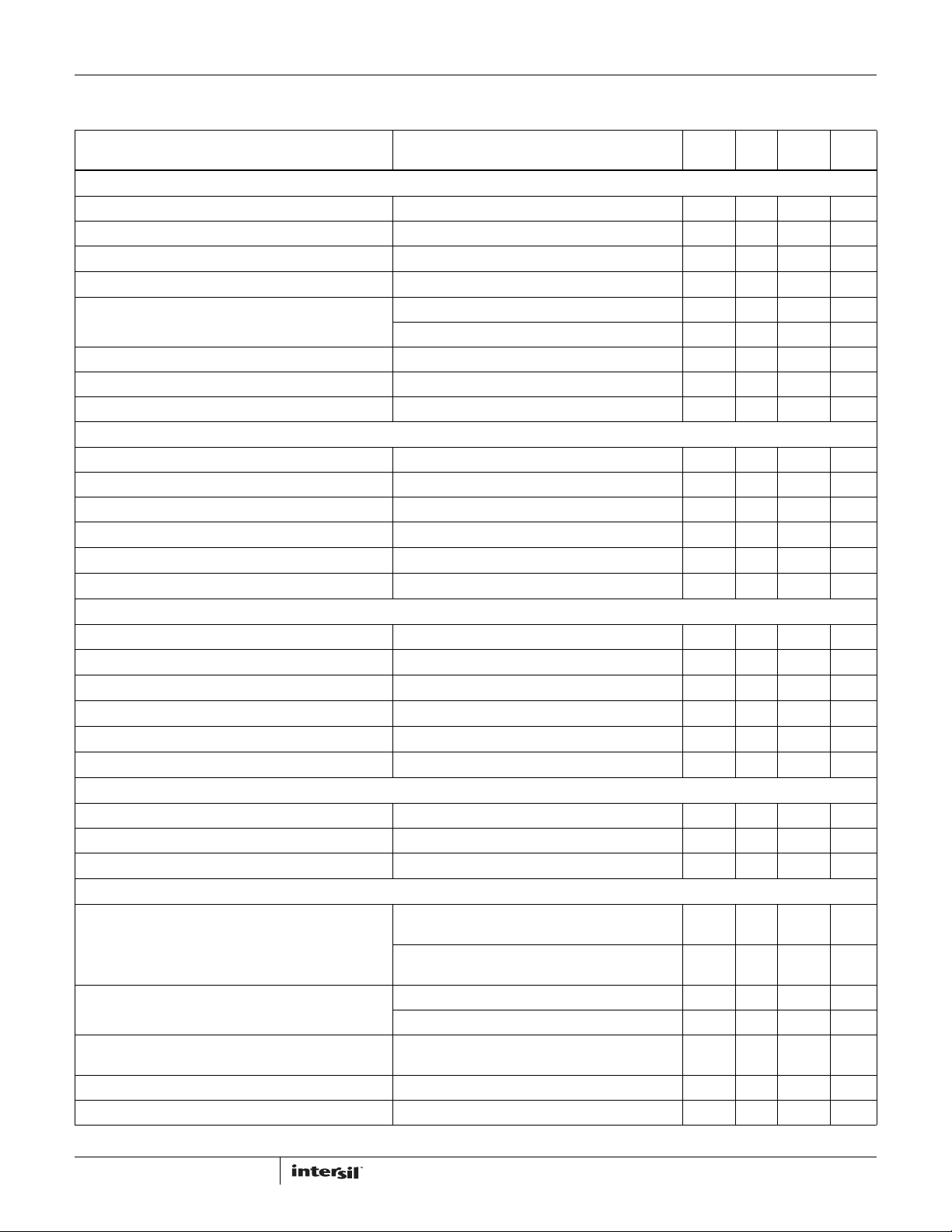
Accuracy of VR0 Switching Frequency Setting RFS = 125kΩ 360 400 440 kHz
Accuracy of VR1 Switching Frequency Setting R
Maximum Switching Frequency
Minimum Switching Frequency
Soft-start Ramp Rate for VR0
Soft-start Ramp Rate for VR1 2.5 2.8 3.2 mV/µs
Maximum Duty Cycle Per PWM for VR0 400kHz, V
Maximum Duty Cycle for VR1 400kHz 69 83 96 %
= 125kΩ 360 400 440 kHz
FSS
1.0 --MHz
--0.08 MHz
FDVID = 10mV/µs 2.5 2.8 3.2 mV/µs
FDVID = 20mV/µs 5.0 5.55 6.2 mV/µs
<1.8V 95 97 99 %
RAMP
PWM GENERATOR (Note 7)
Sawtooth Amplitude for VR0 R
Sawtooth Amplitude for VR0 R
Sawtooth Amplitude for VR0
Maximum Adjustable Ramp for VR0
Minimum Adjustable Ramp for VR0
Sawtooth Amplitude for VR1
RAMP_ADJ
RAMP_ADJ
R
RAMP_ADJ
Applicable to VR0 Only
Applicable to VR0 Only
Applicable to VR1 Only
= Open, all Switching Frequency -1- V
= 2.4 MΩ to 12V, 500kHz -0.5- V
= 1.2 MΩ to 12V, 500kHz -1- V
-3- V
-0.3- V
2.0 V
ERROR AMPLIFIER
Open-Loop Gain RL = 10kΩ to ground - 96 - dB
Open-Loop Bandwidth
Slew Rate
Maximum Output Voltage
Output High Voltage @ 2mA
Output Low Voltage @ 2mA
No Load
2mA Load
2mA Load
-80-MHz
-25-V/µs
4.1 4.4 4.6 V
3.8 4.1 4.6 V
0.85 0.96 1.2 V
PWM OUTPUT (PWM[4:1] and PWMS)
Sink Impedance PWM = Low with 1mA Load - 170 - Ω
Source Impedance PWM = High, Forced to 3.7V - 150 - Ω
PWM PSI2/3/Decay Mid-Level
0.4mA Load
38 40 44 %VCC
CURRENT SENSE AND OVERCURRENT PROTECTION
Sensed Current Tolerance of VR0 ISEN1-4= 40µA;
Sensed Current Tolerance of VR1 ISENS= 40µA; R
VR0 Average Overcurrent Trip Level at Normal CCM PWM
Mode
VR0 Average Overcurrent Trip Level at PSI1/2/3 Mode N = 4 Drop to 1-Phase - 99 - µA
VR0 Average Overcurrent Trip Level at PSI1 Mode N = 4 Drop to 2-Phase - 100 - µA
CS Offset and Mirror Error Included, R
ISEN1-4 = 80µA;
CS Offset and Mirror Error Included, R
= 100Ω; 33 37 41 µA
ISENS
ISENS = 80µA; R
CS Offset and Mirror Error Included, R
= 100Ω 69.5 75 81 µA
ISENS
= 12.8kΩ
SET
= 12.8kΩ
SET
= 12.8kΩ - 100 - µA
SET
36.5 40.7 44 µA
75.5 80.7 85.5 µA
9
FN6861.0
December 22, 2010
Page 10
ISL6364
Electrical Specifications Recommended Operating Conditions, V
operating temperature range.
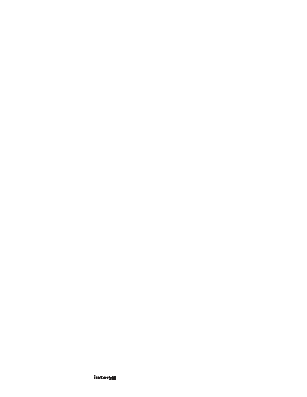
VR0 Peak Current Limit for Individual Channel - 140 - µA
VR1 Average Overcurrent Trip Level CS Offset and Mirror Error Included, R
IMON, IMOS Clamped and OCP Trip Level 1.085 1.12 1.14 V
IMON, IMONS IMAX TRIP POINT (FF) Higher than this will be “FF” 875 880 887 mV
(Continued)
PARAMETER
= 5V, Unless Other wise specified. Boldface limits apply over the
CC
TEST CONDITIONS
MIN
(Note 7) TYP
= 200Ω - 100 - µA
ISENS
MAX
(Note 7) UNITS
THERMAL MONITORING
VR_HOT# Pull-down Impedance 8.4 9.2 13 Ω
Thermal Trip (Programmable via TMAX) TMAX = +100°C, see Table 7 - 39.12 - %
VR_HOT# and Thermal Alert# Hysteresis -3-
Leakage Current of VR_HOT# With external pull-up resistor connected to VCC - - 1 µA
VR READY AND PROTECTION MONITORS
Leakage Current of VR_RDY, VR_RDYS With pull-up resistor externally connected to VCC - - 1 µA
VR READY Low Voltage 4mA Load - - 0.3 V
Overvoltage Protection Threshold Prior to the End of Soft Start 2.3 V
After the End of Soft Start, the voltage above VID 160 179 200 mV
Overvoltage Protection Reset Hysteresis 98 107 117 mV
SVID BUS
ALERT# Pull-down Impedance -1113 Ω
SVDATA -1113 Ω
SVCLK Maximum Speed - 26.5 - MHz
SVCLK Minimum Speed - 13.0 - MHz
NOTES:
6. These parts are designed and adjusted for accuracy with all errors in the voltage loop included.
7. Compliance to datasheet limits is assured by one or more methods: production test, characterization and/or design.
0
C
10
FN6861.0
December 22, 2010
Page 11

ISL6364
Functional Pin Descriptions
Note: VR0 is the multi-phase voltage regulator. VR1 is the singlephase voltage regulator. Refer to Table 13 on page 35 and
Table 14 on page 39 for Design and Layout Consideration.
VCC - Supplies the power necessary to operate the chip. The
controller starts to operate when the voltage on this pin exceeds
the rising POR threshold and shuts down when the voltage on
this pin drops below the falling POR threshold. Connect this pin
directly to a +5V supply with a high quality ceramic capacitor.
GND - The bottom metal base of ISL6364 is the GND. Bias and
reference ground for the IC. It is also the return for all PWM
output drivers.
EN_PWR - This pin is a threshold-sensitive enable input.
Connecting the power train input supply to this through an
appropriate resistor divider provides a means to synchronize the
power sequencing of the controller and the MOSFET driver ICs.
When EN_PWR is driven above 0.85V, the ISL6364 is actively
depending on status of the EN_VTT, the internal POR, and
pending fault states. Driving EN_PWR below 0.75V will clear all
fault states and prepare the ISL6364 to soft-start when reenabled.
EN_VTT - This pin is a threshold-sensitive enable input. It’s
typically connected to the output of the VTT voltage regulator in
the computer mother board. When this pin is driven above 0.85V,
the ISL6364 is actively depending on status of the EN_PWR, the
internal POR, and pending fault states. Driving this below 0.75V
will clear all fault states and prepare the ISL6364 to soft-start
when re-enabled.
VSEN - This pin monitors the regulator VR0 output for overvoltage protection. Connect this pin to the positive rail remote
sensing point of the microprocessor or load. This pin tracks with
the FB pin. If a resistive divider is placed on the FB pin, a resistive
divider with the same ratio should also be on the VSEN pin. Tie it
to GND if not used.
RGND - This pin compensates the offset between the remote
ground of the VR0 load and the local ground of this device.
Connect this pin to the negative rail remote sensing point of the
microprocessor or load. Tie it to GND if not used.
COMP and FB - COMP and FB are the output and inverting input
of the precision error amplifier, respectively. A type III loop
compensation network should be connected to these pins, while
the FB’s R-C network should connect to the positive rail remote
sensing point of the microprocessor or load. Combined with
RGND, the potential difference between remote and local rails is
completely compensated and it improves regulation accuracy. A
properly chosen resistor between FB and remote sensing point
can set the load line (droop, if enabled), because the sensed
current will flow out of FB pin. The droop scale factor is set by the
ratio of the effective ISEN resistors (set by RSET) and the inductor
DCR or the dedicated current sense resistor. COMP is tied back to
FB through an external R-C network to compensate the regulator.
An RC from the FB pin to ground will be needed if the output is
lagging from the DAC, typically for applications with too many
output capacitors and droop enabled.
VR_RDY - VR_RDY indicates that soft-start has completed and
this VR0 output remains in normal operation. It is an open-drain
logic output. When OCP or OVP occurs in VR0, VR_RDY will be
pulled to low.
TM - TM is an input pin for the VR0 temperature measurement.
Connect this pin through an NTC thermistor to GND and a resistor
to VCC of the controller. The voltage at this pin is inversely
proportional to the VR temperature. The device monitors the VR
temperature based on the voltage at the TM pin. Combining with
“TCOMP” setting, VR0’s sensed current is thermally compensated.
The VR_HOT# asserts low if the sensed temperature at this pin is
higher than the maximum desired temperature, “TMAX”. The NTC
should be placed close to the current sensing element, the output
inductor or dedicated sense resistor on Phase 1 of VR0. A
decoupling capacitor (0.1µF) is typically needed to be in close
proximity to the controller. If not used, connect this pin to TMS or
1MΩ/2MΩ resistor divider, but DON’T tie it to VCC or GND.
VR_HOT# - VR_HOT# is used as an indication of high VR
temperature. It is an open-drain logic output. It will be open if the
measured VR temperature is less than a certain level, and pulled
low when the measured VR temperature reaches a certain level.
PWM[4:1] - Pulse width modulation outputs of VR0. Connect
these pins to the PWM input pins of the Intersil driver IC. The
number of active channels is determined by the state of
PWM[4:2]. Tie PWM(N+1) to VCC to configure for N-phase
operation. PWM firing order is sequential from 1 to N with N
being the number of active phases. If PWM1 is tied high, the
respective address is released for use, i.e, the VR0 is disabled
and does not respond to the SVID commands. IMON, VSEN, FB,
ISEN[4:1]-, and RGND must be grounded to remove OCP and OVP
faults of VR0, while TM can be tied to TMS, or 1/2 ratio resistor
divider. In addition, must connect FS_DRP to 1MΩ from GND or
VCC. See Table page 15 on and Table 13 on page 35 for details.
PWMS - Pulse width modulation output of VR1. Connect this pin
to the PWM input pin of the Intersil driver IC. Tie this pin to VCC to
disable this PWM channel, while the respective address is
released for use, i.e., the VR1 is disabled and does not respond to
the SVID commands. IMONS, VSENS, FBS, ISENS-, and RGNDS
must be grounded to remove OCP and OVP faults of VR1, while
TMS can be tied to TM, or 1/2 ratio resistor divider. In addition,
must connect FSS_DRPS to 1MΩ from GND or VCC for proper
SVID address. See Table 13 for details.
ISEN[4:1]+, ISEN[4:1]- - The ISEN+ and ISEN- pins are current
sense inputs to individual differential amplifiers of VR0. The
sensed current is used for channel current balancing, overcurrent
protection, and droop regulation. Inactive channels should have
their respective current sense inputs, ISEN[4:#]- grounded, and
ISEN[4:#]+ open. For example, ground ISEN[4:3]- and open
ISEN[4:3]+ for 2-phase operation. DON’T ground ISEN[4:1]+. For
DCR sensing, connect each ISEN- pin to the node between the RC
sense elements. Tie the ISEN+ pin to the other end of the sense
capacitor (typically output rail). The voltage across the sense
capacitor is proportional to the inductor current. Therefore, the
sensed current is proportional to the inductor current and scaled
by the DCR of the inductor and R
ISEN[4:1]- grounded and ISEN[4:1]+ open.
RSET - A resistor connected from this pin to ground sets the
current gain of the current sensing amplifier for VR0. The RSET
resistor value can be from 3.84kΩ
required R
resistor value. Therefore, the current sense gain
ISEN
. When VR0 is disabled, have
SET
to 115.2kΩ and is 64x of the
11
FN6861.0
December 22, 2010
Page 12

ISL6364
resistor value can be effectively set at 60Ω to 1.8kΩ. When VR0
is disabled (PWM1 = VCC), connect 1MΩ from this pin to GND.
ISENS+, ISENS- - The ISENS+ and ISENS- pins are current
sense inputs to the differential amplifier of VR1. The sensed
current is used for overcurrent protection and droop regulation.
For DCR sensing, connect each ISENS- pin to the node between
the RC sense elements. Tie the ISENS+ pin to the other end of
the sense capacitor through a resistor, R
. The voltage
ISENS
across the sense capacitor is proportional to the inductor current.
Therefore, the sense current is proportional to the inductor
current and scaled by the DCR of the inductor and R
ISENS
. When
VR1 is disabled, have ISENS- grounded and ISENS+ open.
IMON - IMON is the output pin of sensed, thermally compensated
(if internal thermal compensation is used) average current of VR0.
The voltage at the IMON pin is proportional to the load current and
the resistor value, and internally clamped to 1.12V. If the clamped
voltage is triggered, it will initiate an overcurrent shutdown. By
choosing the proper value for the resistor at IMON pin, the
overcurrent trip level can be set to be lower than the fixed internal
overcurrent threshold. During the dynamic VID, the OCP function of
this pin is disabled to avoid false triggering. Tie it to GND if not
used. Does not need to refer to the remote ground for
VR12/IMPV7 applications.
FS_DRP - A resistor placed from this pin to GND/VCC will set the
switching frequency of VR0. The relationship between the value
of the resistor and the switching frequency will be approximated
by Equation 4 on page 16. This pin is also used to set the droop
option. The droop is disabled when the resistor is pulled to VCC
and enabled when the resistor is pulled to ground. When VR0 is
disabled (PWM1 = VCC), connect 1MΩ from this pin to GND.
HFCOMP - Connect a resistor with a similar value of the feedback
impedance to the VR0 output to compensate the level-shifted
output voltage during high-frequency load transient events.
Connecting more than 2x of feedback impedance to this pin or
keeping it open virtually disables this feature.
PSICOMP - Connect an RC to the type III compensation capacitor
of the VR0 output voltage. This improves loop gain and load
transient response in PSI1/2/3/Decay mode. An open pin will
disable this feature.
SICI - When this pin is pulled to ground, it sets for standard-inductor
(SI) operation; when this pin is pulled to VCC, it sets coupled-inductor
(CI) operation. The phase dropping operation options for PSI1/2/3
mode are summarized in Table 3 on page 16. The ISL6364A will
re-name this pin as “IAUTO” for auto phase shedding operation,
while the standard and coupled-inductor programmable option is
still valid on this pin.
VSENS, RGNDS, FBS, COMPS, VR_RDYS, IMONS, FSS_DRPS,
HFCOMPS - These pins are for VR1 regulator and have the same
function as VSEN, RGND, FB, COMP, VR_RDY, IMON, FS_DRP, and
HFCOMP, respectively. However, HFCOMPS has multiplexed the
DVCS function, while the FSS_DRPS does have additional
programming feature as described in the following.
pin or keeping it open virtually disables this feature. If the droop
option of VR1 is disabled, then this pin becomes DVCS. A series
resistor and capacitor can be connected from this pin to the FBS
pin to compensate and smooth dynamic VID transitions for VR1
output.
FSS_DRPS - A resistor placed from this pin to ground/VCC will set
the switching frequency of VR1. The relationship between the
value of the resistor and the switching frequency will be
approximated by Equation 4 on page 16. This pin is also used to
set the droop option. The droop is disabled when the resistor is
pulled to VCC and enabled when the resistor is pulled to ground.
When VR1 is disabled (PWMS = VCC), connect 1MΩ from this pin
to GND for ADDR: 0, 2, 4, and 6; to VCC for ADDR: 8, A, and C.
TMS - This is an input pin for the temperature monitoring. Connect
this pin through an NTC thermistor to GND and a resistor to VCC of
the controller. The voltage at this pin is inversely proportional to
the VR temperature. The thermal information can be used for VR1
thermal compensation. If TCOMPS is set at “OFF” bit, the
integrated thermal compensation is disabled; otherwise, the
thermal information is used for VR1 thermal compensation with
“TCOMPS” data. Combined with TM pin, the thermal information at
TMS pin will also be used to trigger VR_HOT#. The NTC should be
placed close to the current sensing element, the output inductor or
dedicated sense resistor of VR1. A decoupling capacitor (0.1µF) is
typically needed to be in close proximity to the controller. If not
used, connect this pin to TM or 1MΩ/2MΩ resistor divider, but
DON’T tie it to VCC or GND.
SVCLK - An input pin for a synchronous clock signal of SerialVID
bus from CPU.
SVDATA - An input pin for transferring open-drain data signals
between CPU and VR controller.
SVALERT# - An output pin for transferring the active low signal
driven asynchronously from the VR controller to CPU.
RAMP_ADJ - An input pin to set the slope of Sawtooth for VR0.
The slope of the Sawtooth is proportional to the current, sampled
by the an active pull-down device, into this pin. When the resistor
is connected to the input voltage of the VR0, the slope will be
proportional to the input voltage, achieving voltage feed-forward
compensation. For a 12V supply (V
) and 2.4MΩ pull-up (~ 5µA),
IN
it sets a nominal 0.25V/µs up-ramp slope at 500kHz switching
frequency, corresponding to 0.5V peak-to-peak up ramp. The
maximum peak-to-peak up ramp should be limited to 3V,
corresponding a pull-down current of 30µA at 500kHz, i.e., the
pull-up impedance should be higher than V
/30µA at 500kHz.
IN
See Equation 3 on page 15 for the up ramp amplitude
calculation. When this pin is floating, the up ramp amplitude sets
to 1V regardless of the switching frequency and the feedforward
function is disabled.
ADDR_IMAXS_TMAX, BTS_DES_TCOMPS, BT_FDVID_TCOMP,
NSPI_DE_IMAX - These are four register pins to program system
parameters. The meaning of each is described in the following.
See Table 9 on page 33 for the summary.
HFCOMPS/DVCS - Connect a resistor with a similar value of the
feedback impedance to the VR1 output to compensate the levelshifted output voltage during high-frequency load transient
events. Connecting more than 2x of feedback impedance to this
12
ADDR_IMAXS_TMAX (0C):
ADDR - An input pin to set the address offset register of VR0 (0,
2, 4, 6, 8, A, C) and VR1 (1, 3, 5, 7). E/F is an ALL call address
and is not used.
FN6861.0
December 22, 2010
Page 13

ISL6364
IMAXS - An input pin to set the maximum current, I
register of the VR1. It can be programed to 20A, 25A, 30A, and
35A when the droop is enabled (R
represents the maximum allowed load current for VR1 and
corresponds to a 900mV (typically set) at IMONS. When VR1
droop is disabled (R
programed to15A, 20A, 25A, and 30A.
TMAX - An input pin to set the maximum temperature register
(TMAX) of the VR0 and VR1 and the thermal trip point of
VR_HOT#. It covers +90°C to +120°C with 5°C/step. The
register represents the maximum allowed temperature of VR0
and VR1, and programs the over-temperature trip point at
VR_HOT#. The typical application should use +100°C or lower
since the NTC thermistor temperature represents the PCB, not
the hottest component on the board. In addition, the NTC
thermistor typically picks up a temperature lower than the PCB
due to the thermal impedance between PCB and NTC.
BTS_DES_TCOMPS (0D):
BTS - An input pin to set the start-up boot voltage register of VR1.
It has four levels: 0, 0.9V, 1.0, and 1.1V for graphic rails with
droop enabled (R
(R
FSS_DRPS
0.925V, 1.05V for VCCIO and System Agent rails.
DES - An input pin to set the diode emulation (DE) operation
register of VR1 at PSI2, PSI3, and Decay modes. At PSI1 mode,
the VR1 always operates in CCM mode. When the diode
emulation is disabled, the output will decay at the rate of setVID
Slow; however, the SVID bus is still be acknowledged of execution
of the command.
TCOMPS - An input pin to set the mis-matching temperature
(+13°C to +43°C) between the actual sensed inductor and the NTC
thermistor at TMS pin. The voltage sensed on the TMS pin is utilized
as the temperature input to adjust the droop current and the
overcurrent protection limit to effectively compensate for the
temperature coefficient of the current sense element of VR1. To
implement the integrated temperature compensation, select a
proper temperature offset “TCOMP,” other than the “OFF” value,
which is to disable the integrated temperature compensation
function.
BT_FDVID_TCOMP (0E):
BT - An input pin to set the start-up boot voltage register of VR0.
It has four levels: 0V, 0.9V, 1.0V, and 1.1V for core applications
with droop enabled (R
disabled (R
1.2V, 1.35V, and 1.5V for memory applications.
FDVID - An input pin to set the slew rate of fast Dynamic VID. It
has choices of 10mV/µs and 20mV/µs. This will only apply to
VR0, not VR1.
TCOMP - An input to set the mis-matching temperature (+13°C to
+43°C) between the actual sensed inductor of VR0 regulator and
the NTC thermistor at the TM pin. The voltage sensed on the TM pin
is utilized as the temperature input to adjust the droop current and
the overcurrent protection limit to effectively compensate for the
temperature coefficient of the current sense element of VR0. To
implement the integrated temperature compensation, select a
proper temperature offset “TCOMP,” other than the “OFF” value,
= VCC), the boot levels will be changed to 0, 0.85V,
FS_DRP
FSS_DRPS
FSS_DRPS
FS_DRP
= VCC), the boot levels will be changed to 0V,
FSS_DRPS
= VCC), the I
= GND). When the droop is disabled
= GND). When the droop is
= GND). This register
can be
CCMAX
CCMAX
,
which is to disable the integrated temperature compensation
function.
NSPI_DE_IMAX (0F):
NPSI - An input pin to set the number of phases dropping at low
power mode. See Table 3 on page 16 for more details.
DE - An input pin to set the diode emulation (DE) operation
register of VR0 at PSI2, PSI3, and Decay modes. At PSI1 mode,
the VR0 always operates in CCM mode. When the diode
emulation is disabled, the output will decay at the rate of setVID
Slow; however, the SVID bus is still be acknowledged of execution
of the command.
IMAX - An input pin to set the maximum current, I
of the VR0 voltage regulator. It has a range of 15A to 165A with
5A/step.This register represents the maximum allowed load
current for VR0 and corresponds to a 900mV (typically set) at
IMON.
CCMAX
, register
Operation
The ISL6364 is a dual PWM controller; its 4-phase PWMs control
microprocessor core or memory voltage regulator, while its singlephase PWM controls the peripheral voltage regulator such
graphics rail, system agent, or processor I/O. The ISL6364 is
designed to be compliant to Intel VR12/IMVP7 specifications with
SerialVID Features. The system parameters and SVID required
registers are programmable with four dedicated pins. It greatly
simplifies the system design for various platforms and lowers
inventory complexity and cost by using a single device.
In addition, this controller is compatible, except for forced phase
dropping via PWM lines, with phase doublers (ISL6611A and
ISL6617), which can double or quadruple the phase count. For
instance, the multi-phase PWM can realize a beyond 4-phase and
up to 16-phase count system, and the single-phase PWM can be
scaled up to 2 or 4 phases. The higher phase count system can
improve thermal distribution and power conversion efficiency at
heavy load.
Multiphase Power Conversion
Microprocessor load current profiles have changed to the point
that the advantages of multiphase power conversion are
impossible to ignore. The technical challenges associated with
producing a single-phase converter (which are both cost-effective
and thermally viable), have forced a change to the cost-saving
approach of multiphase. The ISL6364 controller helps reduce the
complexity of implementation by integrating vital functions and
requiring minimal output components. The typical application
circuits diagrams on page 5 and page 6 provide the top level
views of multiphase power conversion using the ISL6364
controller.
Interleaving
The switching of each channel in a multiphase converter is timed
to be symmetrically out-of-phase with each of the other channels.
In a 3-phase converter, each channel switches 1/3 cycle after the
previous channel and 1/3 cycle before the following channel. As
a result, the 3-phase converter has a combined ripple frequency
three times greater than the ripple frequency of any one phase,
13
FN6861.0
December 22, 2010
Page 14
ISL6364
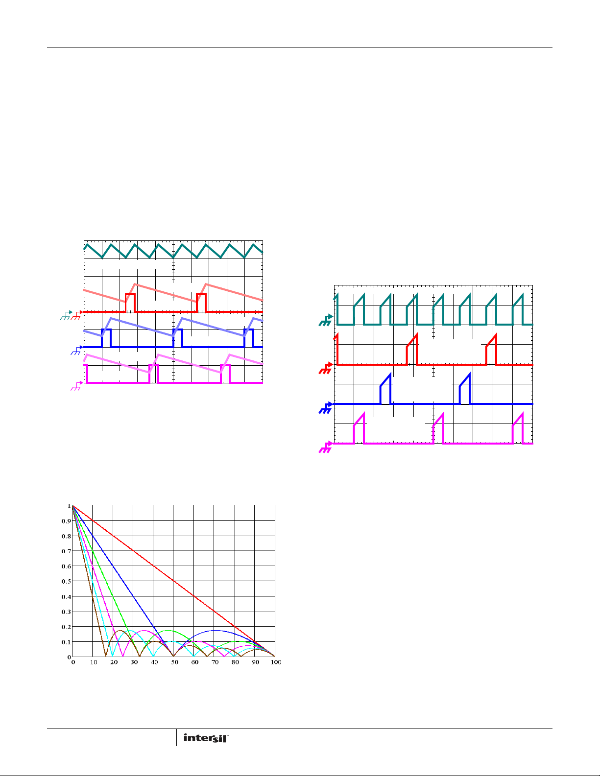
as illustrated in Figure 1. The three channel currents (IL1, IL2,
and IL3) combine to form the AC ripple current and the DC load
current. The ripple component has three times the ripple
frequency of each individual channel current. Each PWM pulse is
terminated 1/3 of a cycle after the PWM pulse of the previous
phase. The DC components of the inductor currents combine to
feed the load.
To understand the reduction of ripple current amplitude in the
multiphase circuit, examine Equation 1, which represents an
individual channel’s peak-to-peak inductor current.
VINV
----------------------------------------------------------=
L F
–()V
I
PP
In Equation 1, V
respectively, L is the single-channel inductor value, and F
⋅
OUT
SW
IN
⋅
V⋅
IN
and V
OUT
are the input and output voltages
OUT
(EQ. 1)
SW
is
the switching frequency.
IL1 + IL2 + IL3, 7A/DIV
IL1, 7A/DIV
PWM1, 5V/DIV
IL2, 7A/DIV
PWM2, 5V/DIV
IL3, 7A/DIV
Output voltage ripple is a function of capacitance, capacitor
equivalent series resistance (ESR), and the summed inductor
ripple current. Increased ripple frequency and lower ripple
amplitude mean that the designer can use less per-channel
inductance and few or less costly output capacitors for any
performance specification.
V
OUT
I
------------------
=
CPP,
for
LFSW⋅
K
K
RCM
ND⋅ m– 1+()mND⋅()–()⋅
--------------------------------------------------------------------------- -
=
RCM
m1– ND⋅ m≤≤
mROUNDUPND⋅ 0,()=
ND⋅
(EQ. 2)
Another benefit of interleaving is to reduce input ripple current.
Input capacitance is determined in part by the maximum input
ripple current. Multiphase topologies can improve overall system
cost and size by lowering input ripple current and allowing the
designer to reduce the cost of input capacitors. The example in
Figure 3 illustrates input currents from a three-phase converter
combining to reduce the total input ripple current.
INPUT-CAPACITOR CURRENT, 10A/DIV
CHANNEL 1
INPUT CURRENT
10A/DIV
PWM3, 5V/DIV
1µs/DIV
FIGURE 1. PWM AND INDUCTOR-CURRENT WAVEFORMS FOR
3-PHASE CONVERTER
In the case of multiphase converters, the capacitor current is the
sum of the ripple currents from each of the individual channels.
Compare Equation 1 to the expression for the peak-to-peak
current after the summation of N symmetrically phase-shifted
inductor currents in Equation 2, the peak-to-peak overall ripple
current (I
) decreases with the increase in the number of
C,PP
channels, as shown in Figure 2.
RCM
N=1
2
3
4
RIPPLE CURRENT MULTIPLIER, K
FIGURE 2. RIPPLE CURRENT MULTIPLIER vs DUTY CYCLE
5
6
DUTY CYCLE (V
OUT/VIN
)
CHANNEL 2
INPUT CURRENT
10A/DIV
CHANNEL 3
INPUT CURRENT
10A/DIV
1µs/DI
FIGURE 3. CHANNEL INPUT CURRENTS AND INPUT-CAPACITOR
RMS CURRENT FOR 3-PHASE CONVERTER
The converter depicted in Figure 3 delivers 36A to a 1.5V load from
a 12V input. The RMS input capacitor current is 5.9A. Compare this
to a single-phase converter also stepping down 12V to 1.5V at 36A.
The single-phase converter has 11.9A
input capacitor current.
RMS
The single-phase converter must use an input capacitor bank with
twice the RMS current capacity as the equivalent three-phase
converter.
Figures 29, 30 and 31, as described in “Input Capacitor
Selection” on page 38 , can be used to determine the input
capacitor RMS current based on load current, duty cycle, and the
number of channels. They are provided as aids in determining
the optimal input capacitor solution. Figure 32 shows the single
phase input-capacitor RMS current for comparison.
PWM Modulation Scheme
The ISL6364 adopts Intersil's proprietary Enhanced Active Pulse
Positioning (EAPP) modulation scheme to improve transient
performance. The EAPP is a unique dual-edge PWM modulation
scheme with both PWM leading and trailing edges being
14
FN6861.0
December 22, 2010
Page 15
ISL6364
independently moved to give the best response to transient
loads. The EAPP has an inherited function, similar to Intersil's
proprietary Adaptive Phase Alignment (APA) technique, which
turns on all phases together in order to further improve the
transient response when there are sufficiently large load step
currents. The EAPP is a variable frequency but linear control over
the transient events such that it can evenly distribute the pulses
among all phases to achieve a very good current balance and
eliminate the beat frequency oscillation over wide frequency
range of load transients.
To further improve the line and load transient responses, the
multi-phase PWM features feedforward function to change the
up ramp with the input line to maintain a constant overall loop
gain over a wide range input voltage. The up ramp of the internal
Sawtooth is defined in Equation 3.
V
RAMP
51010V⋅⋅
----------------------------------------------
=
FSWR⋅
IN
RAMP_ADJ
(EQ. 3)
With EAPP control and feedforward function, the ISL6364 can
achieve excellent transient performance over wide frequency
range of load step, resulting in lower demand on the output
capacitors.
At DC load conditions, the PWM frequency is constant and set by
the external resistor between the FS pin and GND during normal
mode (PSI0) and low power mode (PSI1). However, when PSI2 or
PSI3 is asserted in ultra low power conditions and if the VR is
configured into diode emulation operation, the EAPP reduces the
switching frequency as the load decreases. Thus, the VR can
enter burst mode at extreme light load conditions and improve
power conversion efficiency significantly.
Under steady state conditions, the operation of the ISL6364
PWM modulator appears to be that of a conventional trailing
edge modulator. Conventional analysis and design methods can
therefore be used for steady state and small signal operation.
The single-phase PWM has a fix ramp of 2V peak to peak. Its
modulation gain does not change with the input line.
PWM and PSI# Operation
The timing of each channel is set by the number of active
channels. The default channel setting for the ISL6364 is four. The
switching cycle is defined as the time between PWM pulse
termination signals of each channel. The cycle time of the pulse
signal is the inverse of the switching frequency set by the resistor
between the FS pin and ground. The PWM signals command the
MOSFET driver to turn on/off the channel MOSFETs.
The ISL6364 can work in a 0 to 4-Phase configuration. Tie
PWM(N+1) to VCC to configure for N-phase operation. PWM firing
order is sequential from 1 to N with N being the number of active
phases, as summarized in Table 1. For 4-phase operation, the
channel firing sequence is 1-2-3-4, and they are evenly spaced
1/4 of a cycle. Connecting PWM4 to VCC configures 3-phase
operation, the channel firing order is 1-2-3 and the phase spacing
is 1/3 of a cycle. If PWM2 is connected to VCC, only Channel 1
operation is selected. If PWM1 is connected to VCC, the
multi-phase (VR0) operation is turned off; to ensure proper
operation of VR1, the VR0’s respective pins should be configured
as described in “Disabling Output” on page 35.
TABLE 1. PHASE NUMBER AND PWM FIRING SEQUENCE
PHASE SEQUENCE
N
4 1-2-3-4 - PWM1/3
3 1-2-3 PWM4 PWM1/2
2 1-2 PWM3 PWM1/2
1 1 PWM2 PWM1
0OFF PWM1 OFF
PSI# = PSI0
PWM# TIED
TO VCC
ACTIVE PHASE
PSI# = PSI1
The CPU can enter four distinct power states, as shown in Table 2.
The ISL6364 supports all states, but it treats PSI2 and PSI3 the
same. In addition, the setDecay mode will automatically enter PSI2
state while decaying the output voltage. However, prior to the end of
soft-start (i.e: VR_RDY goes high), the lower power mode
(PSI1/2/3/Decay) is NOT enabled.
TABLE 2. POWER STATE COMMAND FROM CPU
STATE DESCRIPTION
PSI0 High Power Mode, All Phases are running
PSI1 Low Power Mode
PSI2 Very Low Power Mode
PSI3 Ultra Low Power Mode, treated as PSI2
Decay Automatically entering PSI2 and Ramping down the output
voltage to a target voltage in Decay Mode
When the SVID bus sends PSI1/2/3 or setVID Decay command, it
indicates the low power mode operation of the processor. The
controller will start phase shedding the next switching pulse. The
controller allows to drop the number of active phases according to
the logic on Table 3 for high light load efficiency performance. The
“NPSI” register and SICI pin are to program the controller in
operation of non-coupled (SI), 2-phase coupled, or (N-x)-Phase
coupled inductors. Different cases yield different PWM output
behaviors on both dropped phase(s) and operational phase(s) as
PSI# is asserted and de-asserted. When CPU sends PSI0 command,
it will pull the controller back to normal CCM PWM operation to
sustain an immediate heavy transient load and high efficiency. Note
that “N-x” means N-x phase coupled and x phase(s) are uncoupled.
For 2-Phase coupled inductor (CI) operation, both coupled phases
should be 180° out of phase. In low power states
(PSI1/2/3/Decay), the opposite phase of the operational phase
will turn on its Low-side MOSFET to circulate inductor current to
minimize conduction loss when Phase 1 is high.
When PSI1 is asserted, the VR0 is in single-phase CCM operation
with PWM1, or 2-phase CCM operation with PWM1 and 2, or 3,
as shown in Table 1. The number of operational phases is
configured by “NPSI” register, shown in Table 3. In PSI2/3/Decay
state, only single phase is in DCM/CCM operation, which is
programmed by the “DE” register; the opposite PWM 2, or 3
(depending upon configured maximum phase number as in
Table 1) of the PWM1 however will pull low at PWM1 high in CI
applications.
15
FN6861.0
December 22, 2010
Page 16
ISL6364
TABLE 3. PHASE DROPPING CONFIGURATION AT PSI1 AND
PSI2/3/DECAY
PSI2/3
SICI NPSI CODE PSI1 Mode
0 0 SI1 SI, (N-1)-CI 1-Phase 1-Phase
0 1 SI2 SI, (N-2)-CI 2-Phase 1-Phase
1 0 CI1 2-Phase CI 1-Phase 1-Phase
1 1 CI2 2-Phase CI 2-Phase 1-Phase
NOTE: For 2-Phase CI option, the dropped coupled phase turns on LGATE
to circulate current when PWM1 is high.
The VR1 output can be disabled by pulling PWMS to VCC while the
respective address is released for use with a different VR controller.
For proper operation of VR0, the VR1’s respective pins should be
configured as described in “Disabling Output” on page 35.
While the controller is operational (VCC above POR, EN_VTT and
EN_PWR are both high, valid VID inputs), it can pull the PWM pins
to ~40% of VCC (~2V for 5V VCC bias) during various stages, such
as soft-start delay, phase shedding operation, or fault conditions
(OC or OV events). The matching driver's internal PWM resistor
divider can further raise the PWM potential, but not lower it
below the level set by the controller IC. The controller's PWM
outputs are directly compatible with Intersil drivers that require
5V PWM signal amplitudes. Drivers requiring 3.3V PWM signal
amplitudes are generally incompatible.
Diode Emulation Operation
To improve light efficiency, the ISL6364 can enter diode
emulation operation in PSI2/3 or Decay mode. Users however
should select Intersil VR12/IMVP7 compatible drivers: ISL6627
or ISL6625 for PSI# channel(s). The diode emulation should be
disabled if non-compatible power stages or drivers are used.
Switching Frequency
Both VR0 and VR1 can independently set switching frequency,
which is determined by the selection of the frequency-setting
resistor, R
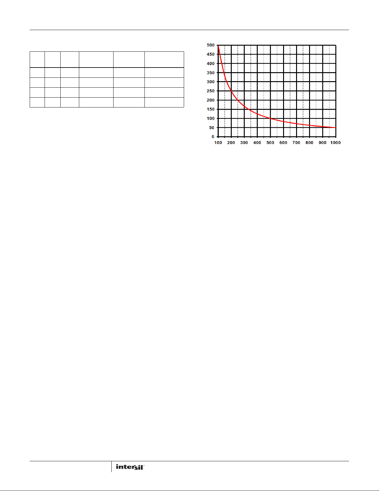
VCC. Equation 4 and Figure 4 are provided to assist in selecting
the correct resistor value.
R
T
where FSW is the switching frequency of each phase.
Independent frequency for VR0 and VR1 allows for cost,
efficiency, and performance optimization. Proximity between the
power trains of the two regulators imposed by the spaceconstrained layouts can lead to cross-coupling. To minimize the
effect of cross-coupling between regulators, select operating
frequencies at least 50kHz apart.
, which is connected from FS or FSS pin to GND or
T
10
5 10⋅
---------------------=
F
SW
& DECAY
(EQ. 4)
, kΩ)
T
FREQUENCY-SETTING RESISTOR VALUE (R
FIGURE 4. SWITCHING FREQUENCY vs RT
SWITCHING FREQUENCY (Hz)
Current Sensing
The ISL6364 senses current continuously for fast response. The
ISL6364 supports inductor DCR sensing, or resistive sensing
techniques. The associated channel current sense amplifier uses
the ISEN inputs to reproduce a signal proportional to the inductor
current, I
. The sense current, I
L
current. The sensed current is used for current balance, load-line
regulation, and overcurrent protection.
The internal circuitry, shown in Figures 5-6 and 9-10, represents
VR1’s channel or one channel of the VR0 output, respectively. For
VR0 output, the ISEN± circuitry is repeated for each channel, but
may not be active depending on the status of the PWM2, PWM3,
and PWM4 pins, as described in “PWM and PSI# Operation” on
page 15. The input bias current of the current sensing amplifier
is typically 60nA; less than 8.34k
offset) is preferred to minimized the offset error, i.e., a larger C
value as needed.
INDUCTOR DCR SENSING
An inductor’s winding is characteristic of a distributed resistance,
as measured by the DCR (Direct Current Resistance) parameter.
Consider the inductor DCR as a separate lumped quantity, as
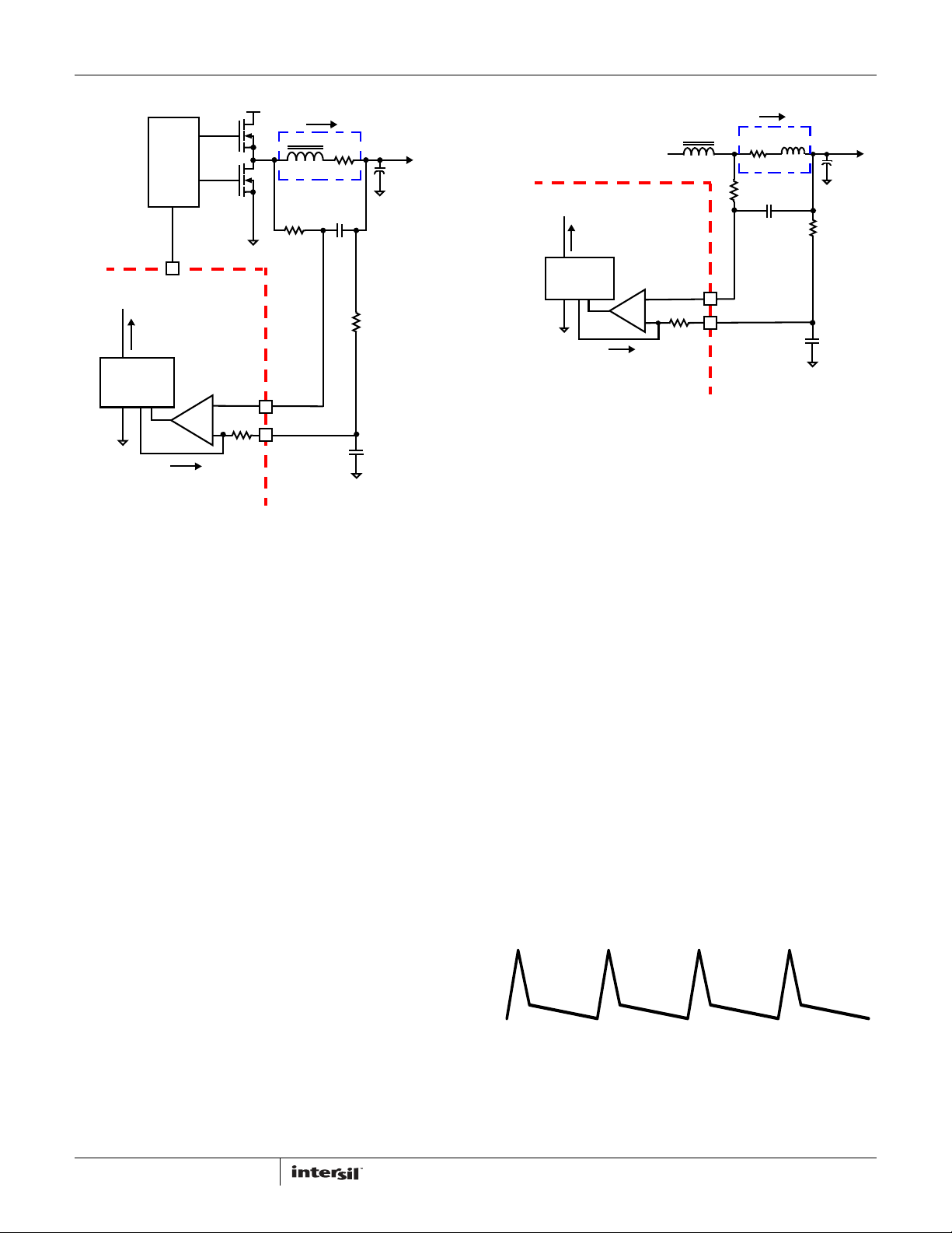
shown in Figure 5. The channel current I
inductor, will also pass through the DCR. Equation 5 shows the sdomain equivalent voltage across the inductor VL.
VLs() ILsL DCR+⋅()⋅=
A simple R-C network across the inductor extracts the DCR
voltage, as shown in Figure 5.
, is proportional to the inductor
SEN
Ω input impedance (0.5mV
, flowing through the
L
(EQ. 5)
16
FN6861.0
December 22, 2010
Page 17
ISL6364
V
ISL6364
In
CURRENT
SENSE
I
SEN
ISL6596
----------------------------------
I
=
L
10.5 R+
IN
PWMS
+
-
10.5
DCR
ISEN
L
INDUCTOR
R
ISENS-
ISENS+
ILs()
V
+
L
VC(s)
+
DCR
-
C
-
R
C
V
C
OUT
ISEN(n)
T
OUT
FIGURE 5. DCR SENSING CONFIGURATION FOR VR1
The voltage on the capacitor VC, can be shown to be proportional
to the channel current IL. See Equation 6.
L
⎛⎞
----------- -
VCs()
s
⋅ 1+
⎝⎠
DCR
-----------------------------------------------------------------
=
sRC 1+⋅()
DCR I
⋅()⋅
L
(EQ. 6)
If the R-C network components are selected such that the RC time
constant matches the inductor time constant (R*C = L/DCR), the
voltage across the capacitor VC is equal to the voltage drop across
the DCR, i.e., proportional to the channel current.
I
L
L
R
I
SEN
ISL6364
CURRENT
I
=
L
In
SENSE
R
SEN
----------------------------------
10.5 R+
ISEN
ESL
SEN
R
SENSE
-
V
+
R
R
ISENS-
+
10.5
-
ISENS+
VC(s)
+
-
C
C
R
ISEN(n)
C
T
V
OUT
OUT
FIGURE 6. SENSE RESISTOR IN SERIES WITH INDUCTOR FOR
VR1
A current sensing resistor has a distributed parasitic inductance,
known as ESL (equivalent series inductance, typically less than
1nH) parameter. Consider the ESL as a separate lumped
quantity, as shown in Figure 6. The channel current I
, flowing
L
through the inductor, will also pass through the ESL. Equation 8
shows the s-domain equivalent voltage across the resistor V
VRs() ILsESL R
+⋅()⋅=
SEN
.
R
(EQ. 8)
A simple R-C network across the current sense resistor extracts
the R
The voltage on the capacitor V
voltage, as shown in Figure 6.
SEN
, can be shown to be proportional
C
to the channel current IL. See Equation 9.
ESL
⎛⎞
------------- -
s
⋅ 1+
⎝⎠
R
SEN
-------------------------------------------------------------------- -
=
s()
V
C
sRC 1+⋅()
R
SENIL
⋅()⋅
(EQ. 9)
With the internal low-offset current amplifier, the capacitor
voltage V
Therefore, the current out of the ISENS+ pin, I
is replicated across the sense resistor R
C
SEN
.
ISEN
, is proportional
to the inductor current.
Because of the internal filter at the ISENS- pin, one capacitor, C
is needed to match the time delay between the ISENS- and
ISENS+ signals. Select the proper C
R
ISEN
and CT (R
x CT) close to 27ns.
ISEN
to keep the time constant of
T
Equation 7 shows that the ratio of the channel current to the
sensed current, I
, is driven by the value of the sense resistor
SEN
and the DCR of the inductor.
DCR
I
SENIL
---------------
⋅=
R
ISEN
(EQ. 7)
RESISTIVE SENSING
For more accurate current sensing, a dedicated current-sense
resistor R
current sense element (see Figure 6). This technique however
reduces overall converter efficiency due to the additional power loss
on the current sense element R
in series with each output inductor can serve as the
SENSE
.
SENSE
17
If the R-C network components are selected such that the RC
time constant matches the ESL-R
(R*C = ESL/R
the voltage drop across the R
current. As an example, a typical 1mΩ sense resistor can use
,
T
R = 348 and C = 820pF for the matching. Figures 7 and 8 show
), the voltage across the capacitor VC is equal to
SEN
SEN
time constant
SEN
, i.e., proportional to the channel
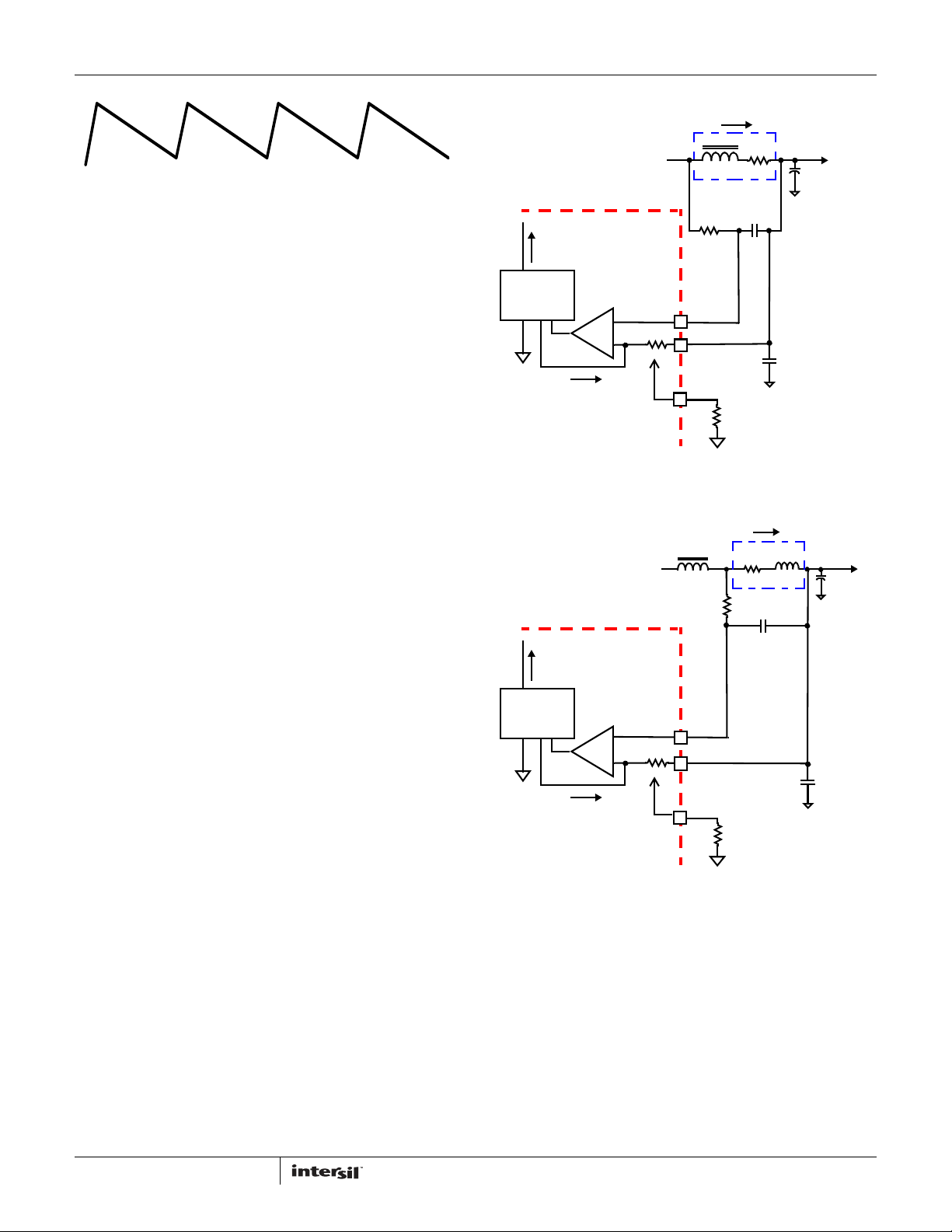
the sensed waveforms without and with matching RC when using
resistive sense.
Because of the internal filter at the ISENS- pin, one capacitor, C
is needed to match the time delay between the ISENS- and
ISENS+ signals. Select the proper C
R
and CT (R
ISEN
x CT) close to 27ns.
ISEN
FIGURE 7. VOLTAGE ACROSS R WITHOUT RC
to keep the time constant of
T
December 22, 2010
FN6861.0
,
T
Page 18
ISL6364
FIGURE 8. VOLTAGE ACROSS C WITH MATCHING RC
Equation 10 shows that the ratio of the channel current to the
sensed current, I
and the R
I
SENIL
ISEN
⋅=
---------------
R
Figures 5 and 7 configurations apply for VR1 output, while the
R
should include the internal metal impedance of 10.5Ω for
ISEN
accurate current sense.
For VR0 output, the R
while its value is determined by the R
resistor value can be from 3.84kΩ
required ISEN resistor value. Therefore, the current sense gain
resistor (Integrated R
1.8kΩ. Figures 9 and 10 show the configurations for inductor
DCR sensing and resistive sensing of VR0, respectively; their
sensing current is represented by Equations 11 and 12,
respectively.
DCR 64⋅
-----------------------
I
SENIL
I
SENIL
⋅=
R
-------------------------
⋅=
The inductor DCR value will increase as the temperature increases.
Therefore, the sensed current will increase as the temperature of
the current sense element increases. In order to compensate the
temperature effect on the sensed current signal, a Negative
Temperature Coefficient (NTC) resistor can be used for thermal
compensation, or the integrated temperature compensation
function of ISL6364 should be utilized. The integrated temperature
compensation function is described in “Temperature
Compensation” on page 31.
Decoupling capacitor (C
might be required for long sense traces and a poor layout.
, is driven by the value of the sense resistor
SEN
.
R
SEN
ISEN
resistor of each channel is integrated,
R
SEN
R
SET
SET
ISEN
) value is effectively set at 60Ω to
ISEN
64⋅
) on ISEN[4:1]- pins are optional and
T
resistor. The R
SET
to 115.2kΩ and is 64x of the
(EQ. 10)
SET
(EQ. 11)
(EQ. 12)
ILs()
L
DCR
In
CURRENT
SENSE
I
=
SEN
ISL6364
DCR 64⋅
-----------------------
I
L
INDUCTOR
R
+
R
ISEN(n)
-
R
SET
ISEN-(n)
ISEN+(n)
RSET
-
V
+
L
VC(s)
+
C
FIGURE 9. DCR SENSING CONFIGURATION FOR VR0
I
L
L
R
SEN
R
SENSE
+
R
+
ISL6364
In
CURRENT
SENSE
+
R
I
SEN
=
R
SEN
-------------------------
I
L
R
ISEN(n)
-
64⋅
SET
ISEN-(n)
ISEN+(n)
RSET
V
VC(s)
-
R
C
V
OUT
C
OUT
CT, Optional
ESL
-
-
CT, Optional
C
V
OUT
OUT
18
FIGURE 10. SENSE RESISTOR IN SERIES WITH INDUCTORS FOR
VR0
FN6861.0
December 22, 2010
Page 19
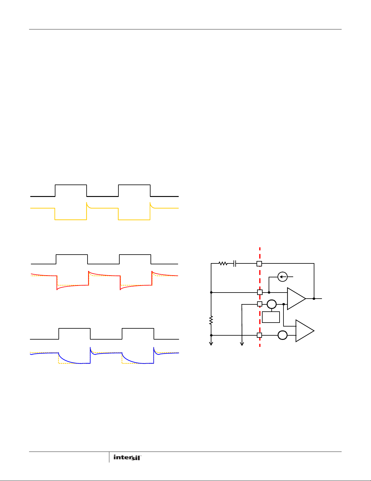
ISL6364
L/DCR OR ESL/R
MATCHING
SEN
Assuming the compensator design is correct, Figure 11 shows the
expected load transient response waveforms if L/DCR or
ESL/R
current I
is matching the R-C time constant. When the load
SEN
has a square change, the output voltage V
OUT
OUT
also
has a square response, except for the overshoot at load release.
However, there is always some PCB contact impedance of current
sensing components between the two current sensing points; it
hardly accounts into the L/DCR or ESL/R
matching calculation.
SEN
Fine tuning the matching is necessarily done in the board level to
improve overall transient performance and system reliability.
If the R-C timing constant is too large or too small, V
accurately represent real-time I
(s) and will worsen the
OUT
(s) will not
C
transient response. Figure 12 shows the load transient response
when the R-C timing constant is too small. V
OUT
will sag
excessively upon load insertion and may create a system failure
or early overcurrent trip. Figure 13 shows the transient response
when the R-C timing constant is too large. V
is sluggish in
OUT
drooping to its final value. There will be excessive overshoot if
load insertion occurs during this time, which may potentially hurt
the CPU reliability.
I
OUT
V
OUT
FIGURE 11. DESIRED LOAD TRANSIENT RESPONSE
WAVEFORMS
I
OUT
make an appropriate adjustment to the PWM duty cycle of each
channel with Intersil’s patented current-balance method.
Channel current balance is essential in achieving the thermal
advantage of multiphase operation. With good current balance,
the power loss is equally dissipated over multiple devices and a
greater area.
Voltage Regulation
The compensation network shown in Figure 14 assures that the
steady-state error in the output voltage is limited only to the error
in the reference voltage (DAC & OFFSET) and droop current
source, remote sense, and error amplifier.
The sensed average current I
will develop voltage drop across the resistor between FB and
for droop control. This current can be disconnected from the
V
OUT
FB node by tying R
high to VCC for non-droop applications.
FS_DRP
The output of the error amplifier, V
internal sawtooth waveforms to generate the PWM signals. The
PWM signals control the timing of the Intersil MOSFET drivers
and regulate the converter output to the specified reference
voltage.
The ISL6364 does not have a unity gain amplifier in between the
feedback path and error amplifier. For remote sensing, connect the
microprocessor sensing pins to the non-inverting input, FB, via the
feedback resistor (R
), and inverting input, RGND, of the error
FB
amplifier. This configuration effectively removes the voltage error
encountered when measuring the output voltage relative to the local
controller ground reference point. VSEN should connect to remote
sensing’s positive rail as well for over voltage protection.
EXTERNAL CIRCUIT
C
R
C
C
COMP
is tied to FB internally and
DROOP
, is compared to the
COMP
ISL6364
I
DROOP
V
OUT
FIGURE 12. LOAD TRANSIENT RESPONSE WHEN R-C TIME
CONSTANT IS TOO SMALL
I
OUT
V
OUT
FIGURE 13. LOAD TRANSIENT RESPONSE WHEN R-C TIME
CONSTANT IS TOO LARGE
Channel-Current Balance for VR0
The sensed current In from each active channel is summed
together and divided by the number of active channels. The
resulting average current I
load current. Channel current balance is achieved by comparing
the sensed current of each channel to the average current to
provides a measure of the total
AVG
ERROR
DAC
-
+
AMPLIFIER
-
+
-
OVP
+
V
COMP
FB
RGND
+
R
V
FB
DROOP
-
VSEN
V
OUT
FIGURE 14. OUTPUT VOLTAGE AND LOAD-LINE REGULATION
+
+
VID &
OFFSET
A digital-to-analog converter (DAC) generates a reference voltage,
which is programmable via SVID bus. The DAC decodes the SVID
set command into one of the discrete voltages shown in Table 4
on page 20. In addition, the output voltage can be margined in
±5mV step between -640mV and 635mV, as shown in Table 5 on
page 23, via SVID set OFFSET command (33h). For a finer than
5mV offset, a large ratio resistor divider can be placed on the FB
pin between the output and GND for positive offset or VCC for
negative offset.
VR1’s VSENS, RGNDS, FBS, and COMPS pins function in the
similar manner as VR0’s VSEN, RGND, FB, and COMP pins.
19
FN6861.0
December 22, 2010
Page 20
ISL6364
TABLE 4. VR12/IMVP7 VID 8-BIT
VID7 VID6 VID5 VID4 VID3 VID2 VID1 VID0 HEX VOLTAGE
0000000000OFF
00000001010.2500
00000010020.2550
00000011030.2600
00000100040.2650
00000101050.2700
00000110060.2750
00000111070.2800
00001000080.2850
00001001090.2900
000010100A0.2950
000010110B0.3000
000011000C0.3050
000011010D0.3100
000011100E0.3150
000011110F0.3200
00010000100.3250
00010001110.3300
00010010120.3350
00010011130.3400
00010100140.3450
00010101150.3500
00010110160.3550
00010111170.3600
00011000180.3650
00011001190.3700
000110101A0.3750
000110111B0.3800
000111001C0.3850
000111011D0.3900
000111101E0.3950
000111111F0.4000
00100000200.4050
00100001210.4100
00100010220.4150
00100011230.4200
00100100240.4250
00100101250.4300
00100110260.4350
00100111270.4400
TABLE 4. VR12/IMVP7 VID 8-BIT
VID7 VID6 VID5 VID4 VID3 VID2 VID1 VID0 HEX VOLTAGE
00101000280.4450
00101001290.4500
001010102A0.4550
001010112B0.4600
001011002C0.4650
001011012D0.4700
001011102E0.4750
001011112F0.4800
00110000300.4850
00110001310.4900
00110010320.4950
00110011330.5000
00110100340.5050
00110101350.5100
00110110360.5150
00110111370.5200
00111000380.5250
00111001390.5300
001110103A0.5350
001110113B0.5400
001111003C0.5450
001111013D0.5500
001111103E0.5550
001111113F0.5600
01000000400.5650
01000001410.5700
01000010420.5750
01000011430.5800
01000100440.5850
01000101450.5900
01000110460.5950
01000111470.6000
01001000480.6050
01001001490.6100
010010104A0.6150
010010114B0.6200
010011004C0.6250
010011014D0.6300
010011104E0.6350
010011114F0.6400
(Continued)
20
FN6861.0
December 22, 2010
Page 21
ISL6364
TABLE 4. VR12/IMVP7 VID 8-BIT
VID7 VID6 VID5 VID4 VID3 VID2 VID1 VID0 HEX VOLTAGE
01010000500.6450
01010001510.6500
01010010520.6550
01010011530.6600
01010100540.6650
01010101550.6700
01010110560.6750
01010111570.6800
01011000580.6850
01011001590.6900
010110105A0.6950
010110115B0.7000
010111005C0.7050
010111015D0.7100
010111105E0.7150
010111115F0.7200
01100000600.7250
01100001610.7300
01100010620.7350
01100011630.7400
01100100640.7450
01100101650.7500
01100110660.7550
01100111670.7600
01101000680.7650
01101001690.7700
011010106A0.7750
011010116B0.7800
011011006C0.7850
011011016D0.7900
011011106E0.7950
011011116F0.8000
01110000700.8050
01110001710.8100
01110010720.8150
01110011730.8200
01110100740.8250
01110101750.8300
01110110760.8350
01110111770.8400
(Continued)
TABLE 4. VR12/IMVP7 VID 8-BIT
VID7 VID6 VID5 VID4 VID3 VID2 VID1 VID0 HEX VOLTAGE
01111000780.8450
01111001790.8500
011110107A0.8550
011110117B0.8600
011111007C0.8650
011111017D0.8700
011111107E0.8750
011111117F0.8800
10000000800.8850
10000001810.8900
10000010820.8950
10000011830.9000
10000100840.9050
10000101850.9100
10000110860.9150
10000111870.9200
10001000380.9250
10001001890.9300
100010108A0.9350
100010118B0.9400
100011008C0.9450
100011018D0.9500
100011108E0.9550
100011118F0.9600
10010000900.9650
10010001910.9700
10010010920.9750
10010011930.9800
10010100940.9850
10010101950.9900
10010110960.9950
10010111971.0000
10011000981.0050
10011001991.0100
100110109A1.0150
100110119B1.0200
100111009C1.0250
100111019D1.0300
100111109E1.0350
100111119F1.0400
(Continued)
21
FN6861.0
December 22, 2010
Page 22
ISL6364
TABLE 4. VR12/IMVP7 VID 8-BIT
VID7 VID6 VID5 VID4 VID3 VID2 VID1 VID0 HEX VOLTAGE
10100000A01.0450
10100001A11.0500
10100010A21.0550
10100011A31.0600
10100100A41.0650
10100101A51.0700
10100110A61.0750
10100111A71.0800
10101000A81.0850
10101001A91.0900
10101010AA1.0950
10101011AB1.1000
10101100AC1.1050
10101101AD1.1100
10101110AE1.1150
10101111AF1.1200
10110000B01.1250
10110001B11.1300
10110010B21.1350
10110011B31.1400
10110100B41.1450
10110101B51.1500
10110110B61.1550
10110111B71.1600
10111000B81.1650
10111001B91.1700
10111010BA1.1750
10111011BB1.1800
10111100BC1.1850
10111101BD1.1900
10111110BE1.1950
10111111BF1.2000
11000000C01.2050
11000001C11.2100
11000010C21.2150
11000011C31.2200
11000100C41.2250
11000101C51.2300
11000110C61.2350
11000111C71.2400
(Continued)
TABLE 4. VR12/IMVP7 VID 8-BIT
VID7 VID6 VID5 VID4 VID3 VID2 VID1 VID0 HEX VOLTAGE
11001000C81.2450
11001001C91.2500
11001010CA1.2550
11001011CB1.2600
11001100CC1.2650
11001101CD1.2700
11001110CE1.2750
11001111CF1.2800
11010000D01.2850
11010001D11.2900
11010010D21.2950
11010011D31.3000
11010100D41.3050
11010101D51.3100
11010110D61.3150
11010111D71.3200
11011000D81.3250
11011001D91.3300
11011010DA1.3350
11011011DB1.3400
11011100DC1.3450
11011101DD1.3500
11011110DE1.3550
11011111DF1.3600
11100000E01.3650
11100001E11.3700
11100010E21.3750
11100011E31.3800
11100100E41.3850
11100101E51.3900
11100110E61.3950
11100111E71.4000
11101000E81.4050
11101001E91.4100
11101010EA1.4150
11101011EB1.4200
11101100EC1.4250
11101101ED1.4300
11101110EE1.4350
11101111EF1.4400
(Continued)
22
FN6861.0
December 22, 2010
Page 23
ISL6364
TABLE 4. VR12/IMVP7 VID 8-BIT
VID7 VID6 VID5 VID4 VID3 VID2 VID1 VID0 HEX VOLTAGE
11110000F01.4450
11110001F11.4500
11110010F21.4550
11110011F31.4600
11110100F41.4650
11110101F51.4700
11110110F61.4750
11110111F71.4800
11111000F81.4850
11111001F91.4900
11111010FA1.4950
11111011FB1.5000
11111100FC1.5050
11111101FD1.5100
11111110FE1.5150
11111111FF1.5200
TABLE 5. VR12/IMVP7 -640/+635mV OFFSET 8-BIT
OFS7 OFS6 OFS5 OFS4 OFS3 OFS2 OFS1 OFS0 HEX
0000000000
0000000101 5
000000100210
000000110315
000001000420
000001010525
000001100630
000001110735
000010000840
000010010945
000010100A50
000010110B55
000011000C60
000011010D65
000011100E70
000011110F75
000100001080
000100011185
000100101290
000100111395
(Continued)
VOLTAGE
(mV)
0
TABLE 5. VR12/IMVP7 -640/+635mV OFFSET 8-BIT
OFS7 OFS6 OFS5 OFS4 OFS3 OFS2 OFS1 OFS0 HEX
0001010014100
0001010115105
0001011016110
0001011117115
0001100018120
0001100119125
000110101A130
000110111B135
000111001C140
000111011D145
000111101E150
000111111F155
0010000020160
0010000121165
001000102217 0
001000112317 5
0010010024180
0010010125185
0010011026190
0010011127195
0010100028200
0010100129205
001010102A210
001010112B215
001011002C220
001011012D225
001011102E230
001011112F235
0011000030240
0011000131245
0011001032250
0011001133255
0011010034260
0011010135265
0011011036270
0011011137275
0011100038280
0011100139285
001110103A290
(Continued)
VOLTAGE
(mV)
23
FN6861.0
December 22, 2010
Page 24
ISL6364
TABLE 5. VR12/IMVP7 -640/+635mV OFFSET 8-BIT
OFS7 OFS6 OFS5 OFS4 OFS3 OFS2 OFS1 OFS0 HEX
001110113B295
001111003C300
001111013D305
001111103E310
001111113F315
0100000040320
0100000141325
0100001042330
0100001143335
0100010044340
0100010145345
0100011046350
0100011147355
0100100048360
0100100149365
010010104A370
010010114B375
010011004C380
010011014D385
010011104E390
010011114F395
0101000050400
0101000151405
0101001052410
0101001153415
0101010054420
0101010155425
0101011056430
0101011157435
0101100058440
0101100159445
010110105A450
010110115B455
010111005C460
010111015D465
010111105E470
010111115F475
0110000060480
0110000161485
(Continued)
VOLTAGE
(mV)
TABLE 5. VR12/IMVP7 -640/+635mV OFFSET 8-BIT
OFS7 OFS6 OFS5 OFS4 OFS3 OFS2 OFS1 OFS0 HEX
0110001062490
0110001163495
0110010064500
0110010165505
0110011066510
0110011167515
0110100068520
0110100169525
011010106A530
011010116B535
011011006C540
011011016D545
011011106E550
011011116F555
0111000070560
0111000171565
0111001072570
0111001173575
0111010074580
0111010175585
0111011076590
0111011177595
0111100078600
0111100179605
011110107A610
011110117B615
011111007C620
011111017D625
011111107E630
011111117F635
1000000080-640
1000000181-635
1000001082-630
1000001183-625
1000010084-620
1000010185-615
1000011086-610
1000011187-605
1000100038-600
(Continued)
VOLTAGE
(mV)
24
FN6861.0
December 22, 2010
Page 25
ISL6364
TABLE 5. VR12/IMVP7 -640/+635mV OFFSET 8-BIT
OFS7 OFS6 OFS5 OFS4 OFS3 OFS2 OFS1 OFS0 HEX
1000100189-595
100010108A-590
100010118B-585
100011008C-580
100011018D-575
100011108E-570
100011118F-565
1001000090-560
1001000191-555
1001001092-550
1001001193-545
1001010094-540
1001010195-535
1001011096-530
1001011197-525
1001100098-520
1001100199-515
100110109A-510
100110119B-505
100111009C-500
100111019D-495
100111109E-490
100111119F-485
10100000A0-480
10100001A1-475
10100010A2-470
10100011A3-465
10100100A4-460
10100101A5-455
10100110A6-450
10100111A7-445
10101000A8-440
10101001A9-435
10101010AA-430
10101011AB-425
10101100AC-420
10101101AD-415
10101110AE-410
10101111AF-405
(Continued)
VOLTAGE
(mV)
TABLE 5. VR12/IMVP7 -640/+635mV OFFSET 8-BIT
OFS7 OFS6 OFS5 OFS4 OFS3 OFS2 OFS1 OFS0 HEX
10110000B0-400
10110001B1-395
10110010B2-390
10110011B3-385
10110100B4-380
10110101B5-375
10110110B6-370
10110111B7-365
10111000B8-360
10111001B9-355
10111010BA-350
10111011BB-345
10111100BC-340
10111101BD-335
10111110BE-330
10111111BF-325
11000000C0-320
11000001C1-315
11000010C2-310
11000011C3-305
11000100C4-300
11000101C5-295
11000110C6-290
11000111C7-285
11001000C8-280
11001001C9-275
11001010CA-270
11001011CB-265
11001100CC-260
11001101CD-255
11001110CE-250
11001111CF-245
11010000D0-240
11010001D1-235
11010010D2-230
11010011D3-225
11010100D4-220
11010101D5-215
11010110D6-210
(Continued)
VOLTAGE
(mV)
25
FN6861.0
December 22, 2010
Page 26
ISL6364
TABLE 5. VR12/IMVP7 -640/+635mV OFFSET 8-BIT
OFS7 OFS6 OFS5 OFS4 OFS3 OFS2 OFS1 OFS0 HEX
11010111D7-205
11011000D8-200
11011001D9-195
11011010DA-190
11011011DB-185
11011100DC-180
11011101DD-175
11011110DE-170
11011111DF-165
11100000E0-160
11100001E1-155
11100010E2-150
11100011E3-145
11100100E4-140
11100101E5-135
11100110E6-130
11100111E7-125
11101000E8-120
11101001E9-115
11101010EA-110
11101011EB-105
11101100EC-100
11101101ED-95
11101110EE-90
11101111EF-85
11110000F0-80
11110001F1-75
11110010F2-70
11110011F3-65
11110100F4-60
11110101F5-55
11110110F6-50
11110111F7-45
11111000F8-40
11111001F9-35
11111010FA-30
11111011FB-25
11111100FC-20
11111101FD-15
(Continued)
VOLTAGE
(mV)
TABLE 5. VR12/IMVP7 -640/+635mV OFFSET 8-BIT
OFS7 OFS6 OFS5 OFS4 OFS3 OFS2 OFS1 OFS0 HEX
11111110FE-10
11111111FF -5
(Continued)
VOLTAGE
(mV)
Load-Line Regulation
Some microprocessor manufacturers require a precisely
controlled output resistance. This dependence of output voltage
on load current is often termed “droop” or “load line” regulation.
By adding a well controlled output impedance, the output voltage
can effectively be level shifted in a direction, which works to
achieve the load-line regulation required by these
manufacturers.
In other cases, the designer may determine that a more costeffective solution can be achieved by adding droop. Droop can
help to reduce the output-voltage spike that results from fast
load-current demand changes.
The magnitude of the spike is dictated by the ESR and ESL of the
output capacitors selected. By positioning the no-load voltage
level near the upper specification limit, a larger negative spike
can be sustained without crossing the lower limit. By adding a
well controlled output impedance, the output voltage under load
can effectively be level shifted down so that a larger positive
spike can be sustained without crossing the upper specification
limit.
As shown in Figure 14, a current proportional to the average
current of all active channels, I
line regulation resistor RFB. The resulting voltage drop across
is proportional to the output current, effectively creating an
R
FB
output voltage droop with a steady-state value defined, as shown
in Equation 13:
V
DROOPIAVG
=
R⋅
FB
The regulated output voltage is reduced by the droop voltage
V
. The output voltage as a function of load current is
DROOP
derived by combining Equation 13 with the appropriate sample
current expression defined by the current sense method
employed, as shown in Equation 14:
V
OUTVREF
where V
I
⎛⎞
---------------
–=
⎜⎟
⎝⎠
is the reference voltage (DAC), I
REF
LOAD
N
R
------------------R
R
ISEN
output current of the converter, R
connected to the ISEN+ pin, R
active channel number, and R
on the sensing method.
Therefore, the equivalent loadline impedance, i.e. Droop
impedance, is equal to Equation 15:
R
R
FB
------------
R
LL
X
------------------=
N
R
ISEN
The major regulation error comes from the current sensing
elements. To improve load-line regulation accuracy, a tight DCR
tolerance of inductor or a precision sensing resistor should be
considered.
, flows from FB through a load-
AVG
X
FB
is the total
LOAD
is the sense resistor
ISEN
is the feedback resistor, N is the
FB
is the DCR, or R
X
SENSE
(EQ. 13)
(EQ. 14)
depending
(EQ. 15)
26
FN6861.0
December 22, 2010
Page 27
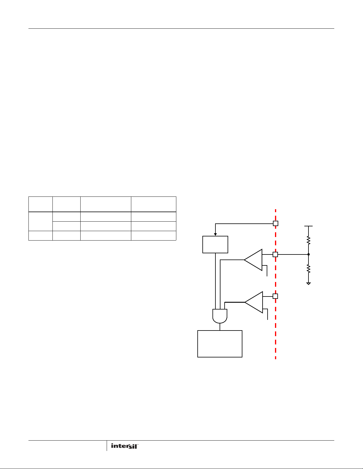
ISL6364
Output-Voltage Offset Programming
The output voltage can be margined in ±5mV steps between
-640mV and 635mV, as shown in Table 5, via SVID set OFFSET
command (33h). The minimum offset step is ±5mV. For a finer than
5mV offset, a large ratio resistor divider can be placed on the FB pin
between the output and GND for positive offset or VCC for negative
offset.
Dynamic VID
Modern voltage regulators need to make changes to their voltage
as part of normal operation. They direct the voltage regulator to
do this by making changes to the VID during regulator operation.
The power management solution is required to monitor the DAC
and respond to on-the-fly VID changes in a controlled manner.
Supervising the safe output voltage transition within the DAC
range of the processor or the load without discontinuity or
disruption is a necessary function of the voltage regulator.
Three different slew rates can be selected during Dynamic VID
(DVID) transition for VR0, but during VR0 soft-start, the setVID
SLOW rate is defaulted. FDVID has no impact on VR1 rail, which
can be 10mV/µs minimum rate for setVID Fast, 2.5mV/µs
minimum rate for setVID Slow.
TABLE 6. SLEW RATE OPTIONS
FDVID
VR0 0 10mV/µs 2.5mV/µs
1 20mV/µs 5.0mV/µs
VR1 DON’T CARE 10mV/µs 2.5mV/µs
SetVID FAST
(Minimum Rate)
SetVID SLOW
(Minimum Rate)
During dynamic VID transition and VID step up, the overcurrent
trip point increases by 140% to avoid falsely triggering OCP
circuits, while the overvoltage trip point will follow the
DAC+179mV level. If the dynamic VID occurs at PSI1/2/3/Decay
(low power state) asserted, the system should exit to PSI0 (full
power state) and complete the transition, and will not resume the
low power state operation unless the low power mode command
is asserted again.
In addition to ramping down the output voltage with a controlled
rate as previously described, both VR0 and VR1 can be
programmed into decay mode via SVID’s setDecay command.
Whenever the Decay command is received, the VR will enter PSI2
mode. The VR will be in single-phase operation. If the DE register
is selected to be “Enable”, the VR will operate in diode emulation
mode and drop to the target voltage at a decay rate determined
by the load impedance and output capacitive bank. The decay
rate will be limited to 2.5mV/µs rate setting. If the “DE” register
is selected to be “Disable”, then VR will drop at 2.5mV/µs rate
setting.
Operation Initialization
Prior to converter initialization, proper conditions must exist on
the enable inputs and VCC. When the conditions are met, the
controller begins soft-start. Once the output voltage is within the
proper window of operation, VR_RDY asserts logic high.
Enable and Disable
While in shutdown mode, the PWM outputs are held in a highimpedance state (or pulled to 40% of VCC) (or pulled to 40% of
VCC) to assure the drivers remain off. The following input
conditions must be met before the ISL6364 is released from
shutdown mode.
1. The bias voltage applied at VCC must reach the internal poweron reset (POR) rising threshold. Once this threshold is reached,
proper operation of all aspects of the ISL6364 is guaranteed.
Hysteresis between the rising and falling thresholds assure that
once enabled, ISL6364 will not inadvertently turn off unless the
bias voltage drops substantially (see “Electrical Specifications”
table beginning on page 8).
2. The ISL6364 features an enable input (EN_PWR) for power
sequencing between the controller bias voltage and another
voltage rail. The enable comparator holds the ISL6364 in
shutdown until the voltage at EN_PWR rises above 0.85V. The
enable comparator has about 100mV of hysteresis to prevent
bounce. It is important that the drivers reach their POR level
before the ISL6364 becomes enabled. The schematic in
Figure 15 demonstrates sequencing the ISL6364 with the
ISL66xx family of Intersil MOSFET drivers.
3. The voltage on EN_VTT must be higher than 0.85V to enable
the controller. This pin is typically connected to the output of
VTT VR.
ISL6364
POR
CIRCUIT
SOFT-START
AND
FAULT LOGIC
FIGURE 15. POWER SEQUENCING USING THRESHOLD-
SENSITIVE ENABLE (EN) FUNCTION
ENABLE
COMPARATOR
+
-
0.85V
+
-
0.85V
When all conditions previously mentioned are satisfied, ISL6364
begins the soft-start and ramps the output voltage to the Boot
Voltage set by hard-wired “BT” and “BTS” registers or first setVID
command if boot voltage set to zero volts. After remaining at
boot voltage for some time, ISL6364 reads the VID code via SVID
bus. If the VID code is valid, ISL6364 will regulate the output to
the final VID setting. If the VID code is “OFF” code, ISL6364 will
remain shut down.
EXTERNAL CIRCUIT
VCC
EN_PWR_CFP
EN_VTT
+12V
100kΩ
9.09kΩ
27
FN6861.0
December 22, 2010
Page 28
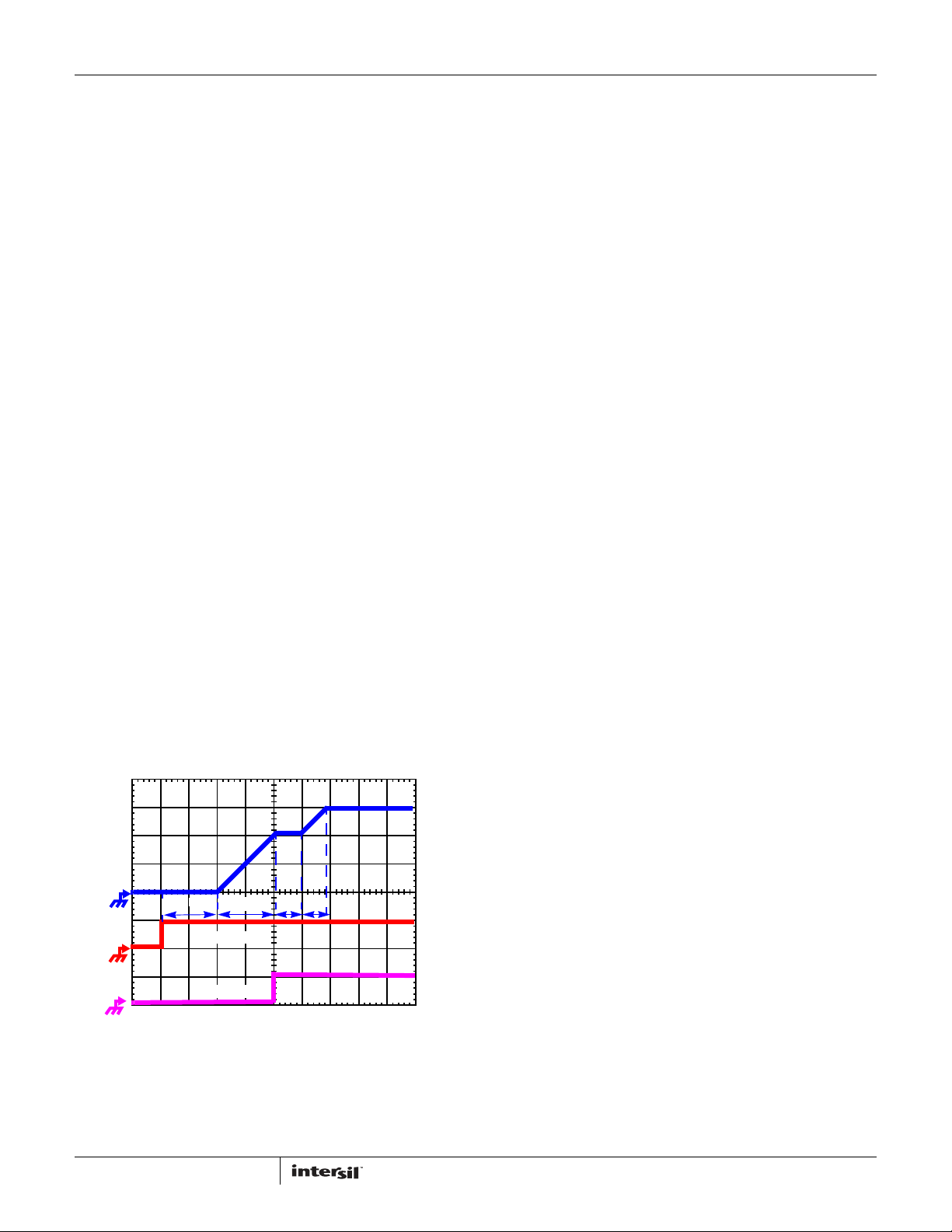
ISL6364
)
Soft-Start
ISL6364 based VR has 4 periods during soft-start, as shown in
Figure 16. After VCC, EN_VTT and EN_PWR reach their POR/enable
thresholds, the controller will have a fixed delay period t
delay period, the VR will begin first soft-start ramp until the output
voltage reaches V
voltage at a fixed slew rate, quarter of setVID
BOOT
FAST rate as in Table 6. Then, the controller will regulate the VR
voltage at V
for another period tD3 until SVID sends a new VID
BOOT
command. If the VID code is valid, ISL6364 will initiate the second
soft-start ramp at a slew rate, set by setVID FAST or SLOW
command in Table 6, until the voltage reaches the new VID voltage.
The soft-start time is the sum of the 4 periods, as shown in
Equation 16.
t
SStD1tD2tD3tD4
is a fixed delay with the typical value as 4.6ms. tD3 is
t
D1
+++=
determined by the time to obtain a valid new VID voltage from
the SVID bus. If the VID is valid before the output reaches the
boot voltage, the output will turn around to respond to the new
VID code.
During t
and tD4, ISL6364 digitally controls the DAC voltage
D2
change at 5mV per step. The soft-start ramp time tD2 and tD4
can be calculated based on Equations 17 and 18:
V
BOOT
----------------------------------------------------
t
D2
SetVID SLOW RATE
V
–
VIDVBOOT
-----------------------------------
t
D4
SetVID RATE
For example, when the V
at 10mV/µs, the first soft-start ramp time t
μs()=
μs()=
is set at 1.1V and SetVID rate is set
BOOT
will be around
D2
440µs and the second soft-start ramp time tD4 will be at
maximum of 40µs if an setVID command for 1.5V is received
after t
. However, if V
D3
is set at 0V, the first setVID
BOOT
command is for 1.5V, then tD2 will be around 150µs. Note that
the initial 0 to 250mV DAC is typically at a slower rate to
minimize the inrush current, the response time could be dictated
by the compensation network and the output filter.
. After this
D1
(EQ. 16)
(EQ. 17
(EQ. 18)
is proportional to the load current and the resistor value, as
shown in Equation 19:
R
V
IMON
where V
-------------------
=
IMON
between the IMON pin and GND, I
of the converter, R
ISEN+ pin, N is the active channel number, and R
R
IMON
N
X
------------------ I
R
ISEN
LOAD
is the voltage at the IMON pin, R
is the total output current
is the sense resistor connected to the
ISEN
LOAD
is the resistor
IMON
is the DC
X
(EQ. 19)
resistance of the current sense element, either the DCR of the
inductor or R
depending on the sensing method.
SENSE
The resistor from the IMON pin to GND should be chosen to
ensure that the voltage at the IMON pin is typically 900mV at the
maximum load current, typically corresponding to ICCMAX
register. The IMON voltage is linearly digitized every 132µs and
stored in the IOUT register (15h). When the IMON voltage reaches
900mV or beyond, the digitized IOUT will be FFh and the Alert pin
is pulled low to alarm the CPU. If the desired maximum load
current alert is not the exact ICCMAX value, the IMON resistor can
be scaled accordingly to make sure that it reaches 900mV at the
desired maximum output load.
R
IMON
0.9V R
ISEN
------------------------------
R
X
N
---------------------------------------=
I
DESIRED_MAX
(EQ. 20)
A small capacitor can be placed between the IMON pin and GND
to reduce the noise impact and do the average. The typical time
constant is 1ms for VR12 applications. If this pin is not used, tie
it to GND.
In addition, if the IMON pin voltage is higher than 1.12V,
overcurrent shutdown will be triggered, as described in
“Overcurrent Protection” on page 29.
Fault Monitoring and Protection
The ISL6364 actively monitors output voltage and current to detect
fault conditions. Fault monitors trigger protective measures to
prevent damage to a microprocessor load. One common powergood indicator is provided for linking to external system monitors.
The schematic in Figure 15 outlines the interaction between the
fault monitors and the VR_RDY signal.
t
t
D1
EN_VTT
VR_Ready
FIGURE 16. SOFT-START WAVEFORMS
t
D2
t
D3
D4
Current Sense Output
The current flowing out of the IMON pin is equal to the sensed
average current inside ISL6364. In typical applications, a resistor
is placed from the IMON pin to GND to generate a voltage, which
28
VR_Ready Signal
The VR_RDY pin is an open-drain logic output, which indicates
that the soft-start period is complete and the output voltage is
within the regulated range. VR_RDY is pulled low during
shutdown and releases high after a successful soft-start. VR_RDY
will be pulled low when an fault (OCP or OVP) condition is
detected, or the controller is disabled by a reset from EN_PWR,
EN_VTT, POR, or VID OFF-code. If the Multi_VR_config register is
set to 01h, then the VR_Ready line will stay high when receiving a
00h VID code after the first soft-start. The VR_RDYS behaves the
same as VR_RDY, and both are independent from each other.
However, the defaulted Multi_VR_config is 00h for VR0 and 01h
for VR1.
Overvoltage Protection
Regardless of the VR being enabled or not, the ISL6364
overvoltage protection (OVP) circuit will be active after its POR. The
OVP thresholds are different under different operation conditions.
When VR is not enabled and during the soft-start intervals t
December 22, 2010
, the
D1
FN6861.0
Page 29
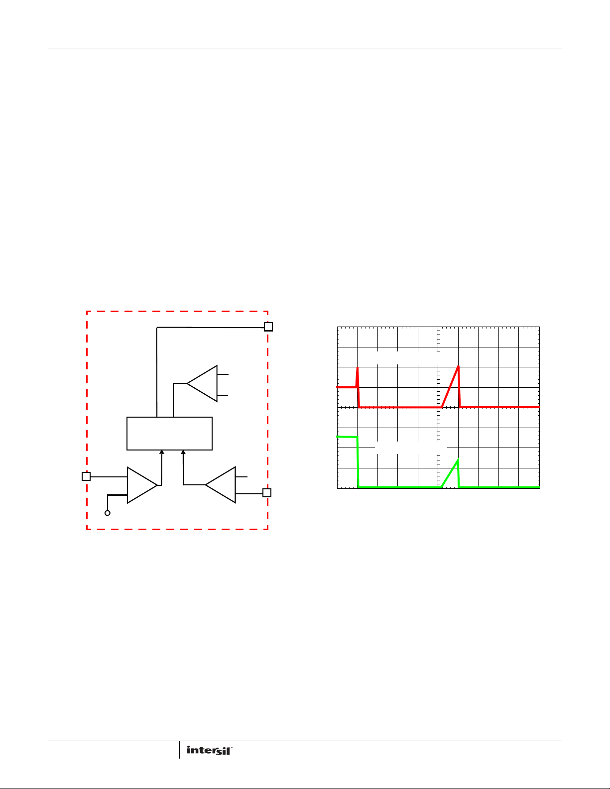
ISL6364
OVP threshold is 2.3V. Once the VR output voltage reaches above
the DAC, fires the first PWM and completes the soft-start, the OVP
trip point will change to a tacking level of DAC+179mV.
Two actions are taken by ISL6364 to protect the microprocessor
load when an overvoltage condition occurs.
At the inception of an overvoltage event, all PWM outputs are
commanded low instantly. This causes the Intersil drivers to turn on
the lower MOSFETs and pull the output voltage below a level to avoid
damaging the load. When the output voltage falls below the DAC
plus 107mV, PWM signals enter a high-impedance state (or pulled
to 40% of VCC). The Intersil drivers respond to the high-impedance
input by turning off both upper and lower MOSFETs. If the
overvoltage condition reoccurs, ISL6364 will again command the
lower MOSFETs to turn on. ISL6364 will continue to protect the load
in this fashion as long as the overvoltage condition occurs.
Once an overvoltage condition is detected, the respective VR#
ceases the normal PWM operation and pulls its VR_Ready low
until ISL6364 is reset. Cycling the voltage VCC below the
POR-falling threshold will reset the controller. Cycling the EN_VTT,
or EN_PWR will also reset the controller in ISL6364, but not in
ISL6364A.
VR_RDY
In instantaneous protection mode, ISL6364 utilizes the sensed
average current I
to detect an overcurrent condition. See
AVG
“Current Sensing” on page 16 for more details on how the
average current is measured. The average current is continually
compared with a constant 100µA reference current, as shown in
Figure 17. Once the average current exceeds the reference
current, a comparator triggers the converter to shutdown. In
addition, the current out of the IMON pin is equal to the sensed
average current I
. With a resistor from IMON to GND, the
AVG
voltage at the IMON will be proportional to the sensed average
current and the resistor value. The ISL6364 continuously monitors
the voltage at IMON pin. If the voltage at the IMON pin is higher
than 1.12V, a precision comparator triggers the overcurrent
shutdown. Since the internal current comparator has wider
tolerance than the voltage comparator, the IMON voltage
comparator is the preferred one for OCP trip. Hence, the resistor
between IMON and GND can be scaled such that the overcurrent
protection threshold is tripping lower than 100µA. For example,
the overcurrent threshold for the sensed average current I
AVG
can
be set to 95µA by using a 11.8kΩ resistor from IMON to GND.
Thus, the internal 100µA comparator might only be triggered at its
lower corner. However, IMON OCP trip should NOT be too far away
from 140µA, which is used for cycle-by-cycle protection and
inductor saturation.
100µA
+
OC
-
I
OC
AVG
1.12V
+
-
IMON
DAC
SOFT-START, FAULT
AND CONTROL LOGIC
VSEN
+
OV
-
ISL6364
VID + 0.179V
FIGURE 17. VR_RDY AND PROTECTION CIRCUITRY
Overcurrent Protection
ISL6364 has two levels of overcurrent protection. Each phase is
protected from a sustained overcurrent condition by limiting its
peak current, while the combined phase currents are protected on
an instantaneous basis.
For the individual channel overcurrent protection, ISL6364
continuously compares the sensed peak current (~50ns filter) signal
of each channel with the 140µA reference current. If one channel
current exceeds the reference current, ISL6364 will pull PWM signal
of this channel to low for the rest of the switching cycle. This PWM
signal can be turned on next cycle if the sensed channel current is
less than the 140µA reference current. The peak current limit of
individual channel will only use for cycle-by-cycle current limiting and
will not trigger the converter to shutdown.
OUTPUT CURRENT
0A
OUTPUT VOLTAGE
0V
FIGURE 18. OVERCURRENT BEHAVIOR IN HICCUP MODE. FSW =
500kHz
2ms/DIV
At the beginning of overcurrent shutdown, the controller places
all PWM signals in a high-impedance state (or pulled to 40% of
VCC), commanding the Intersil MOSFET driver ICs to turn off both
upper and lower MOSFETs. The system remains in this state a
period of 8ms. If the controller is still enabled at the end of this
wait period, it will attempt a soft-start. If the fault remains, the
trip-retry cycles will continue indefinitely (as shown in Figure 18)
until either controller is disabled or the fault is cleared. Note that
the energy delivered during trip-retry cycling is much less than
during full-load operation, so there is no thermal hazard during
this kind of operation
Thermal Monitoring (VR_HOT#)
VR_HOT# indicates the temperature status of the voltage
regulator. VR_HOT# is an open-drain output, and an external
pull-up resistor is required. This signal is valid only after the
controller is enabled.
29
FN6861.0
December 22, 2010
Page 30
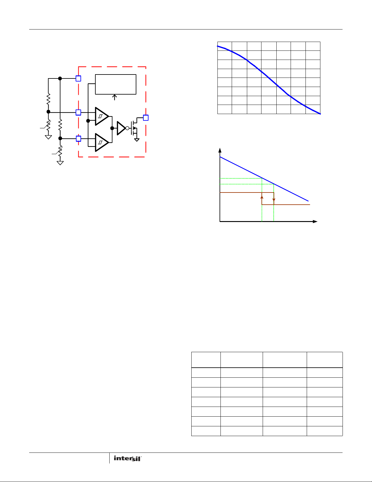
ISL6364
The VR_HOT# signal can be used to inform the system that the
temperature of the voltage regulator is too high and the CPU
should reduce its power consumption. The VR_HOT# signal may
be tied to the CPU’s PROC_HOT signal.
VCC
R
TM
TM
R
NTC1
o
c
R
TMS
TMS
R
o
NTC2
c
FIGURE 19. BLOCK DIAGRAM OF THERMAL MONITORING
FUNCTION
Thermal Trip
Point Lookup
Table (90-120
TMAX
+
-
+
-
NTC BETA ~ 3477
0
C)
ISL6364
VR_HOT#
The diagram of thermal monitoring function block is shown in Figure
19. One NTC resistor should be placed close to the respective power
stage of the voltage regulator VR0 and VR1 to sense the operational
temperature, and one pull-up resistor is needed to form the voltage
divider for the TM pin. As the temperature of the power stage
increases, the resistance of the NTC will reduce, resulting in the
reduced voltage at the TM pin. Figure 20 shows the TM voltage over
the temperature for a typical design with a recommended 6.8kΩ
NTC (P/N: NTHS0805N02N6801 from Vishay, β = 3477) and 1kΩ
resistor R
. It is recommended to use those resistors for the
TM
accurate temperature compensation since the internal thermal
digital code is developed based upon these two components. If a
different value is used, the temperature coefficient must be close to
3477 and R
must be scaled accordingly. For instance, say
TM
NTC = 10kΩ (β = 3477), then RTM should be 10kΩ/6.8kΩ*1kΩ =
1.47kΩ.
There is a comparator with hysteresis to compare the TM pin
voltage to the threshold set by the TMAX register for VR_HOT#
signal. With TMAX set at +100
°C, the VR_HOT# signal is pulled to
GND when either TM or TMS voltage is lower than 39.12% of VCC
voltage, and is open when both TM and TMS voltages increase to
above 40.98% of VCC voltage. The comparator trip point will be
programmable by TMAX values. Figure 20 shows the operation of
those signals.
100
90
80
70
(%)
CC
60
/V
TM
50
V
40
30
20
0 20 40 60 80 100 120 140
TEMPERATURE (
o
C)
FIGURE 20. THE RATIO OF TM VOLTAGE TO NTC TEMPERATURE
WITH RECOMMENDED PARTS
TM
40.98%*VCC
39.12%*VCC
VR_HOT#
TEMPERATURE
T1 T2
FIGURE 21. VR_HOT# SIGNAL (TMAX = +100°C) vs TM VOLTAGE
Based on the NTC temperature characteristics and the desired
threshold of the VR_HOT# signal, the pull-up resistor R
TM
of TM
pin is given by Equation 21:
R
1.557x R
TM
R
NTC(T2)
=
NTC T2()
is the NTC resistance at the VR_HOT# threshold
(EQ. 21)
temperature T2. The VR_HOT# is de-asserted at temperature T1,
as in Table 7. Since the NTC directly senses the temperature of
the PCB and not the exact temperature of the hottest component
on the board due to airflow and varied thermal impedance,
therefore, user should select a lower TMAX number, depending
upon the mismatching between NTC and the hottest
components, than such component to guarantee a safe
operation.
TAB LE 7. VR_HOT # TYPICAL T RIP POINT AND HYSTERESIS
TMAX
(°C)
90 88.6; 45.52% 85.9; 47.56% 2.7
95 94.3; 42.26% 91.4; 44.20% 2.9
100 100.0; 39.12% 97.1; 40.98% 2.9
105 106.1; 36.14% 103.0; 37.92% 3.1
110 109.1; 33.32% 106.1; 35.00% 3.0
115 115.5; 30.68% 112.3; 32.24% 3.2
120 118.7; 28.24% 115.5; 29.7% 3.2
VR_HOT# LOW (°C;
T2, %VCC)
VR_HOT# OPEN
(°C; T1, %VCC)
HYSTERESIS
(°C)
30
FN6861.0
December 22, 2010
Page 31
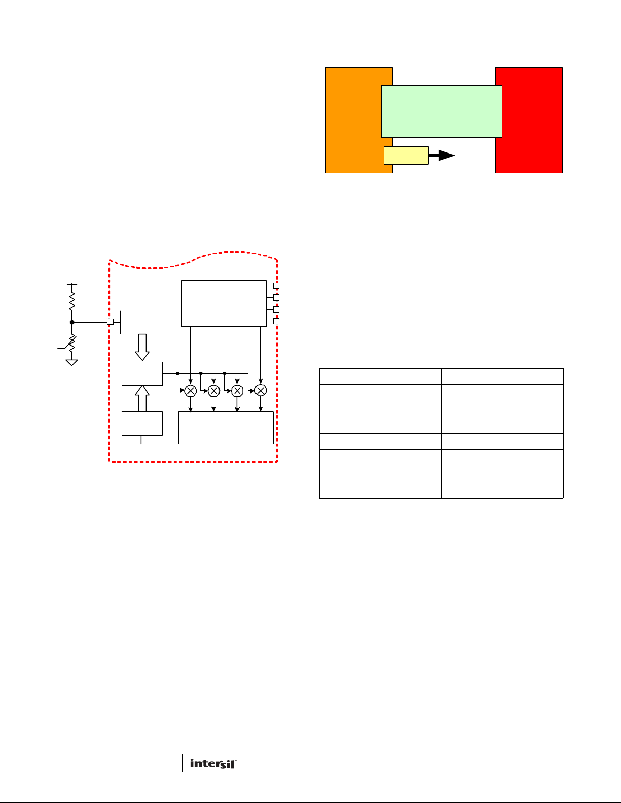
ISL6364
R
R
C
R
4
A
V
Temperature Compensation
The ISL6364 supports inductor DCR sensing, or resistive sensing
techniques. The inductor DCR has a positive temperature
coefficient, which is about +0.385%/°C. Since the voltage across
the inductor is sensed for the output current information, the
sensed current has the same positive temperature coefficient as
the inductor DCR.
In order to obtain the correct current information, there should be
a way to correct the temperature impact on the current sense
component. ISL6364 provides two methods: integrated
temperature compensation and external temperature
compensation.
The ISL6364 utilizes the voltage at the TM pin and “TCOMP”
register to compensate the temperature impact on the sensed
current. The block diagram of this function is shown in Figure 22.
CC
TM
o
c
NT
PLACE NTC
CLOSE TO
CHANNLE 1
FIGURE 22. BLOCK DIAGRAM OF INTEGRATED TEMPERATURE
ISL6364
TM
NON-LINEA
4-BIT
TCOMP
COMPENSATION
D/
A/D
CHANNEL
CURRENT
SENSE
/D
I
k
i
DROOP AND
OVERCURRENT
PRO TECTI ON
I
I
2
3
When the NTC is placed close to the current sense component
(inductor), the temperature of the NTC will track the temperature
of the current sense component. Therefore, the TM voltage can
be utilized to obtain the temperature of the current sense
component. Since NTC could pick up noise from the phase node,
a 0.1µF ceramic decoupling capacitor is recommended on the
TM pin in close proximity to the controller.
Based on the VCC voltage, the ISL6364 converts the TM pin
voltage to a 6-bit TM digital signal for temperature
compensation. With the non-linear A/D converter of ISL6364, the
TM digital signal is linearly proportional to the NTC temperature.
For accurate temperature compensation, the ratio of the TM
voltage to the NTC temperature of the practical design should be
similar to that in Figure 20.
I
sen4
I
sen3
I
sen2
I
sen1
I
1
VOUT
OUTPUT
INDUCTOR
PHASE1
POWER
STAGE
NTC
FIGURE 23. RECOMMENDED PLACEMENT OF NTC
Since the NTC attaches to the PCB, but not directly to the current
sensing component, it inherits high thermal impedance between
the NTC and the current sensing element. The “TCOMP” register
values can be utilized to correct the temperature difference
between NTC and the current sense component. As shown in
Figure 23, the NTC should be placed in proximity to the PSI
channel and the output rail; DON’T place it close to the MOSFET
side, which generates much more heat.
ISL6364 multiplexes the “TCOMP” value with the TM digital
signal to obtain the adjustment gain to compensate the
temperature impact on the sensed channel current. The
compensated channel current signal is used for droop and
overcurrent protection functions.
TABLE 8. “TCOMP” AND “TCOMPS” VALUES
TCOMP/TCOMPS (°C) TCOMP/TCOMPS (°C)
13 29.7
16 32.4
18.9 35.1
21.6 37.8
24.3 40.5
27 43.2
OFF
When a different NTC type or different voltage divider is used for the
TM function, the TCOMP voltage can also be used to compensate for
the difference between the recommended TM voltage curve in
Figure 20 and that of the actual design. If the same type NTC
(β = 3477) but different value is used, the pull-up resistor needs to
be scaled as shown in Equation 22:
1kΩ R
⋅
TM
6.8k Ω
NTC_NEW
--------------------------------------------=
R
(EQ. 22)
Design Procedure
1. Properly choose the voltage divider for the TM pin to match
the TM voltage vs temperature curve with the recommended
curve in Figure 20.
2. Run the actual board under the full load and the desired
cooling condition.
3. After the board reaches the thermal steady state, record the
temperature (T
or MOSFET) and the voltage at TM and VCC pins.
) of the current sense component (inductor
CSC
31
FN6861.0
December 22, 2010
Page 32
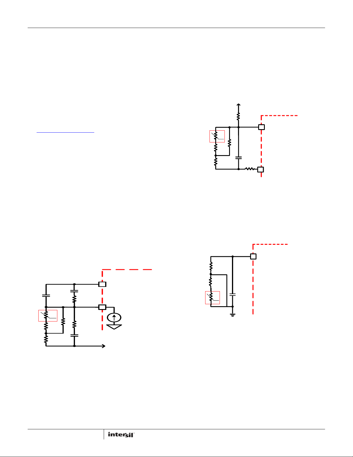
ISL6364
4. Use Equation 23 to calculate the resistance of the NTC, and
find out the corresponding NTC temperature T
from the
NTC
NTC datasheet or using Equation 24, where β is equal to 3477
for recommended NTC.
R
()
NTCTNTC
-------------------------------------------------------------------- -
T
NTC
⎛⎞
------------------------------- -
⎝⎠
R
NTCTNTC
TM
--------------------------=
VCCV–
TM
β
RTM
()
------------------ -
+ln
298.15
273.15–=
β
(EQ. 23)
(EQ. 24)
xR
V
TM
5. In Intersil designed worksheet, choose a number close to the
result as in Equation 25 in the “TCOMP” cell to calculate the
needed resistor network for the register “TCOMP” pin. (Note:
for worksheet, please contact Intersil Application support at
www.intersil.com/design/
T
COMPTCSCTNTC
–=
).
(EQ. 25)
6. Run the actual board under full load again with the proper
resistors connected to the “TCOMP” pin.
7. Record the output voltage as V1 immediately after the output
voltage is stable with the full load. Record the output voltage
as V2 after the VR reaches the thermal steady state.
8. If the output voltage increases over 2mV as the temperature
increases, i.e. V2 - V1 > 2mV, reduce “TCOMP” value; if the
output voltage decreases over 2mV as the temperature
increases, i.e. V1 - V2 > 2mV, increase “TCOMP” values.
External Temperature Compensation
When the “OFF” code of TCOMP is selected, then the internal
current source is not thermally compensated, i.e, the integrated
temperature compensation function is disabled. However, one
external temperature compensation network, shown in Figure
24, can be used to cancel the temperature impact on the droop
(i.e., load line).
the equivalent resistance between the FB pin and VOUT sensing
node inversely proportional to the temperature.
This external temperature compensation network can only
compensate the temperature impact on the droop, while it has no
impact to the sensed current inside ISL6364. Therefore, this
network cannot compensate for the temperature impact on the
overcurrent protection function. In addition, NTC could pick up
phase switching noise and easily inject into the loop. This method
is typically not recommended.
PHASE
ISENS-
o
C
ISL6364
ISENS+
FIGURE 25. NTC WITH L/DCR MATCHING NETWORK FOR
THERMAL COMPESNATION
Furthermore, the NTC can be placed with L/DCR matching
network to thermally compensate the sensed current, or with
IMON network to thermally compensate the IMON voltage
(typically need to set internal overcurrent trip higher than IMON
OCP trip), as shown in Figures 25 and 26, respectively. These
methods are typically applicable to both VR0 and VR1 for
non-droop applications.
IMON
COMP
ISL6364
FB
o
C
FIGURE 24. EXTERNAL TEMPERATURE COMPENSATION FOR
LOAD LINE
ID R O O P
VOUT
The sensed current will flow out of the FB pin and develop a droop
voltage across the resistor equivalent (R
and VOUT sensing node. If R
resistance reduces as the
FB
) between the FB pin
FB
temperature increases, the temperature impact on the droop can
be compensated. An NTC resistor can be placed close to the power
stage and used to form R
. Due to the nonlinear temperature
FB
characteristics of the NTC, a resistor network is needed to make
32
o
C
FIGURE 26. NTC WITH IMON NETWORK FOR THERMAL
COMPESNATION
ISL6364
Hard-wired Registers (Patent
Pending)
To set registers for VR12/IMVP7 applications using lowest pincount package and with lowest overall cost, Intersil has
developed a high resolution ADC using a patented technique with
simple 1%, 100ppm/k or better temperature coefficient resistor
divider, as shown in Figure 27. The same type of resistors are
preferred so that it has similar change over temperature. In
addition, the divider is comparing to the internal divider off VCC
and GND nodes and therefore must refer to VCC and GND pins,
not through any RC decoupling network.
FN6861.0
December 22, 2010
Page 33
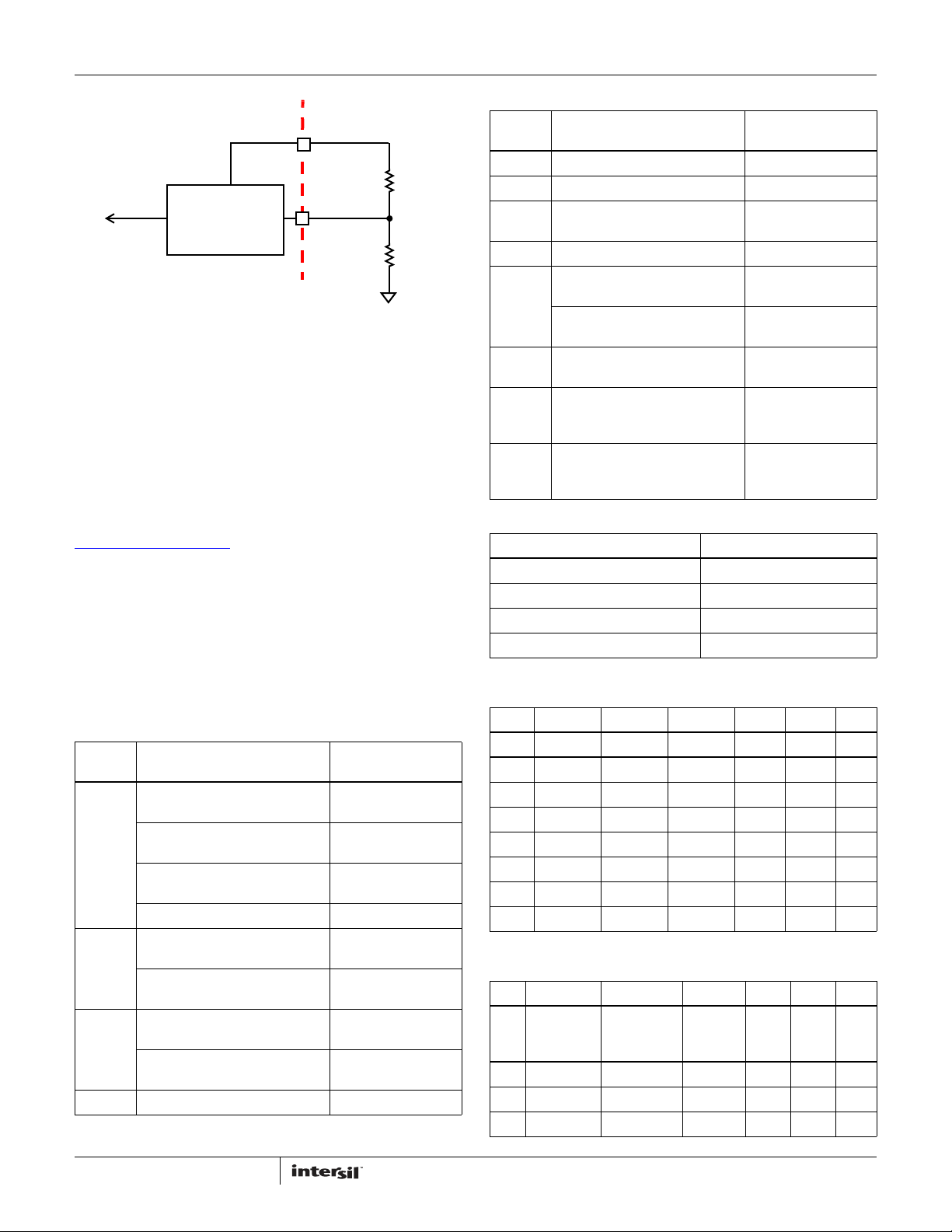
ISL6364
EXTERNAL CIRCUIT
ISL6364
REGISTER
TABLE
FIGURE 27. SIMPLIFIED RESISTOR DIVIDER ADC
ADC
VCC
R
UP
RDW
There are total of four register pins to program the system
parameters: Address OFFSET, setVID fast slew rate, boot voltage,
ICCMAX, diode emulation option, number of phase operation at
low power mode, and temperature compensation, as
summarized in Table 9. Prior to the soft-start, the system
parameters are stored in the SVID data registers of 0C, 0D, 0E,
and 0F, respectively, as shown in Table 10. They are reset by
Enable or VCC POR. In addition, data is available to verify that the
system setting is over a high volume production. A design
worksheet to select these pairs of resistors is available for use.
Please contact Intersil Application support at
www.intersil.com/design/
As an example, Table 11 shows the R
.
and RDW values of each
UP
pin for a specific system design; DATA for corresponding registers
can be read out via SVID’s Get(reg) command. In addition, as
shown in Table 12, some tie-high and tie-low options are for easy
programming and can also be used to validate the VR operation
during In-Circuit Test (ICT). For instance, when the system boot
voltage is required at zero Volts, the BT_XX or BTS_XX pin can be
tied to GND or VCC, prior to Enable, to get a known boot voltage
to check VR operation with ICT.
TABLE 9. SYSTEM PARAMETER DESCRIPTION
CODE
NAME DESCRIPTION RANGE
VR0/1 Address offset
(VR0 and VR1 Are In Operation)
VR0 Address offset (PWMS = VCC,
ADDR
BT
BTS
FDVID setVID Fast Slew Rate for VR0 10mV/µs, 20mV/µs
FSS_DRPS = 1 MΩ to GND)
VR0 Address offset (PWMS = VCC,
FSS_DRPS = 1 MΩ to VCC)
VR1 Address offset (PWM1 = VCC) 1, 3, 5, 7
VR0 Boot Voltages
(R
(R
(R
(R
TIED GND)
FS_DRP
VR0 Boot Voltages
TIED VCC)
FS_DRP
VR1 Boot Voltages
FSS_DRPS
VR1 Boot Voltages
FSS_DRPS
TIED GND)
TIED VCC)
0/1, 2/3 to 6/7
0, 2, 4, 6
8,A,C
0, 0.9, 1.0, 1.1V
0,1.2, 1.35, 1.5V
0, 0.9, 1.0, 1.1V
0, 0.85, 0.925, 1.05V
TABLE 9. SYSTEM PARAMETER DESCRIPTION
CODE
NAME DESCRIPTION RANGE
DE Diode Emulation Option of VR0 Enable, or Disable
DES Diode Emulation Option of VR1 Enable, or Disable
TMAX
IMAX Iccmax of VR0 15-165A (5/step)
IMAXS
NPSI
TCOMP
TCOMPS
REG R
0C ADDR IMAXS TMAX
0D BTS DES TCOMPS
0E BT FDVID TCOMP
0F NPSI DE IMAX
REG R
0C ADDR
Maximum Operating Temperature +90°C to +120°C
Iccmax of VR1
(R
FSS_DRPS
(R
FSS_DRPS
Number of Operational Phases in
PSI1/2/3/Decay States
Mismatching Temperature
Compensation between sensing
element and NTC for VR0
Mismatching Temperature
Compensation between sensing
element and NTC for VR1
TABLE 10. SYSTEM DATA REGISTER LOCATION
REGISTER PIN NAME DATA REGISTER CODE
ADDR_IMAXS_TMAX 0C
BTS_DES_TCOMPS 0D
BT_FDVID_TCOMP 0E
NPSI_DE_IMAX 0F
0/1 25A 100°C 29.4
0.85V ENABLED 29.7°C 255
1.1V 20mV/µs 29.7°C 10
SI1 ENABLED 100A OPEN 10
TABLE 12. TIE-HIGH AND TIE-LOW OPTIONS
0/1 35A/30A 100°C 10
0/1 20A/15A 95°C OPEN 10
6/7 35A/30A 100°C 499
TIED GND)
Iccmax of VR1
TIED VCC)
TABLE 11. DESIGN EXAMPLE
IMAXS
(R
GND/VCC)
FSS_DRPS
:
TMAX
(Continued)
(+5°C/Step)
20A, 25A, 30A, 35A
15A, 20A, 25A, 30A
1 or 2-Phase
OFF, +13°C to +43.2°C
OFF, +13°C to +43.2°C
R
UP
DW
kΩ 15kΩ 08h
kΩ 140kΩ C0h
kΩ OPEN DFh
kΩ 00h
UPRDW
kΩ OPEN 0h
kΩ 1Fh
kΩ OPEN C0h
DATA
DATA
33
FN6861.0
December 22, 2010
Page 34
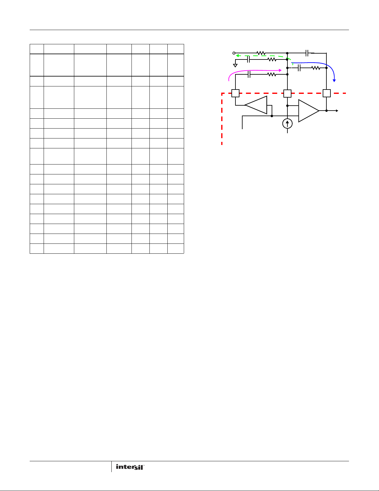
ISL6364
TABLE 12. TIE-HIGH AND TIE-LOW OPTIONS
REG R
IMAXS
(R
0C ADDR
6/7 20A/15A 95°C OPEN 499kΩ DFh
BTS
(R
FSS_DRPS
0D
GND/VCC)
1.1V/1.5V DISABLED +29.7°C OPEN 10
1.1V/1.5V ENABLED +29.7°C 10kΩ OPEN 1Fh
0 DISABLED +29.7°C OPEN 499
0 ENABLED +29.7°C 499
(R
BT
0E
0F NPSI DE IMAX
NOTE: Whenever 10kΩ is tie-high or tie-low, 0Ω can be used.
FS_DRP
GND/VCC)
1.1V/1.05V 10mV/µs +29.7°C OPEN 10
1.1V/1.05V 20mV/µs +29.7°C 10kΩ OPEN 1Fh
0 10mV/µs +29.7°C OPEN 499
0 20mV/µs +29.7°C 499
SI1/CI1 ENABLED 100A OPEN 10
SI1/CI1 ENABLED 165A 10
SI2/CI2 DISABLED 100A OPEN 499
SI2/CI2 DISABLED 165A 499kΩ OPEN DFh
GND/VCC)
:
:
:
FSS_DRPS
DES TCOMPS
FDVID TCOMP
TMAX
(Continued)
UPRDW
kΩ OPEN DFh
kΩ OPEN DFh
kΩ OPEN 1Fh
DATA
kΩ 00h
kΩ C0h
kΩ 00h
kΩ C0h
kΩ 00h
kΩ C0h
I
= I
DVC
R
VOUT
DVCS
V
DAC
FIGURE 28. DYNAMIC VID COMPENSATION NETWORK
FBS
I
RC
C
C
DVC
x1.333
R
I
DVC
R
DVC
IRC+I
ISL6364 INTERNAL CIRCUIT
C
C
C
FBS
-
+
DROOP_ACTUAL
I
C
R
C
ERROR
AMPLIFIER
COMPS
The amount of compensation current required is dependant on
the modulator gain of the system, K1, and the error amplifier R-C
components, R
and CC, that are in series between the FBS and
C
COMPS pins. Use Equations 26, 27, and 28 to calculate the RC
component values, R
DVC
and C
, for the VID-on-the-fly
DVC
compensation network. For these equations: VIN is the input
voltage for the power train; V
is the oscillator ramp
RAMP
amplitude as in Equation 3; and RC and CC are the error amplifier
R-C components between the FBS and COMPS pins.
K1
R
C
DVC
DVC
=
V
IN
------------------
V
RAMP
ARC⋅=
C
C
------
=
A
A
=
K1
----------------------------- -
3K11–()⋅
(EQ. 26)
(EQ. 27)
(EQ. 28)
Dynamic VID Compensation (DVC)
During a VID transition, the resulting change in voltage on the FBS
pin and the COMPS pin causes an AC current to flow through the
error amplifier compensation components from the FBS to the
COMPS pin. This current then flows through the feedback resistor,
, and can cause the output voltage to overshoot or undershoot
R
FBS
at the end of the VID transition. In order to ensure the smooth
transition of the output voltage during a VID change, a VID-on-the-fly
compensation network is required. This network is composed of a
resistor and capacitor in series, R
DVC
and C
and the FBS pin.
This VID-on-the-fly compensation network works by sourcing AC
current into the FBS node to offset the effects of the AC current
flowing from the FBS to the COMPS pin during a VID transition. To
create this compensation current, the controllers set the voltage
on the DVCS pin to be 4/3 of the voltage on the DAC. Since the
error amplifier forces the voltage on the FBS pin and the DAC to
be equal, the resulting voltage across the series RC between
DVCS and FBS is equal to the DAC voltage. The RC compensation
components, R
DVC
and C
, can then be selected to create the
DVC
desired amount of compensation current.
, between the DVCS
DVC
During DVID transitions, extra current builds up in the output
capacitors due to the C*dv/dt. The current is sensed by the
controller and fed across the feedback resistor creating extra
droop (if Enabled) and causing the output voltage not properly
tracking the DAC voltage. Placing a series R-C to ground from the
FB pin can sink this extra DVID induced current.
⋅
C
OUTRLL
---------------------------
=
C
R
FBS
C
⋅
OUTRLL
---------------------------
==
R
C
R
FBS
(EQ. 29)
(EQ. 30)
When the output voltage overshoots during DVID, the RDVC-CDVC
network can be used to compensate the movement of the
error-amplifier compensation network. When the output voltage
is lagging from DAC (or SVALERT#) or having a rough-off prior to
the final settling of DVID, the R-C network can be used to
compensate for the extra droop current generated by the
C*dv/dt. Sometimes, both networks can work together to
achieve the best result. In such case, both networks need to be
fine tuned in the board level for optimized performance.
Only VR1 is available for DVC compensation when the droop is
disabled, while the R-C network to compensate the lagging of
VOUT from DAC is applicable for both VR1 and VR0 when needed.
34
FN6861.0
December 22, 2010
Page 35

ISL6364
Disabling Output
When disabling any output, its respective pins should be tied
accordingly as in Table 13. However, when both outputs are fully
populated, pulling the respective PWM line to VCC should be
sufficient.
TABLE 13. DISABLE OUTPUT CONFIGURATION
DISABLE VR1 OUTPUT
PIN NAME PIN CONFIGURATION
PWMS VCC
RNGDS; VSENS;
FBS; IMONS;
ISENS-; VR_RDYS
HFCOMPS/DVCS;
ISENS+
FSS_DRPS 1MΩto GND (for 0,2,4,6 ADDR)
or 1MΩ to VCC for 8,A,C ADDR)
TMS Connect To TM pin or a 1/2 ratio Resistor Divider
(1MΩ/2MΩ) to avoid tripping VR_HOT#; or Use it
as a second thermal sensing for VR_HOT#. DON’T
DISABLE VR0 OUTPUT
PIN NAME PIN CONFIGURATION
PWM1 VCC
RNGD; VSEN;
FB; IMON;
ISEN[1:4]-; VR_RDY
HFCOMP; ISEN[1:6]+ OPEN
FS_DRP, RSET 1MΩ to GND
TM Connect To TMS pin or a 1/2 ratio Resistor Divider
(1MΩ/2MΩ) to avoid tripping VR_HOT#; or Use it
as a second thermal sensing for VR_HOT#. DON’T
GND
OPEN
tie it to VCC or GND.
GND
tie it to VCC or GND.
SVID Operation
The device is fully compliant with Intel VR12/IMVP7 SVID protocol
Rev 1.5, document# of 456098. To ensure proper CPU operation,
refer to this document for SVID bus design and layout guidelines;
each platform requires different pull-up impedance on the SVID bus,
while impedance matching and spacing among DATA, CLK, and
ALERT# signals must be followed. Common mistakes are insufficient
spacing among signals and improper pull-up impedance. A simple
operational instruction of SVID bus with Intel VTT Tool is documented
in “VR12 Design and Validation” in Table 15.
General Design Guide
This design guide is intended to provide a high-level explanation of
the steps necessary to create a multiphase power converter. It is
assumed that the reader is familiar with many of the basic skills
and techniques referenced in the following. In addition to this
guide, Intersil provides complete reference designs, which include
schematics, bills of materials, and example board layouts for
common microprocessor applications.
Power Stages
The first step in designing a multiphase converter is to determine
the number of phases. This determination depends heavily upon
the cost analysis, which in turn depends on system constraints
that differ from one design to the next. Principally, the designer
will be concerned with whether components can be mounted on
both sides of the circuit board; whether through-hole components
are permitted; and the total board space available for power
supply circuitry. Generally speaking, the most economical
solutions are those in which each phase handles between 15A
and 25A. All surface-mount designs will tend toward the lower
end of this current range. If through-hole MOSFETs and inductors
can be used, higher per-phase currents are possible. In cases
where board space is the limiting constraint, current can be
pushed as high as 40A per phase, but these designs require heat
sinks and forced air to cool the MOSFETs, inductors and heatdissipating surfaces.
MOSFETs
The choice of MOSFETs depends on the current each MOSFET will
be required to conduct; the switching frequency; the capability of
the MOSFETs to dissipate heat; and the availability and nature of
heat sinking and air flow.
Lower MOSFET Power Calculation
The calculation for heat dissipated in the lower MOSFET is
simple, since virtually all of the heat loss in the lower MOSFET is
due to current conducted through the channel resistance
(r
current; I
on page 14); d is the duty cycle (V
channel inductance.
An additional term can be added to the lower-MOSFET loss
equation to account for additional loss accrued during the dead
time when inductor current is flowing through the lower-MOSFET
body diode. This term is dependent on the diode forward voltage
at I
dead times, t
lower-MOSFET conduction interval respectively.
Finally, the power loss of output capacitance of the lower
MOSFET is approximated in Equation 33:
where C
the test voltage of V
the actual power dissipation will be slightly higher than this.
Thus the total maximum power dissipated in each lower MOSFET is
approximated by the summation of P
Upper MOSFET Power Calculation
In addition to r
losses are due to currents conducted across the input voltage (V
during switching. Since a substantially higher portion of the
). In Equation 31, IM is the maximum continuous output
DS(ON)
P
M
P
LOW 2,
P
LOW 3,
is the peak-to-peak inductor current (see Equation 1
LOW 1,
, V
PP
OUT/VIN
2
2
I
⎛⎞
I
PP
M
r
DS ON()
; the switching frequency, Fsw; and the length of
D(ON)
and td2, at the beginning and the end of the
d1
V
=
DON()FSW
2
1.5
---
3
OSS_LOW
C
⋅⋅ ⋅ ⋅≈
V
IN
OSS_LOWVDS_LOW FSW
is the output capacitance of the lower MOSFET at
DS_LOW
losses, a large portion of the upper-MOSFET
DS(ON)
----------+1d–()⋅=
⎜⎟
-----12
N
⎝⎠
I
I
⎛⎞
M
PP
------
---------+
⎝⎠
N
2
. Depending on the amount of ringing,
); and L is the per-
⎛⎞
I
M
t
⎜⎟
+
–
------
d1
N
⎝⎠
, P
LOW,1
LOW,2
I
PP
--------2
t
d2
and P
(EQ. 31)
(EQ. 32)
(EQ. 33)
LOW,3
.
IN
)
35
FN6861.0
December 22, 2010
Page 36

ISL6364
upper-MOSFET losses are dependent on switching frequency, the
power calculation is more complex. Upper MOSFET losses can be
divided into separate components involving the upper-MOSFET
switching times; the lower-MOSFET body-diode reverse-recovery
charge, Q
; and the upper MOSFET r
rr
conduction loss.
DS(ON)
When the upper MOSFET turns off, the lower MOSFET does not
conduct any portion of the inductor current until the voltage at
the phase node falls below ground. Once the lower MOSFET
begins conducting, the current in the upper MOSFET falls to zero
as the current in the lower MOSFET ramps up to assume the full
inductor current. In Equation 34, the required time for this
commutation is t
is P
.
UP,1
P
≈
UP 1,VIN
and the approximated associated power loss
1
I
M
⎛⎞
------
⎝⎠
N
t
I
⎛⎞
1
PP
---------+
2
----
⎜⎟
2
⎝⎠
F
SW
(EQ. 34)
At turn on, the upper MOSFET begins to conduct and this
transition occurs over a time t
power loss is P
≈
P
UP 2,VIN
.
UP,2
I
⎛⎞
I
M
⎜⎟
-----N
⎝⎠
⎛⎞
PP
---------
⎜⎟
–
2
⎝⎠
. In Equation 35, the approximate
2
t
2
F
----
SW
2
(EQ. 35)
A third component involves the lower MOSFET’s reverse-recovery
charge, Q
. Since the inductor current has fully commutated to the
rr
upper MOSFET before the lower-MOSFET’s body diode can draw all
, it is conducted through the upper MOSFET across VIN. The
of Q
rr
power dissipated as a result is P
and is approximated in
UP,3
Equation 36:
VINQrrF
=
P
UP 3,
SW
(EQ. 36)
The resistive part of the upper MOSFET’s is given in Equation 37
as P
.
UP,4
P
UP 4,rDS ON()
2
⎛⎞
I
M
⎜⎟
-----N
⎝⎠
2
I
PP
+ d⋅≈
---------12
(EQ. 37)
Equation 38 accounts for some power loss due to the drainsource parasitic inductance (L
, including PCB parasitic
DS
inductance) of the upper MOSFETs, although it is not the exact:
2
I
⎛⎞
I
PP
≈
P
UP 5,LDS
M
+
⎜⎟
---------
------
2
N
⎝⎠
(EQ. 38)
Finally, the power loss of output capacitance of the upper
MOSFET is approximated in Equation 39:
2
P
UP 6,
where C
⋅⋅ ⋅ ⋅≈
V
3
OSS_UP
IN
1.5
---
test voltage of V
C
OSS_UPVDS_UP FSW
is the output capacitance of lower MOSFET at
. Depending on the amount of ringing, the
DS_UP
(EQ. 39)
actual power dissipation will be slightly higher than this.
The total power dissipated by the upper MOSFET at full load can
now be approximated as the summation of the results from
Equations 34 to 39. Since the power equations depend on
MOSFET parameters, choosing the correct MOSFETs can be an
iterative process involving repetitive solutions to the loss
equations for different MOSFETs and different switching
frequencies.
Current Sensing Resistor
The resistors connected to the ISEN+ pins determine the gains in
the load-line regulation loop and the channel-current balance
loop as well as setting the overcurrent trip point. Select values for
these resistors by using Equation 40:
R
ISEN
where R
OCP
---------------------------
100 10
is the sense resistor connected to the ISEN+ pin, N
ISEN
------------=
–
6
N
×
(EQ. 40)
R
I
X
is the active channel number, RX is the resistance of the current
sense element, either the DCR of the inductor or R
depending on the sensing method, and I
overcurrent trip point. Typically, I
OCP
OCP
can be chosen to be 1.2
SENSE
is the desired
times the maximum load current of the specific application.
With integrated temperature compensation, the sensed current
signal is independent of the operational temperature of the
power stage, i.e. the temperature effect on the current sense
element R
is cancelled by the integrated temperature
X
compensation function. RX in Equation 40 should be the
resistance of the current sense element at the room
temperature.
When the integrated temperature compensation function is
disabled by selecting “OFF” TCOMP code, the sensed current will
be dependent on the operational temperature of the power
stage, since the DC resistance of the current sense element may
be changed according to the operational temperature. R
in
X
Equation 40 should be the maximum DC resistance of the
current sense element at the all operational temperature.
In certain circumstances, especially for a design with an
unsymmetrical layout, it may be necessary to adjust the value of
one or more ISEN resistors for VR0. When the components of one
or more channels are inhibited from effectively dissipating their
heat so that the affected channels run cooler than the average,
choose new, larger values of R
for the affected phases (see
ISEN
the section entitled “Current Sensing” on page 16). Choose
in proportion to the desired increase in temperature rise
R
ISEN,2
in order to cause proportionally more current to flow in the cooler
phase, as shown in Equation 41:
ΔT
R
ISEN,2RISEN
ΔR
ISENRISEN,2RISEN
In Equation 41, make sure that ΔT
----------=
ΔT
2
1
–=
is the desired temperature rise
2
(EQ. 41)
above the ambient temperature, and ΔT1 is the measured
temperature rise above the ambient temperature. Since all
channels’ R
(ΔR
) should be in series with the cooler channel’s ISEN+ pin
ISEN
are integrated and set by one RSET, a resistor
ISEN
to raise this phase current. While a single adjustment according to
Equation 41 is usually sufficient, it may occasionally be necessary
to adjust R
two or more times to achieve optimal thermal
ISEN
balance between all channels.
Load-Line Regulation Resistor
The load-line regulation resistor is labelled RFB in Figure 14. Its
value depends on the desired loadline requirement of the
application.
36
FN6861.0
December 22, 2010
Page 37

ISL6364
)
The desired loadline can be calculated using Equation 42:
V
R
where I
VR
DROOP
-------------------------=
LL
DROOP
I
FL
is the full load current of the specific application, and
FL
is the desired voltage droop under the full load
(EQ. 42)
condition.
Based on the desired loadline R
, the loadline regulation
LL
resistor can be calculated using Equation 43:
ISEN
R
R⋅
LL
X
is the sense resistor
ISEN
(EQ. 43)
N R⋅
R
---------------------------------------=
FB
where N is the active channel number, R
connected to the ISEN+ pin, and RX is the resistance of the
current sense element, either the DCR of the inductor or R
SEN
depending on the sensing method.
If one or more of the current sense resistors are adjusted for
thermal balance (as in Equation 41), the load-line regulation
resistor should be selected based on the average value of the
current sensing resistors, as given in Equation 44:
R
LL
--------- R
=
R
FB
where R
∑
R
ISEN(n)
ISEN n()
X
n
is the current sensing resistor connected to the
(EQ. 44
nth ISEN+ pin.
Output Filter Design
The output inductors and the output capacitor bank together to
form a low-pass filter responsible for smoothing the pulsating
voltage at the phase nodes. The output filter also must provide
the transient energy until the regulator can respond. Because it
has a low bandwidth compared to the switching frequency, the
output filter necessarily limits the system transient response. The
output capacitor must supply or sink load current while the
current in the output inductors increases or decreases to meet
the demand.
In high-speed converters, the output capacitor bank is usually the
most costly (and often the largest) part of the circuit. Output filter
design begins with minimizing the cost of this part of the circuit.
The critical load parameters in choosing the output capacitors are
the maximum size of the load step, ΔI; the load-current slew rate,
di/dt; and the maximum allowable output-voltage deviation under
transient loading, ΔV
to their capacitance, ESR, and ESL (equivalent series inductance).
At the beginning of the load transient, the output capacitors supply
all of the transient current. The output voltage will initially deviate by
an amount approximated by the voltage drop across the ESL. As the
load current increases, the voltage drop across the ESR increases
linearly until the load current reaches its final value. The capacitors
selected must have sufficiently low ESL and ESR so that the total
output-voltage deviation is less than the allowable maximum.
Neglecting the contribution of inductor current and regulator
response, the output voltage initially deviates by an amount, as
shown in Equation 45:
ΔVESL()
di
----- ESR()ΔI+≈
dt
. Capacitors are characterized according
MAX
(EQ. 45)
The filter capacitor must have sufficiently low ESL and ESR so
that ΔV < ΔV
MAX
.
Most capacitor solutions rely on a mixture of high-frequency
capacitors with relatively low capacitance in combination with
bulk capacitors having high capacitance but limited highfrequency performance. Minimizing the ESL of the highfrequency capacitors allows them to support the output voltage
as the current increases. Minimizing the ESR of the bulk
capacitors allows them to supply the increased current with less
output voltage deviation.
The ESR of the bulk capacitors also creates the majority of the
output-voltage ripple. As the bulk capacitors sink and source the
inductor AC ripple current (see “Interleaving” on page 13 and
Equation 2), a voltage develops across the bulk-capacitor ESR
equal to I
selected, the maximum allowable ripple voltage, V
(ESR). Thus, once the output capacitors are
C,PP
PP(MAX)
,
determines the lower limit on the inductance, as shown in
Equation 46.
V
K
⋅
OUT
L
----------------------------------------------------------
⋅≥
ESR
⋅
F
SWVIN
RCM
V⋅
PP MAX()
(EQ. 46)
Since the capacitors are supplying a decreasing portion of the
load current while the regulator recovers from the transient, the
capacitor voltage becomes slightly depleted. The output
inductors must be capable of assuming the entire load current
before the output voltage decreases more than ΔV
MAX
. This
places an upper limit on inductance.
Equation 47 gives the upper limit on L for the cases when the
trailing edge of the current transient causes a greater outputvoltage deviation than the leading edge. Equation 48 addresses
the leading edge. Normally, the trailing edge dictates the
selection of L because duty cycles are usually less than 50%.
Nevertheless, both inequalities should be evaluated, and L
should be selected based on the lower of the two results. In each
equation, L is the per-channel inductance, C is the total output
capacitance, and N is the number of active channels.
2NCV⋅
⋅⋅
L
--------------------------------------- ΔV
1.25
----------------------------- ΔV
≤
L
()
()
ΔI
NC⋅⋅
ΔI
OUT
2
MAX
2
ΔI ESR⋅–≤
MAX
ΔI ESR⋅– V
⎛⎞
–
INVOUT
⎝⎠
(EQ. 47)
(EQ. 48)
Switching Frequency Selection
There are a number of variables to consider when choosing the
switching frequency, as there are considerable effects on the
upper-MOSFET loss calculation. These effects are outlined in
“MOSFETs” on page 35, and they establish the upper limit for the
switching frequency. The lower limit is established by the
requirement for fast transient response and small output-voltage
ripple as outlined in “Output Filter Design” on page 37. Choose
the lowest switching frequency that allows the regulator to meet
the transient-response and output-voltage ripple requirements.
To minimize the effect of cross coupling between regulators,
select operating frequencies of VR0 and VR1 at least 50kHz
apart.
37
FN6861.0
December 22, 2010
Page 38
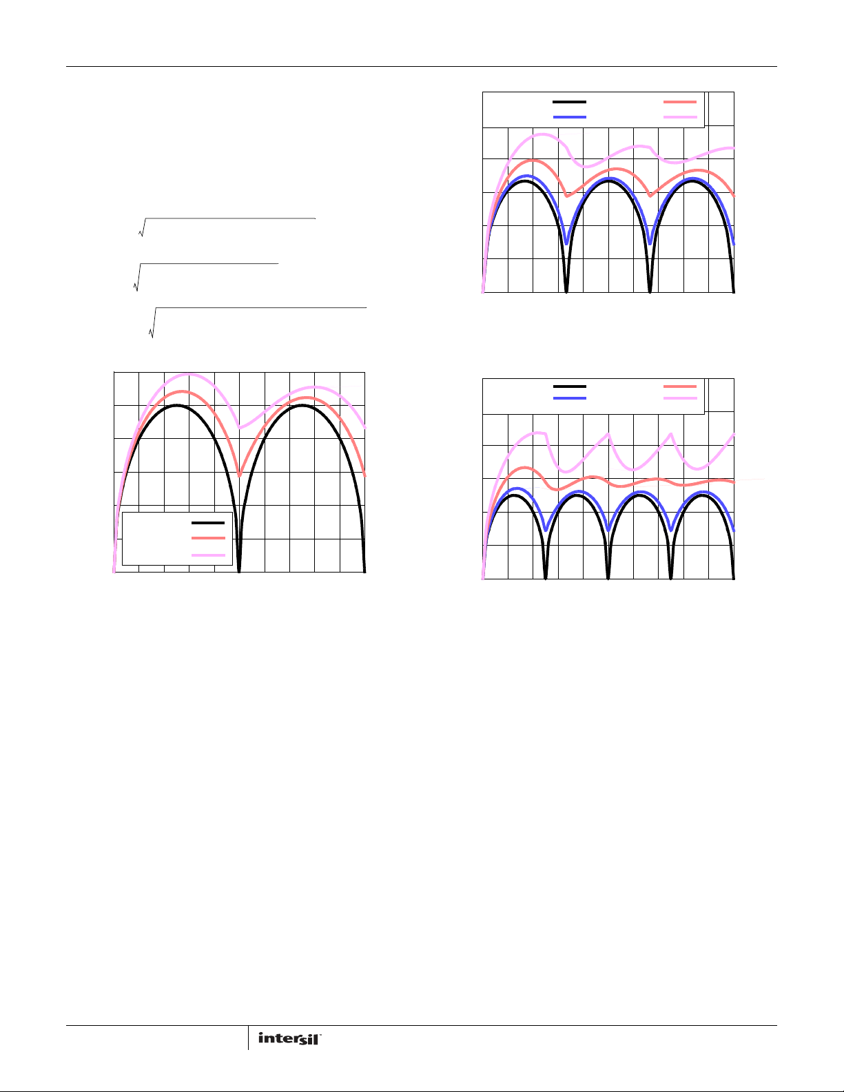
ISL6364
Input Capacitor Selection
The input capacitors are responsible for sourcing the AC
component of the input current flowing into the upper
MOSFETs. Their RMS current capacity must be sufficient to
handle the AC component of the current drawn by the upper
MOSFETs which is related to duty cycle and the number of
active phases. The input RMS current can be calculated with
Equation 49.
I
IN RMS,
K
IN CM,
K
RAMP CM,
2
K
IN CM,
ND• m– 1+()mND•–()•
-------------------------------------------------------------------------- -=
m2ND• m– 1+()
------------------------------------------------------------------------------------------------------------------=
0.3
)
O
/I
RMS
0.2
Io2• K
2
N
2
RAMP CM,
3
12N
2
I
•+=
Lo PP,
m1–()2mND•–()
+
2D2
(EQ. 49)
(EQ. 50)
3
(EQ. 51)
0.3
I
= 0
L,PP
)
O
I
RMS/
0.2
0.1
INPUT-CAPACITOR CURRENT (I
= 0.25 I
I
L,PP
0
00.4 1.00.2 0.6 0.8
O
DUTY CYCLE (V
I
L,PP
I
L,PP
= 0.5 I
= 0.75 I
OUT/VIN
O
O
)
FIGURE 30. NORMALIZED INPUT-CAPACITOR RMS CURRENT vs
DUTY CYCLE FOR 3-PHASE CONVERTER
0.3
I
= 0
L,PP
)
O
I
L,PP
= 0.25 I
O
I
RMS/
0.2
I
L,PP
I
L,PP
= 0.5 I
= 0.75 I
O
O
0.1
I
= 0
L,PP
= 0.5 I
I
L,PP
I
L,PP
INPUT-CAPACITOR CURRENT (I
0
00.4 1.00.2 0.6 0.8
= 0.75 I
O
O
DUTY CYCLE (V
OUT/VIN
)
FIGURE 29. NORMALIZED INPUT-CAPACITOR RMS CURRENT vs
DUTY CYCLE FOR 2-PHASE CONVERTER
For a 2-phase design, use Figure 29 to determine the input capacitor
RMS current requirement given the duty cycle, maximum sustained
output current (I
inductor current (I
), and the ratio of the per-phase peak-to-peak
O
) to IO. Select a bulk capacitor with a ripple
L,PP
current rating which will minimize the total number of input
capacitors required to support the RMS current calculated. The
voltage rating of the capacitors should also be at least 1.25 times
greater than the maximum input voltage.
0.1
INPUT-CAPACITOR CURRENT (I
0
00.4 1.00.2 0.6 0.8
DUTY CYCLE (V
OUT/VIN
)
FIGURE 31. NORMALIZED INPUT-CAPACITOR RMS CURRENT vs
DUTY CYCLE FOR 4-PHASE CONVERTER
Figures 27 and 28 provide the same input RMS current
information for 3 and 4-phase designs respectively. Use the
same approach to selecting the bulk capacitor type and number
as previously described.
Low capacitance, high-frequency ceramic capacitors are needed
in addition to the bulk capacitors to suppress leading and falling
edge voltage spikes. The result from the high current slew rates
produced by the upper MOSFETs turn on and off. Select low ESL
ceramic capacitors and place one as close as possible to each
upper MOSFET drain to minimize board parasitic impedances
and maximize noise suppression.
38
FN6861.0
December 22, 2010
Page 39
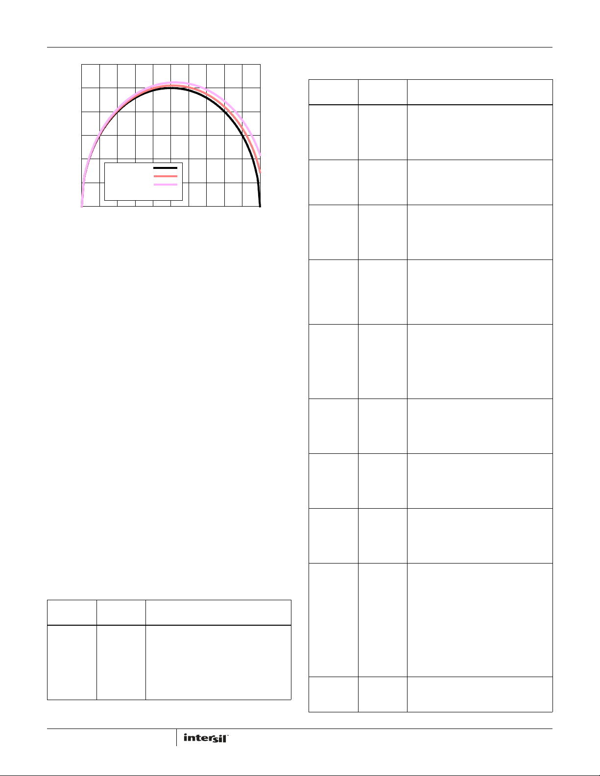
ISL6364
0.6
)
O
I
RMS/
0.4
0.2
INPUT-CAPACITOR CURRENT (I
0
FIGURE 32. NORMALIZED INPUT-CAPACITOR RMS CURRENT vs
I
= 0
L,PP
I
= 0.5 I
L,PP
I
L,PP
00.4 1.00.2 0.6 0.8
DUTY CYCLE FOR SINGLE-PHASE CONVERTER
O
= 0.75 I
O
DUTY CYCLE (V
OUT/VIN
)
MULTIPHASE RMS IMPROVEMENT
Figure 32 is provided as a reference to demonstrate the dramatic
reductions in input-capacitor RMS current upon the
implementation of the multiphase topology. For example,
compare the input RMS current requirements of a 2-phase
converter versus that of a single phase. Assume both converters
have a duty cycle of 0.25, maximum sustained output current of
40A, and a ratio of I
would require 17.3A
converter would only require 10.9A
to IO of 0.5. The single phase converter
L,PP
current capacity while the 2-phase
RMS
. The advantages become
RMS
even more pronounced when output current is increased and
additional phases are added to keep the component cost down
relative to the single phase approach.
Layout and Design Considerations
The following layout and design strategies are intended to minimize
the noise coupling, the impact of board parasitic impedances on
converter performance and to optimize the heat-dissipating
capabilities of the printed-circuit board. These sections highlight
some important practices which should follow during the layout
process. A layout check list in excel format is available for use.
Pin Noise Sensitivity, Design and Layout
Consideration
Table 14 below shows the noise sensitivity of each pin and their
design and layout consideration. All pins and external
components should not be across switching nodes and placed in
general proximity to the controller.
TABLE 14. PIN DESIGN AND/OR LAYOUT CONSIDERATION
NOISE
PIN NAME
EN_PWR No There is an internal 1µs filter. Decoupling
SENSITIVITY DESCRIPTION
capacitor is NOT needed, but if needed,
use a low time constant one to avoid too
mu ch o f sh ut- dow n de lay. It w ill als o be the
output of OVP function in ISL6364A: 34Ω
strong pull-up. 25 mils spacing from other
traces.
TABLE 14. PIN DESIGN AND/OR LAYOUT CONSIDERATION
(Continued)
NOISE
PIN NAME
RAMP_ADJ Yes NO decoupling capacitor allowed on this
RGND Yes Pairing up with the positive rail remote
VSEN No Used for Overvoltage protection sensing
FB Yes Pairing up with the negative rail of remote
HFCOMP Yes Connect an R to the VR0 output. The R
PSICOMP Yes The series impedance typically should be
COMP Yes Placing the compensation network in close
IMON Yes Referring to GND, not RGND. Place R and C
SVDATA;
SVCLK
SVALERT# No Open drain and high dv/dt pin during
SENSITIVITY DESCRIPTION
pin, but decoupling its resistor pull-up RAIL
with a high quality ceramic capacitor
(0.1µF or higher) or with very small RC
filter (<2.2µs).
sensing line that connected to FB resistor,
and routing them to the load sensing
points.
only, and it has 1µs internal filter.
Decoupling is NOT needed. Add a ZERO
Ohm series impedance to be compatible
with ISL6364A.
sensing line that connected to RGND, and
routing them to the load sensing points.
Reserve an RC from FB to GND to
compensate the output lagging from DAC
during DVID transitions.
value is typically equal or slightly higher
than the feedback resistor (droop resistor),
fine tuned according to the high frequency
transient performance. Placing the
compensation network in close proximity
to the controller.
2x-3x the impedance in type III
compensation to reduce noise coupling.
Placing the compensation network in close
proximity to the controller.
proximity to the controller. Typically use a
68pF or higher across FB to COMP
depending upon the noise coupling of the
layout.
in general proximity to the controller. The
time constant of RC should be sufficient,
typically 1ms, as an average function for
the digital IOUT of VR0.
Yes 13 to 26MHz signals when the SVID bus is
sending commands, pairing up with
SVALERT# and routing carefully back to
CPU socket. 20 mils spacing within
SVDATA, SVALERT#, and SVCLK; and more
than 30 mils to all other signals. Refer to
the Intel individual platform design
guidelines and place proper terminated
(pull-up) resistance for impedance
matching. Local decoupling capacitor is
needed for the pull-up rail.
transitions. Routing it in the middle of
SVDATA and SVCLK. Also see above.
39
FN6861.0
December 22, 2010
Page 40

ISL6364
TABLE 14. PIN DESIGN AND/OR LAYOUT CONSIDERATION
(Continued)
NOISE
PIN NAME
VR_RDY No Open drain and high dv/dt pin. Avoid its
IMONS Yes Referring to GND, not RGNDS. Place R and
VR_HOT# No Open drain and high dv/dt pin during
HFCOMPS/D
VCS
VR_RDYS No Open drain and high dv/dt pin. Avoid its
COMPS Yes Placing the compensation network in close
FBS Yes Pairing up with the negative rail of remote
VSENS No Used for Overvoltage protection sensing
RGNDS Pairing up with the positive rail remote
FSS_DDRS Yes Placing the R in close proximity to the
SENSITIVITY DESCRIPTION
pull-up higher than VCC. Tie it to ground
when not used.
C in general proximity to the controller. The
time constant of RC should be sufficient,
typically 1ms, as an average function for
the digital IOUT of VR1.
transitions. Avoid its pull-up rail higher
than VCC. 30 mils spacing from other
traces.
Yes Connect an R in similar value (equal or
slight higher) of the feedback resistor. If
programmed to be used as DVCS, Connect
an RC to FBS from this pin. Placing the
compensation network in close proximity
to the controller.
pu ll- up h igh er t han VCC . Ti e it to GND whe n
not used.
proximity to the controller. Typically use a
68pF or higher across FBS to COMPS
depending upon the noise coupling of the
layout.
sensing line that connected to RGNDS, and
routing them to the load sensing points.
Reserve an RC from FBS to GND to
compensate the output lagging from DAC
during DVID transitions.
only, and it has 1µs internal filter.
Decoupling is NOT needed. Add a series
impedance to be compatible with
ISL6364A.
sensing line that connected to FB resistor,
and routing them to the load sensing
points.
controller. Avoid using decoupling
capacitor on this pin. Must tie GND or VCC
via 1MΩ depending upon the desired
ADDRESS offset when VR1 is not in use.
Don’t use decoupling capacitor on this pin.
To minimize the effect of cross coupling
between regulators, select operating
frequencies of VR0 and VR1 at least 50kHz
apart.
TABLE 14. PIN DESIGN AND/OR LAYOUT CONSIDERATION
(Continued)
NOISE
PIN NAME
TMS Placing NTC in close proximity to the
ISENS+ Yes Connect to the output rail side of the
ISENS- Yes Connect to the phase node side of the
PWMS No Avoid the routing across or under other
ADDR_XX;
NPSI_XX;
BT_XX;
BTS_XX
TM Placing NTC in close proximity to the
SICI No Program SI (standard-inductor, tied to
RSET Yes Placing the R in close proximity to the
SENSITIVITY DESCRIPTION
output inductor of VR1 and to the output
rail, not close to MOSFET side (see Figure
23); the return trace should be 25 mils
away from other traces. Place 1k pull-up
and decoupling capacitor (typically 0.1µF)
in close proximity to the controller. The
pull-up resistor should be exactly tied to
the same point as VCC pin, not through an
RC filter. If not used, connect this pin to TM
or 1MΩ/2MΩ resistor divider, but DON’T
tie it to VCC or GND. Place the NTC in
proximity to the output rail, not close to
MOSFET side.
output inductor or current sensing resistor
pin with Isen resistor and decoupling
capacitor (27ns) placed in close proximity
to the controller.
output inductor or resistor pin with L/DCR
or ESL/R
proximity to the ISENS±- pins of the
controller. Differential pair with ISENS+
routing back to the controller.
phase’s power trains and DCR sensing
net wo rk . D on’ t m ak e t hem a cr os s o r und er
external components of the controller. At
least 30mils away from any other traces.
No Register setting is locked prior to soft start.
Since the external resistor-divider ratio
compares with the internal resistor ratio of
the VCC, their rail should be exactly tied to
the same point as VCC pin, not through an
RC filter. DON’T use decoupling capacitors
on these pins.
output inductor of VR0’s Channel 1 and to
the output rail, not close to MOSFET side
(see Figure 23); the return trace should be
25 mils away from other traces. Place 1k
pull-up and decoupling capacitor (typically
0.1µF) in close proximity to the controller.
The pull-up resistor should be exactly tied
to the same point as VCC pin, not through
an RC filter. If not used, connect this pin to
TMS or 1M Ω/2M Ω resistor divider, but
DON’T tie it to VCC or GND.
GND) and CI (coupled inductor, tied to
VCC). It is reserved for IAUTO in ISL6364A
and will be noise sensitive; SI and CI are
still programmable with this pin.
controller. DON’T use decoupling capacitor
on this pin.
matching network in close
SEN
40
FN6861.0
December 22, 2010
Page 41

ISL6364
TABLE 14. PIN DESIGN AND/OR LAYOUT CONSIDERATION
(Continued)
NOISE
PIN NAME
FS_DRP Yes Placing the R in close proximity to the
VCC Yes Place the decoupling capacitor in close
PWM1-4 NO Avoid the respective PWM routing across
EN_VTT No There is an internal 1µs filter. Decoupling
ISEN[4:1]+ Yes Connect to the output rail side of the
ISEN[4:1]- Yes Connect to the phase node side of the
GND Yes This EPAD is the return of PWM output
General
Comments
SENSITIVITY DESCRIPTION
controller. Must tie GND or VCC via 1MΩ
when VR0 is not in use. Don’t use
decoupling capacitor on this pin.
proximity to the controller.
or under other phase’s power
trains/planes and current sensing
network. Don’t make them across or under
external components of the controller. At
least 20mils away from any other traces.
capacitor is not needed, but if needed, use
a low timing constant one to avoid too
much shut-down delay.
respective channel’s output inductor or
resistor pin. Decoupling is optional and
might be required for long sense traces
and a poor layout.
respective channel’s output inductor or
resistor pin with L/DCR or ESL/R
matching network in close proximity to the
ISEN± pins of VR0. Differentially routing
back to the controller by paring with
respective ISEN+; at least 20 mils spacing
between pairs and away from other traces.
Each pair should not across or under the
other channel’s switching nodes [Phase,
UG ATE , LG ATE] an d powe r pl anes e ve n
though they are not in the same layer.
drivers and SVID bus. Use 4 or more vias to
directly connect the EPAD to the power
ground plane. Avoid using only single via or
0Ω resistor connection to the power
ground plane.
The layer next to the Top or Bottom layer is
preferred to be ground players, while the
signal layers can be sandwiched in the
ground layers if possible.
SEN
Component Placement
Within the allotted implementation area, orient the switching
components first. The switching components are the most critical
because they carry large amounts of energy and tend to generate
high levels of noise. Switching component placement should take
into account power dissipation. Align the output inductors and
MOSFETs such that space between the components is minimized
while creating the PHASE plane. Place the Intersil MOSFET driver
IC as close as possible to the MOSFETs they control to reduce the
parasitic impedances due to trace length between critical driver
input and output signals. If possible, duplicate the same
placement of these components for each phase.
Next, place the input and output capacitors. Position the highfrequency ceramic input capacitors next to each upper MOSFET
drain. Place the bulk input capacitors as close to the upper
MOSFET drains as dictated by the component size and
dimensions. Long distances between input capacitors and
MOSFET drains result in too much trace inductance and a
reduction in capacitor performance. Locate the output capacitors
between the inductors and the load, while keeping them in close
proximity to the microprocessor socket.
To improve the chance of first pass success, it is very important
to take time to follow the above outlined design guidelines and
Intersil generated layout check list, see more details in “VoltageReg ulator (VR) Design Materials” on pa ge 42. Proper planning for
the layout is as important as designing the circuits. Running
things in a hurry, you could be end up spending weeks and
months to debug a poorly-designed and improper-layout board.
Powering Up And Open-Loop Test
The ISL6364 features very easy debugging and powering up. For
the first-time powering up, an open-loop test can be done by
applying sufficient voltage (current limiting to 0.25A) to VCC,
proper pull-up to SVID bus, and signal high to EN_VTT and
EN_PWR pins with the input voltage (VIN) disconnected.
1. Each PWM output should operate at maximum duty cycle
(typically VR0 at 98% and VR1 at 83%) and correct switching
frequency.
2. The 0C, 0D, 0E, and 0F registers can be read via SVID bus to
check its proper setting if an VTT tool is installed and
operating.
3. If 5V drivers are used and share the same rail as VCC, the
proper switching on UGATEs and LGATEs should be seen.
4. If 12V drivers are used and can be disconnected from VIN and
sourced by an external 12V supply, the proper switching on
UGATEs and LGATEs should be observed.
5. If the above is not properly operating, you should check
soldering joint, resistor register setting, Power Train
connection or damage, i.e, shorted gates, drain and source.
Sometimes the gate might be measured short due to residual
gate charge. Therefore, a measured short gate with
ohmmeter cannot validate if the MOSFET is damaged unless
the Drain to Source is also measured short.
6. When the re-work is needed for the L/DCR matching network,
use an ohmmeter across the C to see if the correct R value is
measured before powering the VR up; otherwise, the current
imbalance due to improper re-work could damage the power
trains.
7. After everything is checked, apply low input voltage (1-5V)
with appropriate current limiting (~0.5A). All phases should
be switching evenly.
8. Remove the pull-up from EN_PWR pin, using bench power
supplies, power up VCC with current limiting (typically ~ 0.25A
if 5V drivers included) and slowly increase Input Voltage with
current limiting. For typical application, VCC limited to 0.25A,
VIN limited to 0.5A should be safe for powering up without no
load. High core-loss inductors likely need to increase the input
current limiting. All phases should be switching evenly.
41
FN6861.0
December 22, 2010
Page 42
ISL6364
Voltage-Regulator (VR) Design
Materials
The tolerance band calculation (TOB) worksheets for VR output
regulation and IMON have been developed using the Root-SumSquared (RSS) method with 3 sigma distribution point of the
related components and parameters. Note that the “Electrical
Specifications” table beginning on page 8 specifies no less than
6 sigma distribution point, not suitable for RSS TOB calculation.
To support VR design and layout, Intersil also developed a set of
worksheets and evaluation boards, as listed in Tables 15 and 16,
respectively. Contact Intersil’s local office or field support for the
latest available information.
TABLE 16. AVAILABLE VR12 EVALUATION BOARDS
EVALUATION BOARDS
ISL6366/67EVAL1
# OF
PHASES
6+1 - 7x7 60 Ld High-End Desktop and Server
# OF INTEGRATED
DRIVERS PACKAGE TARGETED APPLICATIONS I
TABLE 15. AVAILABLE DESIGN ASSISTANCE MATERIALS
Item Description
0 VR12 Design and Validation
1 VR12 Design Worksheet for Compensation and Component Selection
2 Transient Response Optimization Guidelines
3 VOUT and IMON TOB Calculator
4 SVID and PMBus Communication Tool
5 Resistor Register Calculator
6 Dynamic VID Compensation Calculator
7 VR12 Layout Design Guidelines
8 TCOMP and TM Selection Worksheet
9 Fine Tune OCP and Droop Worksheet
10 Evaluation Board Schematics in OrCAD Format and Layout in
Allegro Format
NOTE:
For worksheets, please contact Intersil Application support
at www.intersil.com/design/.
2
C/PMBUS
Yes 93%, 1.2V@50A 190A
PEAK
EFFICIENCY
with Discrete Drivers and
MOSFETs
PEAK
CURRENT
+25A
ISL6366/67EVAL2
ISL6364EVAL1
ISL6363EVAL1
ISL6353EVAL1
6+1 - 7x7 60 Ld High-End Desktop and Server
with DrMOS
4+1 - 6x6 48 Ld Desktop/Memory
4+1 2+1 7x7 60 Ld Desktop
3+0 2 5x5 40 Ld Memory
Yes 93.5%,
1.2V@50A
88%, 1.2V@50A 120A
88%, 1.2V@50A 120A
94%, 1.5V@25A 100A
190A
+25A
+35A
+35A
42
FN6861.0
December 22, 2010
Page 43

ISL6364
Revision History
The revision history provided is for informational purposes only and is believed to be accurate, but not warranted. Please go to web to make
sure you have the latest revision.
DATE REVISION CHANGE
12/22/10 FN6861.0 Initial Release.
Products
Intersil Corporation is a leader in the design and manufacture of high-performance analog semiconductors. The Company's products
address some of the industry's fastest growing markets, such as, flat panel displays, cell phones, handheld products, and notebooks.
Intersil's product families address power management and analog signal processing functions. Go to www.intersil.com/products
complete list of Intersil product families.
*For a complete listing of Applications, Related Documentation and Related Parts, please see the respective device information page
on intersil.com: ISL6364
To report errors or suggestions for this datasheet, please go to: www.intersil.com/askourstaff
FITs are available from our website at: http://rel.intersil.com/reports/sear
for a
For additional products, see www.intersil.com/product_tree
Intersil products are manufactured, assembled and tested utilizing ISO9000 quality systems as noted
Intersil products are sold by description only. Intersil Corporation reserves the right to make changes in circuit design, software and/or specifications at any time
without notice. Accordingly, the reader is cautioned to verify that data sheets are current before placing orders. Information furnished by Intersil is believed to be
accurate and reliable. However, no responsibility is assumed by Intersil or its subsidiaries for its use; nor for any infringements of patents or other rights of third
parties which may result from its use. No license is granted by implication or otherwise under any patent or patent rights of Intersil or its subsidiaries.
43
in the quality certifications found at www.intersil.com/design/quality
For information regarding Intersil Corporation and its products, see www.intersil.com
FN6861.0
December 22, 2010
Page 44
Package Outline Drawing
L48.6x6B
48 LEAD QUAD FLAT NO-LEAD PLASTIC PACKAGE
Rev 0, 9/09
6.00
6
PIN 1
INDEX AREA
ISL6364
A
B
4X
4.4
0.40
44X
37
36
48
6
PIN #1 INDEX AREA
1
(4X)
( 5. 75 TYP )
0.15
( 4. 40 )
TOP VIEW
TYPICAL RECOMMENDED LAND PATTERN
6.00
( 44 X 0 . 40 )
( 48X 0 . 20 )
( 48X 0 . 65 )
MAX 1.00
4 .40 ± 0.15
25
24
48X 0.45 ± 0.10
BOTTOM VIEW
SIDE VIEW
0 . 2 REF
C
0 . 00 MIN.
0 . 05 MAX.
5
12
13
4
0.10 CM
0.05 M
48X 0.20
BASE PLANE
AB
C
SEE DETAIL "X"
C
0.10
SEATING PLANE
C
0.08 C
DETAIL "X"
44
NOTES:
Dimensions are in millimeters.1.
Dimensions in ( ) for Reference Only.
2.
Dimensioning and tolerancing conform to AMSE Y14.5m-1994.
3.
Unless otherwise specified, tolerance : Decimal ± 0.05
4.
Dimension applies to the metallized terminal and is measured
between 0.15mm and 0.30mm from the terminal tip.
Tiebar shown (if present) is a non-functional feature.
5.
The configuration of the pin #1 identifier is optional, but must be
6.
located within the zone indicated. The pin #1 indentifier may be
either a mold or mark feature.
FN6861.0
December 22, 2010
 Loading...