

Page 1
®
ISL6341, ISL6341A, ISL6341B, ISL6341C
Data Sheet December 2, 2008
5V or 12V Single Synchronous Buck
Pulse-Width Modulation (PWM) Controller
The ISL6341, ISL6341A, ISL6341B, ISL6341C makes
simple work out of implementing a complete control and
protection scheme for a DC/DC stepdown converter driving
N-Channel MOSFET s in a synchronous buck topology . Since
it can work with either 5V or 12V supplies, this one family of
IC’s can be used in a wide variety of applications within a
system. It integrates the control, gate drivers, output
adjustment, monitoring and protection functions into a single
10 Ld Thin DFN package.
The ISL6341, ISL6341A, ISL6341B, ISL6341C (hereafter
referred to as “ISL6341x”, except as needed) provides single
feedback loop, voltage-mode control with fast transient
response. The output voltage can be precisely regulated to as
low as 0.8V, with a maximum tolerance of ±0.8%
over-temperature and line voltage variations. A fixed frequency
oscillator and wide duty cycle range reduces design complexity,
while balancing typical application cost and efficiency. The
frequency, duty cycle and OCP response are the only
differences among the ISL6341x versions. See Table 1.
Protection from overcurrent conditions is provided by
monitoring the r
of the lower MOSFET to inhibit PWM
DS(ON)
operation appropriately (see “Overcurrent Protec tion (OCP)”
on page 8 for details). This approach simplifies the
implementation and improves efficiency by eliminating the
need for a current sense resistor. The output voltage is also
monitored for undervoltage and overvoltage protection, in
addition to monitoring for a PGOOD output.
Ordering Information
PART NUMBER
(Note)
ISL6341ACRZ* 41AC 0 to +70 10 Ld 3x3 TDFN L10.3x3B
ISL6341BCRZ* 41BC 0 to +70 10 Ld 3x3 TDFN L10.3x3B
ISL6341CCRZ* 41CC 0 to +70 10 Ld 3x3 TDFN L10.3x3B
ISL6341CRZ* 341C 0 to +70 10 Ld 3x3 TDFN L10.3x3B
ISL6341AIRZ* 41AI -40 to +85 10 Ld 3x3 TDFN L10.3x3B
ISL6341BIRZ* 41BI -40 to +85 10 Ld 3x3 TDFN L10.3x3B
ISL6341CIRZ* 41CI -40 to +85 10 Ld 3x3 TDFN L10.3x3B
ISL6341IRZ* 6341 -40 to +85 10 Ld 3x3 TDFN L10.3x3B
ISL6341EVAL1Z Evaluation Board
*Add “-T” suffix for tape and reel. Please refer to TB347 for details on reel
specifications.
NOTE: These Intersil Pb-free plastic packaged products employ special
Pb-free material sets, molding compounds/die attach materials, and
100% matte tin plate plus anneal (e3 termination finish, which is RoHS
compliant and compatible with both SnPb and Pb-free soldering
operations). Intersil Pb-free products are MSL classified at Pb-free peak
reflow temperatures that meet or exceed the Pb-free requirements of
IPC/JEDEC J STD-020.
PART
MARKING
TEMP.
RANGE (°C)
PACKAGE
(Pb-free)
PKG.
DWG. #
FN6538.2
Features
• Operates from +4.5V to 14.4V Supply Voltage (for Bias)
- 1.5V to 12V V
Input Range (Up to 20V is Possible with
IN
Restrictions; see “Input Voltage Considerations” on
page 12)
- 0.8V to ~V
- Integrated Gate Drivers; LGATE Uses V
Output Range (Duty Cycle Limited)
IN
CC
(5V to 12V);
UGATE Uses External Boot Diode to (5V to 12V)
- 0.8V Internal Reference; ±0.8% Tolerance
• Simple Single-Loop Control Design
- Traditional Dual Edge Modulator
- Voltage-Mode PWM Control
- Drives N-Channel MOSFETs
• Fast Transient Response
- High-Bandwidth Error Amplifier
- 0% to 85% Max Duty Cycle for ISL6341, ISL6341C
- 0% to 75% Max Duty Cycle for ISL6341A, ISL6341B
• Lossless, Programmable Overcurrent Protection
- Uses Lower MOSFET’s r
DS(ON)
- Latch off mode (ISL6341, ISL6341B)
- Infinite Retry (Hiccup) Mode (ISL6341A)
- Infinite Retry (Hiccup) Mode; no UVP (ISL6341C)
• Output Voltage Monitoring
- Undervoltage and Overvoltage Shutdown
- PGOOD Output
• Small Converter Size in 10 Ld 3x3 Thin DFN
- 300kHz Fixed Oscillator (ISL6341, ISL6341C)
- 600kHz Fixed Oscillator (ISL6341A, ISL6341B)
- Fixed Internal Soft-Start, Capable into a Pre-biased
Load
- Enable/Shutdown Function on COMP/EN Pin
• Pb-Free (RoHS Compliant)
Applications
• Power Supplies for Microprocessors or Peripherals
- PCs, Servers, Memory Supplies
- DSP and Core Communications Processor Supplies
• Subsystem Power Supplies
- PCI, AGP; Graphics Cards; Digital TV
- SSTL-2 and DDR/DDR2/DDR3 SDRAM Bus
Termination Supply
• Cable Modems, Set-Top Boxes, and DSL Modems
• Industrial Power Supplies; General Purpose Supplies
• 5V or 12V-Input DC/DC Regulators
• Low-Voltage Distributed Power Supplies; Point of Load
1
CAUTION: These devices are sensitive to electrostatic discharge; follow proper IC Handling Procedures.
1-888-INTERSIL or 1-888-468-3774
| Intersil (and design) is a registered trademark of Intersil Americas Inc.
Copyright © Intersil Americas Inc. 2007, 2008. All Rights Reserved
All other trademarks mentioned are the property of their respective owners.
Page 2
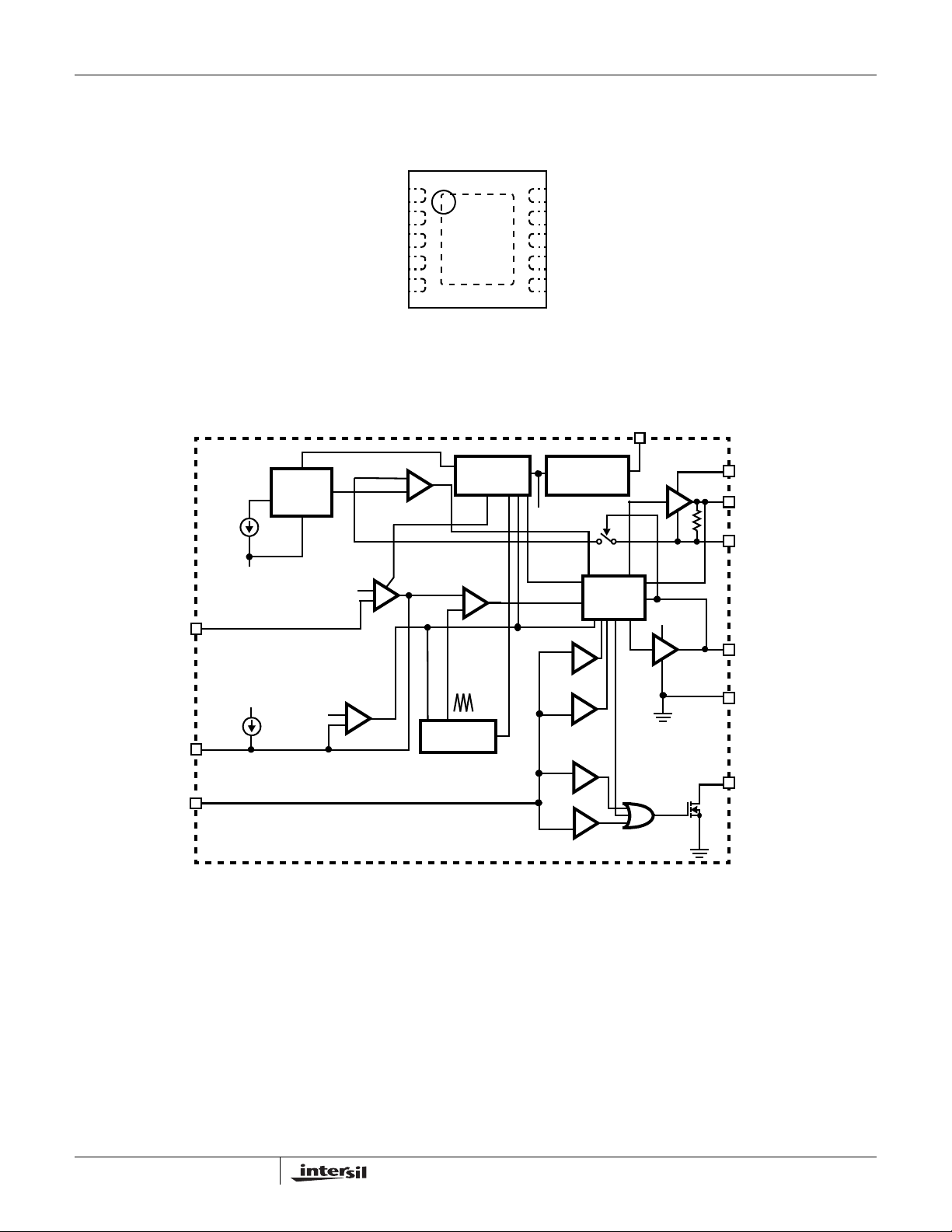
Pinout
ISL6341, ISL6341A, ISL6341B, ISL6341C
ISL6341, ISL6341A, ISL6341B, ISL6341C
(10 LD 3x3 TDFN)
TOP VIEW
Block Diagram
FB
10µA
TO
LGATE/OCSET
SAMPLE
AND
HOLD
BOOT
PHASE
UGATE
LGATE/OCSET
GND
COMPARATOR
ERROR
AMP
0.8V
+
-
OC
1
2
3
4
5
+
-
POR AND
SOFT-START
PWM
COMPARATOR
+
-
PGOOD
10
VOS
9
FB
8
COMP/EN
7
VCC
6
INTERNAL
REGULATOR
5V INT.
INHIBIT
PWM
+25%
CONTROL
LOGIC
EN
+
OV1
GATE
VCC
VCC
20kΩ
BOOT
UGATE
PHASE
LGATE/OCSET
COMP/EN
VOS
5V INT.
20µA
0.7V
-25%
+10%
-10%
+
+
-
-
+
-
UV1
OC
OV2
UV2
EN
-
+
OSCILLATOR
300kHz OR 600kHz
GND
PGOOD
2
FN6538.2
December 2, 2008
Page 3
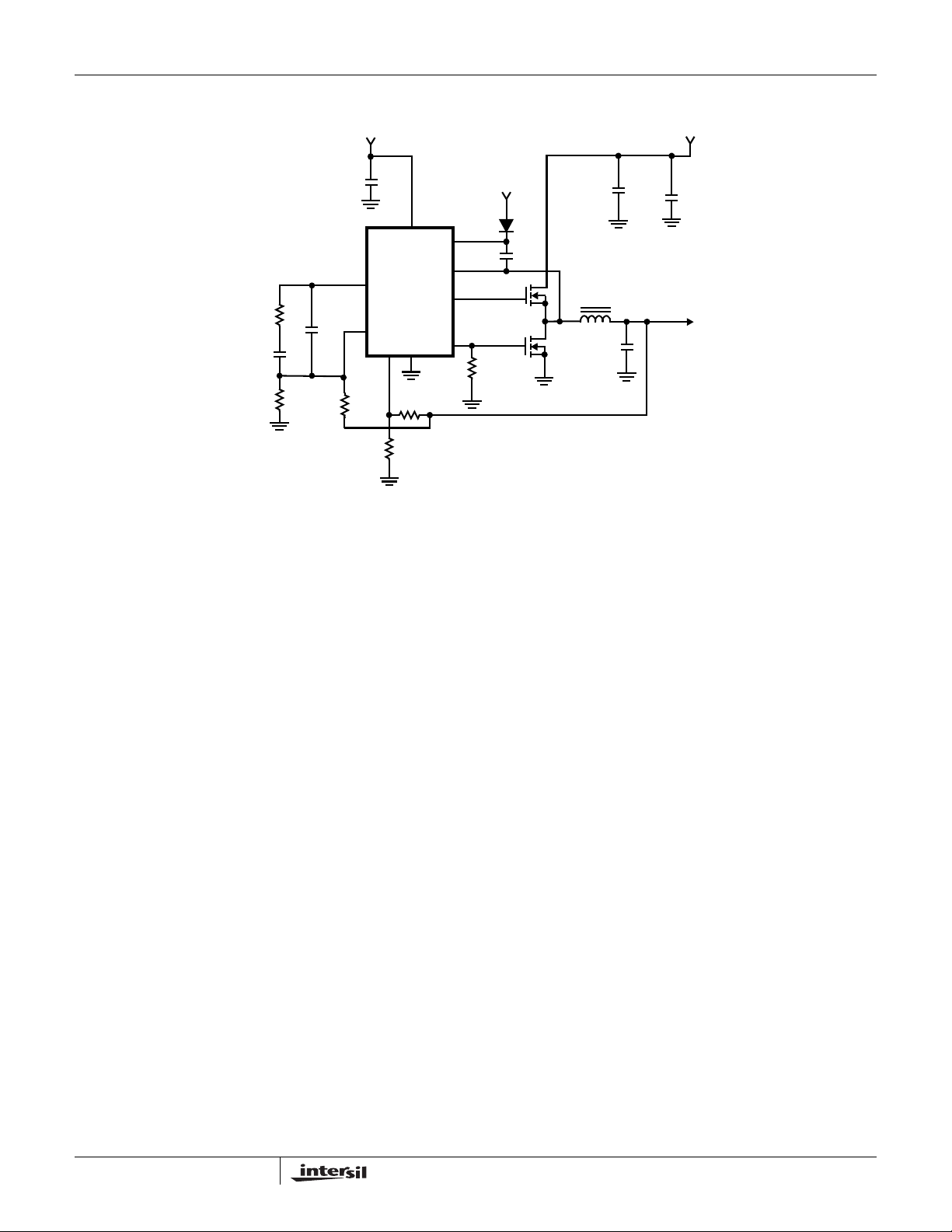
Typical Application
ISL6341, ISL6341A, ISL6341B, ISL6341C
TYPE II
COMPENSATION
SHOWN
R
F
C
F
R
OFFSET
C
DCPL
PGOOD
COMP/EN
FB
C
I
R
S
V
5V TO 12V
10
7
8
VOS
CC
VCC
6
ISL6341x
9
5
GND
R
VOS1
R
VOS2
5V TO 12V
BOOT
1
PHASE
2
UGATE
3
LGATE/OCSET
4
R
OCSET
V
1.5V TO 12V
V
GD
C
BOOT
L
OUT
C
OUT
IN
C
+V
BULK
O
C
HF
3
FN6538.2
December 2, 2008
Page 4
ISL6341, ISL6341A, ISL6341B, ISL6341C
Absolute Maximum Ratings Thermal Information
Supply Voltage, (VCC) . . . . . . . . . . . . . . . . . . . . GND - 0.3V to 15V
BOOT Voltage (V
BOOT to PHASE Voltage (V
BOOT-GND
). . . . . . . . . . . . . . . . GND - 0.3V to 36V
BOOT
- V
). . . GND - 0.3V to 15V
PHASE
-0.3V to 16V (<10ns, 10µJ)
UGATE Voltage (V
V
- 3.5V (<100ns Pulse Width, 2µJ) to V
PHASE
LGATE/OCSET Voltage (V
GND - 5V (<100ns Pulse Width, 2µJ) to V
PHASE Voltage (V
GND - 8V (<400ns, 20µJ) to 30V (<200ns, V
FB, VOS, COMP/EN Voltage. . . . . . . . . . . . . . . . . GND - 0.3V to 6V
). . . . . . .V
UGATE
LGATE
). . . . . . . . . .GND - 0.3V to V
PHASE
PHASE
). . . . . .GND - 0.3V to VCC + 0.3V
- 0.3V to V
BOOT-GND
BOOT
BOOT
CC
BOOT
+ 0.3V
+0.3V
+ 0.3V
+ 0.3V
<36V)
PGOOD Voltage. . . . . . . . . . . . . . . . . . . . . . . . . . .GND - 0.3V to 7V
CAUTION: Do not operate at or near the maximum ratings listed for extended periods of time. Exposure to such conditions may adversely impact product reliability and
result in failures not covered by warranty.
NOTES:
is measured with the component mounted on a high effective thermal conductivity test board in free air, with “direct attach” features. See
1. θ
JA
Tech Brief TB379 for details.
2. For θ
, the “case temp” location is the center of the exposed metal pad on the package underside.
JC
Thermal Resistance (Typical) θ
(°C/W) θJC (°C/W)
JA
10 Ld TDFN Package (Notes 1, 2). . . . 44 3.5
Maximum Power Dissipation. . . . . . . . . . . . . . . . . . . . . . . . . . . . . . 1.0W
Maximum Junction Temperature (Plastic Package) . . . . . . .+150°C
Maximum Storage Temperature Range. . . . . . . . . -65°C to +150°C
Pb-free Reflow Profile . . . . . . . . . . . . . . . . . . . . . . . . .see link below
http://www.intersil.com/pbfree/Pb-FreeReflow.asp
Operating Conditions
Supply Voltage Range, VCC . . . . . . . . . . . . . . . . . . . +4.5V to 14.4V
Ambient Temperature Range
ISL6341xCRZ (Commercial) . . . . . . . . . . . . . . . . . . 0°C to +70°C
ISL6341xIRZ (Industrial) . . . . . . . . . . . . . . . . . . . .-40°C to +85°C
Junction Temperature Range. . . . . . . . . . . . . . . . . .-40°C to +125°C
Electrical Specifications Test Conditions: V
limits are 100% tested at +25°C, unless otherwise specified. T emperature limit s established by characterization
= 12V, TJ = 0°C to +85°C, Unless Otherwise Noted. Parameters with MIN and/or MAX
CC
and are not production tested.
PARAMETER SYMBOL TEST CONDITIONS MIN TYP MAX UNITS
V
SUPPLY CURRENT
CC
Input Bias Supply Current I
Input Bias Supply Current I
VCC_disVCC
VCC_enVCC
= 12V; disabled 7.0 mA
= 12V; enabled (but not switching) 6.4 8.9 10.4 mA
POWER-ON RESET
Rising V
V
CC
POR Threshold V
CC
POR
POR Threshold Hysteresis 0.15 0.48 0.85 V
3.8 4.2 4.47 V
OSCILLATOR
Switching Frequency f
OSC
ISL6341C, ISL6341CC 270 300 330 kHz
ISL6341I, ISL6341CI 240 300 330 kHz
ISL6341AC, ISL6341BC 540 600 660 kHz
ISL6341AI, ISL6341BI 510 600 660 kHz
Ramp Amplitude (Note 3) ΔV
OSC
1.5 V
REFERENCE
Reference Voltage Tolerance V
REF
ISL6341C, ISL6341AC, ISL6341BC,
ISL6341CC
0.7936 0.8000 0.8064 V
ISL6341I, ISL6341AI, ISL6341BI, ISL6341CI 0.7920 0.8000 0.8080 V
ERROR AMPLIFIER
DC Gain (Note 3) GAIN 96 dB
Gain-Bandwidth Product (Note 3) GBWP 20 MHz
Slew Rate (Note 3) SR 8 V/µs
GATE DRIVERS
Upper Gate Source Impedance R
Upper Gate Sink Impedance R
Lower Gate Source Impedance R
Lower Gate Sink Impedance R
Upper Gate Source Impedance R
UG-SRChVCC
UG-SNKhVCC
LG-SRChVCC
LG-SNKhVCC
UG-SRClVCC
= 12V; I = 50mA 2.1 Ω
= 12V; I = 50mA 1.6 Ω
= 12V; I = 50mA 1.4 Ω
= 12V; I = 50mA 1.0 Ω
= 5V; I = 50mA 2.4 Ω
P-P
4
FN6538.2
December 2, 2008
Page 5
ISL6341, ISL6341A, ISL6341B, ISL6341C
Electrical Specifications Test Conditions: V
limits are 100% tested at +25°C, unless otherwise specified. T emperature limit s established by characterization
and are not production tested. (Continued)
PARAMETER SYMBOL TEST CONDITIONS MIN TYP MAX UNITS
Upper Gate Sink Impedance R
Lower Gate Source Impedance R
Lower Gate Sink Impedance R
PROTECTION/DISABLE
OCSET Current Source I
Enable Threshold (COMP/EN pin) V
VOS Rising Trip (PGOOD OV; +10%) 0.868 0.880 0.888 V
VOS Rising Trip (PGOOD OV) Hysteresis 16 mV
VOS Falling Trip (PGOOD UV; -10%) 0.708 0.720 0.732 V
VOS Falling Trip (PGOOD UV) Hysteresis 16 mV
VOS Rising Threshold (OV; +25%) 0.980 1.000 1.020 V
VOS Falling Threshold (UV; -25%)
(Note 5)
VOS Threshold (OV; 50% of V
VOS Bias Current VOS = 0.25V -1500 -250 -100 nA
PGOOD I
NOTES:
3. Limits should be considered typical and are not production tested.
4. Limits established by characterization and are not production tested.
5. The UVP is disabled on the ISL6341C; no trip point is measured.
) 0.380 0.400 0.410 V
OUT
UG-SNKlVCC
LG-SRClVCC
LG-SNKlVCC
OCSET
ENABLE
= 12V, TJ = 0°C to +85°C, Unless Otherwise Noted. Parameters with MIN and/or MAX
CC
= 5V; I = 50mA 1.7 Ω
= 5V; I = 50mA 1.5 Ω
= 5V; I = 50mA 1.1 Ω
LGATE/OCSET = 0V 9 10 11 µA
0.683 0.700 0.717 V
0.580 0.600 0.620 V
= 4mA 0.10 0.18 0.30 V
PGOOD
Functional Pin Description
VCC (Pin 6)
This pin provides the bias supply for the ISL6341x, as well
as the lower MOSFET’s gate. An internal regulator will
supply bias as VCC rises above 5V, but the LGATE/OCSET
will still be sourced by VCC. Connect a well-decoupled 5V to
12V supply to this pin.
FB (Pin 8)
This pin is the inverting input of the internal error amplifier. Use
FB, in combination with the COMP/EN pin, to compensate the
voltage-control feedback loop of the converter. A resistor divider
from V
VOS (Pin 9)
This input pin monitors the regulator output for OV and UV
protection, and PGOOD (OV and UV). Connect a resistor
divider from V
the FB resistor divider. It is not recommended to share one
divider for both FB and VOS; the response to a fault may not
be as quick or robust. There is a small pull-up bias current
on the pin; if the VOS pin is not connected, the OV protection
would be tripped to protect the load.
GND (Pin 5)
This pin represents the signal and power ground for the IC.
This pin is the high current connection, and should be tied to
the ground island/plane through the lowest impedance
to FB to GND is used to set the regulation voltage.
OUT
to VOS to GND, with the same ratio as
OUT
connection available. The metal pad under the package
should also be connected to the GND plane for thermal
conductivity, but does not conduct any current.
PHASE (Pin 2)
Connect this pin to the source of the upper MOSFET, and
the drain of the lower MOSFET. It is used as the sink for the
UGATE driver, and to monitor the voltage drop across the
lower MOSFET for overcurrent protection. This pin is also
monitored by the adaptive shoot-through protection circuitry
to determine when the upper MOSFET has turned off.
UGATE (Pin 3)
Connect this pin to the gate of upper MOSFET; it provides
the PWM-controlled gate drive. It is also monitored by the
adaptive shoot-through protection circuitry to determine
when the upper MOSFET has turned off.
BOOT (Pin 1)
This pin provides ground referenced bias voltage to the upper
MOSFET driver. A boot strap circuit is used to create a voltage
suitable to drive an N-Channel MOSFET (equal to V
GD
minus
the BOOT diode voltage drop), with respect to PHASE.
COMP/EN (Pin 7)
This is a multiplexed pin. During soft-start and normal converter
operation, this pin represents the output of the error amplifier.
Use COMP/EN, in combination with the FB pin, to compensate
the voltage-control feedback loop of the converter.
5
FN6538.2
December 2, 2008
Page 6
ISL6341, ISL6341A, ISL6341B, ISL6341C
Pulling COMP/EN low (V
ENABLE
= 0.7V nominal) will
disable the controller, which causes the oscillator to stop, the
LGA TE and UGATE outputs to be held low, and the soft-st art
circuitry to re-arm. The external pull-down device will initially
need to overcome up to 5mA of COMP/EN output current.
However, once the IC is disabled, the COMP output will also
be disabled, so only a 20µA current source will continue to
draw current.
When the pull-down device is released, the COMP/EN pin will
start to rise, at a rate determined by the 20µA charging up the
capacitance on the COMP/EN pin. When the COMP/EN pin
rises above the V
ENABLE
trip point, the ISL6341x will begin a
new initialization and soft-start cycle.
LGATE/OCSET (Pin 4)
Connect this pin to the gate of the lower MOSFET; it provides
the PWM-controlled gate drive (from V
). This pin is also
CC
monitored by the adaptive shoot-through protection circuitry to
determine when the lower MOSFET has turned off.
During a short period of time following Power-On Reset
(POR) or shut-down release, this pin is also used to
determine the overcurrent threshold of the converter.
Connect a resistor (R
) from this pin to GND. See
OCSET
“Overcurrent Protection (OCP)” on page 8 for equations. See
Table 1 for summary of overcurrent responses. Some of the
text describing the LGATE function may leave off the
OCSET part of the name when it is not relevant to the
discussion.
PGOOD (Pin 10)
This output is an open-drain pull-down device that reflects
the state of the PGOOD comparators. An external pull-up
resistor should be connected to a supply ≤6V. The output will
be held low through the soft-start ramp, and is allowed to go
high at the end of soft-start, if the VOS voltage is within its
window. The PGOOD window is tighter than the OV or UV
protection window, to give an early warning of a problem.
The PGOOD does respond directly to an OCP condition, but
may also go low if V
trip.
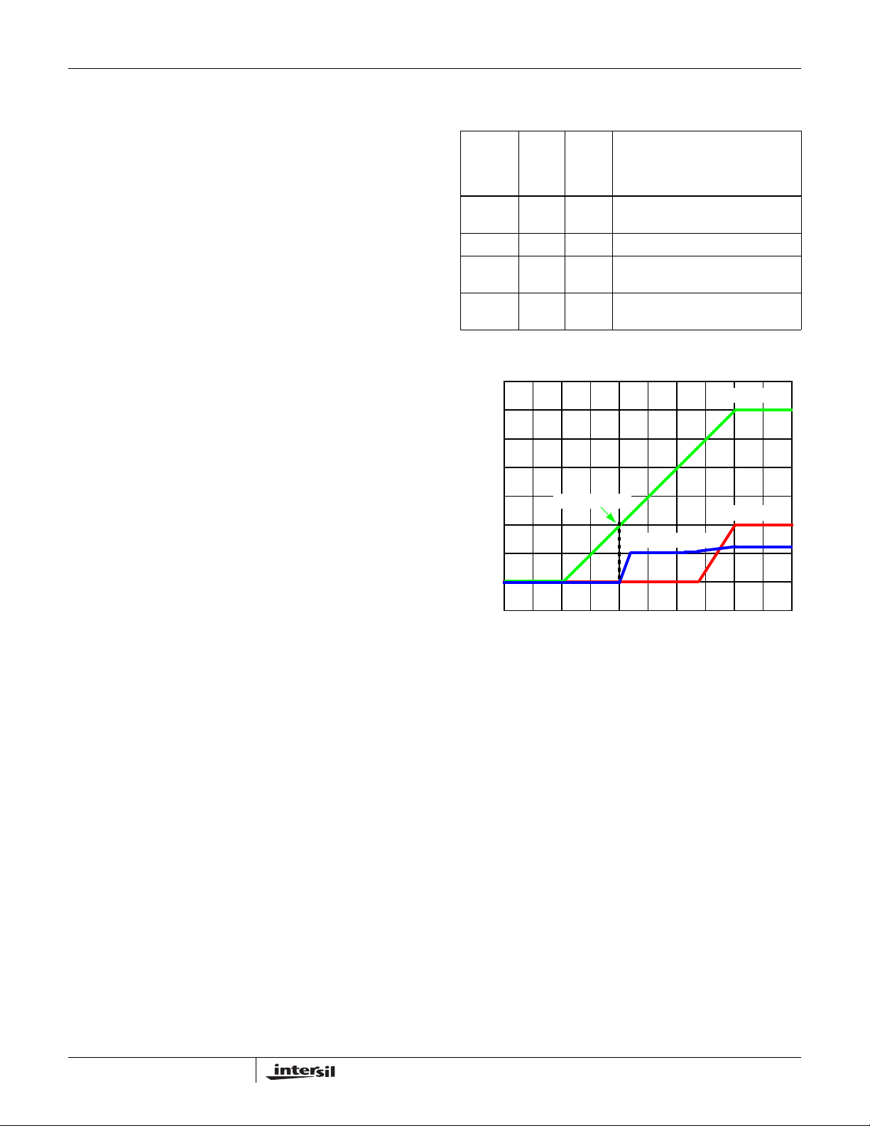
Figure 1 shows a simplified timing diagram. The
Power-On-Reset (POR) function continually monitors the
bias voltage at the VCC pin. Once the rising POR threshold
is exceeded (V
POR
initiates the Overcurrent Protection (OCP) sample and hold
operation (while COMP/EN is ~1V). When the sampling is
complete, V
OUT
drops low enough before an OCP
OUT
= 4.3V nominal), the POR function
begins the soft-start ramp.
Functional Description
TABLE 1. SUMMARY OF FEATURE DIFFERENCES
MAX
DUTY
PART
NUMBER
ISL6341 300 85 Latch off; toggle POR or COMP/EN
ISL6341A 600 75 “Hiccup” mode (infinite retries)
ISL6341B 600 75 Latch off; toggle POR or COMP/EN
ISL6341C 300 85 “Hiccup” mode (infinite retries); UVP
f
SW
(kHz)
CYCLE
(%)
(OVERCURRENT PROTECTION)
to restart
to restart
is disabled
Initialization (POR and OCP Sampling)
~4.3V POR
COMP/EN (1V/DIV)
GND>
GND>
GND>
GND>
FIGURE 1. POR AND SOFT-START OPERATION
If the COMP/EN pin is held low during power-up, that will just
delay the initialization until it is released and the COMP/EN
voltage is above the V
ENABLE
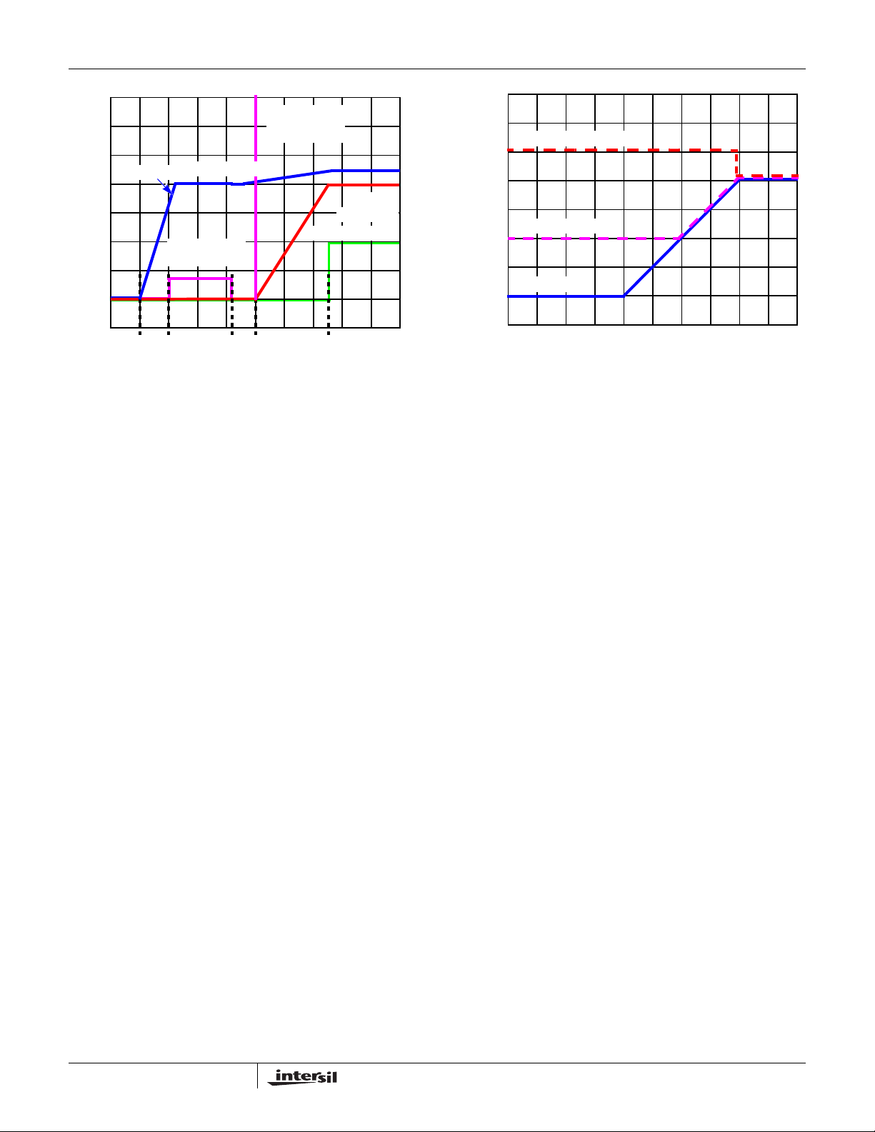
Figure 2 shows a typical power-up sequence in more detail.
The initialization starts at t0, when either V
V
, or the COMP/EN pin is released (after POR). The
POR
COMP/EN will be pulled up by an internal 20µA current
source, but the timing will not begin until the COMP/EN
exceeds the V
ENABLE
trip point (at t1). The external
capacitance of the disabling device, as well as the
compensation capacitors, will determine how quickly the
20µA current source will charge the COMP/EN pin. With
typical values, it should add a small delay compared to the
soft-start times. The COMP/EN will continue to ramp to ~1V.
trip point.
OCP
VCC (2V/DIV)
V
OUT
rises above
CC
(1V/DIV)
6
FN6538.2
December 2, 2008
Page 7
.
GND>
GND>
GND>
GND>
COMP/EN (0.25V/DIV)
0.7V
LGATE/OCSET
0.25V/DIV
ISL6341, ISL6341A, ISL6341B, ISL6341C
LGATE
STARTS
SWITCHING
PGOOD (2V/DIV)
V
OUT
(0.25V/DIV)
GND>GND>
GND>
V
OVERCHARGED
OUT
V
PRE-BIASED
OUT
V
NORMAL
OUT
t0 t1 t2 t3 t4
4.0ms
FIGURE 2. LGATE/OCSET AND SOFT-START OPERATION
0.8ms 4.0ms
From t1, there is a nominal 4ms delay, which allows the VCC
pin to rise. At the same time, the LGATE/OCSET pin is
initialized by disabling the LGATE driver and drawing I
(nominal 10µA) through R
. This sets up a voltage that
OCSET
OCSET
will represent the OCSET trip point for the OCP sa m ple and
hold operation. The sample and hold uses a digital counter and
DAC (to save the voltage so the stored value does not degrade)
for as long as the V
is above V
CC
. See “Overcurrent
POR
Protection (OCP)” on page 8 for more details on the equations
and variables. Upon the completion of sample and hold at t2,
the soft-start operation is initiated (around 0.8ms delay to t3),
and then around 4ms for the output voltage to ramp up (0% to
100%) between t3 and t4. The PGOOD output is allowed to go
high at t4 if VOS (and thus V
) is within the PGOOD
OUT
window.
Soft-Start and Pre-Biased Outputs
Functionally, the sof t-start internally ramps the reference on the
non-inverting terminal of the error amp from zero to 0.8V in a
nominal 4ms. The output voltage will thus follow the ramp, from
zero to final value, in the same 4ms. The ramp is created
digitally , so there will be small discrete steps. There is no simple
way to change this ramp rate externally, as it is fixed by the
300kHz (or 600kHz) switching frequency (and the ramp and
delay time is the same for both frequencies).
After an initialization period (t2 to t3), the error amplifier
(COMP/EN pin) is enabled, and begins to regulate the
converter’s output voltage during soft-start. The oscillator’s
triangular waveform is compared to the ramping error amplifier
voltage. This generates PHASE pulses of increasing width that
charge the output capacitors. When the internally generated
soft-start voltage exceeds the reference voltage (0.8V), the
soft-start is complete, and the output should be in regulation at
the expected voltage. This method provides a rapid and
controlled output voltage rise; there is no large in-rush current
charging the output capacitors. The entire start-up sequence
from POR typically takes 9ms; 5ms for the delay and OCP
sample, and 4ms for the soft-start ramp.
t0 t1 t2
FIGURE 3. SOFT-START WITH PRE-BIAS
Figure 3 shows the normal V
curve in blue; initialization
OUT
begins at t0, and the output ramps between t1 and t2. If the
output is pre-biased to a voltage less than the expected
value (as shown by the magenta curve), the ISL6341x will
detect that condition. Neither MOSFET will turn-on until the
soft-start ramp voltage exceeds the output; V
OUT
starts
seamlessly ramping from there.
There is a restriction for the pre-bias case; if the pre-biased
V
is greater than VGD, then the boot cap may get
OUT
discharged, and will not be able to restart. For example, if
V
= 12V , V
IN
= 8V and prebiased to 6V, and VGD is only
OUT
5V, then the voltage left on the boot cap (to UGATE) will not
be able to turn on the upper FET. The simple solution here is
to use the 12V for V
diode - Vth upper FET > V
. The guideline is to make VGD -
GD
to prevent this condition.
OUT
If the output is pre-biased to a voltage above the expected
value (as in the red curve), neither MOSFET will turn-on until
the end of the soft-start, at which time it will pull the output
voltage quickly down to the final value. Any resistive load
connected to the output will help pull-down the voltage (at
the RC rate of the R of the load and the C of the output
capacitance).
One exception to the overcharged case is if the pre-bias is
high enough to trip OV protection (>1V on VOS); then
LGATE will pulse to try to pull V
latched in this mode until V
If the V
to the upper MOSFET drain (or the VGD voltage to
IN
CC
lower. The IC will remain
OUT
power is toggled.
the boot diode) is from a different supply that comes up after
V
, the soft-start would start its cycle, but with no output
CC
voltage ramp. Once the undervoltage protection is enabled
(at the end of the soft-start ramp), the output will latch off.
Therefore, for normal operation, V
enough before or with V
. If this is not possible, then the
CC
(and VGD) must be high
IN
alternative is add sequencing logic to the COMP/EN pin to
delay the soft-start until the V
(and VGD) supply is ready
IN
(see “Input Voltage Considerations” on page 12).
7
FN6538.2
December 2, 2008
Page 8
ISL6341, ISL6341A, ISL6341B, ISL6341C
If the IC is disabled after soft-start (by pulling COMP/EN pin
low), and then enabled (by releasing the COMP/EN pin),
then the full initialization (including a new OCP sample) will
take place.
I
INDUCTOR
(10A/DIV)
If the output is shorted to GND during soft-start, the OCP will
handle it, as described in the next section.
Overcurrent Protection (OCP)
The overcurrent function protects the converter from a shorted
output by using the lower MOSFET’s ON-resistance, r
to monitor the current. A resistor (R
OCSET
) programs the
overcurrent trip level (see “T ypical Application” on page 3).
This method enhances the converter’s efficiency and reduces
cost by eliminating a current sensing resistor.
Following POR and release of COMP/EN, the ISL6341x
initiates the Overcurrent Protection sample and hold
operation. The LGATE driver is disabled to allow an internal
10µA current source to develop a voltage across R
The ISL6341x samples this voltage (which is referenced to
the GND pin) at the LGATE/OCSET pin, and holds it in a
counter and DAC combination. This sampled voltage is held
internally as the Overcurrent Set Point, for as long as power
is applied, or until a new sample is taken after coming out of
a COMP/EN shut-down.
The actual monitoring of the lower MOSFET’s ON-resistance
starts 200ns (nominal) after the edge of the internal PWM logic
signal (that creates the rising external LGATE signal). This is
done to allow the gate transition noise and ringing on the
PHASE pin to settle out before monitoring. The monitoring
ends when the internal PWM edge (and thus LGATE) goes low.
The OCP can be detected anywhere within the above window.
To allow sufficient time to detect OCP, the regulator will limit
the maximum UGATE duty cycle to ~85% at 300kHz (~75%
at 600kHz); there will always be an LGATE pulse of at least
300ns. This minimum width will also act as a boot-refresh
function. If the boot capacitor loses any charge while UGATE
is high, it will be refreshed each cycle while LGATE is high.
DS(ON)
OCSET
.
OC
1/2 OC
0A>
LGATE (12V/DIV)
,
GND>
UGATE (24V/DIV)
GND>
FIGURE 4. OCP TIMING (ISL6341, ISL6341B)
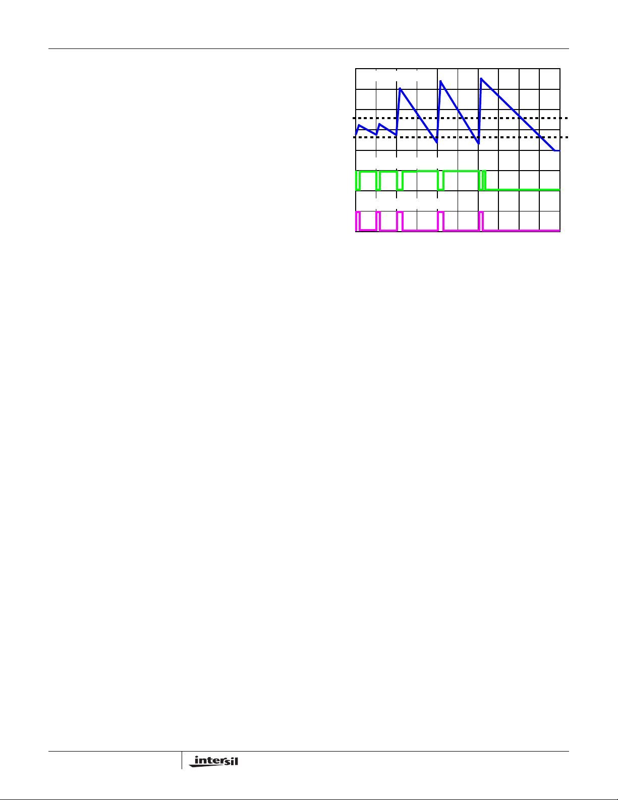
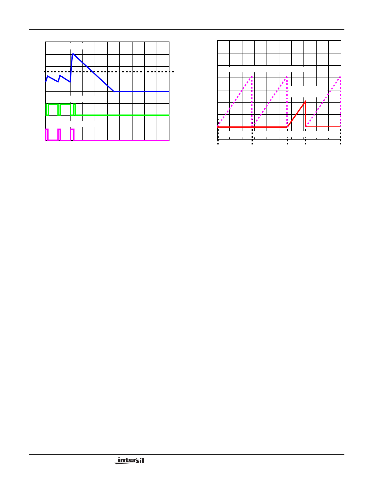
Figure 4 shows a typical waveform for the ISL6341,
ISL6341B, where the normal inductor current is around 10A,
and the OCP trip is 16A. This is just an illustration; the actual
shape of the waveforms depends on the component values,
as well as the characteristics of the load and the short. On the
third trip, the gate drivers stop switching, and the current goes
to zero. To recover from this latched off conditio n, the use r
must toggle V
(power-down and power-up) for a new POR,
CC
or toggle COMP/EN pin to restart (either includes initialization
and soft-start).
As the output inductor current rises and falls, the output
voltage is also affected. Note that in extreme cases during
the three consecutive trips, the UV may actually trip before
the OCP. The IC provides protection in either case, but
perhaps not quite at the programmed current. An OCP trip
can be reset by toggling either POR or COMP/EN, but a UV
trip is only reset by toggling POR. See Table 2 for the
protection summary.
Starting up into a shorted load will be handled the same way;
but the waveforms may look different, since the output is not
yet at its final value. OCP is always enabled during soft-start
(UV is not); it will need the three consecutive trips to latch off.
The ISL6341x share most of the detection circuitry; the main
difference among them is what happens after detection.
ISL6341, ISL6341B
When overcurrent is detected (while LGA TE is high), th e logic
will disable UGATE, and leave LGATE high until the current
drops to 1/2 of its programmed OCP value. This may take
several clock cycles, and it keeps the current from building up
too high. Once the current is low enough, UGATE will go high
on the next PWM cycle, and OCP will be monitored when
LGA TE goes high. If OCP trips a 2nd time , i t will again wa it
until the current drops. If it trips for the 3rd time, it will latch of f
the output (LGA TE and UGA TE low). If there is no OCP trip on
one of the retries, then the trip-counter resets to zero, and
three new consecutive cycles are required to latch off.
8
ISL6341A, ISL6341C
Figure 5 shows the same conditions for the ISL6341A,
ISL6341C. For this version, when overcurrent is first
detected (while LGATE is high), the logic will shut off the
output (LGATE and UGATE both go low), and the current
goes to zero.
It will then go into a “hiccup” mode of infinite retries. After two
dummy soft-start time-outs, a real soft-start will begin. If the
short is still there, it will trip during the soft-start ramp, and
will start another retry cycle. Once the short is removed, the
next real soft-start will be successful, and normal operation
can continue.
FN6538.2
December 2, 2008
Page 9
ISL6341, ISL6341A, ISL6341B, ISL6341C
.
I
INDUCTOR
(10A/DIV)
OC
0A>
LGATE (12V/DIV)
GND>
UGATE (24V/DIV)
GND>
FIGURE 5. OCP TIMING (ISL6341A, ISL6341C)
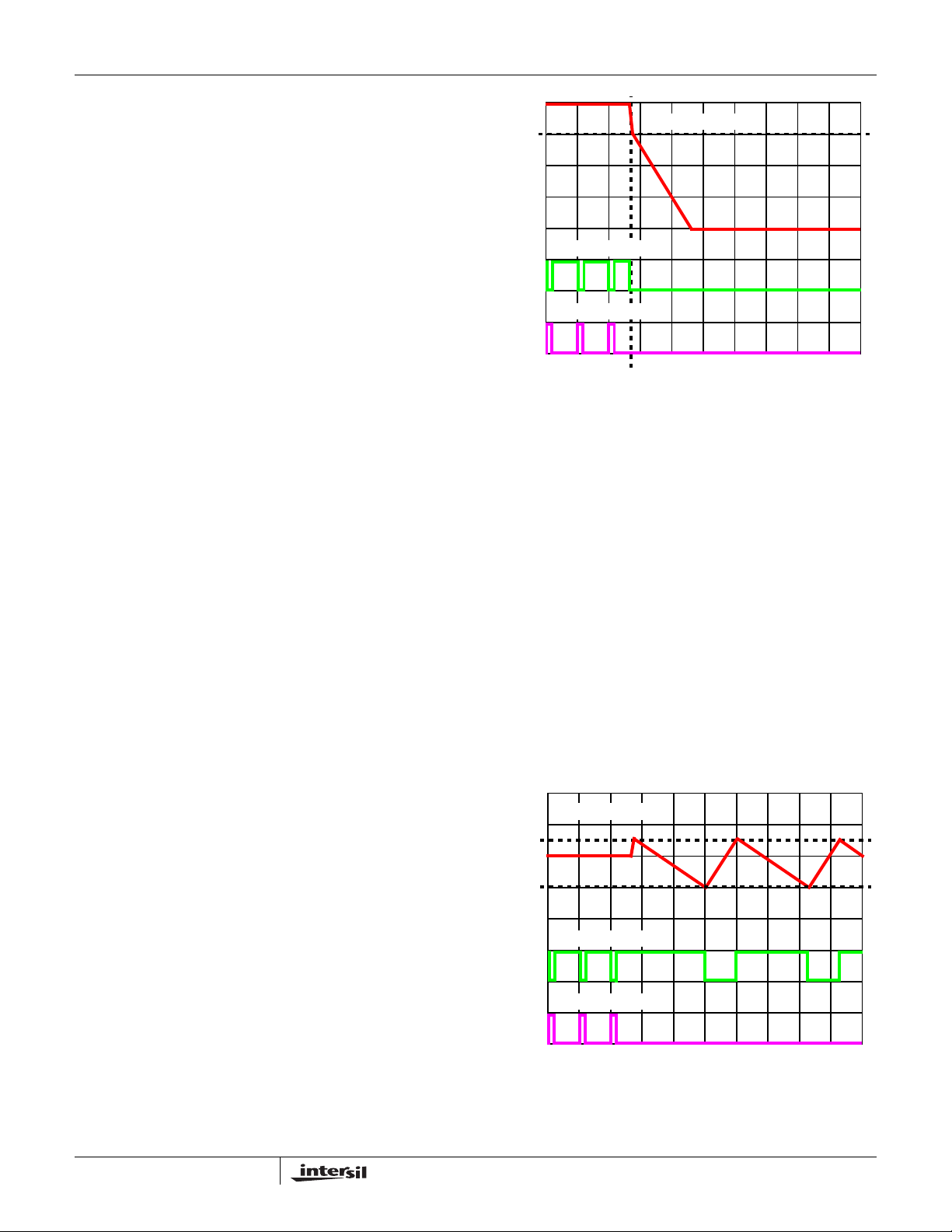
Figure 6 shows the ISL6341A, ISL6341C output response
during a retry of an output shorted to GND. At time t0, the
output has been turned off, due to sensing an overcurrent
condition. There are two internal soft-start delay cycles (t1
and t2) to allow the MOSFETs to cool down, to keep the
average power dissipation in retry at an acceptable level. At
time t2, the output starts a normal soft-start cycle, and the
output tries to ramp. If the short is still applied, and the
current reaches the OCSET trip point any time during
soft-start ramp period, the output will shut off and return to
time t0 for another delay cycle. The retry period is thus two
dummy soft-start cycles plus one variable one, which
depends on how long it takes to trip the sensor each time.
Figure 6 shows an example where the output gets about
half-way up before shutting down; therefore, the retry (or
hiccup) time will be around 12ms. The minimum should be
nominally 9.6ms and the maximum 14.4ms. If the short
condition is finally removed, the output should ramp up
normally on the next t2 cycle.
Starting up into a shorted load looks the same as a retry into
that same shorted load. In both cases, OCP is always
enabled during soft-start; once it trips, it will go into retry
(hiccup) mode. The retry cycle will always have two dummy
time-outs, plus whatever fraction of the real soft-start time
passes before the detection and shut-off; at that point, the
logic immediately starts a new two dummy cycle time-out.
Both OCP and UVP protect against shorts to GND, but the
responses (and recovery from) are different, as shown in
Table 2. For some combinations of output components and
shorting method, it may be difficult to predict which
protection will trip first (output voltage going too low, or
current going too high). The ISL6341C removes that
uncertainty by disabling the UVP, and relying only on the
OCP. Note that for the other 3 versions, if OCP trips first, it
locks out the UVP from also tripping, so that only the OCP
response (and recovery) are active.
INTERNAL SOFT-START RAMP DELAYS
V
OUT
(0.5V/DIV)
GND>
4.8ms4.8ms 0ms TO 4.8ms
t0
FIGURE 6. OCP RETRY OPERATION (ISL6341A, ISL6341C)
t1
t2
4.8ms
t0
OVERCURRENT EQUATIONS
For all the ISL6341x, versions, the overcurrent function will
trip at a peak inductor current (I
determined by
PEAK)
Equation 1:
I
PEAK
where I
OCSETxROCSET
-------------------------------------------------=
r
DS ON()
is the internal OCSET current source (10µA
OCSET
(EQ. 1)
I
typical). The OC trip point varies in a system mainly due to
the MOSFET’s r
variations (over process, current and
DS(ON)
temperature). To avoid overcurrent tripping in the normal
operating load range, find the R
OCSET
resistor from
Equation 1 with:
1. The maximum r
at the highest junction
DS(ON)
temperature.
2. The minimum I
from the “Electrical Specification
OCSET
Tabl e” on page 5.
ΔI()
3. Determine I
PEAK
I
for
PEAKIOUT MAX()
where ΔI is the output inductor ripple current.
----------
+>
,
2
For an equation for the ripple current see “Output Inductor
Selection” on page 15.
The range of allowable voltages detected (I
OCSET*ROCSET
is 0mV to 550mV; but the practical range for typical
MOSFETs is smaller. If the voltage drop across R
OCSET
is
set too low (< ~20mV), that can cause almost contin u ous
OCP tripping. It would also be very sensitive to system noise
and in-rush current spikes, so it should be avoided. The
maximum setting is 550mV, but most of the recommended
MOSFETs for the ISL6341x are not expected to handle the
power of the maximum trip point.
There is no way to disable the OCP, but setting it above the
maximum value (>600mV) will come close; for most cases, it
should be high enough (compared to the normal expected
range) to appear disabled. No resistor at all could give the
clamped maximum value (unless the loading on the LGATE
prevents charging the node fully). But there is no low-voltage
clamp on LGATE, so it could rise to over 3V and turn-on for
)
9
FN6538.2
December 2, 2008
Page 10
ISL6341, ISL6341A, ISL6341B, ISL6341C
4ms during the sampling; that could discharge a pre-biased
output. Therefore, to avoid that case, but still come close to
disabling OCP, a resistor (>60kΩ) is recommended.
Note that conditions during power-up may look different than
normal operation. For example, during power-up in a 12V
system, the IC starts operation just above 4V; if the supply
ramp is slow, the soft-start ramp might be over well before
12V is reached. So with lower gate drive voltages, the
r
effectively lowering the OCP trip. In addition, the ripple
current will likely be different at lower input voltage.
Another factor is the digital nature of the soft-start ramp. On
each discrete voltage step, there is in effect a small load
transient and a current spike to charge the output capacitors.
The height of the current spike is not controlled; it is affected
by the step size of the output, the value of the output
capacitors, as well as the IC error amp compensation. So it
is possible to trip the overcurrent with in-rush current, in
addition to the normal load and ripple considerations.
OCP is always enabled during soft-start, so there is
protection starting up into a shorted load.
Undervoltage Protection
The output is protected against undervoltage conditions by
monitoring the VOS pin. An external resistor divider (similar
ratio to the one on the FB pin) makes the voltage equal the
0.8V internal reference under normal operation. If the output
goes too low (25% below 0.8V = 0.6V nominal on VOS), the
output will latch off, with UGAT E and LGA TE both forced low .
This requires toggling V
(toggling COMP/EN will NOT restart it). The UV protection is
not enabled until the end of the soft-start ramp (as shown in
Figure 2).
Figure 7 shows a case where V
down to the 75% point; both gate drivers stop switching, and
the V
load, at a rate determine by the conditions, and the output
components.
The ISL6341C version does not have UVP; it relies on the
OCP for shorted loads. The PGOOD UV comparator is
separate, and is still active.
of the MOSFETs will be higher during power-up,
DS(ON)
(power-down and up) to restart
CC
(and thus VOS) is pulled
OUT
is pulled low by the disturbance, as well as the
OUT
V
(0.25V/DIV)
75%
GND>
LGATE (12V/DIV)
GND>
UGATE (24V/DIV)
GND>
FIGURE 7. UNDERVOLTAGE PROTECTION
OUT
Overvoltage Protection
The output is protected against overvoltage conditions by
monitoring the VOS pin, similar to undervoltage. If the output
goes too high (25% above 0.8V = 1.0V nominal on VOS), the
output will latch off. As shown in Figure 8, UGATE will be
forced low, but LGATE will be forced high (to try to pull-down
the output) until the output drops to 1/2 of the normal voltage
(50% of 0.8V = 0.4V nominal on VOS). The LGATE will then
shut off, but will keep turning back on whenever the output
goes too high again.
Overvoltage latch-off requires togglin g V
up) to restart (toggling COMP/EN will NOT restart it). The OV
protection is not enabled until the rising V
exceeded. The OV protection is active during soft-st art at the
fixed 25% above the final expected voltage. The OVP is not
gated off by tripping OCP (but the UVP is gated off if OCP
trips first).
If the VOS pin is disconnected, a small bias current on-chip
will force an overvoltage condition.
V
(0.5V/DIV)
OUT
125%
50%
(power-down and
CC
POR trip point is
CC
10
GND>
GND>
GND>
LGATE (12V/DIV)
UGATE (24V/DIV)
FIGURE 8. OVERVOLTAGE PROTECTION
FN6538.2
December 2, 2008
Page 11
ISL6341, ISL6341A, ISL6341B, ISL6341C
PGOOD
The PGOOD function output monitors the output voltage
using the same VOS pin and resistor divider of the
undervoltage and overvoltage protection, but wi th sep a rate
comparators for each. The rising OV trip point (10% above
0.8V = 0.88V nominal on VOS) and the falling UV trip point
(10% below 0.8V = 0.72V nominal on VOS) will trip sooner
than the protection, in order to give an early warning to a
possible problem. The response time of the comparators
should be less than 1µs; the separate VOS input is not slowed
down by the compensation on the FB pin. It is NOT
recommended to connect the VOS pin to the FB pin, in order
to share the resistor divider. If the VOS pin is accident al ly
disconnected, a small bias current on-chip will force an
overvoltage condition.
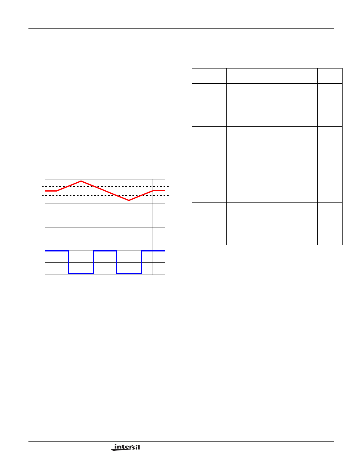
Figure 9 shows how the PGOOD output responds to a ramp
that trips in each direction (without reaching either protection
trip point at ±25%); PGOOD is valid (high) as long as V
(and thus VOS) is within the ±10% window.
110%
90%
V
(0.25V/DIV)
OUT
GND>
PGOOD (2V/DIV)
GND>
FIGURE 9. PGOOD UNDERVOLTAGE AND OVERVOLTAGE
The PGOOD output is an open-drain pull-down NMOS
device; it can deliver 4.0mA of sink current at 0.3V when
power is NOT GOOD. A pull-up resistor to an external supply
voltage sets the high level voltage when power is GOOD. The
supply should be ≤6.0V, and is usually the one that powers
the logic monitoring the PGOOD output. If PGOOD function is
not used, the PGOOD pin can be left floating.
The PGOOD pin will be held low once V
is above the rising
CC
POR trip point, and during soft-start (but if the PGOOD supply
is up before or with V
, it may be pulled high initially until the
CC
logic has enough voltage to turn on the output). Once the
soft-start ramp is done (V
, VOS and FB should each be at
OUT
100% of their final value), the PGOOD pin will be allowed to
go high, if the output voltage is within the expected window.
There is no additional delay after soft-start is done.
Note that the overcurrent protection does directly affect the
PGOOD output, before the output voltage monitoring would
sense when V
drops 10%. The overvoltage and
OUT
undervoltage protection circuits don’t directly effect PGOOD,
OUT
but since the PGOOD UV and OV windows are tighter, the
PGOOD output should already be low by the time either
protection is tripped.
TABLE 2. PROTECTION SUMMARY
PROTECTION ACTION TAKEN
OCP
ISL6341
ISL6341B
OCP
ISL6341A
ISL6341C
UVP
(-25%)
OVP
(+25%)
PGOOD
(UV; -10%)
PGOOD
(OV; +10%)
PGOOD
(OCP)
V
latches off;
OUT
LGATE and UGATE low.
Infinite retries; wait ~10ms,
and try a new Soft-Start ramp.
ISL6341C has UVP disabled
V
latches off;
OUT
LGATE and UGATE low.
ISL6341C has UVP disabled
V
latches off;
OUT
UGATE low;
LGATE goes low and high to
keep V
125% of nominal.
VOS pin open will trigger OV.
PGOOD goes low if VOS is
10% too low.
PGOOD goes low if VOS is
10% too high.
PGOOD goes low if OCP trips after SS
within 50% and
OUT
ENABLED
AFTER
POR or
COMP/EN
POR or
COMP/EN
after SS
ramp
POR POR
after SS
ramp
after SS
ramp
ramp
RESET
BY
POR or
COMP/EN
Not
Applicable
POR
POR or
COMP/EN
POR or
COMP/EN
POR or
COMP/EN
or good
SS ramp
Switching Frequency
The switching frequency is a fixed 300kHz for the ISL6341,
ISL6341C and 600kHz for the ISL6341A, ISL6341B. It
cannot be adjusted externally, and the various soft-start
delays and ramps are fixed at the same times for either
frequency.
Output Voltage Selection
The output voltage can be programmed to any level between
the 0.8V internal reference, up to the V
85% duty cycle restriction for the ISL6341, ISL6341C (75%
for the ISL6341A, ISL6341B). Additional duty cycle margin
due to the r
drop across the upper FET at maximum
DS(ON)
load needs to be factored in as well.
An external resistor divider is used to scale the output
voltage relative to the internal reference voltage, and feed it
back to the inverting input of the error amp. See the “Typical
Application” schematic on page 3 for more detail; R
upper resistor; R
OFFSET
(shortened to RO below) is the
lower one. The recommended value for R
(±1% for accuracy) and then R
to Equation 2. Since R
S
OFFSET
is part of the compensation circuit
(see “Feedback Compensation” on page 13), it is often
easier to change R
OFFSET
to change the output voltage;
that way the compensation calculations do not need to be
supply, with the
IN
is the
S
is 1kΩ to 5kΩ
S
is chosen according
11
FN6538.2
December 2, 2008
Page 12
ISL6341, ISL6341A, ISL6341B, ISL6341C
repeated. If V
= 0.8V, then R
OUT
OFFSET
can be left open.
Output voltages less than 0.8V are not available.
V
R
OUT
O
----------------------------------
=
V
0.8V
RS0.8V•
OUT
---------------------------
•=
R
0.8V–
O
(EQ. 2)
+()
R
SRO
The VOS pin is expected to see the same ratio for its resistor
divider; R
(±1% for accuracy) range. To simplify the BOM, R
should match RS, and R
should also be chosen in the 1kΩ to 5kΩ
VOS1
should match R
VOS2
VOS1
OFFSET
.
If margining (or similar programmability) is added externally
(using a switch to change the effective lower resistor value),
the same method may be needed on the VOS pin resistor
divider. If the new VOUT (FB) is s hi fted too much compared
to the VOS trip, then PGOOD or UV/OV will be more likely to
trip in one direction (and less likely in the other).
Input Voltage Considerations
The “Typical Application” diagram on page 3 shows a
standard configuration where V
includes the standard 5V (±10%) or 12V (±20%) power
supply ranges. The gate drivers use the V
LGA TE, and V
(also 5V to 12V) for BOOT/UGATE. There
GD
is an internal 5V regulator for bias.
The V
as V
to the upper MOSFET can share the same supply
IN
, but can also run off a separate supply or other
CC
sources, such as outputs of other regulators. If V
up first, and the V
or VGD are not present by the time the
IN
initialization is done, then undervoltage will trip at the end of
soft-start (and will not recover without toggling V
COMP/EN will not restart it). Therefore, either the supplies
must be turned on in the proper order (together, or V
or the COMP/EN pin should be used to disable V
supplies are ready.
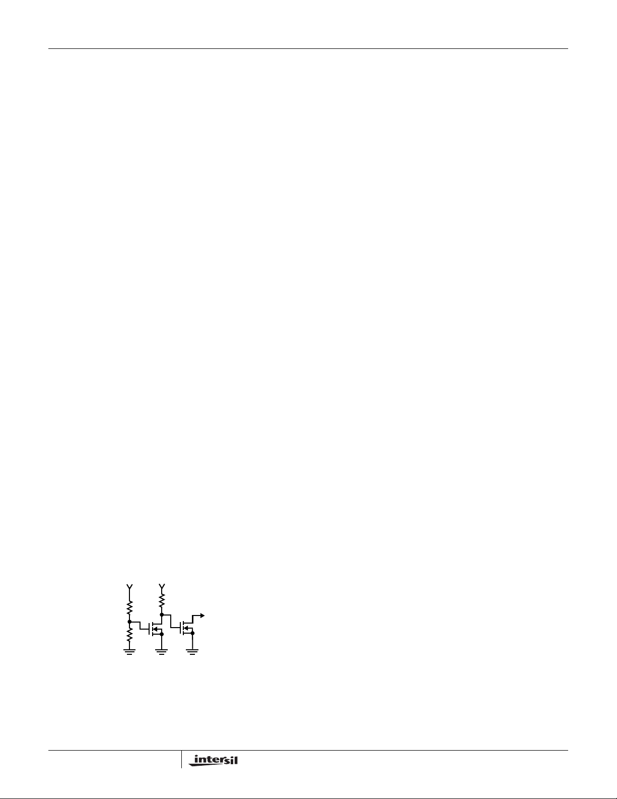
Figure 10 shows a simple sequencer for this situation. If V
powers up first, Q
Q
on, keeping the ISL6341x in shut-down. When VIN turns
2
on, the resistor divider R
on, which will turn off Q
will be off and R3 pulling to VCC will turn
1
and R2 determines when Q1 turns
1
, and release the shut-down.
2
V
IN
R
R
1
R
2
FIGURE 10. SEQUENCER CIRCUIT
3
Q
is 5V to 12V, which
CC
V
CC
TO COMP/EN
Q
1
2
voltage for
CC
CC
OUT
powers
CC
; toggling
last),
CC
until all
CC
If V
powers up first, Q1 will be on, turning Q2 off; so the
IN
ISL6341x will start-up as soon as V
V
ENABLE
trip point is 0.7V nominal, so a wide variety of
NFET’s or NPN’s or even some logic IC’s can be used as Q
or Q
. But Q2 should pull down hard when on, and must be
2
comes up. The
CC
1
low leakage when off (open-drain or open-collector) so as
not to interfere with the COMP output. The V
(or Vbe) of Q2
th
should be reviewed over process and temperature variations
to insure that it will work properly under all conditions. Q
2
should be placed near the COMP/EN pin.
The V
the 0.8V reference). It can be as high as 20V (for V
below V
some restrictions for running high V
range can be as low as ~1.5V (for V
IN
, limited by the maximum duty cycle). There are
IN
IN
OUT
voltage.
as low as
just
OUT
The first consideration for high VIN is the maximum BOOT
voltage of 36V . The V
(as seen on PHASE) plus VGD (boot
IN
voltage - minus the diode drop), plus any ringing (or other
transients) on the BOOT pin must be less than 36V. If V
20V, that limits V
plus ringing to 16V.
GD
IN
is
The second consideration is the maximum voltage ratings
for V
V
14.4V, then both V
separately. They can be derived from V
and BOOT-PHASE (for VGD); both are set at 15V. If
CC
is above the maximum operating range for VCC of
IN
and VGD need to be supplied
CC
(using a linear
IN
regulator or equivalent), or they can be independent. In
either case, they must satisfy the power supply sequencing
requirements noted earlier (either power-up in the proper
order, or use a sequencer to disable the output until they are
all ready).
The third consideration for high V
is duty cycle. Very low
IN
duty cycles (such as 20V in to 1.0V out, for 5% duty cycle)
require component selection compatible with that choice
(such as low r
lower MOSFET, a good LC output
DS(ON)
filter, and compensation values to match). At the other
extreme (for example, 20V in to 12V out), the upper
MOSFET needs to be lower r
. There is also the
DS(ON)
maximum duty cycle restriction. In all cases, the input and
output capacitors and both MOSFETs must be rated for the
voltages present.
Application Guidelines
Layout Considerations
As in any high frequency switching converter, layout is very
important. Switching current from one power device to another
can generate voltage transients across the impedances of the
interconnecting bond wires and circuit traces. These
interconnecting impedances should be minimized by using
wide, short printed circuit traces. The critical components
should be located as close together as possible, using ground
plane construction or single point grounding.
12
FN6538.2
December 2, 2008
Page 13
ISL6341, ISL6341A, ISL6341B, ISL6341C
.
V
ISL6341x
UGATE
PHASE
LGATE/OCSET
IN
Q
1
Q
2
RETURN
L
O
V
OUT
C
IN
C
O
LOAD
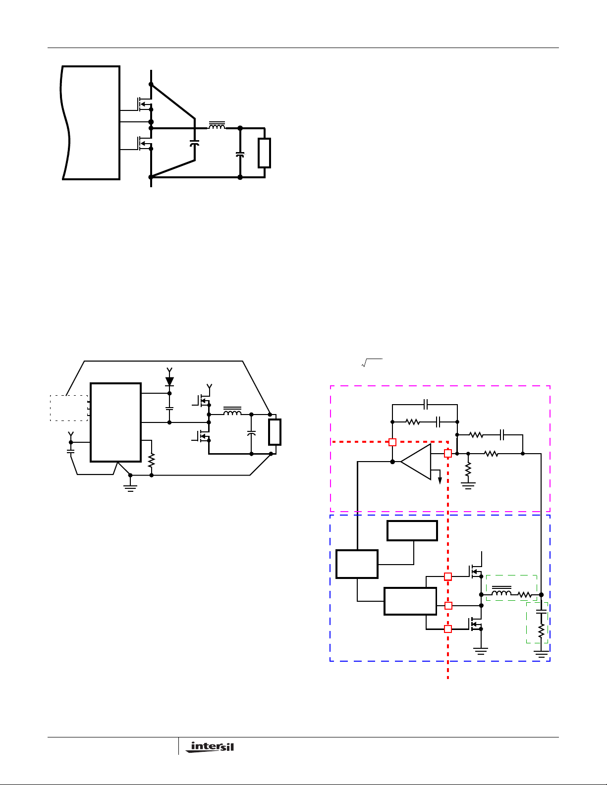
FIGURE 11. PRINTED CIRCUIT BOARD POWER AND
GROUND PLANES OR ISLANDS
Figure 11 shows the critical power components of the
converter. To minimize the voltage overshoot, the
interconnecting wires indicated by heavy lines should be part of
a ground or power plane in a printed circuit board. The
components shown should be located as close together as
possible. Please note that the capacitors C
and CO may each
IN
represent numerous physical capacitors. For best results,
loca te t he ISL6341x wi thi n 1 inch of the MOSFETs, Q
and Q2.
1
The circuit traces for the MOSFET gate and source
connections from the ISL6341x must be sized to handle up to
2A peak current.
+V
GD
+V
Q
Q
IN
L
1
O
V
OUT
C
O
2
LOAD
V
OUT
VOS
COMP/EN
+V
CC
C
VCC
FB
VCC
ISL6341x
GND
BOOT
C
BOOT
PHASE
LGATE/OCSET
R
OCSET
FIGURE 12. PRINTED CIRCUIT BOARD SMALL SIGNAL
LAYOUT GUIDELINES
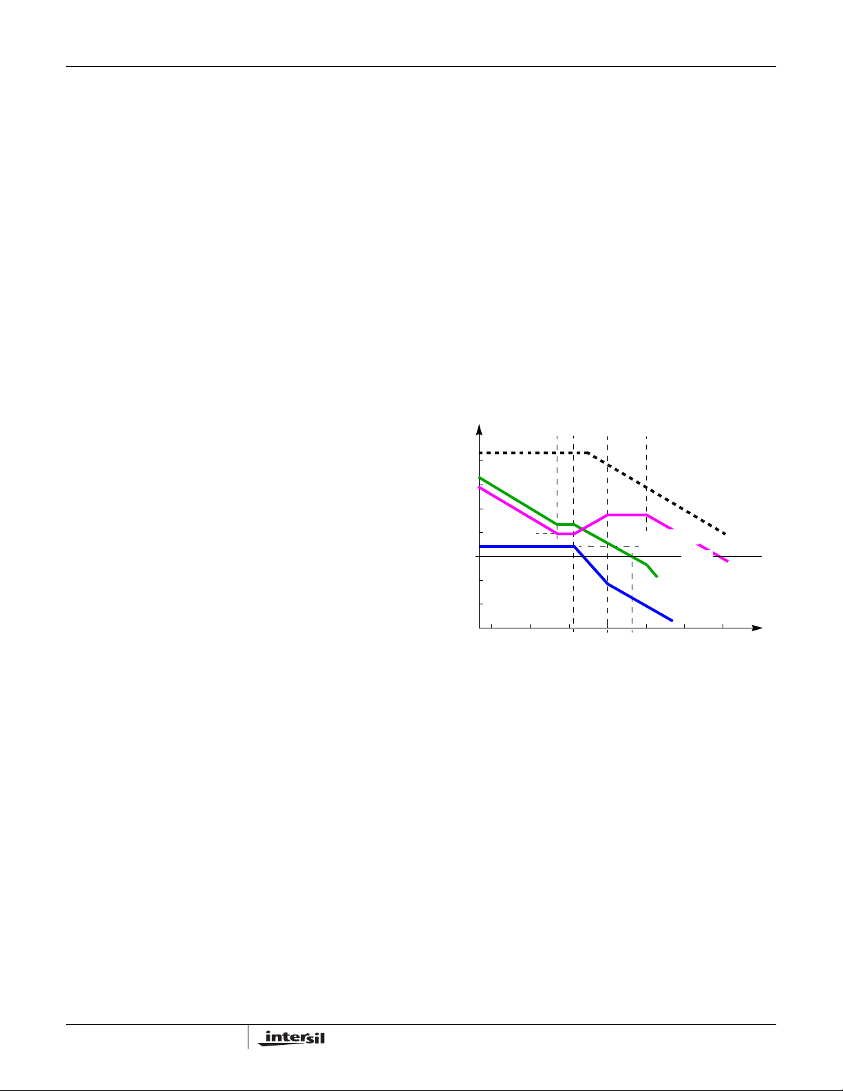
Feedback Compensation
This section highlights the design consideration for a
voltage-mode controller requiring external compensation. To
address a broad range of applications, a type-3 feedback
network is recommended, as shown in the top part of
Figure 13.
Figure 13 also highlights the voltage-mode control loop for a
synchronous-rectified buck converter, applicable to the
ISL6341x circuit. The output voltage (V
the reference voltage, V
. The error amplifier output
REF
(COMP pin voltage) is compared with the oscillator (OSC)
modified sawtooth wave to provid e a pu l se-w i dth modulated
wave with an amplitude of V
at the PHASE node. The
IN
PWM wave is smoothed by the output filter (L and C). The
output filter capacitor bank’s equivalent series resistance is
represented by the series resistor E.
The modulator transfer function is the small-signal transfer
function of V
OUT/VCOMP
gain, given by d
MAXVIN/VOSC
. This function is dominated by a DC
, and shaped by the output
filter, with a double pole break frequen cy at F
F
. For the purpose of this analysis, L and D represent the
CE
channel inductance and its DCR, while C and E represent the
total output capacitance and its eq uivalent series resist ance.
1
---------------------------
F
LC
=
2π LC⋅⋅
COMP
R2
E/A
F
C2
-
+
VREF
CE
C1
------------------------
=
2π CE⋅⋅
FB
OUT
1
R3
R1
Ro
) is regulated to
and a zero at
LC
(EQ. 3)
C3
Figure 12 shows the circuit traces that require additional
layout consideration. Use single point and ground plane
construction for the circuits shown. Provide local V
CC
decoupling between VCC and GND pins. Locate the
capacitor , C
PHASE pins. Locate the resistor, R
as close as practical to the BOOT and
BOOT
OSCET
close to the
LGATE/OCSET pin because the internal current source is
only 10µA. Minimize any leakage current paths on the
COMP/EN pin. All components used for feedback
compensation and VOS resistor divider (inside the dotted
box) should be located as close to the IC as practical. Near
the load, pick a point V
that will be the regulation center;
OUT
run a single unloaded narrow trace from there to the
compensation components. The same trace can also be
used for VOS divider.
13
OSCILLATOR
V
IN
V
PWM
CIRCUIT
OSC
HALF-BRIDGE
DRIVE
ISL6341x
UGATE
PHASE
LGATE
EXTERNAL CIRCUIT
L
FIGURE 13. VOLTAGE-MODE BUCK CONVERTER
COMPENSATION DESIGN
V
OUT
D
C
E
FN6538.2
December 2, 2008
Page 14
ISL6341, ISL6341A, ISL6341B, ISL6341C
The compensation network consists of the error amplifier
(internal to the ISL6341x) and the external R
to R3, C1 to C3
1
components. The goal of the compensation network is to
provide a closed loop transfer function with high 0dB crossing
frequency (F
; typically 0.1 to 0.3 of fSW) and adequate phase
0
margin (better than 45°). Phase margin is the difference
between the closed loop phase at F
and 180°. The
0dB
equations that follow relate the compensation network’s poles,
zeros and gain to the components (R
C
) in Figure 13. Use the following guidelines for locating the
3
, R2, R3, C1, C2, and
1
poles and zeros of the compensation network:
4. Select a value for R
(1kΩ to 5kΩ, typically). Calculate the
1
value for R2 for desired converter bandwidth (F0). If
setting the output voltage via an offset resistor connected
to the FB pin (R
in Figure 13), the design procedure can
o
be followed as presented in Equation 4.
V
⋅⋅
OSCR1F0
---------------------------------------------
R
=
2
d
MAXVINFLC
⋅⋅
(EQ. 4)
5. Calculate C1 such that FZ1 is placed at a fraction of the FLC,
at 0.1 to 0.75 of FLC (to adjust, change the 0.5 factor to
desired number). The higher the quality factor of the output
filter and/or the higher the ratio F
, the lower the FZ1
CE/FLC
frequency (to maximize phase boost at FLC).
=
1
⋅⋅ ⋅
2π R
2
0.5 F
LC
(EQ. 5)
1
-----------------------------------------------
C
6. Calculate C2 such that FP1 is placed at FCE.
C
--------------------------------------------------------
=
C
2
2π R2C1FCE1–⋅⋅⋅
7. Calculate R
1
such that FZ2 is placed at FLC. Calculate C3
3
(EQ. 6)
such that FP2 is placed below fSW (typically, 0. 5 to 1.0
times fSW). fSW represents the switching frequency.
Change the numerical factor to reflect desired placement
of this pole. Placement of F
lower in frequency helps
P2
reduce the gain of the compensation network at high
frequency, in turn reducing the HF ripple component at
the COMP pin and minimizing resultant duty cycle jitter.
R
3
f
SW
---------- -
1–
F
LC
-----------------------------------------------
C
=
3
2π R
1
--------------------
=
R
1
0.7 f
⋅⋅ ⋅
3
SW
(EQ. 7)
It is recommended that a mathematical model be used to
plot the loop response. Check the loop gain against the error
amplifier’s open-loop gain. Verify phase margin results and
adjust as necessary. Equations 8 and 9 describe the
frequency response of the modulator (G
compensation (G
) and closed-loop response (GCL):
FB
), feedback
MOD
G
G
G
MOD
FB
CL
d
MAXVIN
----------------------------- -
f()
V
OSC
1sf() 2
---------------------------------------------------
f()
R1C2C
sf() 1
------------------------------------------------------------------------------------------------------------------------
⋅
1sf() 3
f() G
MOD
----------------------------------------------------------------------------------------
⋅=
1sf() ED+()C⋅⋅s
R1C
⋅⋅+
+()⋅⋅
1sf() 1
R3C
⋅⋅+()1sf() 2
f() GFBf()⋅=
1sf() EC⋅⋅+
2
f() LC⋅⋅++
⋅=
R3R
⋅⋅+
⎛⎞
⋅
⎜⎟
⎝⎠
C
+()3
R
⋅⋅+
⎛⎞
1C2C⋅
--------------------
⎜⎟
C2C
⎝⎠
+
1
where s f(), 2π fj⋅⋅=
⋅
(EQ. 8)
COMPENSATION BREAK FREQUENCY EQUATIONS
------------------------------
F
=
Z1
2π 2
------------------------------------------------
=
F
Z2
2π 1
GAIN
20
0
LOG
LOG
1
R1C
⋅⋅
1
R3R
+()3
⋅⋅
R
⎛⎞
2
⎜⎟
------- -
log
⎜⎟
R
1
⎝⎠
F
=
P1
C
F
Z1
F
F
F
F
P1
Z2
F
CE
LC
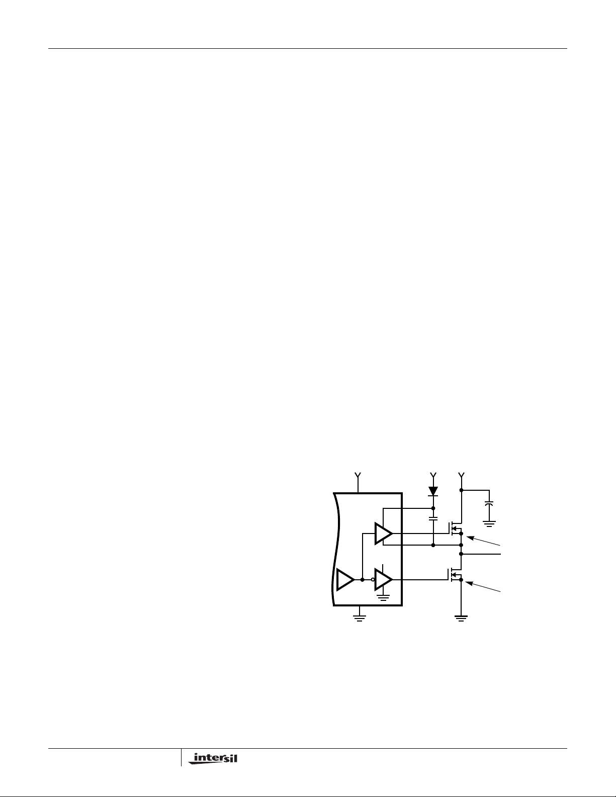
FIGURE 14. ASYMPTOTIC BODE PLOT OF CONVERTER GAIN
1
--------------------------------------------
R
1C2C⋅
2π 2
P2
--------------------
⋅⋅
C2C
+
1
1
------------------------------
=
R3C
2π 3
⋅⋅
F
P2
COMPENSATION GAIN
CLOSED LOOP GAIN
OPEN LOOP E/A GAIN
d
MAX
20
---------------------------------log
G
CL
G
F
0
V
(EQ. 9)
MODULATOR GAIN
V
⋅
IN
OSC
G
FB
MOD
FREQUENCY
Figure 14 shows an asymptotic plot of the DC/DC converter’s
gain vs frequency. The actual Modulator Gain has a high gain
peak dependent on the quality factor (Q) of the output filter,
which is not shown. Using the previous guidelines should yield
a compensation gain similar to the curve plotted. The open loop
error amplifier gain bounds the compensation gain. Check the
compensation gain at F
amplifier. The closed loop gain, G
log graph of Figure 14 by adding the modulator gain, G
dB), to the feedback compensation gain, G
against the capabilities of the error
P2
, is constructed on the log-
CL
(in dB). This is
FB
MOD
(in
equivalent to multiplying the modulator transfer function and the
compensation transfer function and then plotting the resulting
gain.
14
A stable control loop has a gain crossing with close to a
-20dB/decade slope and a phase margin greater than 45°.
Include worst case component variations when determining
phase margin. The mathematical model presented makes a
number of approximations and is generally not accurate at
frequencies approaching or exceeding half the switching
FN6538.2
December 2, 2008
Page 15

ISL6341, ISL6341A, ISL6341B, ISL6341C
frequency. When designing compensation networks, select
target crossover frequencies in the range of 10% to 30% of
the switching frequency, f
SW
.
This is just one method to calculate compensation components;
there are variations of the compensation break frequency
equations. The error amp is similar to that on other Intersil
regulators, so existing tools can be used here as well. Special
consideration is needed if the size of a ceramic output
capacitance in parallel with bulk capacitors gets too large; the
calculation needs to model them both separately (attempting to
combine two different capacitors types into one composite
component model may not work properly; a special tool may be
needed; contact your local Intersil person for assistance).
Component Selection Guidelines
Output Capacitor Selection
An output capacitor is required to filter the output and supply
the load transient current. The filtering requirements are a
function of the switching frequency and the ripple current.
The load transient requirements are a function of the slew
rate (di/dt) and the magnitude of the transient load current.
These requirements are generally met with a mix of
capacitors and careful layout.
Output Inductor Selection
The output inductor is selected to meet the output voltage
ripple requirements and minimize the converter’s response
time to the load transient. The inductor value determines the
converter’s ripple current and the ripple voltage is a function
of the ripple current. The ripple voltage and current are
approximated by Equation 10:
ΔI =
Fsw x L
- V
V
IN
Increasing the value of inductance reduces the ripple current
and voltage. However, the large inductance values reduce
the converter’s response time to a load transient.
One of the parameters limiting the converter’s response to
a load transient is the time required to change the inductor
current. Given a sufficiently fast control loop design, the
ISL6341x will pro v ide eithe r 0% or 100% duty cy c le in
response to a load transient. The response time is the time
required to slew the inductor current from an initial current
value to the transient current level. During this interval, the
difference between the inductor current and the transient
current level must be supplied by the output capacitor.
Minimizing the response time can minimize the output
capacitance required.
OUT
V
OUT
x
V
IN
ΔV
OUT
= ΔI x ESR
(EQ. 10)
Modern components and loads are capable of producing
transient load rates above 1A/ns. High frequency capacitors
initially supply the transient and slow the current load rate
seen by the bulk capacitors. The bulk filter capacitor values
are generally determined by the ESR (Effective Series
Resistance) and voltage rating requiremen t s rather th an
actual capacitance requirements.
High frequency decoupling capacitors should be placed as
close to the power pins of the load as physically possible. Be
careful not to add inductance in the circuit board wiring that
could cancel the usefulness of these low inductance
components. Consult with the ma nu facturer of the load on
specific decoupling requirements.
Use only specialized low-ESR capacitors intended for
switching-regulator applications for the bulk capacitors. The
bulk capacitor’s ESR will determine the output ripple voltage
and the initial voltage drop after a high slew-rate transi ent. An
aluminum electrolytic capacitor’s ESR value is related to the
case size with lower ESR available in larger case sizes.
However, the Equivalen t Series Induct ance (ESL) of these
capacitors increases with case size and can reduce the
usefulness of the capacitor to high slew-rate transient loading.
Unfortunately, ESL is not a specified parameter. Work with
your capacitor supplier and measure the capacitor’s
impedance with frequency to select a suitable component. In
most cases, multiple electrolytic capacitors of small case size
perform better than a single large case capacitor.
The response time to a transient is different for the
application of load and the removal of load. Equation 11
gives the approximate response time interval for application
and removal of a transient load:
L x I
t
=
RISE
where: I
TRAN
VIN - V
OUT
is the transient load current step, t
TRAN
t
FALL
response time to the application of load, and t
L x I
V
TRAN
OUT
=
FALL
RISE
is the
(EQ. 11)
is the
response time to the removal of load. The worst case
response time can be either at the application or removal of
load. Be sure to check Equation 11 at the minimum and
maximum output levels for the worst case response time.
Input Capacitor Selection
Use a mix of input bypass capacitors to control the volt age
overshoot across the MOSFETs. Use small ceramic
capacitors for high frequency decoupling and bulk capacito rs
to supply the current needed each time Q
small ceramic capacitors physically close to the MOSFETs
and between the drain of Q
and the source of Q2.
1
The important parameters for the bulk input capacitor are the
voltage rating and the RMS current rating. For reliable
operation, select the bulk capacitor with voltage and current
ratings above the maximum input voltage and largest RMS
current required by the circuit. The capacitor voltage rating
should be at least 1.25x greater than the maximum input
voltage and a voltage rating of 1.5x is a conservative
guideline. The RMS current rating requirement for the input
capacitor of a buck regulator is approximately 1/2 the DC
load current.
turns on. Place the
1
15
FN6538.2
December 2, 2008
Page 16
ISL6341, ISL6341A, ISL6341B, ISL6341C
For a through-hole design, several electrolytic capacitors may
be needed. For surface mount designs, solid tantalum
capacitors can also be used, but caution must be exercised
with regard to the capacitor surge current rating. These
capacitors must be capable of handling the surge current at
power-up. Some capacitor series available from reputable
manufacturers are surge current tested.
MOSFET Selection/Considerations
The ISL6341x requires 2 N-Channel power MOSFET s. These
should be selected based upon r
requirements, and thermal management requirements.
In high-current applications, the MOSFET power dissipation,
package selection and heatsink are the dominant design
factors. The power dissipation includes two loss components;
conduction loss and switching loss. The conduction losses are
the largest component of power dissipation for both the upper
and the lower MOSFET s. These losses are distributed between
the two MOSFETs according to duty factor. The switching
losses seen when sourcing current will be different from the
switching losses seen when sinking current. When sourcing
current, the upper MOSFET realizes most of the switching
losses. The lower switch realizes most of the switching losses
when the converter is sinking current (see Equation 12).
Equation 12 assumes linear voltage-current transitions and
does not adequately model power loss due to the reverserecovery of the upper and lower MOSFET’s body diode. The
gate-charge losses are dissipated by the ISL6341x and don't
heat the MOSFETs. However, large gate-charge increases the
switching interval, t
which increases the MOSFET switching
SW
losses. Ensure that both MOSFETs are within their maximum
junction temperature at high ambient temperature by
calculating the temperature rise according to package
thermal-resistance specifications. A separate heatsink may be
necessary depending upon MOSFET power, package type,
ambient temperature and air flow.
Losses while Sourcing Current
Io2r
= Io2 x r
× D×
DS ON()
x (1 - D)
DS(ON)
P
UPPER
P
LOWER
Losses while Sinking Current
P
P
= Io2 x r
UPPER
LOWER
Where: D is the duty cycle = V
Io2r
is the combined switch ON and OFF time, and
t
SW
is the switching frequency.
f
SW
x D
DS(ON)
× 1D–()×
DS ON()
DS(ON)
1
-- -
Io⋅ V
2
OUT
, gate supply
× t
IN
SWFS
1
-- -
× t
Io⋅ V
2
/ VIN,
IN
××+=
SWFS
(EQ. 12)
××+=
For 5V only operation, given the reduced available gate bias
voltage (5V), logic-level transistors should be used for both
N-MOSFETs. Look for r
DS(ON)
ratings at 4.5V. Caution
should be exercised with devices exhibiting very low
V
characteristics. The shoot-through protection
GS(ON)
present aboard the ISL6341x may be circumvented by these
MOSFETs if they have large parasitic impedences and/or
capacitances that would inhibit the gate of the MOSFET from
being discharged below its threshold level before the
complementary MOSFET is turned on. Also avoid MOSFET s
with excessive switching times; the circuitry is expecting
transitions to occur in under 50ns or so.
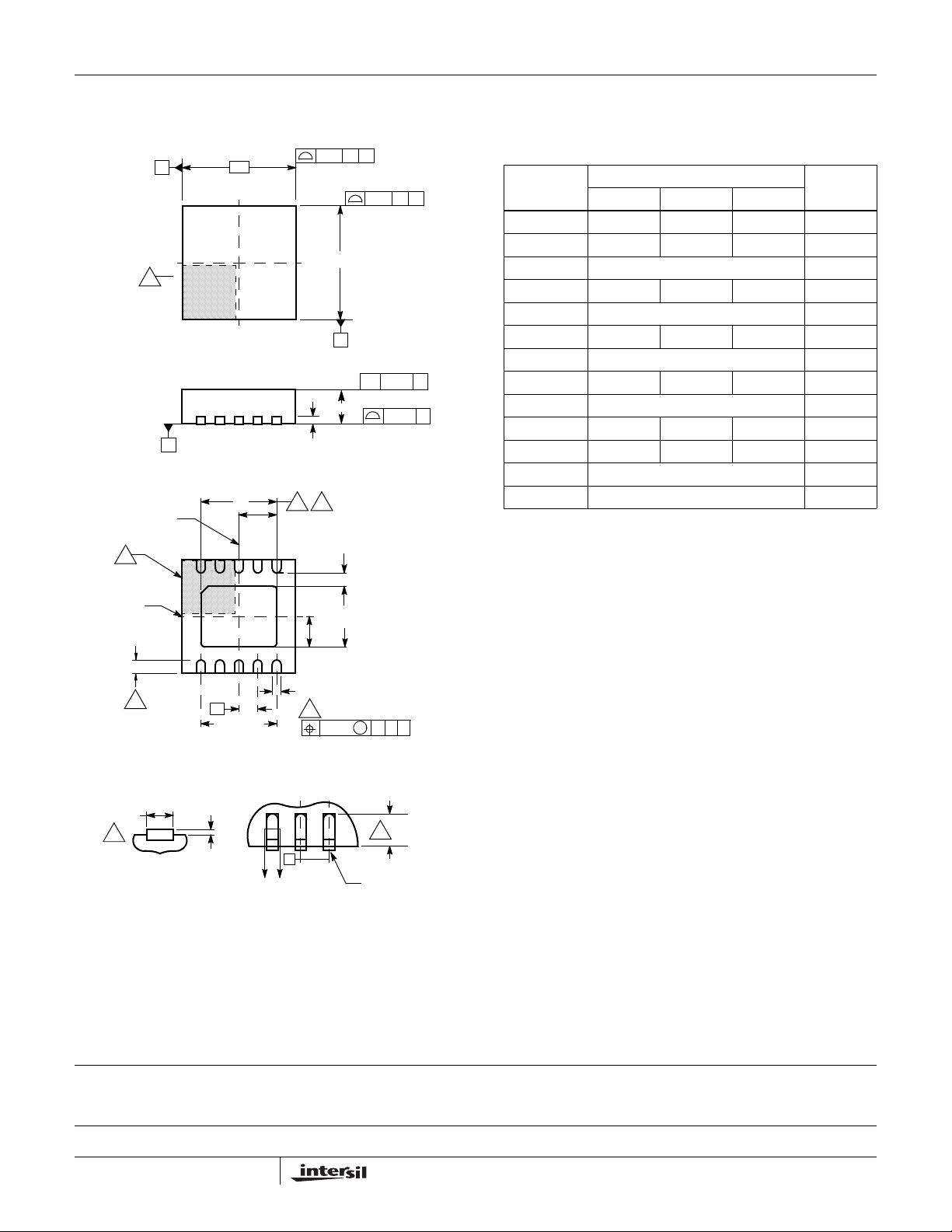
BOOTSTRAP Considerations
Figure 15 shows the upper gate drive (BOOT pin) supplied
by a bootstrap circuit from V
usually shares the V
or VCC supply; it can be any voltage
IN
in the 5V to 12V range. The boot capacitor, C
develops a floating supply voltage referenced to the PHASE
pin. The supply is refreshed to a voltage of V
boot diode drop (V
) each time the lower MOSFET, Q2,
D
turns on. Check that the voltage rating of the capacitor is
above the maximum V
CC
should be sufficient for a 12V system. A value of 0.1µF is
typical for many systems driving single MOSFETs.
If V
is 12V, but VIN is lower (such as 5V), then another
CC
option is to connect the BOOT pin to 12V, and remove the
BOOT cap (although, you may want to add a local capacitor
from BOOT to GND). This will make the UGATE V
equal to (12V - 5V = 7V). That should be high enough to
drive most MOSFETs, and low enough to improve the
efficiency slightly . This also saves a boot diode and
capacitor.
+V
CC
VCC
ISL6341x
-
+
VCC
GND
BOOT
UGATE
PHASE
LGATE/OCSET
. For convenience, VGD
GD
,
BOOT
less the
GD
voltage in the system; a 16V rating
voltage
GS
+V
+V
GD
C
+
D
- V
BOOT
IN
Q1
Q2
V
≈ V
≈ V
GD
CC
- V
D
G-S
V
G-S
When operating with a 12V power supply for V
(or down
CC
to a minimum supply voltage of 4.5V), a wide variety of
N-MOSFETs can be used. Check the absolute maximum
V
rating for both MOSFETs; it needs to be above the
GS
highest V
means a 20V V
30V V
voltage allowed in the system; that usually
CC
maximum rating). Low threshold transistors
DS
rating (which typically correlates with a
GS
(around 1V or below) are not recommended, as explained in
the following.
16
FIGURE 15. UPPER GATE DRIVE BOOTSTRAP
December 2, 2008
FN6538.2
Page 17
ISL6341, ISL6341A, ISL6341B, ISL6341C
Thin Dual Flat No-Lead Plastic Package (TDFN)
(DATUM B)
6
INDEX
AREA
(DATUM A)
NX (b)
5
SECTION "C-C"
6
INDEX
AREA
SEATING
PLANE
NX L
8
A
C
D
TOP VIEW
SIDE VIEW
D2
D2/2
12
N
N-1
e
(Nd-1)Xe
REF.
BOTTOM VIEW
(A1)
2X
A3
E2/2
NX b
5
C
L
e
CC
FOR ODD TERMINAL/SIDE
87
0.10
ABC0.15
2X
0.15
E
//
A
NX k
E2
M
9
TERMINAL TIP
0.10
0.08
L
CB
BAC
L10.3x3B
10 LEAD THIN DUAL FLAT NO-LEAD PLASTIC PACKAGE
MILLIMETERS
SYMBOL
A
A1
A3
b
D
D2
E
C
C
E2
e
k
L
0.70 0.75 0.80
- - 0.05
0.20 REF
0.18 0.25 0.30
3.00 BSC
2.23 2.38 2.48
3.00 BSC
1.49 1.64 1.74
0.50 BSC
0.20 - -
0.30 0.40 0.50
N102
Nd 5 3
NOTES:
1. Dimensioning and tolerancing conform to ASME Y14.5-1994.
2. N is the number of terminals.
3. Nd refers to the number of terminals on D.
4. All dimensions are in millimeters. Angles are in degrees.
5. Dimension b applies to the metallized terminal and is measured
between 0.15mm and 0.30mm from the terminal tip.
6. The configuration of the pin #1 identifier is optional, but must be
located within the zone indicated. The pin #1 identi fier may be
either a mold or mark feature.
7. Dimensions D2 and E2 are for the exposed pads which provide
improved electrical and thermal performance.
8. Nominal dimensions are provided to assist with PCB Land
Pattern Design efforts, see Intersil Technical Brief TB389.
9. COMPLIANT TO JEDEC MO-229-WEED-3 except for
dimensions E2 & D2.
NOTESMIN NOMINAL MAX
-
-
-
5, 8
-
7, 8
-
7, 8
-
-
8
Rev. 0 2/06
All Intersil U.S. products are manufactured, assembled and tested utilizing ISO9000 quality systems.
Intersil Corporation’s quality certifications can be viewed at www.intersil.com/design/quality
Intersil products are sold by description only. Intersil Corporation reserves the right to make changes in circuit design, software and/or specifications at any time without
notice. Accordingly, the reader is cautioned to verify that data sheets are current before placing orders. Information furnished by Intersil is believed to be accurate and
reliable. However, no responsibility is assumed by Intersil or its subsidiaries for its use; nor for any infringements of patents or other rights of third parties which may result
from its use. No license is granted by implicat ion or oth erwise u nde r any p a tent or p at ent r ights of Intersil or its subsidiaries.
For information regarding Intersil Corporation and its products, see www.intersil.com
17
FN6538.2
December 2, 2008
 Loading...