

Page 1
®
ISL6326B
Data Sheet April 21, 2006
4-Phase PWM Controller with 8-Bit DAC
Code Capable of Precision DCR
Differential Current Sensing
The ISL6326B controls microprocessor core voltage
regulation by driving up to 4 synchronous-rectified buck
channels in parallel. Multiphase buck converter architecture
uses interleaved timing to multiply channel ripple frequency
and reduce input and output ripple currents. Lower ripple
results in fewer components, lower component cost, reduced
power dissipation, and smaller implementation area.
Microprocessor loads can generate load transients with
extremely fast edge rates. The ISL6326B utilizes Intersil’s
proprietary Active Pulse Positioning (APP) and Adaptive
Phase Alignment (APA) modulation scheme to achieve the
extremely fast transient response with fewer output
capacitors.
Today’s microprocessors require a tightly regulated output
voltage position versus load current (droop). The ISL6326B
senses the output current continuously by utilizing patented
techniques to measure the voltage across the dedicated
current sense resistor or the DCR of the output inductor. The
sensed current flows out of FB pin to develop the precision
voltage drop across the feedback resistor for droop control.
Current sensing also provides the needed signals for
channel-current balancing, and overcurrent protection. A
programmable integrated temperature compensation
function is implemented to effectively compensate for the
temperature coefficient of the current sense element. The
current limit function provides the overcurrent protection for
the individual phase.
A unity gain, differential amplifier is provided for remote
voltage sensing. Any potential difference between remote
and local grounds can be completely eliminated using the
remote-sense amplifier. Eliminating ground differences
improves regulation and protection accuracy. The thresholdsensitive enable input is available to accurately coordinate
the start up of the ISL6326B with any other voltage rail.
Dynamic-VID™ technology allows seamless on-the-fly VID
changes. The offset pin allows accurate voltage offset
settings that are independent of VID setting.
FN9286.0
Features
• Proprietary Active Pulse Positioning and Adaptive Phase
Alignment Modulation Scheme
• Precision Multiphase Core Voltage Regulation
- Differential Remote Voltage Sensing
- ±0.5% System Accuracy Over Life, Load, Line and
Temperature
- Adjustable Precision Reference-Voltage Offset
• Precision resistor
or DCR Current Sensing
- Accurate Load-Line Programming
- Accurate Channel-Current Balancing
- Differential Current Sense
• Microprocessor Voltage Identification Input
- Dynamic VID™ T echnology
- 8-Bit VID Input with Selectable VR11 Code and
Extended VR10 Code at 6.25mV Per Bit
• Thermal Monitoring
• Integrated Programmable Temperature Compensation
• Overcurrent Protection and Channel Current Limit
• Load Current Indicator and External Overcurrent
Protection Threshold Setup
• Overvoltage Protection
• 2, 3 or 4 Phase Operation
• Adjustable Switching Frequency up to 1MHz Per Phase
• Package Option
- QFN Compliant to JEDEC PUB95 MO-220 QFN - Quad
Flat No Leads - Product Outline
- QFN Near Chip Scale Package Footprint; Improves
PCB Efficiency, Thinner in Profile
• Pb-Free Plus Anneal Available (RoHS Compliant)
Ordering Information
PART
NUMBER
(Note)
ISL6326BCRZ ISL6326BCRZ 0 to70 40 Ld 6x6 QFN L40.6x6
ISL6326BIRZ ISL6326BIRZ -40 to 85 40 Ld 6x6 QFN L40.6x6
Add “-T” suffix for tape and reel.
NOTE: Intersil Pb-free plus anneal products employ special Pb-free
material sets; molding compounds/die attach materials and 100%
matte tin plate termination finish, which are RoHS compliant and
compatible with both SnPb and Pb-free soldering operations. Intersil
Pb-free products are MSL classified at Pb-free peak reflow
temperatures that meet or exceed the Pb-free requirements of
IPC/JEDEC J STD-020.
PART
MARKING
TEMP.
(°C)
PACKAGE
(Pb-Free)
PKG.
DWG. #
1
CAUTION: These devices are sensitive to electrostatic discharge; follow proper IC Handling Procedures.
1-888-INTERSIL or 1-888-468-3774
| Intersil (and design) is a registered trademark of Intersil Americas Inc.
All other trademarks mentioned are the property of their respective owners.
Copyright Intersil Americas Inc. 2006. All Rights Reserved
Page 2
ISL6326B
Pinout
VID6
VID5
VID4
VID3
VID2
VID1
VID0
VRSEL
OFS
DAC
ISL6326B (40 LD QFN)
TOP VIEW
TM
VID7
40
1
2
3
4
5
6
7
8
9
10
11 12 13 14 15 16 17 18 19 20
REF
VR_HOT
39 38 37 36 35 34 33 32 31
FB
COMP
VR_FAN
IOUT
VR_RDY
GND
VDIFF
RGND SS
FS
VSEN
EN_VTT
TCOMP
EN_PWR
VCC
PWM3
PWM1
ISEN3+
30
ISEN3-
29
ISEN2-
28
ISEN2+
27
PWM2
26
PWM4
25
ISEN4+
24
ISEN4-
23
ISEN1-
22
ISEN1+
21
2
FN9286.0
April 21, 2006
Page 3
ISL6326BCR Block Diagram
ISL6326B
RGND
VSEN
SS
VRSEL
VID7
VID6
VID5
VID4
VID3
VID2
VID1
VID0
-
X1
+
+
OVP
-
+175mV
Dynamic
VID
D/A
VDIFF
VR_RDY
SOFTSTART
AND
FAULT LOGIC
FS
CLOCK AND
RAMP GENERATOR
N
APP and APA
MODULATOR
APP and APA
MODULATOR
APP and APA
MODULATOR
POWER-ON
RESET (POR)
0.875
-
+
0.875
-
+
EN_VTT
EN_PWR
PWM1
PWM2
PWM3
DAC
OFS
REF
FB
COMP
IOU T
VR_HOT
VR_FAN
OFFSET
2.0V
-
OCP
+
THERMAL
MONITOR
TM TCOMP
+
E/A
-
I_TRIP
-
OCP
+
TEMPERATURE
COMPENSATION
GAIN ADJUST
APP and APA
MODULATOR
CHANNEL
CURRENT
BALANCE
AND PEAK
CURRENT LIMIT
CHANNEL
DETECT
N
PWM4
ISE N1+
ISEN1ISE N2+
1
N
Σ
TEMPERATURE
COMPENSATION
CHANNEL
CURRENT
SENSE
ISEN2ISE N3+
ISEN3ISE N4+
ISE N4-
GND
3
FN9286.0
April 21, 2006
Page 4
ISL6326B
Typical Application - 4-Phase Buck Converter with Integrated Thermal Compensation
VTT
VR_RDY
VID7
VID6
VID5
VID4
VID3
VID2
VID1
VID0
VRSEL
VR_FAN
VR_HOT
VIN
+5V
COMP
FB
VDIFF
VSEN
RGND
EN_VTT
ISL6326B
EN_PWR
GND
IOUT
TCOMP
TM
+5V
+5V
DACVCC
REF
PWM1
ISEN1-
ISEN1+
PWM2
ISEN2ISEN2+
PWM3
ISEN3-
ISEN3+
PWM4
ISEN4-
ISEN4+
OFS FS SS
+12V
+12V
+12V
+12V
PVCC
VCC
PWM
PVCC
VCC
PWM
PVCC
VCC
PWM
PVCC
ISL6612
DRIVER
ISL6612
DRIVER
ISL6612
DRIVER
BOOT
UGATE
PHASE
LGATE
GND
BOOT
UGATE
PHASE
LGATE
GND
BOOT
UGATE
PHASE
LGATE
GND
BOOT
VIN
VIN
VIN
uP
LOAD
VIN
NTC
VCC
UGATE
PHASE
ISL6612
DRIVER
PWM
4
LGATE
GND
FN9286.0
April 21, 2006
Page 5
ISL6326B
Typical Application - 4-Phase Buck Converter with External Thermal Compensation
NTC
+12V
PWM1
PWM2
+12V
VCC
GND
VCC
ISL6614
DRIVER
BOOT1
UGATE1
PHASE1
LGATE1
PVCC
BOOT2
UGATE2
PHASE2
LGATE2
PGND
BOOT1
5V
To
12V
VIN
VIN
VIN
VTT
VR_RDY
VID7
VID6
VID5
VID4
VID3
VID2
VID1
VID0
VRSEL
VR_FAN
VR_HOT
VIN
o
C
COMP
FB
VDIFF
VSEN
RGND
EN_VTT
ISL6326B
VCC
+5V
DAC
REF
ISEN1+
ISEN1-
PWM1
PWM3
ISEN3-
ISEN3+
ISEN2+
ISEN2-
PWM2
uP
LOAD
EN_PWR
GND
IOUT
TCOMP
TM
+5V
NTC
PWM4
ISEN4-
ISEN4+
OFS FS SS
5
GND
PWM1
PWM2
ISL6614
DRIVER
UGATE1
PHASE1
LGATE1
PVCC
BOOT2
UGATE2
PHASE2
LGATE2
PGND
5V
To
12V
VIN
FN9286.0
April 21, 2006
Page 6
ISL6326B
Absolute Maximum Ratings
Supply Voltage, VCC. . . . . . . . . . . . . . . . . . . . . . . . . . . . . . . . . .+6V
All Pins. . . . . . . . . . . . . . . . . . . . . . . . . . . GND -0.3V to V
ESD (Human Body Model). . . . . . . . . . . . . . . . . . . . . . . . . . . . .>2kV
ESD (Machine Model) . . . . . . . . . . . . . . . . . . . . . . . . . . . . . . .>200V
ESD (Charged Device Model) . . . . . . . . . . . . . . . . . . . . . . . . >1.5kV
CC
+ 0.3V
Thermal Information
Thermal Resistance (Notes 1, 2) θ
QFN Package. . . . . . . . . . . . . . . . . . . . 32 3.5
Maximum Junction Temperature . . . . . . . . . . . . . . . . . . . . . . . 150°C
Maximum Storage Temperature Range. . . . . . . . . . .-65°C to 150°C
Maximum Lead Temperature (Soldering 10s) . . . . . . . . . . . . . 300°C
(°C/W) θ
JA
JC
(°C/W)
Operating Conditions
Supply Voltage, VCC . . . . . . . . . . . . . . . . . . . . . . . . . . . . +5V ±5%
Ambient Temperature (ISL6326BCRZ) . . . . . . . . . . . . . 0°C to 70°C
Ambient Temperature (ISL6326BIRZ) . . . . . . . . . . . . .-40°C to 85°C
CAUTION: Stress above those listed in “Absolute Maximum Ratings” may cause permanent damage to the device. This is a stress only rating and operation of the
device at these or any other conditions above those indicated in the operational section of this specification is not implied.
NOTES:
is measured in free air with the component mounted on a high effective thermal conductivity test board with “direct attach” features. See
1. θ
JA
Tech Brief TB379
2. For θ
, the “case temp” location is the center of the exposed metal pad on the package underside.
JC
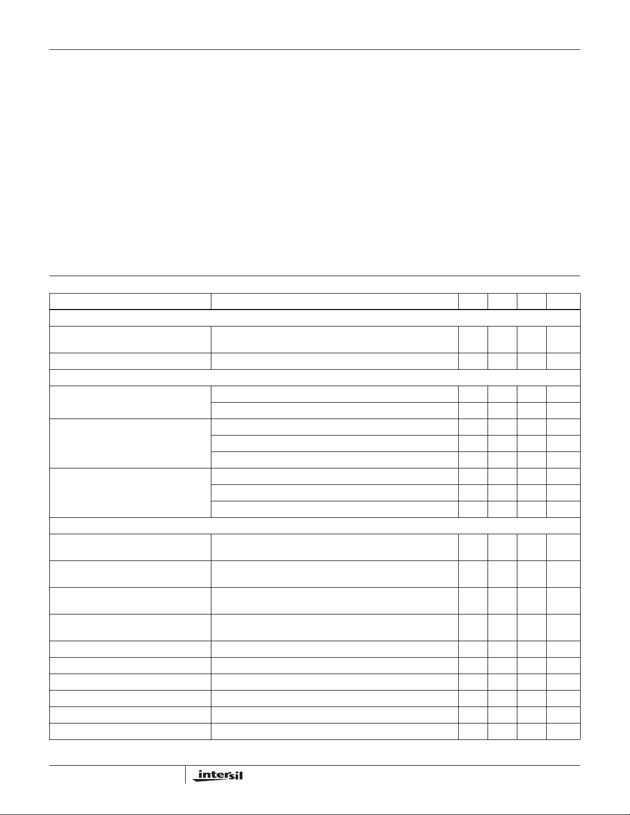
Electrical Specifications Operating Conditions: VCC = 5V, Unless Otherwise Specified
PARAMETER TEST CONDITIONS MIN TYP MAX UNITS
VCC SUPPLY CURRENT
Nominal Supply VCC = 5VDC; EN_PWR = 5VDC; R
ISEN1 = ISEN2 = ISEN3 = ISEN4 = -70μA
Shutdown Supply VCC = 5VDC; EN_PWR = 0VDC; R
POWER-ON RESET AND ENABLE
POR Threshold VCC Rising 4.3 4.5 4.7 V
VCC Falling 3.7 3.9 4.2 V
EN_PWR Threshold Rising 0.850 0.875 0.910 V
Hysteresis - 130 - mV
Falling 0.720 0.745 0.775 V
EN_VTT Threshold Rising 0.850 0.875 0.910 V
Hysteresis - 130 - mV
Falling 0.720 0.745 0.775 V
REFERENCE VOLTAGE AND DAC
System Accuracy of ISL6326BCRZ
(VID = 1V-1.6V, T
= 0°C to 70°C)
J
System Accuracy of ISL6326BCRZ
(VID = 0.5V-1V, T
= 0°C to 70°C)
J
System Accuracy of ISL6326BIRZ
(VID = 1V-1.6V, T
= -40°C to 85°C)
J
System Accuracy of ISL6326BIRZ
(VID = 0.5V-1V, T
= -40°C to 85°C)
J
(Note 3) -0.5 - 0.5 %VID
(Note 3) -0.9 - 0.9 %VID
(Note 3) -0.6 - 0.6 %VID
(Note 3) -1 - 1 %VID
VID Pull Up -60 -40 -20 µA
VID Input Low Level --0.4V
VID Input High Level 0.8 - - V
VRSEL Input Low Level --0.4V
VRSEL Input High Level 0.8 - - V
DAC Source Current -47mA
= 100kΩ,
T
= 100kΩ -1421mA
T
-1826mA
6
FN9286.0
April 21, 2006
Page 7
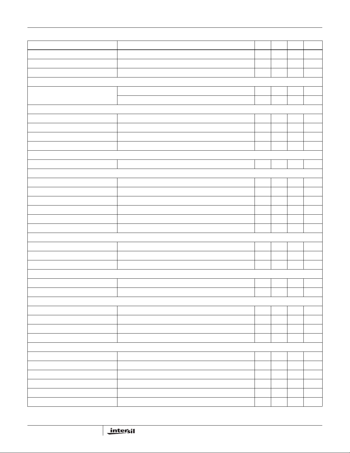
ISL6326B
Electrical Specifications Operating Conditions: VCC = 5V, Unless Otherwise Specified (Conti nued)
PARAMETER TEST CONDITIONS MIN TYP MAX UNITS
DAC Sink Current - - 300 µA
REF Source Current 45 50 55 µA
REF Sink Current 45 50 55 µA
PIN-ADJUSTABLE OFFSET
Voltage at OFS Pin Offset resistor connected to ground 380 400 420 mV
Voltage below VCC, offset resistor connected to VCC 1.55 1.60 1.65 V
OSCILLATORS
Accuracy of Switching Frequency Setting R
Adjustment Range of Switching Frequency (Note 4) 0.08 - 1.0 MHz
Soft-start Ramp Rate R
Adjustment Range of Soft-Start Ramp Rate (Note 4) 0.625 - 6.25 mV/µs
PWM GENERATOR
Sawtooth Amplitude -1.25- V
ERROR AMPLIFIER
Open-Loop Gain R
Open-Loop Bandwidth (Note 4) - 80 - MHz
Slew Rate (Note 4) - 25 - V/µs
Maximum Output Voltage 3.8 4.3 4.9 V
Output High Voltage @ 2mA 3.6 - - V
Output Low Voltage @ 2mA --1.8V
REMOTE-SENSE AMPLIFIER
Bandwidth (Note 4) - 20 - MHz
Output High Current VSEN - RGND = 2.5V -500 - 500 µA
Output High Current VSEN - RGND = 0.6 -500 - 500 µA
PWM OUTPUT
PWM Output Voltage LOW Threshold Iload = ±500μA--0.5V
PWM Output Voltage HIGH Threshold Iload = ±500μA4.3--V
CURRENT SENSE AND OVERCURRENT PROTECTION
Sensed Current Tolerance (IOUT) ISEN1 = ISEN2 = ISEN3 = ISEN4 = 60μA 576063µA
Overcurrent Trip Level for Average Current 72 85 98 µA
Peak Current Limit for Individual Channel 100 120 140 µA
IOUT Trip Level for Overcurrent protection 1.85 2.0 2.15 V
THERMAL MONITORING AND FAN CONTROL
TM Input Voltage for VR_FAN Trip 1.55 1.65 1.75 V
TM Input Voltage for VR_FAN Reset 1.85 1.95 2.05 V
TM Input Voltage for VR_HOT Trip 1.30 1.40 1.50 V
TM Input Voltage for VR_HOT Reset 1.55 1.65 1.75 V
Leakage Current of VR_FAN With externally pull-up resistor connected to VCC - - 30 µA
VR_FAN Low Voltage With 1.25k resistor pull-up to VCC, I
= 100kΩ 225 250 275 kHz
T
= 100kΩ (Notes 5, 6) - 1.563 - mV/µs
S
= 10kΩ to ground (Note 4) - 96 - dB
L
= 4mA - - 0.4 V
VR_FAN
7
FN9286.0
April 21, 2006
Page 8
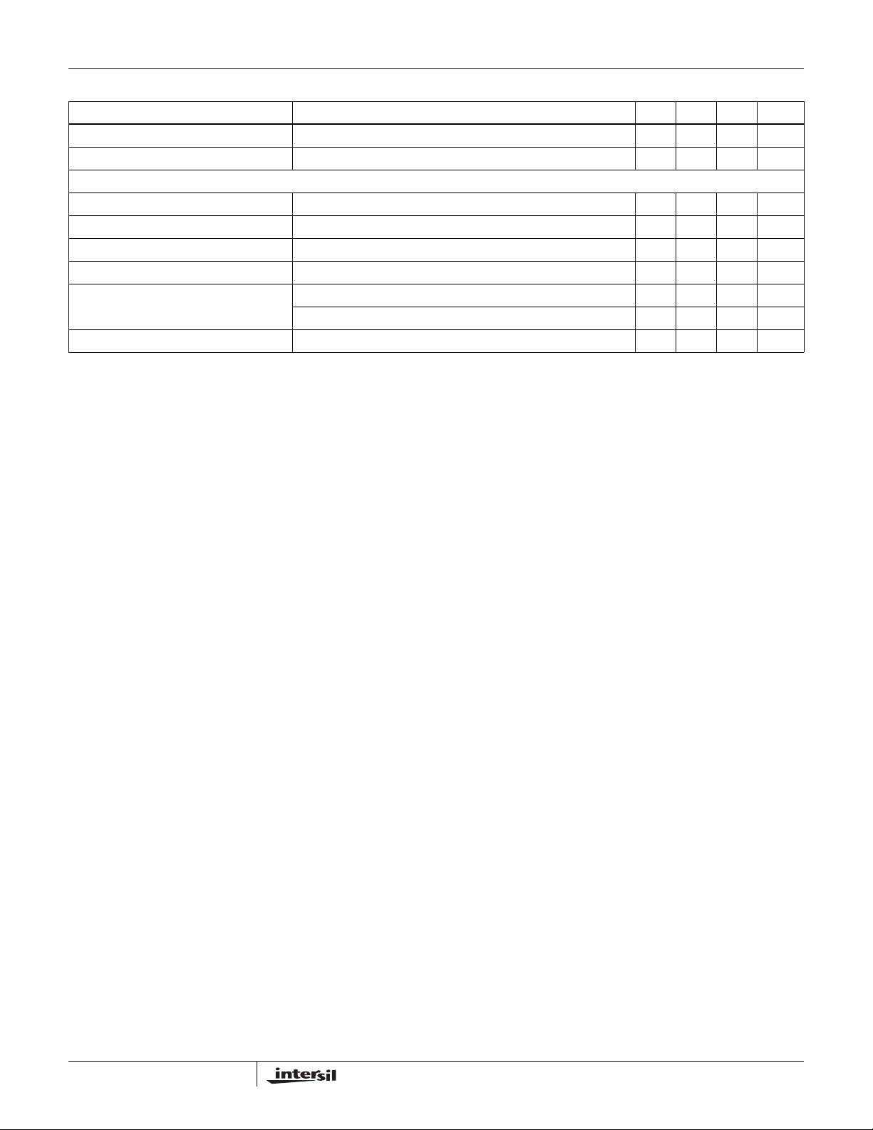
ISL6326B
Electrical Specifications Operating Conditions: VCC = 5V, Unless Otherwise Specified (Conti nued)
PARAMETER TEST CONDITIONS MIN TYP MAX UNITS
Leakage Current of VR_HOT With externally pull-up resistor connected to VCC - - 30 µA
VR_HOT Low Voltage With 1.25k resistor pull-up to VCC, I
VR READY AND PROTECTION MONITORS
Leakage Current of VR_RDY With externally pull-up resistor connected to VCC - - 30 μA
VR_RDY Low Voltage I
Undervoltage Threshold VDIFF Falling 48 50 52 %VID
VR_RDY Reset Voltage VDIFF Rising 58 60 62 %VID
Overvoltage Protection Threshold Before valid VID 1.250 1.275 1.300 V
After valid VID, the voltage above VID 150 175 200 mV
Overvoltage Protection Reset Hysteresis - 100 - mV
NOTES:
3. These parts are designed and adjusted for accuracy with all errors in the voltage loop included.
4. Spec guaranteed by design.
5. During soft-start, VDAC rises from 0 to 1.1V first and then ramp to VID voltage after receiving valid VID.
6. Soft-start ramp rate is determined by the adjustable soft-start oscillator frequency at the speed of 6.25mV per cycle.
= 4mA - - 0.4 V
VR_RDY
= 4mA - - 0.4 V
VR_HOT
8
FN9286.0
April 21, 2006
Page 9

ISL6326B
Functional Pin Description
VCC - Supplies the power necessary to operate the chip.
The controller starts to operate when the voltage on this pin
exceeds the rising POR threshold and shuts down when the
voltage on this pin drops below the falling POR threshold.
Connect this pin directly to a +5V supply.
GND - Bias and reference ground for the IC. The bottom
metal base of ISL6326B is the GND.
EN_PWR - This pin is a threshold-sensitive enable input for
the controller. Connecting the 12V supply to EN_PWR
through an appropriate resistor divider provides a means to
synchronize power-up of the controller and the MOSFET
driver ICs. When EN_PWR is driven above 0.875V, the
ISL6326B is active depending on status of EN_VTT, the
internal POR, and pending fault states. Driving EN_PWR
below 0.745V will clear all fault states and prime the
ISL6326B to soft-start when re-enabled.
EN_VTT - This pin is another threshold-sensitive enable
input for the controller. It’s typically connected to VTT output
of VTT voltage regulator in the computer mother board.
When EN_VTT is driven above 0.875V, the ISL6326B is
active depending on status of EN_PWR, the internal POR,
and pending fault states. Driving EN_VTT below 0.745V will
clear all fault states and prime the ISL6326B to soft-start
when re-enabled.
FS - Use this pin to set up the desired switching frequency. A
resistor, placed from FS to ground will set the switching
frequency. The relationship between the value of the resistor
and the switching frequency will be described by an
approximate equation.
SS - Use this pin to set up the desired start-up oscillator
frequency. A resistor, placed from SS to ground will set up
the soft-start ramp rate. The relationship between the value
of the resistor and the soft-start ramp up time will be
described by an approximate equation.
VID7, VID6, VID5, VID4, VID3, VID2, VID1 and VID0 -
These are the inputs to the internal DAC that generates the
reference voltage for output regulation. Connect these pins
either to open-drain outputs with or without external pull-up
resistors or to active-pull-up outputs. All VID pins have 40µA
internal pull-up current sources that diminish to zero as the
voltage rises above the logic-high level. These inputs can be
pulled up externally as high as VCC plus 0.3V.
VRSEL - use this pin to select internal VID code. When it is
connected to GND, the extended VR10 code is selected.
When it’s floated or pulled to high, VR11 code is selected.
This input can be pulled up as high as VCC plus 0.3V.
VDIFF, VSEN, and RGND - VSEN and RGND form the
precision differential remote-sense amplifier. This amplifier
converts the differential voltage of the remote output to a
single-ended voltage referenced to local ground. VDIFF is
the amplifier’s output and the input to the regulation and
protection circuitry. Connect VSEN and RGND to the sense
pins of the remote load.
FB and COMP - Inverting input and output of the error
amplifier respectively. FB can be connected to VDIFF
through a resistor. A properly chosen resistor between
VDIFF and FB can set the load line (droop), because the
sensed current will flow out of FB pin. The droop scale factor
is set by the ratio of the ISEN resistors and the inductor DCR
or the dedicated current sense resistor. COMP is tied back to
FB through an external R-C network to compensate the
regulator.
DAC and REF - The DAC pin is the output of the precision
internal DAC reference. The REF pin is the positive input of
the Error Amp. In typical applications, a 1kΩ, 1% resistor is
used between DAC and REF to generate a precision offset
voltage. This voltage is proportional to the offset current
determined by the offset resistor from OFS to ground or
VCC. A capacitor is used between REF and ground to
smooth the voltage transition during Dynamic VID™
operations.
PWM1, PWM2, PWM3, PWM4 - Pulse width modulation
outputs. Connect these pins to the PWM input pins of the
Intersil driver IC. The number of active channels is
determined by the state of PWM3 and PWM4. Tie PWM3 to
VCC to configure for 2-phase operation. Tie PWM4 to VCC
to configure for 3-phase operation.
ISEN1+, ISEN1-; ISEN2+, ISEN2-; ISEN3+, ISEN3-;
ISEN4+, ISEN4- - The ISEN+ and ISEN- pins are current
sense inputs to individual differential amplifiers. The sensed
current is used for channel current balancing, overcurrent
protection, and droop regulation. Inactive channels should
have their respective current sense inputs left open (for
example, open ISEN4+ and ISEN4- for 3-phase operation).
For DCR sensing, connect each ISEN- pin to the node
between the RC sense elements. Tie the ISEN+ pin to the
other end of the sense capacitor through a resistor, R
ISEN
.
The voltage across the sense capacitor is proportional to the
inductor current. Therefore, the sense current is proportional
to the inductor current, and scaled by the DCR of the
inductor and R
ISEN
.
To match the time delay of the internal circuit, a capacitor is
needed between each ISEN+ pin and GND, as described in
the Current Sensing section.
VR_RDY - VR_RDY indicates that soft-start has completed
and the output voltage is within the regulated range around
VID setting. It is an open-drain logic output. When OCP or
OVP occurs, VR_RDY will be pulled to low. It will also be
pulled low if the output voltage is below the under-voltage
threshold.
9
FN9286.0
April 21, 2006
Page 10
ISL6326B
OFS - The OFS pin can be used to program a DC offset
current which will generate a DC offset voltage between the
REF and DAC pins. The offset current is generated via an
external resistor and precision internal voltage references.
The polarity of the offset is selected by connecting the
resistor to GND or VCC. For no offset, the OFS pin should
be left unterminated.
TCOMP - Temperature compensation scaling input. The
voltage sensed on the TM pin is utilized as the temperature
input to adjust ldroop and the overcurrent protection limit to
effectively compensate for the temperature coefficient of the
current sense element. To implement the integrated
temperature compensation, a resistor divider circuit is
needed with one resistor being connected from TCOMP to
VCC of the controller and another resistor being connected
from TCOMP to GND. Changing the ratio of the resistor
values will set the gain of the integrated thermal
compensation. When integrated temperature compensation
function is not used, connect TCOMP to GND.
IOUT - IOUT is the output pin of sensed average channel
current. In actual application, a resistor needs to be placed
between IOUT and GND to ensure the proper operation. The
voltage at IOUT pin will be proportional to the load current
and the resistor value. ISL6326B monitors the voltage at
IOUT for overcurrent protection. If the voltage at IOUT pin is
higher than 2V, it will trigger the overcurrent shutdown. By
choosing the proper value for the resistor at IOUT pin, the
overcurrent trip level can be set to be lower than the fixed
internal overcurrent threshold. Tie it to GND if not used.
TM - TM is an input pin for the VR temperature
measurement. Connect this pin through an NTC thermistor
to GND and a resistor to VCC of the controller. The voltage
at this pin is reverse proportional to the VR temperature.
ISL6326B monitors the VR temperature based on the
voltage at the TM pin and outputs VR_HOT and VR_FAN
signals.
Operation
Multiphase Power Conversion
Microprocessor load current profiles have changed to the
point that the advantages of multiphase power conversion
are impossible to ignore. The technical challenges
associated with producing a single-phase converter which is
both cost-effective and thermally viable have forced a
change to the cost-saving approach of multiphase. The
ISL6326B controller helps reduce the complexity of
implementation by integrating vital functions and requiring
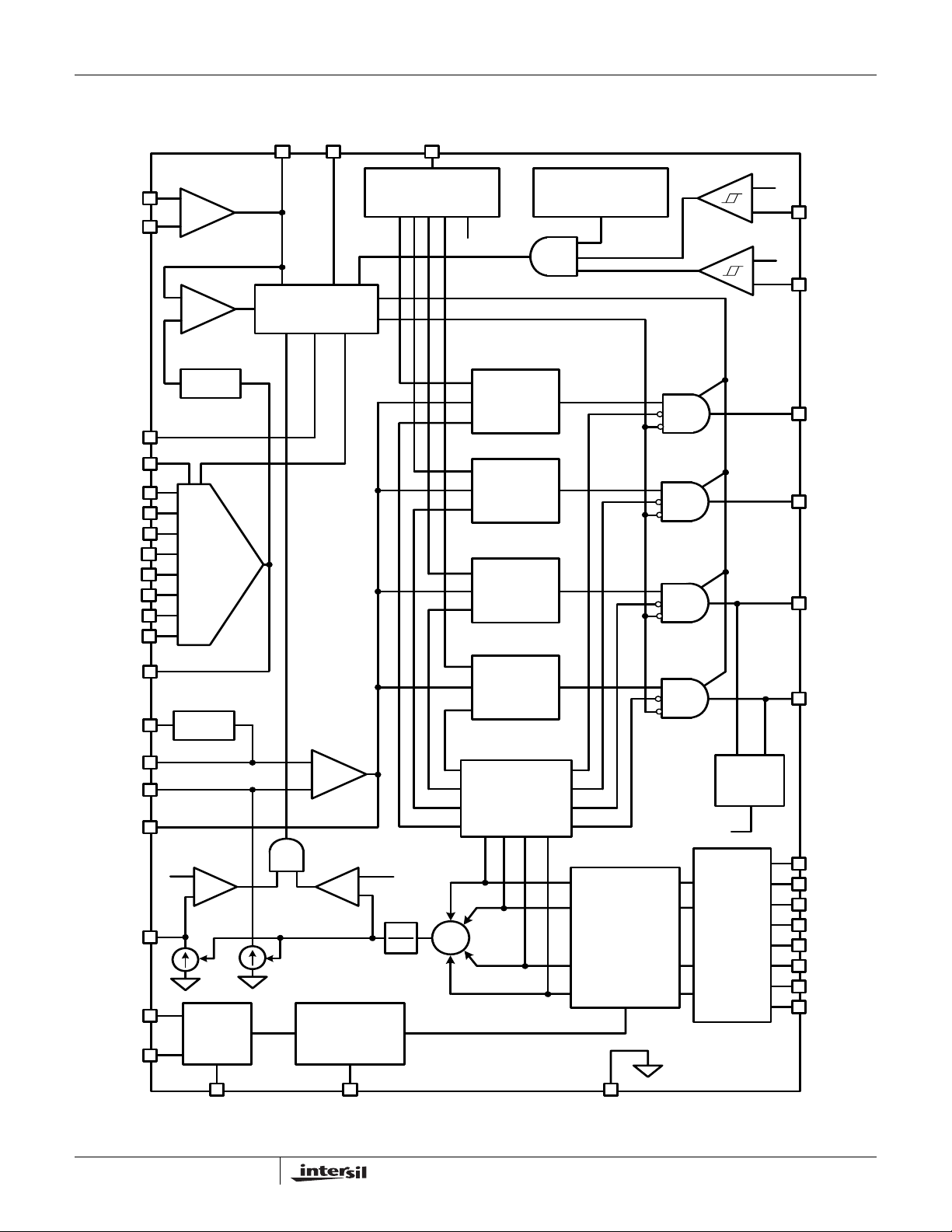
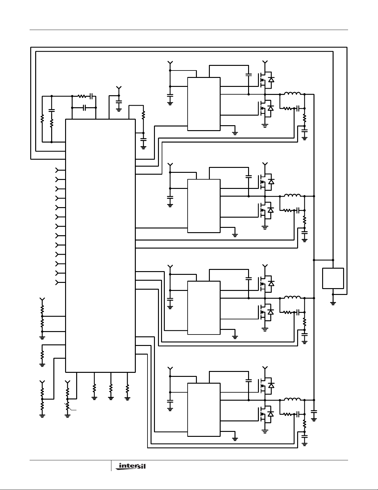
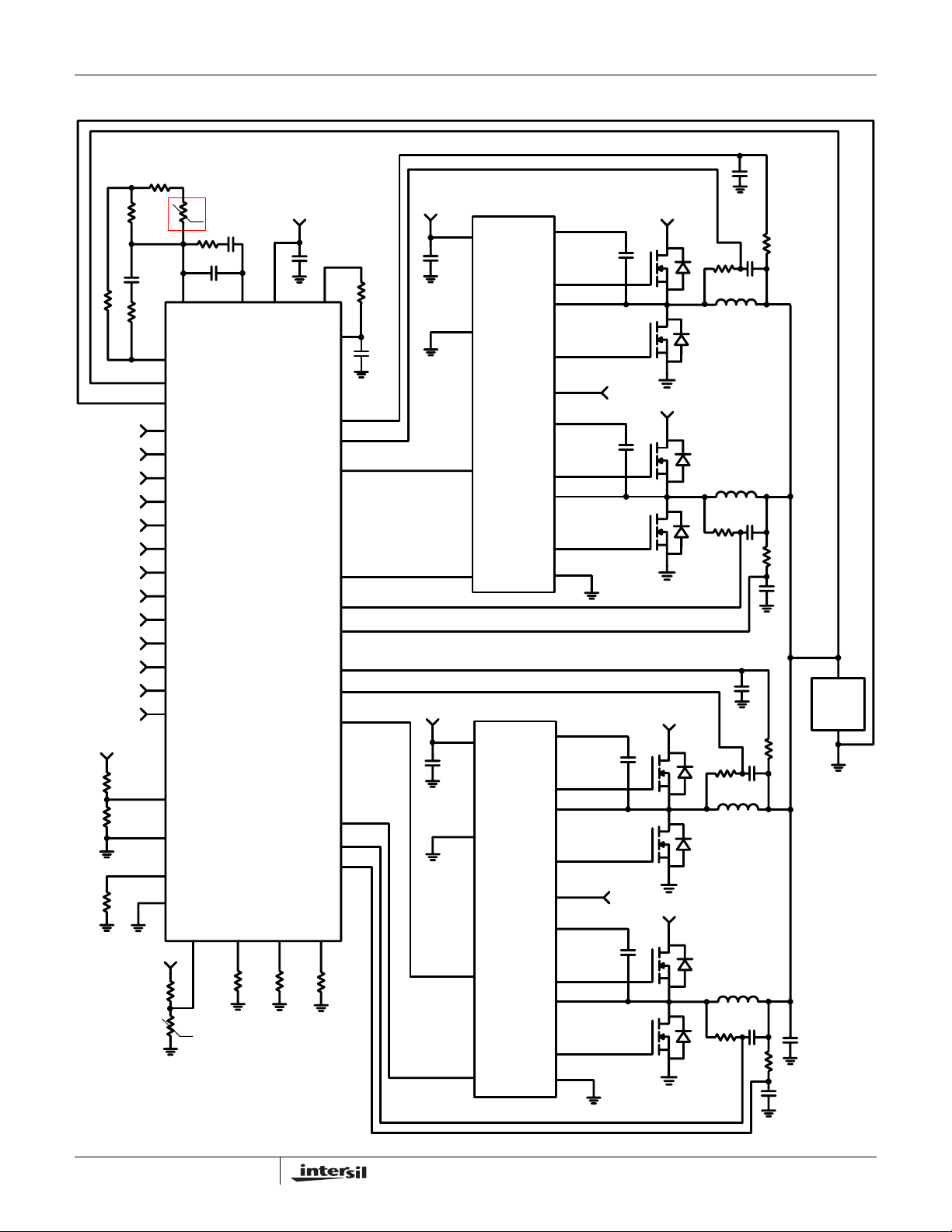
minimal output components. The block diagrams on pages
3, 4, and 5 provide top level views of multiphase power
conversion using the ISL6326B controller.
Interleaving
The switching of each channel in a multiphase converter is
timed to be symmetrically out of phase with each of the other
channels. In a 3-phase converter, each channel switches 1/3
cycle after the previous channel and 1/3 cycle before the
following channel. As a result, the three-phase converter has
a combined ripple frequency three times greater than the
ripple frequency of any one phase. In addition, the peak-topeak amplitude of the combined inductor currents is reduced
in proportion to the number of phases (Equations 1 and 2).
Increased ripple frequency and lower ripple amplitude mean
that the designer can use less per-channel inductance and
lower total output capacitance for any performance
specification.
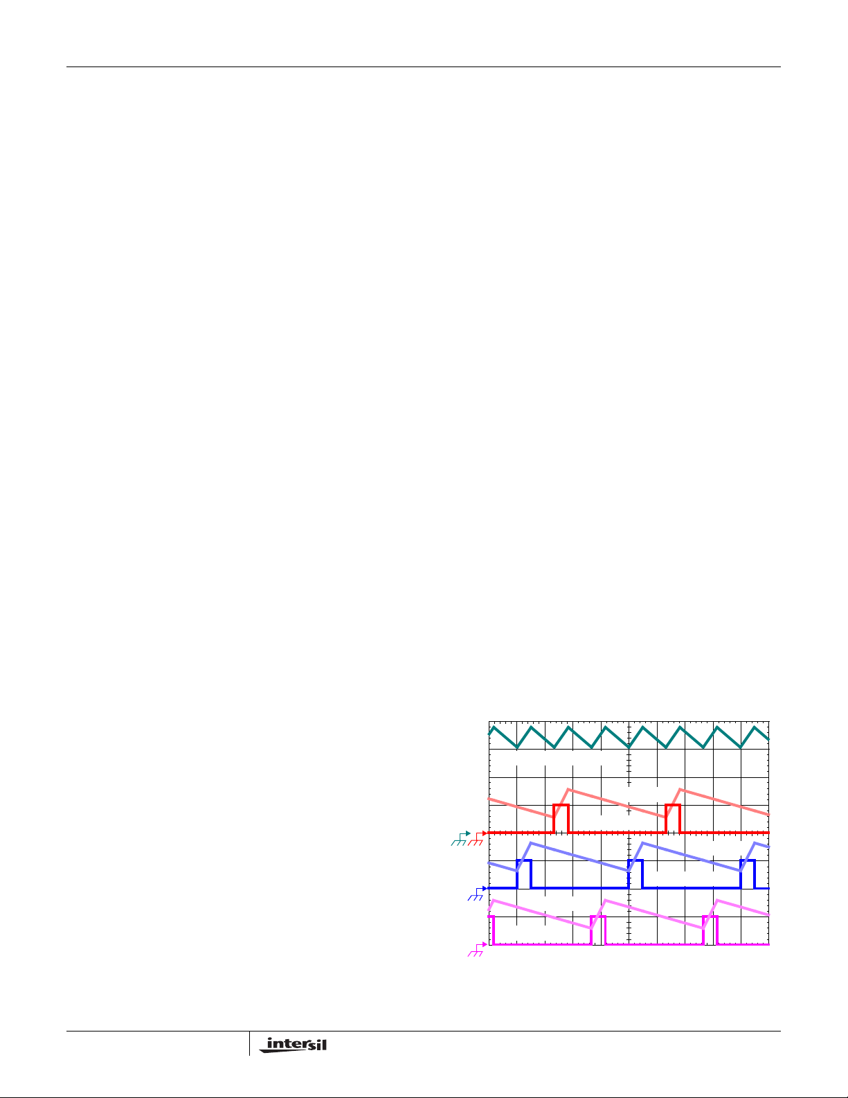
Figure 1 illustrates the multiplicative effect on output ripple
frequency. The three channel currents (IL1, IL2, and IL3)
combine to form the AC ripple current and the DC load
current. The ripple component has three times the ripple
frequency of each individual channel current. Each PWM
pulse is terminated 1/3 of a cycle after the PWM pulse of the
previous phase. The DC components of the inductor currents
combine to feed the load.
VR_HOT - VR_HOT is used as an indication of high VR
temperature. It is an open-drain logic output. It will be pulled
low if the measured VR temperature is less than a certain
level, and open when the measured VR temperature
reaches a certain level. A external pull-up resistor is needed.
VR_FAN - VR_FAN is an output pin with open-drain logic
output. It will be pulled low if the measured VR temperature
is less than a certain level, and open when the measured VR
temperature reaches a certain level. A external pull-up
resistor is needed.
10
IL1 + IL2 + IL3, 7A/DIV
IL1, 7A/DIV
PWM1, 5V/DIV
IL2, 7A/DIV
PWM2, 5V/DIV
IL3, 7A/DIV
PWM3, 5V/DIV
1µs/DIV
FIGURE 1. PWM AND INDUCTOR-CURRENT WAVEFORMS
FOR 3-PHASE CONVERTER
FN9286.0
April 21, 2006
Page 11
ISL6326B
T o understand the reduction of ripple current amplitude in the
multiphase circuit, examine the equation representing an
individual channel’s peak-to-peak inductor current.
VINV
–()V
OUT
I
------------------------------------------------------=
PP
LfSV
In Equation 1, V
IN
and V
IN
OUT
are the input and output
OUT
(EQ. 1)
voltages respectively, L is the single-channel inductor value,
and f
is the switching frequency.
S
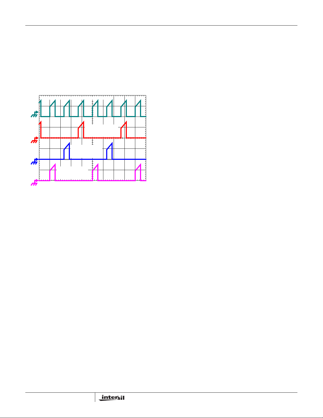
INPUT-CAPACITOR CURRENT, 10A/DIV
CHANNEL 1
INPUT CURRENT
10A/DIV
CHANNEL 2
INPUT CURRENT
10A/DIV
CHANNEL 3
INPUT CURRENT
10A/DIV
1µs/DIV
FIGURE 2. CHANNEL INPUT CURRENTS AND INPUT-
CAPACITOR RMS CURRENT FOR 3-PHASE
CONVERTER
The output capacitors conduct the ripple component of the
inductor current. In the case of multiphase converters, the
capacitor current is the sum of the ripple currents from each
of the individual channels. Compare Equation 1 to the
expression for the peak-to-peak current after the summation
of N symmetrically phase-shifted inductor currents in
Equation 2. Peak-to-peak ripple current decreases by an
amount proportional to the number of channels. Outputvoltage ripple is a function of capacitance, capacitor
equivalent series resistance (ESR), and inductor ripple
current. Reducing the inductor ripple current allows the
designer to use fewer or less costly output capacitors.
VINNV
–()V
OUT
IN
OUT
(EQ. 2)
I
------------------------------------------------------------=
CPP,
LfSV
Another benefit of interleaving is to reduce input ripple
current. Input capacitance is determined in part by the
maximum input ripple current. Multiphase topologies can
improve overall system cost and size by lowering input ripple
current and allowing the designer to reduce the cost of input
capacitance. The example in Figure 2 illustrates input
currents from a three-phase converter combining to reduce
the total input ripple current.
The converter depicted in Figure 2 delivers 36A to a 1.5V load
from a 12V input. The RMS input capacitor current is 5.9A.
Compare this to a single-phase converter also stepping down
12V to 1.5V at 36A. The single-phase converter has 11.9A
RMS input capacitor current. The single-phase converter
must use an input capacitor bank with twice the RMS current
capacity as the equivalent three-phase converter .
Figures 17, 18 and 19 in the section entitled Input Capacitor
Selection can be used to determine the input-capacitor RMS
current based on load current, duty cycle, and the number of
channels. They are provided as aids in determining the
optimal input capacitor solution. Figure 20 shows the single
phase input-capacitor RMS current for comparison.
PWM Modulation Scheme
The ISL6326B adopts Intersil's proprietary Active Pulse
Positioning (APP) modulation scheme to improve transient
performance. APP control is a unique dual-edge PWM
modulation scheme with both PWM leading and trailing
edges being independently moved to give the best response
to transient loads. The PWM frequency, however , is constant
and set by the external resistor between the FS pin and
GND. To further improve the transient response, the
ISL6326B also implements Intersil's proprietary Adaptive
Phase Alignment (APA) technique. APA, with sufficiently
large load step currents, can turn on all phases together.
With both APP and APA control, ISL6326B can achieve
excellent transient performance and reduce the demand on
the output capacitors.
Under steady state conditions the operation of the ISL6326B
PWM modulator appears to be that of a conventional trailing
edge modulator. Conventional analysis and design methods
can therefore be used for steady state and small signal
operation.
PWM Operation
The timing of each channel is set by the number of active
channels. The default channel setting for the ISL6326B is
four. The switching cycle is defined as the time between
PWM pulse termination signals of each channel. The cycle
time of the pulse signal is the inverse of the switching
frequency set by the resistor between the FS pin and
ground. The PWM signals command the MOSFET driver to
turn on/off the channel MOSFETs.
For 4-channel operation, the channel firing order is 4-3-2-1:
PWM3 pulse happens 1/4 of a cycle after PWM4, PWM2
output follows another 1/4 of a cycle after PWM3, and
PWM1 delays another 1/4 of a cycle after PWM2. For
3-channel operation, the channel firing order is 3-2-1.
Connecting PWM4 to VCC selects three channel operation
and the pulse times are spaced in 1/3 cycle increments. If
PWM3 is connected to VCC, two channel operation is
selected and the PWM2 pulse happens 1/2 of a cycle after
PWM pulse.
Switching Frequency
Switching frequency is determined by the selection of the
frequency-setting resistor, R
pin to GND (see the figures labelled Typical Applications on
, which is connected from FS
T
11
FN9286.0
April 21, 2006
Page 12
ISL6326B
pages 4 and 5). Equation 3 is provided to assist in selecting
the correct resistor value.
10
2.5X10
R
------------------------- -=
T
where F
F
SW
is the switching frequency of each phase.
SW
(EQ. 3)
Current Sensing
ISL6326B senses the current continuously for fast response.
ISL6326B supports inductor DCR sensing, or resistive
sensing techniques. The associated channel current sense
amplifier uses the ISEN inputs to reproduce a signal
proportional to the inductor current, I
I
, is proportional to the inductor current. The sensed
SEN
current is used for current balance, load-line regulation, and
overcurrent protection.
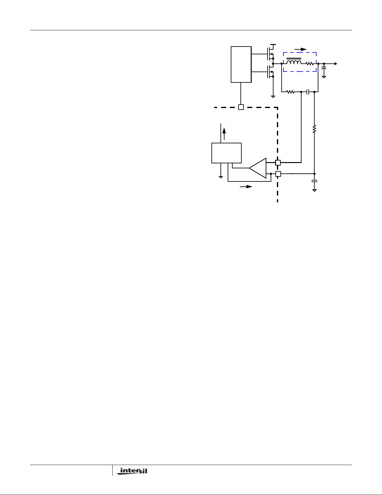
The internal circuitry, shown in Figures 3, and 4, represents
one channel of an N-channel converter. This circuitry is
repeated for each channel in the converter, but may not be
active depending on the status of the PWM3 and PWM4
pins, as described in the PWM Operation section.
INDUCTOR DCR SENSING
An inductor’s winding is characteristic of a distributed
resistance as measured by the DCR (Direct Current
Resistance) parameter. Consider the inductor DCR as a
separate lumped quantity, as shown in Figure 3. The
channel current I
, flowing through the inductor, will also
L
pass through the DCR. Equation 4 shows the s-domain
equivalent voltage across the inductor V
V
LIL
sL DCR+⋅()⋅=
A simple R-C network across the inductor extracts the DCR
voltage, as shown in Figure 3.
The voltage on the capacitor V
proportional to the channel current I
L
⎛⎞
-------------
s
⋅ 1+
⎝⎠
DCR
---------------------------------------------------------------------
V
=
C
sRC 1+⋅()
DCR I
⋅()⋅
L
If the R-C network components are selected such that the
RC time constant (= R*C) matches the inductor time
constant (= L/DCR), the voltage across the capacitor V
equal to the voltage drop across the DCR, i.e., proportional
to the channel current.
. The sense current,
L
.
L
, can be shown to be
C
, see Equation 5.
L
(EQ. 4)
(EQ. 5)
is
C
V
IN
ISL6605
PWM(n)
ISL6326B INTERNAL CIRCUIT
In
CURRENT
SENSE
I
=
SEN
FIGURE 3. DCR SENSING CONFIGURATION
I
L
DCR
----------------- -
R
ISEN
+
-
L
INDUCTOR
R
ISEN-(n)
ISEN+(n)
ILs()
V
+
L
+
DCR
VC(s)
C
V
OUT
C
-
R
ISEN(n)
(PTC)
C
T
OUT
-
With the internal low-offset current amplifier, the capacitor
voltage V
Therefore, the current out of ISEN+ pin, I
is replicated across the sense resistor R
C
, is proportional
SEN
ISEN
.
to the inductor current.
Because of the internal filter at ISEN- pin, one capacitor, C
T
is needed to match the time delay between the ISEN- and
ISEN+ signals. Select the proper C
constant of R
ISEN
and CT (R
to keep the time
T
x CT ) close to 27ns.
ISEN
Equation 6 shows that the ratio of the channel current to the
sensed current, I
, is driven by the value of the sense
SEN
resistor and the DCR of the inductor.
DCR
I
SENIL
----------------- -
⋅=
R
ISEN
(EQ. 6)
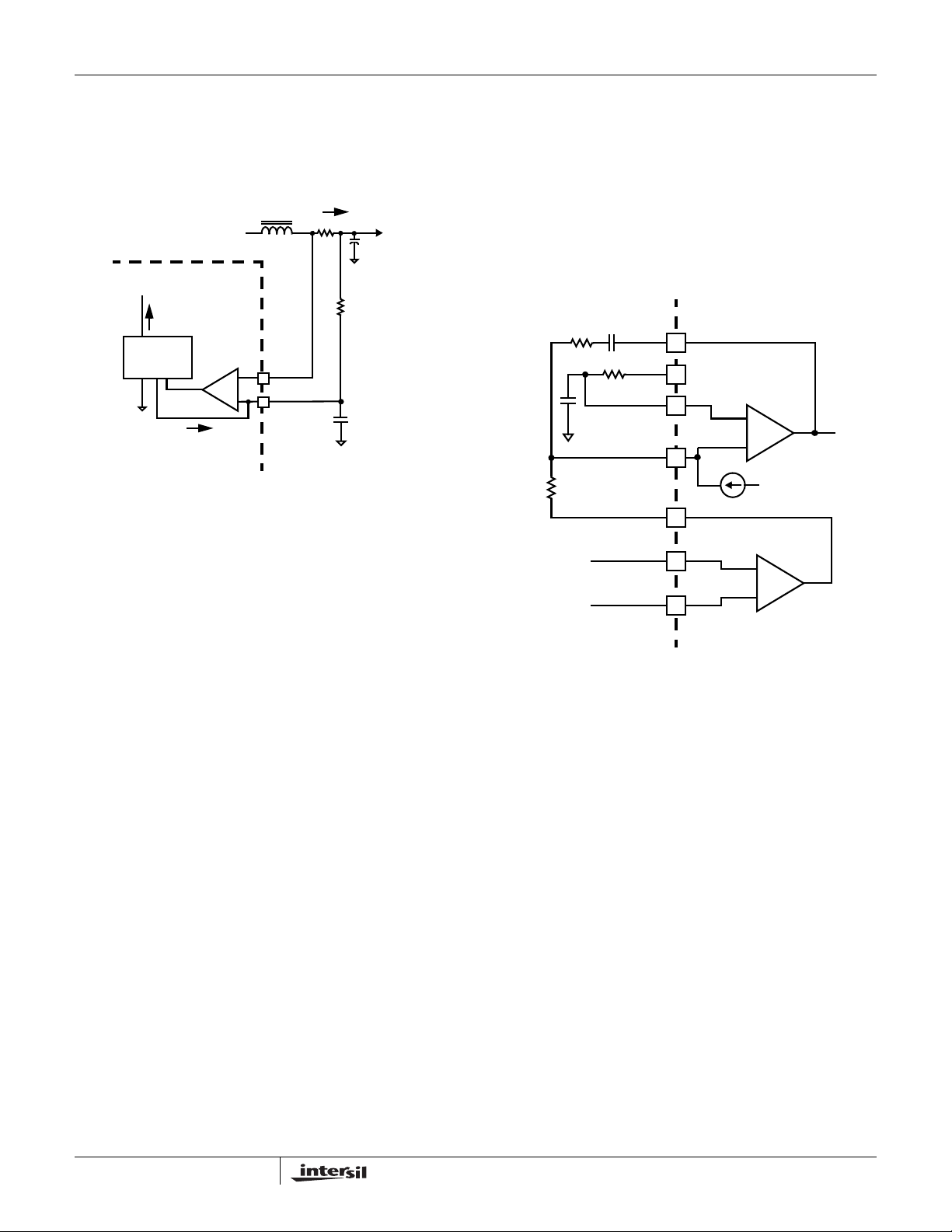
RESISTIVE SENSING
For accurate current sense, a dedicated current-sense
resistor R
in series with each output inductor can
SENSE
serve as the current sense element (see Figure 4). This
technique is more accurate, but reduces overall converter
efficiency due to the additional power loss on the current
sense element R
SENSE
.
The same capacitor CT is needed to match the time delay
between ISEN- and ISEN+ signals. Select the proper C
keep the time constant of R
ISEN
and CT (R
x CT ) close
ISEN
T
to
to 27ns.
,
12
FN9286.0
April 21, 2006
Page 13
ISL6326B
Equation 7 shows the ratio of the channel current to the
sensed current I
R
SENSE
I
SENIL
FIGURE 4. SENSE RESISTOR IN SERIES WITH INDUCTORS
-----------------------
⋅=
R
ISL6326B INTERNAL CIRCUIT
In
CURRENT
SENSE
I
SEN
SEN
ISEN
I
L
.
R
SENSE
--------------------------=
R
ISEN
(EQ. 7)
I
L
ISEN-(n)
+
-
ISEN+(n)
L
R
SENSE
C
R
ISEN(n)
C
T
V
OUT
OUT
The inductor DCR value will increase as the temperature
increases. Therefore the sensed current will increase as the
temperature of the current sense element increases. In order
to compensate the temperature effect on the sensed current
signal, a Positive T emperature Coefficient (PTC) resistor can
be selected for the sense resistor R
, or the integrated
ISEN
temperature compensation function of ISL6326B should be
utilized. The integrated temperature compensation function
is described in the Temperature Compensation section.
Channel-Current Balance
The sensed current In from each active channel are summed
together and divided by the number of active channels. The
resulting average current I
provides a measure of the
AVG
total load current. Channel current balance is achieved by
comparing the sensed current of each channel to the
average current to make an appropriate adjustment to the
PWM duty cycle of each channel with Intersil’s patented
current-balance method.
Channel current balance is essential in achieving the
thermal advantage of multiphase operation. With good
current balance, the power loss is equally dissipated over
multiple devices and a greater area.
Voltage Regulation
The compensation network shown in Figure 5 assures that
the steady-state error in the output voltage is limited only to
the error in the reference voltage (output of the DAC) and
offset errors in the OFS current source, remote-sense and
error amplifiers. Intersil specifies the guaranteed tolerance of
the ISL6326B to include the combined tolerances of each of
these elements.
The sensed average current I
is tied to FB internally.
AVG
This current will develop voltage drop across the resistor
between FB and VDIFF pins for droop control. ISL6326B
can not be used for non-droop applications.
The output of the error amplifier, V
, is compared to
COMP
sawtooth waveforms to generate the PWM signals. The
PWM signals control the timing of the Intersil MOSFET
drivers and regulate the converter output to the specified
reference voltage. The internal and external circuitry which
control voltage regulation is illustrated in Figure 5.
EXTERNAL CIRCUIT ISL6326B INTERNAL CIRCUIT
C
R
C
C
C
REF
+
R
V
FB
DROOP
-
V
+
OUT
V
-
OUT
COMP
DAC
R
REF
REF
+
FB
VDIFF
VSEN
RGND
I
AVG
-
ERROR AMPLIFIER
DIFFERENTIAL
REMOTE-SENSE
AMPLIFIER
V
COMP
+
-
FIGURE 5. OUTPUT VOLT AGE AND LOAD-LINE
REGULATION WITH OFFSET ADJUSTMENT
The ISL6326B incorporates an internal differential remotesense amplifier in the feedback path. The amplifier removes
the voltage error encountered when measuring the output
voltage relative to the local controller ground reference point
resulting in a more accurate means of sensing output
voltage. Connect the microprocessor sense pins to the noninverting input, VSEN, and inverting input, RGND, of the
remote-sense amplifier. The remote-sense output, V
DIFF
, is
connected to the inverting input of the error amplifier through
an external resistor.
A digital-to-analog converter (DAC) generates a reference
voltage based on the state of logic signals at pins VID7
through VID0. The DAC decodes the eight 6-bit logic signal
(VID) into one of the discrete voltages shown in Table 1.
Each VID input offers a 45µA pull-up to an internal 2.5V
source for use with open-drain outputs. The pull-up current
diminishes to zero above the logic threshold to protect
voltage-sensitive output devices. External pull-up resistors
can augment the pull-up current sources if case leakage into
the driving device is greater than 45µA.
13
FN9286.0
April 21, 2006
Page 14
ISL6326B
TABLE 1. VR10 VID TABLE (WITH 6.25mV EXTENSION)
VID4
VID3
VID2
VID1
VID0
VID5
400mV
200mV
100mV
50mV
25mV
12.5mV
010101
010101
010110
010110 0 1.58125
010111
010111
011000 1 1.5625
011000
011001
011001 0 1.54375
011010
011010
011011 1 1.525
011011
011100
011100
011101 11.5
011101
011110
011110 0 1.48125
011111
011111
100000 1 1.4625
100000
100001
100001
100010
100010
100011
100011
100100
100100
100101
100101
100110
100110
100111
100111
101000
VID6
6.25mV
11.6
0 1.59375
1 1.5875
1 1.575
0 1.56875
0 1.55625
11.55
1 1.5375
0 1.53125
0 1.51875
1 1.5125
0 1.50625
0 1.49375
1 1.4875
1 1.475
0 1.46875
0 1.45625
11.45
0 1.44375
1 1.4375
0 1.43125
1 1.425
0 1.41875
1 1.4125
0 1.40625
11.4
0 1.39375
1 1.3875
0 1.38125
1 1.375
0 1.36875
1 1.3625
VOLTAGE
(V)
TABLE 1. VR10 VID TABLE (WITH 6.25mV EXTENSION)
VID4
400mV
101000 0 1.35625
101001
101001
101010 1 1.3375
101010
101011
101011 0 1.31875
101100
101100
101101 11.3
101101
101110
101110 0 1.28125
101111
101111
110000
110000 0 1.25625
110001
110001
110010 1 1.2375
110010
110011
110011 0 1.21875
110100
110100
110101
110101
110110
110110
110111
110111
111000
111000
111001
111001
111010
111010
111011
111011
(Continued)
VID3
200mV
VID2
100mV
VID1
50mV
VID0
25mV
VID5
12.5mV
VID6
6.25mV
11.35
0 1.34375
0 1.33125
1 1.325
1 1.3125
0 1.30625
0 1.29375
1 1.2875
1 1.275
0 1.26875
1 1.2625
11.25
0 1.24375
0 1.23125
1 1.225
1 1.2125
0 1.20625
11.2
0 1.19375
1 1.1875
0 1.18125
1 1.175
0 1.16875
1 1.1625
0 1.15625
11.15
0 1.14375
1 1.1375
0 1.13125
1 1.125
0 1.11875
VOLTAGE
(V)
14
FN9286.0
April 21, 2006
Page 15
ISL6326B
TABLE 1. VR10 VID TABLE (WITH 6.25mV EXTENSION)
VID4
400mV
111100 1 1.1125
111100
111101
111101 0 1.09375
111110
111110
111111 1OFF
111111
000000
000000 0 1.08125
000001
000001
000010 1 1.0625
000010
000011
000011
000100 1 1.0375
000100
000101
000101 0 1.01875
000110
000110
000111 11
000111
001000
001000
001001
001001
001010
001010
001011
001011
001100
001100
001101
001101
001110
001110
001111
(Continued)
VID3
200mV
VID2
100mV
VID1
50mV
VID0
25mV
VID5
12.5mV
VID6
VOLTAGE
6.25mV
0 1.10625
11.1
1OFF
0OFF
0OFF
1 1.0875
1 1.075
0 1.06875
0 1.05625
11.05
0 1.04375
0 1.03125
1 1.025
1 1.0125
0 1.00625
0 0.99375
1 0.9875
0 0.98125
1 0.975
0 0.96875
1 0.9625
0 0.95625
10.95
0 0.94375
1 0.9375
0 0.93125
1 0.925
0 0.91875
1 0.9125
0 0.90625
10.9
(V)
TABLE 1. VR10 VID TABLE (WITH 6.25mV EXTENSION)
VID4
400mV
001111 0 0.89375
010000
010000
010001 1 0.875
010001
010010
010010 0 0.85625
010011
010011
010100 1 0.8375
010100
VID7 VID6 VID5 VID4 VID3 VID2 VID1 VID0 VOLTAGE
00000000 OFF
00000001 OFF
000000101.60000
000000111.59375
000001001.58750
000001011.58125
000001101.57500
000001111.56875
000010001.56250
000010011.55625
000010101.55000
000010111.54375
000011001.53750
000011011.53125
000011101.52500
000011111.51875
000100001.51250
000100011.50625
000100101.50000
000100111.49375
000101001.48750
000101011.48125
000101101.47500
000101111.46875
000110001.46250
(Continued)
VID3
200mV
VID2
VID1
VID0
100mV
50mV
25mV
TABLE 2. VR11 VID 8 BIT
VID5
12.5mV
VID6
6.25mV
1 0.8875
0 0.88125
0 0.86875
1 0.8625
10.85
0 0.84375
0 0.83125
VOLTAGE
(V)
15
FN9286.0
April 21, 2006
Page 16
ISL6326B
TABLE 2. VR11 VID 8 BIT (Continued)
VID7 VID6 VID5 VID4 VID3 VID2 VID1 VID0 VOLTAGE
0 0 0 1 1 0 0 1 1.45625
0 0 0 1 1 0 1 0 1.45000
0 0 0 1 1 0 1 1 1.44375
0 0 0 1 1 1 0 0 1.43750
0 0 0 1 1 1 0 1 1.43125
0 0 0 1 1 1 1 0 1.42500
0 0 0 1 1 1 1 1 1.41875
0 0 1 0 0 0 0 0 1.41250
0 0 1 0 0 0 0 1 1.40625
0 0 1 0 0 0 1 0 1.40000
0 0 1 0 0 0 1 1 1.39375
0 0 1 0 0 1 0 0 1.38750
0 0 1 0 0 1 0 1 1.38125
0 0 1 0 0 1 1 0 1.37500
0 0 1 0 0 1 1 1 1.36875
0 0 1 0 1 0 0 0 1.36250
0 0 1 0 1 0 0 1 1.35625
0 0 1 0 1 0 1 0 1.35000
0 0 1 0 1 0 1 1 1.34375
0 0 1 0 1 1 0 0 1.33750
0 0 1 0 1 1 0 1 1.33125
0 0 1 0 1 1 1 0 1.32500
0 0 1 0 1 1 1 1 1.31875
0 0 1 1 0 0 0 0 1.31250
0 0 1 1 0 0 0 1 1.30625
0 0 1 1 0 0 1 0 1.30000
0 0 1 1 0 0 1 1 1.29375
0 0 1 1 0 1 0 0 1.28750
0 0 1 1 0 1 0 1 1.28125
0 0 1 1 0 1 1 0 1.27500
0 0 1 1 0 1 1 1 1.26875
0 0 1 1 1 0 0 0 1.26250
0 0 1 1 1 0 0 1 1.25625
0 0 1 1 1 0 1 0 1.25000
0 0 1 1 1 0 1 1 1.24375
0 0 1 1 1 1 0 0 1.23750
0 0 1 1 1 1 0 1 1.23125
0 0 1 1 1 1 1 0 1.22500
0 0 1 1 1 1 1 1 1.21875
0 1 0 0 0 0 0 0 1.21250
TABLE 2. VR11 VID 8 BIT (Continued)
VID7 VID6 VID5 VID4 VID3 VID2 VID1 VID0 VOLTAGE
010000011.20625
010000101.20000
010000111.19375
010001001.18750
010001011.18125
010001101.17500
010001111.16875
010010001.16250
010010011.15625
010010101.15000
010010111.14375
010011001.13750
010011011.13125
010011101.12500
010011111.11875
010100001.11250
010100011.10625
010100101.10000
010100111.09375
010101001.08750
010101011.08125
010101101.07500
010101111.06875
010110001.06250
010110011.05625
010110101.05000
010110111.04375
010111001.03750
010111011.03125
010111101.02500
010111111.01875
011000001.01250
011000011.00625
011000101.00000
011000110.99375
011001000.98750
011001010.98125
011001100.97500
011001110.96875
011010000.96250
16
FN9286.0
April 21, 2006
Page 17
ISL6326B
TABLE 2. VR11 VID 8 BIT (Continued)
VID7 VID6 VID5 VID4 VID3 VID2 VID1 VID0 VOLTAGE
0 1 1 0 1 0 0 1 0.95625
0 1 1 0 1 0 1 0 0.95000
0 1 1 0 1 0 1 1 0.94375
0 1 1 0 1 1 0 0 0.93750
0 1 1 0 1 1 0 1 0.93125
0 1 1 0 1 1 1 0 0.92500
0 1 1 0 1 1 1 1 0.91875
0 1 1 1 0 0 0 0 0.91250
0 1 1 1 0 0 0 1 0.90625
0 1 1 1 0 0 1 0 0.90000
0 1 1 1 0 0 1 1 0.89375
0 1 1 1 0 1 0 0 0.88750
0 1 1 1 0 1 0 1 0.88125
0 1 1 1 0 1 1 0 0.87500
0 1 1 1 0 1 1 1 0.86875
0 1 1 1 1 0 0 0 0.86250
0 1 1 1 1 0 0 1 0.85625
0 1 1 1 1 0 1 0 0.85000
0 1 1 1 1 0 1 1 0.84375
0 1 1 1 1 1 0 0 0.83750
0 1 1 1 1 1 0 1 0.83125
0 1 1 1 1 1 1 0 0.82500
0 1 1 1 1 1 1 1 0.81875
1 0 0 0 0 0 0 0 0.81250
1 0 0 0 0 0 0 1 0.80625
1 0 0 0 0 0 1 0 0.80000
1 0 0 0 0 0 1 1 0.79375
1 0 0 0 0 1 0 0 0.78750
1 0 0 0 0 1 0 1 0.78125
1 0 0 0 0 1 1 0 0.77500
1 0 0 0 0 1 1 1 0.76875
1 0 0 0 1 0 0 0 0.76250
1 0 0 0 1 0 0 1 0.75625
1 0 0 0 1 0 1 0 0.75000
1 0 0 0 1 0 1 1 0.74375
1 0 0 0 1 1 0 0 0.73750
1 0 0 0 1 1 0 1 0.73125
1 0 0 0 1 1 1 0 0.72500
1 0 0 0 1 1 1 1 0.71875
1 0 0 1 0 0 0 0 0.71250
TABLE 2. VR11 VID 8 BIT (Continued)
VID7 VID6 VID5 VID4 VID3 VID2 VID1 VID0 VOLTAGE
100100010.70625
100100100.70000
100100110.69375
100101000.68750
100101010.68125
100101100.67500
100101110.66875
100110000.66250
100110010.65625
100110100.65000
100110110.64375
100111000.63750
100111010.63125
100111100.62500
100111110.61875
101000000.61250
101000010.60625
101000100.60000
101000110.59375
101001000.58750
101001010.58125
101001100.57500
101001110.56875
101010000.56250
101010010.55625
101010100.55000
101010110.54375
101011000.53750
101011010.53125
101011100.52500
101011110.51875
101100000.51250
101100010.50625
101100100.50000
11111110OFF
11111111OFF
17
FN9286.0
April 21, 2006
Page 18
ISL6326B
Load-Line Regulation
Some microprocessor manufacturers require a preciselycontrolled output resistance. This dependence of output
voltage on load current is often termed “droop” or “load line”
regulation. By adding a well controlled output impedance,
the output voltage can effectively be level shifted in a
direction which works to achieve the load-line regulation
required by these manufacturers.
In other cases, the designer may determine that a more
cost-effective solution can be achieved by adding droop.
Droop can help to reduce the output-voltage spike that
results from fast load-current demand changes.
The magnitude of the spike is dictated by the ESR and ESL
of the output capacitors selected. By positioning the no-load
voltage level near the upper specification limit, a larger
negative spike can be sustained without crossing the lower
limit. By adding a well controlled output impedance, the
output voltage under load can effectively be level shifted
down so that a larger positive spike can be sustained without
crossing the upper specification limit.
As shown in Figure 5, a current proportional to the average
current of all active channels, I
load-line regulation resistor R
across R
is proportional to the output current, effectively
FB
creating an output voltage droop with a steady-state value
defined as
V
DROOPIAVGRFB
=
The regulated output voltage is reduced by the droop voltage
V
. The output voltage as a function of load current is
DROOP
derived by combining Equation 8 with the appropriate
sample current expression defined by the current sense
method employed.
I
⎛⎞
LOAD
V
OUTVREFVOFS
–
-----------------
–=
⎜⎟
N
⎝⎠
, flows from FB through a
AVG
. The resulting voltage drop
FB
R
X
----------------- -R
R
ISEN
FB
(EQ. 8)
(EQ. 9)
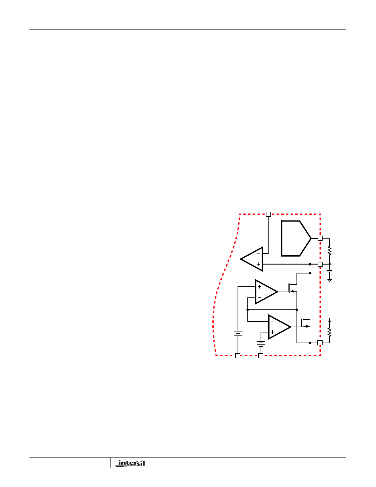
Output-Voltage Offset Programming
The ISL6326B allows the designer to accurately adjust the
offset voltage. When a resistor, R
OFS to VCC, the voltage across it is regulated to 1.6V. This
causes a proportional current (I
R
is connected to ground, the voltage across it is
OFS
regulated to 0.4V, and I
between DAC and REF, R
product (I
OFS
x R
OFS
flows out of OFS. A resistor
OFS
REF
) is equal to the desired offset voltage.
These functions are shown in Figure 6.
Once the desired output offset voltage has been determined,
use the following formulas to set R
For Positive Offset (connect R
1.6 R
×
REF
OFS
------------------------------
=
V
OFFSET
R
For Negative Offset (connect R
0.4 R
×
REF
OFS
------------------------------
=
V
OFFSET
FB
E/A
R
, is connected between
OFS
) to flow into OFS. If
OFS
, is selected so that the
:
OFS
to VCC):
OFS
to GND):
OFS
DYNAMIC
VID D/A
DAC
VCC
GND
(EQ. 11)
(EQ. 12)
R
REF
REF
C
REF
OR
Where V
programmed offset voltage, I
of the converter, R
the ISEN+ pin, and R
active channel number, and R
is the reference voltage, V
REF
LOAD
is the sense resistor connected to
ISEN
is the feedback resistor, N is the
FB
is the
OFS
is the total output current
is the DCR, or R
X
SENSE
depending on the sensing method.
Therefore the equivalent loadline impedance, i.e. Droop
impedance, is equal to:
R
R
FB
------------
R
LL
X
----------------- -=
N
R
ISEN
(EQ. 10)
18
-
1.6V
+
VCC
FIGURE 6. OUTPUT VOLTAGE OFFSET PROGRAMMING
0.4V
+
-
GND
ISL6326B
R
OFS
FN9286.0
April 21, 2006
OFS
Page 19
ISL6326B
Dynamic VID
Modern microprocessors need to make changes to their
core voltage as part of normal operation. They direct the
core-voltage regulator to do this by making changes to the
VID inputs during regulator operation. The power
management solution is required to monitor the DAC inputs
and respond to on-the-fly VID changes in a controlled
manner. Supervising the safe output voltage transition within
the DAC range of the processor without discontinuity or
disruption is a necessary function of the core-voltage
regulator.
In order to ensure the smooth transition of output voltage
during VID change, a VID step change smoothing network,
composed of R
used. The selection of R
voltage as detailed above in Output-Voltage Offset
Programming. The selection of C
duration for 1 bit VID change and the allowable delay time.
Assuming the microprocessor controls the VID change at 1
bit every T
R
REF
VID
and C
equation.
C
REFRREFTVID
REF
and C
as shown in Figure 6, can be
REF
is based on the desired offset
REF
is based on the time
REF
, the relationship between the time constant of
network and T
REF
=
is given by the following
VID
(EQ. 13)
ISL66xx family of Intersil MOSFET drivers, which require
12V bias.
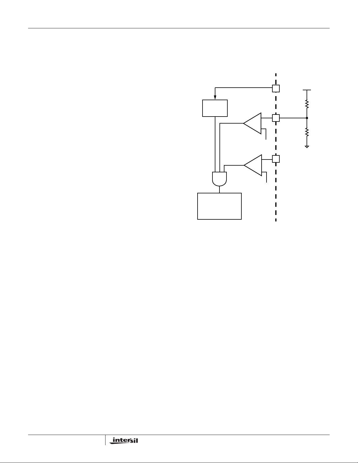
3. The voltage on EN_VTT must be higher than 0.875V to
enable the controller. This pin is typically connected to the
output of VTT VR.
ISL6326B INTERNAL CIRCUIT
POR
CIRCUIT
SOFT-START
AND
FAULT LOGIC
ENABLE
COMPARATOR
+
-
0.875V
+
-
0.875V
EXTERNAL CIRCUIT
VCC
EN_PWR
EN_VTT
+12V
10kΩ
910Ω
Operation Initialization
Prior to converter initialization, proper conditions must exist
on the enable inputs and VCC. When the conditions are met,
the controller begins soft-start. Once the output voltage is
within the proper window of operation, VR_RDY asserts
logic high.
Enable and Disable
While in shutdown mode, the PWM outputs are held in a
high-impedance state to assure the drivers remain off. The
following input conditions must be met before the ISL6326B
is released from shutdown mode.
1. The bias voltage applied at VCC must reach the internal
power-on reset (POR) rising threshold. Once this
threshold is reached, proper operation of all aspects of
the ISL6326B is guaranteed. Hysteresis between the
rising and falling thresholds assure that once enabled,
the ISL6326B will not inadvertently turn off unless the
bias voltage drops substantially (see Electrical
Specifications).
2. The ISL6326B features an enable input (EN_PWR) for
power sequencing between the controller bias voltage
and another voltage rail. The enable comparator holds
the ISL6326B in shutdown until the voltage at EN_PWR
rises above 0.875V. The enable comparator has about
130mV of hysteresis to prevent bounce. It is important
that the driver ICs reach their POR level before the
ISL6326B becomes enabled. The schematic in Figure 7
demonstrates sequencing the ISL6326B with the
FIGURE 7. POWER SEQUENCING USING THRESHOLD-
SENSITIVE ENABLE (EN) FUNCTION
When all conditions above are satisfied, ISL6326B begins
the soft-start and ramps the output voltage to 1.1V first. After
remaining at 1.1V for some time, ISL6326B reads the VID
code at VID input pins. If the VID code is valid, ISL6326B will
regulate the output to the final VID setting. If the VID code is
OFF code, ISL6326B will shut down, and cycling VCC,
EN_PWR or EN_VTT is needed to restart.
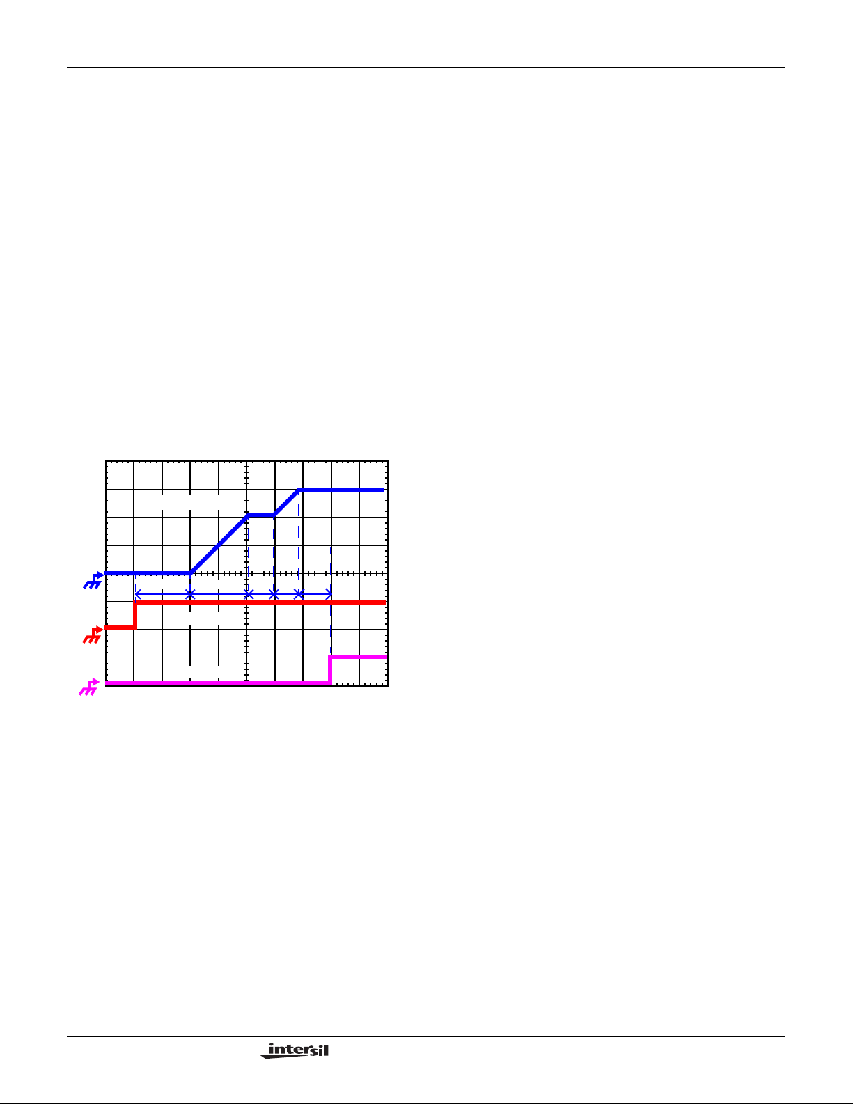
Soft-Start
ISL6326B based VR has 4 periods during soft-start as
shown in Figure 8. After VCC, EN_VTT and EN_PWR reach
their POR/enable thresholds, The controller will have fixed
delay period TD1. After this delay period, the VR will begin
first soft-start ramp until the output voltage reaches 1.1V
Vboot voltage. Then, the controller will regulate the VR
voltage at 1.1V for another fixed period TD3. At the end of
TD3 period, ISL6326B reads the VID signals. If the VID code
is valid, ISL6326B will initiate the second soft-start ramp until
the voltage reaches the VID voltage minus offset voltage.
The soft-start time is the sum of the 4 periods as shown in
the following equation.
T
TD1TD2TD3TD4+++=
SS
TD1 is a fixed delay with the typical value as 1.36ms. TD3 is
determined by the fixed 85µs plus the time to obtain valid
(EQ. 14)
19
FN9286.0
April 21, 2006
Page 20
ISL6326B
VID voltage. If the VID is valid before the output reaches the
1.1V, the minimum time to validate the VID input is 500ns.
Therefore the minimum TD3 is about 86µs.
During TD2 and TD4, ISL6326B digitally controls the DAC
voltage change at 6.25mV per step. The time for each step is
determined by the frequency of the soft-start oscillator which
is defined by the resistor R
from SS pin to GND. The
SS
second soft-start ramp time TD2 and TD4 can be calculated
based on the following equations:
1.1xR
SS
----------------------- -
TD2
TD4
6.25x25
V
------------------------------------------------
For example, when VID is set to 1.5V and the R
VID
6.25x25
μs()=
1.1–()xR
SS
(EQ. 15)
is set at
SS
(EQ. 16)
μs()=
100kΩ, the first soft-start ramp time TD2 will be 704µs and
the se c o nd s oft-st ar t ra m p t i m e T D 4 will be 256µs.
After the DAC voltage reaches the final VID setting,
VR_RDY will be set to high with the fixed delay TD5. The
typical value for TD5 is 85µs.
VOUT, 500mV/DIV
either the DCR of the inductor or R
depending on the
SENSE
sensing method.
The resistor from the IOUT pin to GND should be chosen to
ensure that the voltage at the IOUT pin is less than 2V under
the maximum load current. If the IOUT pin voltage is higher
than 2V, overcurrent shutdown will be triggered, as
described in the Overcurrent Protection section.
A small capacitor can be placed between the IOUT pin and
GND to reduce the noise impact. If this pin is not used, tie it
to GND.
Fault Monitoring and Protection
The ISL6326B actively monitors output voltage and current
to detect fault conditions. Fault monitors trigger protective
measures to prevent damage to a microprocessor load. One
common power good indicator is provided for linking to
external system monitors. The schematic in Figure 9 outline s
the interaction between the fault monitors and the VR_RDY
signal.
VR_RDY Signal
The VR_RDY pin is an open-drain logic output to indicate
that the soft-start period has completed and the output
voltage is within the regulated range. VR_RDY is pulled low
during shutdown and releases high after a successful softstart and a fixed delay TD5. VR_RDY will be pulled low when
an undervoltage or overvoltage condition is detected, or the
controller is disabled by a reset from EN_PWR, EN_VTT,
POR, or VID OFF-code.
TD1
EN_VTT
VR_RDY
FIGURE 8. SOFT-START WAVEFORMS
TD2
500µs/DIV
TD3 TD4
TD5
Current Sense Output
The current flowing out of the IOUT pin is equal to the
sensed average current inside ISL6326B. In typical
application, a resistor is placed from the IOUT pin to GND to
generate a voltage, which is proportional to the load current
and the resistor value:
R
V
IOUT
where V
-------------------
=
IOUT
resistor between the IOUT pin and GND, I
output current of the converter, R
connected to the ISEN+ pin, N is the active channel number,
and R
is the DC resistance of the current sense element,
X
R
IOUT
N
X
----------------- -I
R
ISEN
LOAD
is the voltage at the IOUT pin, R
is the sense resistor
ISEN
LOAD
(EQ. 17)
is the
IOUT
is the total
Undervoltage Detection
The undervoltage threshold is set at 50% of the VID code.
When the output voltage at VSEN is below the undervoltage
threshold, VR_RDY is pulled low.
Overvoltage Protection
Regardless of the VR being enabled or not, the ISL6326B
overvoltage protection (OVP) circuit will be active after its
POR. The OVP thresholds are different under different
operation conditions. When VR is not enabled and during
the soft-start intervals TD1, TD2 and TD3, the OVP
threshold is 1.275V. Once the controller detects valid VID
input, the OVP trip point will be changed to DAC plus
175mV.
Two actions are taken by the ISL6326B to protect the
microprocessor load when an overvoltage condition occurs.
At the inception of an overvoltage event, all PWM outputs
are commanded low instantly (less than 20ns). This causes
the Intersil drivers to turn on the lower MOSFETs and pull
the output voltage below a level to avoid damaging the load.
When the VDIFF voltage falls below the DAC plus 75mV,
PWM signals enter a high-impedance state. The Intersil
drivers respond to the high-impedance input by turning off
both upper and lower MOSFET s. If the overvoltage condition
reoccurs, the ISL6326B will again command the lower
20
FN9286.0
April 21, 2006
Page 21
ISL6326B
MOSFETs to turn on. The ISL6326B will continue to protect
the load in this fashion as long as the overvoltage condition
occurs.
Once an overvoltage condition is detected, normal PWM
operation ceases until the ISL6326B is reset. Cycling the
voltage on EN_PWR, EN_VTT or VCC below the PORfalling threshold will reset the controller. Cycling the VID
codes will not reset the controller.
VR_RDY
UV
-
+
50%
85µA
-
OC
+
I
AVG
2.0V
-
+
IOUT
VDIFF
DAC
SOFT-START, FAULT
AND CONTROL LOGIC
+
OV
-
OC
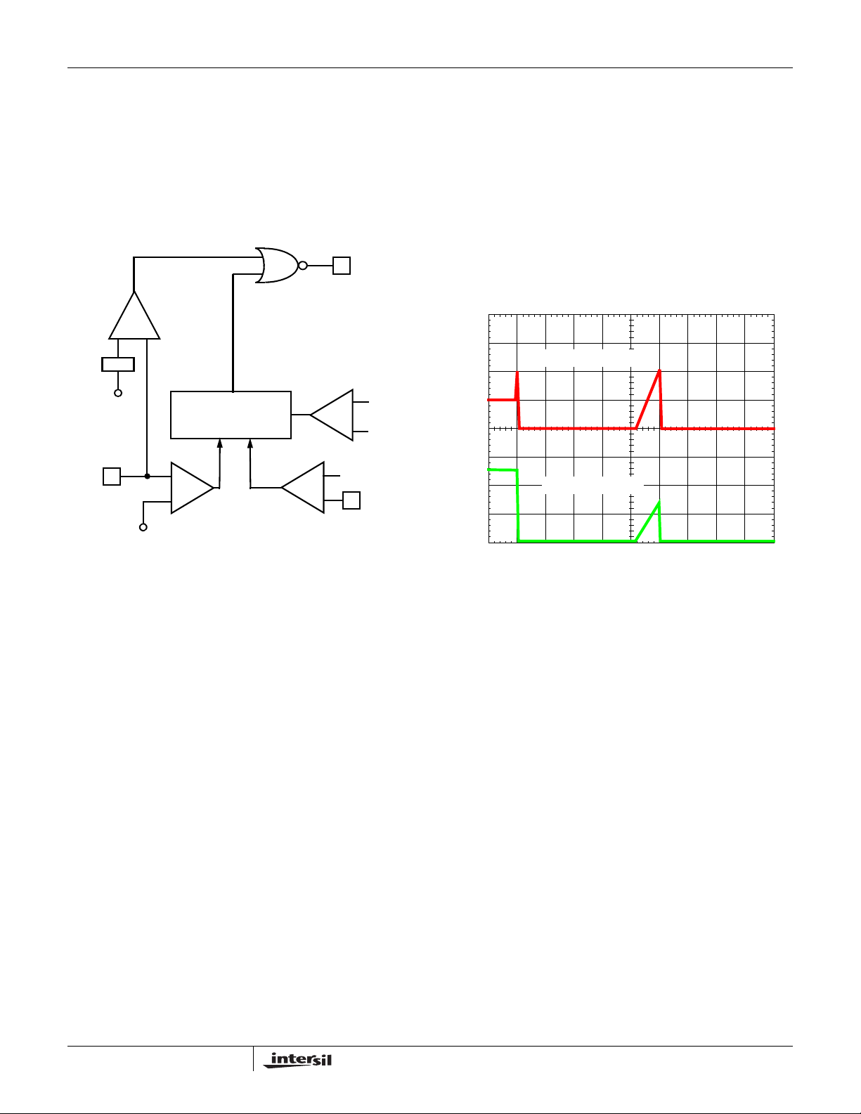
At the beginning of overcurrent shutdown, the controller
places all PWM signals in a high-impedance state within
20ns, commanding the Intersil MOSFET driver ICs to turn off
both upper and lower MOSFETs. The system remains in this
state a period of 4096 switching cycles. If the controller is still
enabled at the end of this wait period, it will attempt a softstart. If the fault remains, the trip-retry cycles will continue
indefinitely (as shown in Figure 10) until either controller is
disabled or the fault is cleared. Note that the energy
delivered during trip-retry cycling is much less than during
full-load operation, so there is no thermal hazard during this
kind of operation.
OUTPUT CURRENT
0A
OUTPUT VOLT AGE
VID + 0.175V
FIGURE 9. VR_RDY AND PROTECTION CIRCUITRY
Overcurrent Protection
ISL6326B has two levels of overcurrent protection. Each
phase is protected from a sustained overcurrent condition by
limiting its peak current, while the combined phase currents
are protected on an instantaneous basis.
In instantaneous protection mode, ISL6326B utilizes the
sensed average current I
condition. See the Channel-Current Balance section for
more detail on how the average current is measured. The
average current is continually compared with a constant
85µA reference current, as shown in Figure 9. Once the
average current exceeds the reference current, a
comparator triggers the converter to shutdown.
The current out of IOUT pin is equal to the sensed average
current I
. With a resistor from IOUT to GND, the voltage
AVG
at IOUT will be proportional to the sensed average current
and the resistor value. ISL6326B continuously monitors the
voltage at IOUT pin. If the voltage at IOUT pin is higher than
2V, a comparator triggers the overcurrent shutdown. By
increasing the resistor between IOUT and GND, the
overcurrent protection threshold can be adjusted to be less
than 100µA. For example, the overcurrent threshold for the
sensed average current I
25k
Ω resistor from IOUT to GND.
to detect an overcurrent
AVG
can be set to 80µA by using a
AVG
0V
FIGURE 10. OVERCURRENT BEHAVIOR IN HICCUP MODE.
F
= 500kHz
SW
2ms/DIV
For the individual channel overcurrent protection, the
ISL6326B continuously compares the sensed current signal
of each channel with the 120µA reference current. If one
channel current exceeds the reference current, ISL6326B
will pull PWM signal of this channel to low for the rest of the
switching cycle. This PWM signal can be turned on next
cycle if the sensed channel current is less than the 120µA
reference current. The peak current limit of individual
channel will not trigger the converter to shutdown.
Thermal Monitoring (VR_HOT/VR_F AN)
There are two thermal signals to indicate the temperature
status of the voltage regulator: VR_HOT and VR_FAN. Both
VR_FAN and VR_HOT pins are open-drain outputs, and
external pull-up resistors are required. Those signals are
valid only after the controller is enabled.
The VR_FAN signal indicates that the temperature of the
voltage regulator is high and more cooling airflow is needed.
The VR_HOT signal can be used to inform the system that
the temperature of the voltage regulator is too high and the
CPU should reduce its power consumption. The VR_HOT
signal may be tied to the CPU’s PROC_HOT signal.
21
FN9286.0
April 21, 2006
Page 22
ISL6326B
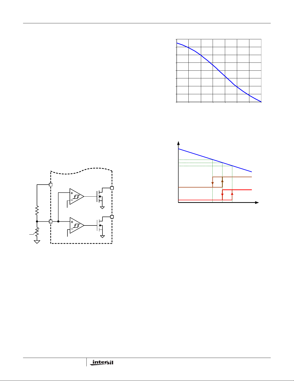
The diagram of thermal monitoring function block is shown in
Figure 11. One NTC resistor should be placed close to the
power stage of the voltage regulator to sense the operational
temperature, and one pull-up resistor is needed to form the
voltage divider for the TM pin. As the temperature of the
power stage increases, the resistance of the NTC will
reduce, resulting in the reduced voltage at the TM pin.
Figure 12 shows the TM voltage over the temperature for a
typical design with a recommended 6.8kΩ NTC (P/N:
NTHS0805N02N6801 from Vishay) and 1kΩ resistor RTM1.
We recommend using those resistors for the accurate
temperature compensation.
There are two comparators with hysteresis to compare the
TM pin voltage to the fixed thresholds for VR_FAN and
VR_HOT signals respectively. The VR_FAN signal is set to
high when the TM voltage is lower than 33% of VCC voltage,
and is pulled to GND when the TM voltage increases to
above 39% of VCC voltage. The VR_FAN signal is set to
high when the TM voltage goes below 28% of VCC voltage,
and is pulled to GND when the TM voltage goes back to
above 33% of VCC voltage. Figure 13 shows the operation
of those signals.
VTM / V
100%
90%
80%
70%
CC
60%
/ V
TM
V
50%
40%
30%
20%
0 20 40 60 80 100 120 140
vs. Temperature
CC
Temperature (
o
C)
FIGURE 12. THE RATIO OF TM VOLTAGE TO NTC
TEMPERATURE WITH RECOMMENDED PARTS
TM
0.39*Vcc
0.33*Vcc
0.28*Vcc
VCC
VR_FAN
R
TM1
TM
o
R
c
NTC
0.33V
0.28V
CC
VR_HOT
CC
FIGURE 11. BLOCK DIAGRAM OF THERMAL MONITORING
FUNCTION
VR_FAN
VR_HOT
T1 T2 T3
Temperature
FIGURE 13. VR_HOT AND VR_FAN SIGNAL vs TM VOLTAGE
Based on the NTC temperature characteristics and the
desired threshold of the VR_HOT signal, the pull-up resistor
RTM1 of TM pin is given by:
R
R
=
TM1
NTC(T3)
2.75xR
NTC T3()
(EQ. 18)
is the NTC resistance at the VR_HOT threshold
temperature T3.
The NTC resistance at the set point T2 and release point T1
of VR_FAN signal can be calculated as:
R
NTC T2()
R
NTC T1()
1.267xR
=
1.644xR
=
NTC T3()
NTC T3()
(EQ. 19)
(EQ. 20)
22
With the NTC resistance value obtained from Equations 19
and 20, the temperature value T2 and T1 can be found from
the NTC datasheet.
FN9286.0
April 21, 2006
Page 23
ISL6326B
Temperature Compensation
ISL6326B supports inductor DCR sensing, or resistive
sensing techniques. The inductor DCR has a positive
temperature coefficient, which is about +0.38%/°C. Since the
voltage across inductor is sensed for the output current
information, the sensed current has the same positive
temperature coefficient as the inductor DCR.
In order to obtain the correct current information, there
should be a way to correct the temperature impact on the
current sense component. ISL6326B provides two methods:
integrated temperature compensation and external
temperature compensation.
Integrated Temperature Compensation
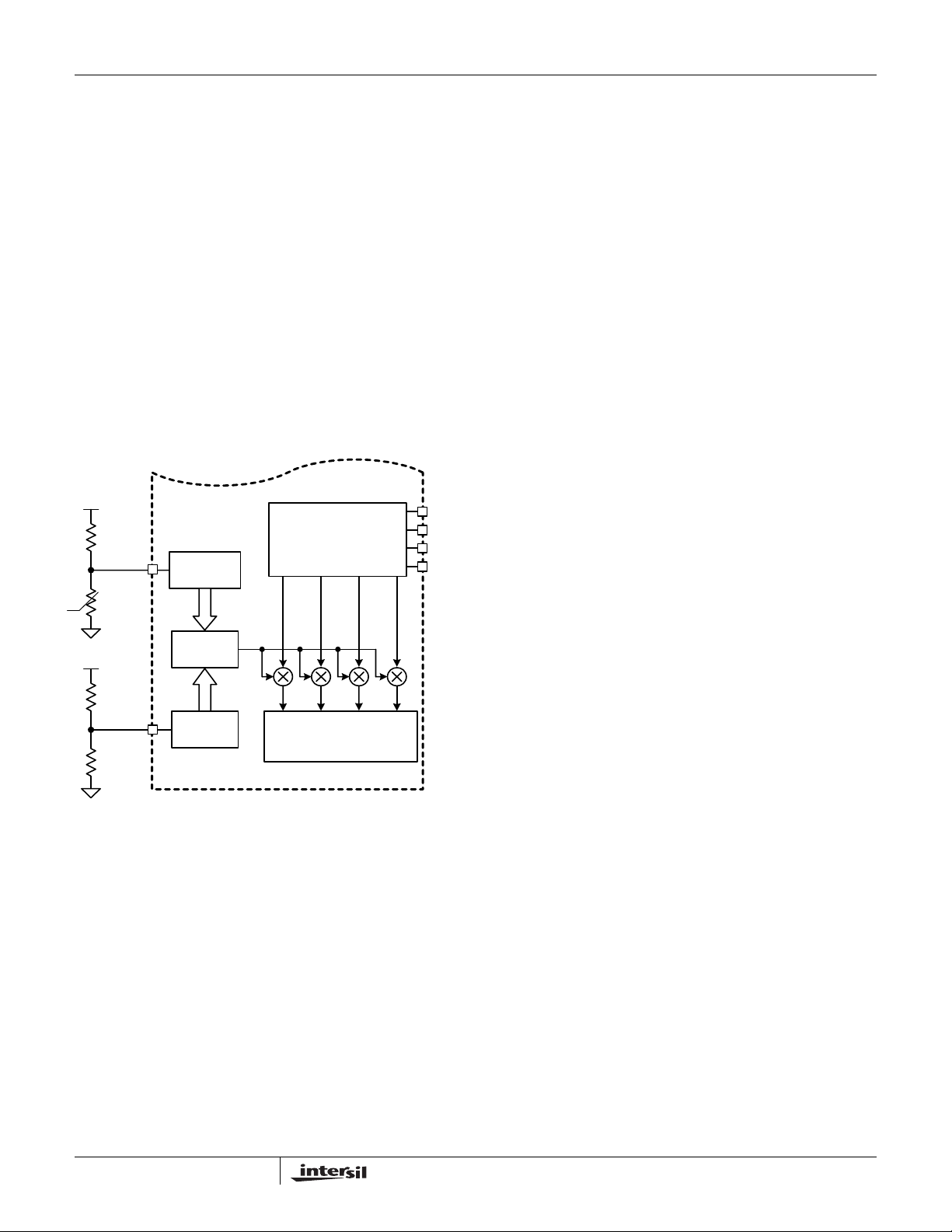
When the TCOMP voltage is equal or greater than VCC/15,
ISL6326B will utilize the voltage at TM and TCOMP pins to
compensate the temperature impact on the sensed current.
The block diagram of this function is shown in Figure 14.
V
CC
R
TM1
TM
o
R
c
NTC
V
CC
R
TC1
TCOMP
R
TC2
FIGURE 14. BLOCK DIAGRAM OF INTEGRATED
Non-linear
A/D
D/A
4-bit
A/D
TEMPERATURE COMPENSATION
When the TM NTC is placed close to the current sense
component (inductor), the temperature of the NTC will track
the temperature of the current sense component. Therefore
the TM voltage can be utilized to obtain the temperature of
the current sense component.
Based on VCC voltage, ISL6326B converts the TM pin
voltage to a 6-bit TM digital signal for temperature
compensation. With the non-linear A/D converter of
ISL6326B, the TM digital signal is linearly proportional to the
NTC temperature. For accurate temperature compensation,
the ratio of the TM voltage to the NTC temperature of the
practical design should be similar to that in Figure 12.
Depending on the location of the NTC and the airflow, the
NTC may be cooler or hotter than the current sense
Channel current
sense
I
I
3
4
k
i
Droop &
Over current protection
I
I
1
2
I
sen4
I
sen3
I
sen2
I
sen1
component. The TCOMP pin voltage can be utilized to
correct the temperature difference between NTC and the
current sense component. When a different NTC type or
different voltage divider is used for the TM function, the
TCOMP voltage can also be used to compensate for the
difference between the recommended TM voltage curve in
Figure 13 and that of the actual design. According to the
VCC voltage, ISL6326B converts the TCOMP pin voltage to
a 4-bit TCOMP digital signal as TCOMP factor N.
The TCOMP factor N is an integer between 0 and 15. The
integrated temperature compensation function is disabled for
N = 0. For N = 4, the NTC temperature is equal to the
temperature of the current sense component. For N < 4, the
NTC is hotter than the current sense component. The NTC is
cooler than the current sense component for N > 4. When
N > 4, the larger TCOMP factor N, the larger the difference
between the NTC temperature and the temperature of the
current sense component.
ISL6326B multiplexes the TCOMP factor N with the TM
digital signal to obtain the adjustment gain to compensate
the temperature impact on the sensed channel current. The
compensated channel current signal is used for droop and
overcurrent protection functions.
Design Procedure
1. Properly choose the voltage divider for the TM pin to
match the TM voltage vs temperature curve with the
recommended curve in Figure 12.
2. Run the actual board under the full load and the desired
cooling condition.
3. After the board reaches the thermal steady state, record
the temperature (T
(inductor or MOSFET) and the voltage at TM and VCC
pins.
4. Use the following equation to calculate the resistance of
the TM NTC, and find out the corresponding NTC
temperature T
R
NTC T
()
NTC
NTC
VTMxR
------------------------------- -=
5. Use the following equation to calculate th e TCOMP
factor N:
()
209x T
CSC
--------------------------------------------------------
N
3xT
NTC
6. Choose an integral number close to the above result for
the TCOMP factor. If this factor is higher than 15, use
N = 15. If it is less than 1, use N = 1.
7. Choose the pull-up resistor R
8. If N = 15, do not need the pull-down resistor R
otherwise obtain R
NxR
TC1
TC2
-----------------------
=
15 N–
R
9. Run the actual board under full load again with the proper
resistors connected to the TCOMP pin.
) of the current sense component
CSC
from the NTC datasheet.
TM1
VCCV–
TM
T–
NTC
400+
4+=
(typical 10kΩ);
TC1
by the following equation:
TC2
(EQ. 21)
(EQ. 22)
TC2
(EQ. 23)
,
23
FN9286.0
April 21, 2006
Page 24
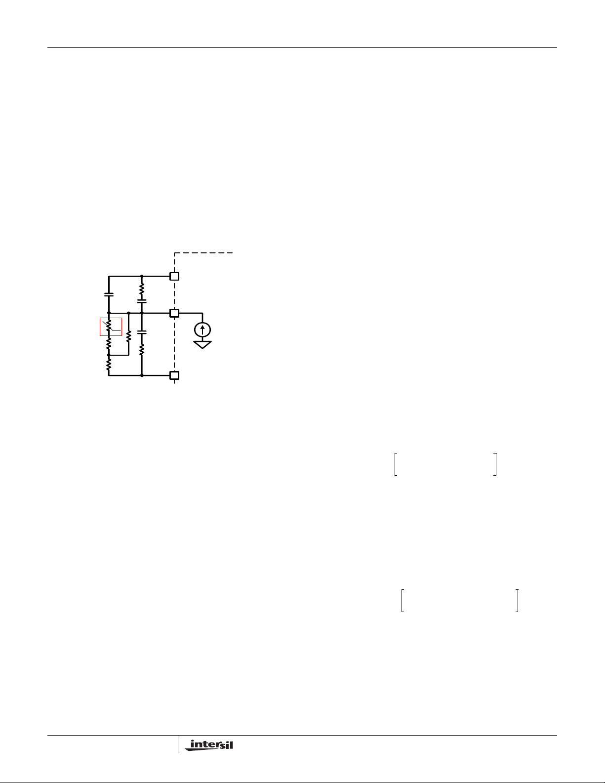
ISL6326B
10. Record the output voltage as V1 immediately after the
output voltage is stable with the full load. Record the
output voltage as V2 after the VR reaches the thermal
steady state.
11. If the output voltage increases over 2mV as the
temperature increases, i.e. V2-V1 > 2mV, reduce N and
redesign R
; if the output voltage decreases over 2mV
TC2
as the temperature increases, i.e. V1-V2 > 2mV , increase
N and redesign R
TC2
.
External Temperature Compensation
By pulling the TCOMP pin to GND, the integrated
temperature compensation function is disabled. And one
external temperature compensation network, shown in
Figure 15, can be used to cancel the temperature impact on
the droop (i.e., load line).
ISL6326B
COMP
o
C
Interna l
circuit
FB
ISEN
Power Stages
The first step in designing a multiphase converter is to
determine the number of phases. This determination
depends heavily on the cost analysis which in turn depends
on system constraints that differ from one design to the next.
Principally, the designer will be concerned with whether
components can be mounted on both sides of the circuit
board; whether through-hole components are permitted; and
the total board space available for power-supply circuitry.
Generally speaking, the most economical solutions are
those in which each phase handles between 15 and 20A. All
surface-mount designs will tend toward the lower end of this
current range. If through-hole MOSFETs and inductors can
be used, higher per-phase currents are possible. In cases
where board space is the limiting constraint, current can be
pushed as high as 40A per phase, but these designs require
heat sinks and forced air to cool the MOSFETs, inductors
and heat-dissipating surfaces.
MOSFETs
The choice of MOSFETs depends on the current each
MOSFET will be required to conduct; the switching
frequency; the capability of the MOSFETs to dissipate heat;
and the availability and nature of heat sinking and air flow.
VDIFF
FIGURE 15. EXTERNAL TEMPERATURE COMPENSATION
The sensed current will flow out of the FB pin and develop a
droop voltage across the resistor equivalent (R
the FB and VDIFF pins. If R
resistance reduces as the
FB
) between
FB
temperature increases, the temperature impact on the droop
can be compensated. An NTC resistor can be placed close
to the power stage and used to form R
. Due to the
FB
non-linear temperature characteristics of the NTC, a resistor
network is needed to make the equivalent resistance
between the FB and VDIFF pins reverse proportional to the
temperature.
The external temperature compensation network can only
compensate the temperature im pact on the droop, while it
has no impact to the sensed current inside ISL6326B.
Therefore, this network cannot compensate for the
temperature impact on the overcurrent protection function.
General Design Guide
This design guide is intended to provide a high-level
explanation of the steps necessary to create a multiphase
power converter. It i s assume d that the reader is familiar with
many of the basic skills and techniques referenced below. In
addition to this guide, Intersil provides complete reference
designs that include schematics, bills of materials, and
example board layouts for all common microprocessor
applications.
LOWER MOSFET POWER CALCULATION
The calculation for heat dissipated in the lower MOSFET is
simple, since virtually all of the heat loss in the lower
MOSFET is due to current conducted through the channel
resistance (R
continuous output current; I
current (see Equation 1); d is the duty cycle (V
). In Equation 24, IM is the maximum
DS(ON)
is the peak-to-peak inductor
PP
OUT/VIN
); and
L is the per-channel inductance.
P
LOW 1,
r
DS ON()
⎛⎞
I
M
⎜⎟
----- N
⎝⎠
2
1d–()
I
LPP,
--------------------------------+=
2
1d–()
12
(EQ. 24)
An additional term can be added to the lower-MOSFET loss
equation to account for additional loss accrued during the
dead time when inductor current is flowing through the
lower-MOSFET body diode. This term is dependent on the
diode forward voltage at I
frequency, f
; and the length of dead times, td1 and td2, at
S
, V
M
; the switching
D(ON)
the beginning and the end of the lower-MOSFET conduction
interval respectively .
P
LOW 2,
=
V
DON()fS
I
I
⎛⎞
M
PP
----- -
-------- -+
⎝⎠
N
2
⎛⎞
I
M
t
⎜⎟
+
----- -
d1
N
⎝⎠
I
PP
-------- -
–
2
(EQ. 25)
t
d2
Thus the total maximum power dissipated in each lower
MOSFET is approximated by the summation of P
P
LOW,2
.
LOW,1
and
Upper MOSFET Power Calculation
In addition to R
losses, a large portion of the upper-
DS(ON)
MOSFET losses are due to currents conducted across the
input voltage (V
) during switching. Since a substantially
IN
24
FN9286.0
April 21, 2006
Page 25

ISL6326B
higher portion of the upper-MOSFET losses are dependent
on switching frequency, the power calculation is more
complex. Upper MOSFET losses can be divided into
separate components involving the upper-MOSFET
switching times; the lower-MOSFET body-diode reverserecovery charge, Q
; and the upper MOSFET R
rr
DS(ON)
conduction loss.
When the upper MOSFET turns off, the lower MOSFET does
not conduct any portion of the inductor current until the
voltage at the phase node falls below ground. Once the
lower MOSFET begins conducting, the current in the upper
MOSFET falls to zero as the current in the lower MOSFET
ramps up to assume the full inductor current. In Equation 26,
the required time for this commutation is t
approximated associated power loss is P
P
≈
UP 1,VIN
I
M
⎛⎞
----- -
⎝⎠
N
t
I
⎛⎞
1
PP
-------- -+
2
----
⎜⎟
2
⎝⎠
f
S
and the
1
.
UP,1
(EQ. 26)
At turn on, the upper MOSFET begins to conduct and this
transition occurs over a time t2. In Equation 27, the
approximate power loss is P
t
I
≈
P
UP 2,VIN
⎛⎞
I
M
⎜⎟
----- N
⎝⎠
⎛⎞
PP
2
-------- -
----
⎜⎟
–
2
2
⎝⎠
.
UP,2
f
S
(EQ. 27)
A third component involves the lower MOSFET’s reverserecovery charge, Qrr. Since the inductor current has fully
commutated to the upper MOSFET before the lowerMOSFET’s body diode can draw all of Q
, it is conducted
rr
through the upper MOSFET across VIN. The power
dissipated as a result is P
VINQrrf
=
P
UP 3,
S
and is approximately
UP,3
(EQ. 28)
Finally, the resistive part of the upper MOSFET’s is given in
Equation 29 as P
UP,4
.
The total power dissipated by the upper MOSFET at full load
can now be approximated as the summa ti on of the resu l ts
from Equations 26, 27, and 28. Since the power equations
depend on MOSFET parameters, choosing the correct
MOSFETs can be an iterative process involving repetitive
solutions to the loss equations for different MOSFETs and
different switching frequencies.
2
2
P
UP 4,rDS ON()
⎛⎞
I
⎜⎟
----- -
⎝⎠
I
M
N
PP
d+≈
d
---------12
(EQ. 29)
Current Sensing Resistor
The resistors connected to the Isen+ pins determine the
gains in the load-line regulation loop and the channel-current
balance loop as well as setting the overcurrent trip point.
Select values for these resistors by the following equation:
R
I
X
R
ISEN
----------------------85 10
×
OCP
------------- -=
–
6
N
(EQ. 30)
where R
pin, N is the active channel number, R
is the sense resistor connected to the ISEN+
ISEN
is the resistance of
X
the current sense element, either the DCR of the inductor or
R
desired overcurrent trip point. Typically, I
depending on the sensing method, and I
SENSE
can be chosen
OCP
OCP
is the
to be 1.3 times the maximum load current of the specific
application.
With integrated temperature compensation, the sensed
current signal is independent on the operational temperature
of the power stage, i.e. the temperature effect on the current
sense element R
temperature compensation function. R
is cancelled by the integrated
X
in Equation 30
X
should be the resistance of the current sense element at the
room temperature.
When the integrated temperature compensation function is
disabled by pulling the TCOMP pin to GND, the sensed
current will be dependent on the operational temperature of
the power stage, since the DC resistance of the current
sense element may be changed according to the operational
temperature. R
in Equation 30 should be the maximum DC
X
resistance of the current sense element at the all operational
temperature.
In certain circumstances, it may be necessary to adjust the
value of one or more ISEN resistors. When the components
of one or more channels are inhibited from effectively
dissipating their heat so that the affected channels run hotter
than desired, choose new, smaller values of RISEN for the
affected phases (see the section entitled Channel-Current
Balance). Choose R
in proportion to the desired
ISEN,2
decrease in temperature rise in order to cause proportionally
less current to flow in the hotter phase:
ΔT
R
ISEN 2,
R
ISEN
In Equation 31, make sure that ΔT
----------=
ΔT
2
1
is the desired temperature
2
rise above the ambient temperature, and ΔT
is the measured
1
(EQ. 31)
temperature rise above the ambient temperature. While a
single adjustment according to Equation 31 is usually
sufficient, it may occasionally be necessary to adjust R
ISEN
two or more times to achieve optimal thermal balance
between all channels.
Load-Line Regulation Resistor
The load-line regulation resistor is labelled RFB in Figure 5.
Its value depends on the desired loadline requirement of the
application.
The desired loadline can be calculated by the following
equation:
V
DROOP
------------------------ -=
R
LL
where I
and VR
I
FL
is the full load current of the specific application,
FL
DROOP
load condition.
is the desired voltage droop under the full
(EQ. 32)
25
FN9286.0
April 21, 2006
Page 26
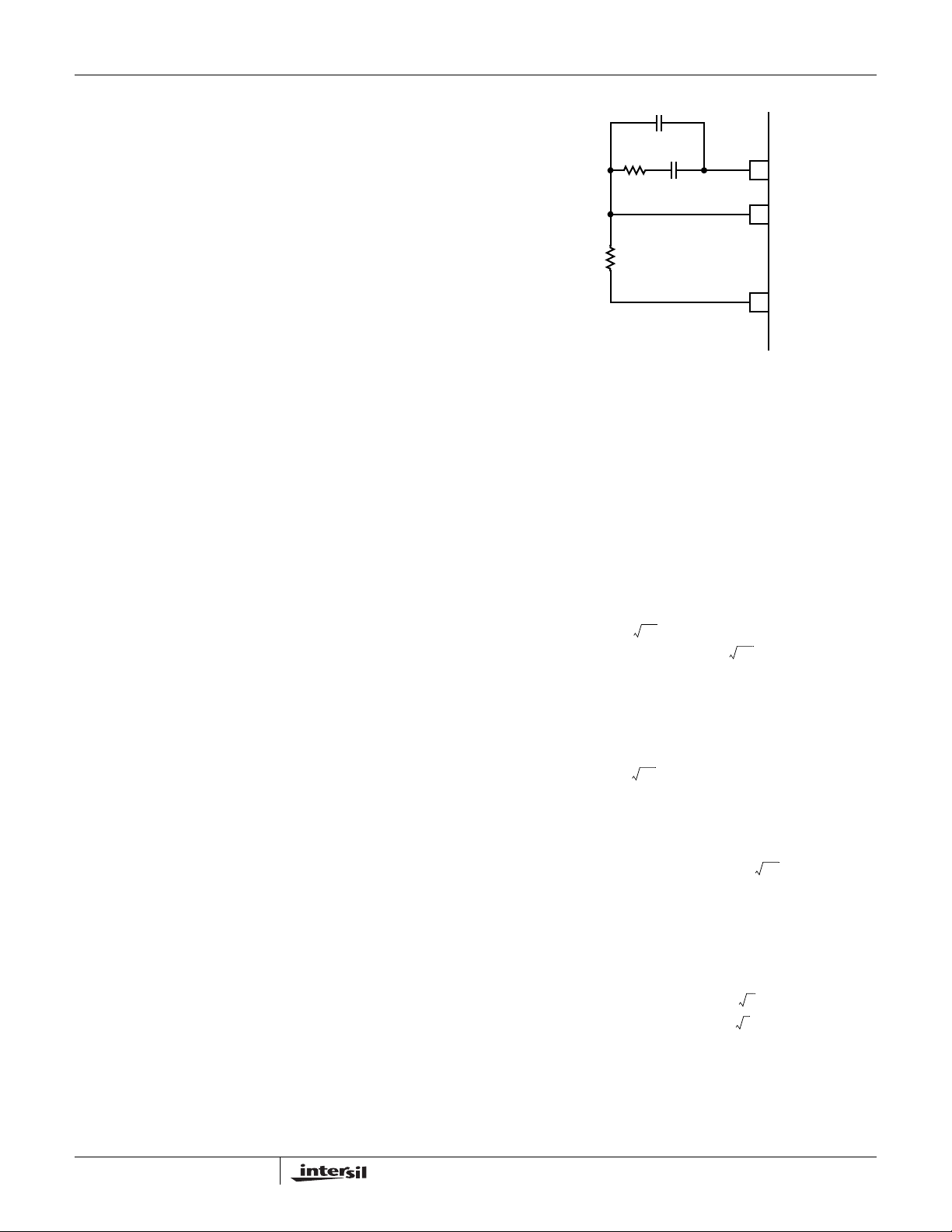
ISL6326B
Based on the desired loadline RLL, the loadline regulation
resistor can be calculated by the following equation:
N
R
--------------------------------- -=
FB
where N is the active channel number, R
resistor connected to the ISEN+ pin, and R
R
ISEN
R
R
LL
X
ISEN
is the
X
(EQ. 33)
is the sense
resistance of the current sense element, either the DCR of
the inductor or R
SENSE
depending on the sensing method.
If one or more of the current sense resistors are adjusted for
thermal balance, as in Equation 31, the load-line regulation
resistor should be selected based on the average value of
the current sensing resistors, as given in the following
equation:
R
LL
---------- R
=
R
FB
where R
∑
R
X
ISEN(n)
ISEN n()
n
is the current sensing resistor connected to
(EQ. 34)
the nth ISEN+ pin.
Compensation
The two opposing goals of compensating the voltage
regulator are stability and speed. Depending on whether the
regulator employs the optional load-line regulation as
described in Load-Line Regulation, there are two distinct
methods for achieving these goals.
COMPENSATING LOAD-LINE REGULATED
CONVERTER
The load-line regulated converter behaves in a similar
manner to a peak-current mode controller because the two
poles at the output-filter L-C resonant frequency split with
the introduction of current information into the control loop.
The final location of these poles is determined by the system
function, the gain of the current signal, and the value of the
compensation components, R
Since the system poles and zero are affected by the values
of the components that are meant to compensate them, the
solution to the system equation becomes fairly complicated.
Fortunately there is a simple approximation that comes very
close to an optimal solution. Treating the system as though it
were a voltage-mode regulator by compensating the L-C
poles and the ESR zero of the voltage-mode approximation
yields a solution that is always stable with very close to ideal
transient performance.
and CC.
C
C2 (OPTIONAL)
C
C
R
C
+
R
FB
V
DROOP
-
FIGURE 16. COMPENSATION CONFIGURATION FOR
The feedback resistor, R
LOAD-LINE REGULATED ISL6326B CIRCUIT
FB
COMP
FB
ISL6326B
VDIFF
, has already been chosen as
outlined in Load-Line Regulation Resistor. Select a target
bandwidth for the compensated system, f
. The target
0
bandwidth must be large enough to assure adequate
transient performance, but smaller than 1/ 3 of the
per-channel switching frequency. The values of the
compensation components depend on the relationships of f
to the L-C pole frequency and the ESR zero frequency. For
each of the three cases which follow, there is a separate set
of equations for the compensation components.
1
------------------- f
Case 1:
Case 2:
Case 3:
------------------2π LC
R
C
f
R
C
>
2π LC
R
CRFB
C
C
CRFB
C
0
CRFB
C
0
0.75V
------------------------------------=
2π VPPRFBf
1
f
0
-------------------------------------------------------------=
2π()2f
1
------------------------------>
2π C ESR()
0.75VINESR()C
-------------------------------------------------=
2π V
2π f0VppLC
----------------------------------- -=
0.75V
IN
IN
0
1
------------------------------<≤
2π C ESR()
VPP2π()2f
--------------------------------------------=
0.75 V
IN
0.75V
IN
2
VPPRFBLC
0
2π f0VppL
------------------------------------------=
0.75 V
PPRFBf0
ESR()
IN
2
LC
0
L
(EQ. 35)
0
26
In Equation 35, L is the per-channel filter inductance divided
by the number of active channels; C is the sum total of all
output capacitors; ESR is the equivalent-series resistance of
FN9286.0
April 21, 2006
Page 27

ISL6326B
the bulk output-filter capacitance; and VPP is the sawtooth
amplitude described in Electrical Specifications.
The optional capacitor C
, is sometimes needed to bypass
2
noise away from the PWM comparator. Keep a position
available for C
, and be prepared to install a high-frequency
2
capacitor of between 22pF and 150pF in case any leadingedge jitter problem is noted.
Once selected, the compensation values in Equation 35
assure a stable converter with reasonable transient
performance. In most cases, transient performance can be
improved by making adjustments to R
value of R
while observing the transient performance on an
C
. Slowly increase the
C
oscilloscope until no further improvement is noted. Normally,
C
will not need adjustment. Keep the value of CC from
C
Equation 35 unless some performance issue is noted.
Output Filter Design
The output inductors and the output capacitor bank together
to form a low-pass filter responsible for smoothing the
pulsating voltage at the phase nodes. The output filter also
must provide the transient energy until the regulator can
respond. Because it has a low bandwidth compared to the
switching frequency, the output filter necessarily limits the
system transient response. The output capacitor must
supply or sink load current while the current in the output
inductors increases or decreases to meet the dema n d.
In high-speed converters, the output capacitor bank is
usually the most costly (and often the largest) part of the
circuit. Output filter design begins with minimizing the cost of
this part of the circuit. The critical load parameters in
choosing the output capacitors are the maximum size of the
load step, ΔI; the load-current slew rate, di/dt; and the
maximum allowable output-voltage deviation under transient
loading, ΔV
their capacitance, ESR, and ESL (equivalent series
inductance).
At the beginning of the load transient, the output capacitors
supply all of the transient current. The output voltage will
initially deviate by an amount approximated by the voltage
drop across the ESL. As the load current increases, the
voltage drop across the ESR increases linearly until the load
current reaches its final value. The capacitors selected must
have sufficiently low ESL and ESR so that the total outputvoltage deviation is less than the allowable maximum.
Neglecting the contribution of inductor current and regulator
response, the output voltage initially deviates by an amount:
ΔV ESL()
The filter capacitor must have sufficiently low ESL and ESR
so that ΔV < ΔV
Most capacitor solutions rely on a mixture of high-frequency
capacitors with relatively low capacitance in combination
. Capacitors are characterized according to
MAX
di
-----ESR()ΔI+≈
dt
.
MAX
(EQ. 36)
with bulk capacitors having high capacitance but limited
high-frequency performance. Minimizing the ESL of the
high-frequency capacitors allows them to support the output
voltage as the current increases. Minimizing the ESR of the
bulk capacitors allows them to supply the increased current
with less output voltage deviation.
The ESR of the bulk capacitors also creates the majority of
the output-voltage ripple. As the bulk capacitors sink and
source the inductor AC ripple current (see Interleaving and
Equation 2), a voltage develops across the bulk-capacitor
ESR equal to I
(ESR). Thus, once the output capacitors
C,PP
are selected, the maximum allowable ripple voltage,
V
PP(MAX)
L ESR()
, determines the lower limit on the inductance.
⎛⎞
NV
–
V
IN
⎝⎠
------------------------------------------------------------≥
fSVINV
V
OUT
OUT
PP MAX()
(EQ. 37)
Since the capacitors are supplying a decreasing portion of
the load current while the regulator recovers from the
transient, the capacitor voltage becomes slightly depleted.
The output inductors must be capable of assuming the entire
load current before the output voltage decreases more than
ΔV
. This places an upper limit on inductance.
MAX
Equation 38 gives the upper limit on L for the cases when
the trailing edge of the current transient causes a greater
output-voltage deviation than the leading edge. Equation 39
addresses the leading edge. Normally, the trailing edge
dictates the selection of L because duty cycles are usually
less than 50%. Nevertheless, both inequalities should be
evaluated, and L should be selected based on the lower of
the two results. In each equation, L is the per-channel
inductance, C is the total output capacitance, and N is the
number of active channels.
2NCV
L
--------------------- ΔV
()
ΔI
()
1.25
------------------------- - ΔV
≤
L
()
ΔI
2
O
NC
2
MAX
MAX
ΔI ESR()–≤
ΔIESR()– VINVO–
⎛⎞
⎝⎠
(EQ. 38)
(EQ. 39)
Input Supply Voltage Selection
The VCC input of the ISL6326B can be connected either
directly to a +5V supply or through a current limiting resistor
to a +12V supply. An integrated 5.8V shunt regulator
maintains the voltage on the VCC pin when a +12V supply is
used. A 300Ω resistor is suggested for limiting the current
into the VCC pin to a worst-case maximum of approximately
25mA.
Switching Frequency Selection
There are a number of variables to consider when choosing
the switching frequency, as there are considerable effects on
the upper-MOSFET loss calculation. These effects are
outlined in MOSFETs, and they establish the upper limit for
the switching frequency. The lower limit is established by the
requirement for fast transient response and small output-
27
FN9286.0
April 21, 2006
Page 28
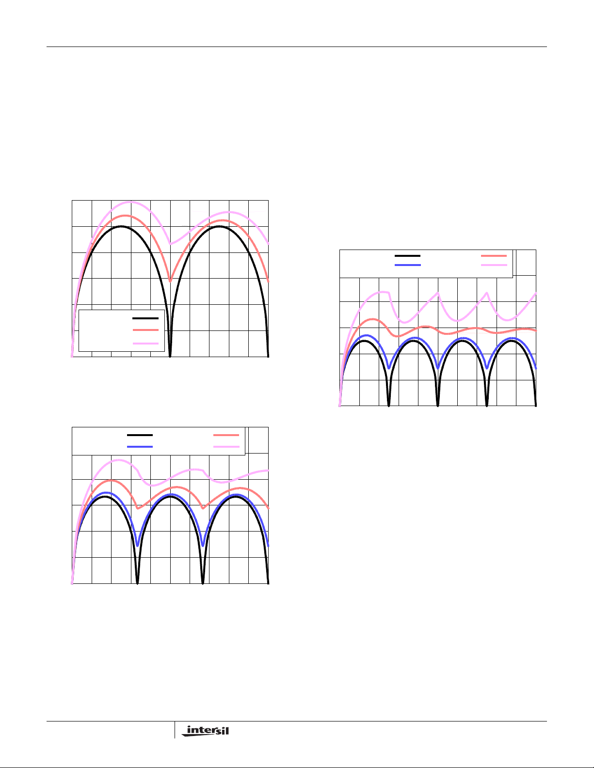
ISL6326B
voltage ripple as outlined in Output Filter Design. Choose the
lowest switching frequency that allows the regulator to meet
the transient-response requirements.
Input Capacitor Selection
The input capacitors are responsible for sourcing the AC
component of the input current flowing into the upper
MOSFETs. Their RMS current capacity must be sufficient to
handle the AC component of the current drawn by the upper
MOSFETs which is related to duty cycle and the number of
active phases.
0.3
)
O
/I
RMS
0.2
0.1
I
= 0
L,PP
= 0.5 I
I
L,PP
I
INPUT-CAPACITOR CURRENT (I
L,PP
0
00.4 1.00.2 0.6 0.8
FIGURE 17. NORMALIZED INPUT -CAP ACITOR RMS CURRENT
0.3
I
L,PP
)
I
L,PP
O
I
RMS/
0.2
0.1
INPUT-CAPACITOR CURRENT (I
0
00.4 1.00.2 0.6 0.8
FIGURE 18. NORMALIZED INPUT -CAP ACITOR RMS CURRENT
O
= 0.75 I
O
DUTY CYCLE (V
O/VIN
)
vs DUTY CYCLE FOR 2-PHASE CONVERTER
= 0
= 0.25 I
O
I
= 0.5 I
L,PP
I
L,PP
DUTY CYCLE (VO/VIN)
O
= 0.75 I
O
vs DUTY CYCLE FOR 3-PHASE CONVERTER
support the RMS current calculated. The voltage rating of
the capacitors should also be at least 1.25 times greater
than the maximum input voltage.
Figures 18 and 19 provide the same input RMS current
information for three and four phase designs respectively.
Use the same approach to selecting the bulk capacitor type
and number as described above.
Low capacitance, high-frequency ceramic capacitors are
needed in addition to the bulk capacitors to suppress leading
and falling edge voltage spikes. The result from the high
current slew rates produced by the upper MOSFETs turn on
and off. Select low ESL ceramic capacitors and place one as
close as possible to each upper MOSFET drain to minimize
board parasitic impedances and maximize suppression.
0.3
I
= 0
L,PP
I
)
O
I
RMS/
0.2
0.1
INPUT-CAPACITOR CURRENT (I
= 0.25 I
L,PP
0
00.4 1.00.2 0.6 0.8
O
I
= 0.5 I
L,PP
I
= 0.75 I
L,PP
DUTY CYCLE (V
O/VIN
O
O
)
FIGURE 19. NORMALIZED INPUT- CAP ACITOR RMS CURRENT
vs DUTY CYCLE FOR 4-PHASE CONVERTER
MULTIPHASE RMS IMPROVEMENT
Figure 20 is provided as a reference to demonstrate the
dramatic reductions in input-capacitor RMS current upon the
implementation of the multiphase topology. For example,
compare the input RMS current requirements of a two-phase
converter versus that of a single phase. Assume both
converters have a duty cycle of 0.25, maximum sustained
output current of 40A, and a ratio of I
to IO of 0.5. The
L,PP
single phase converter would require 17.3Arms current
capacity while the two-phase converter would only require
10.9Arms. The advantages become even more pronounced
when output current is increased and additional phases are
added to keep the component cost down relative to the
single phase approach.
For a two phase design, use Figure 17 to determine the
input-capacitor RMS current requirement given the duty
cycle, maximum sustained output current (I
of the per-phase peak-to-peak inductor current (I
), and the ratio
O
L,PP
) to IO.
Select a bulk capacitor with a ripple current rating which will
minimize the total number of input capacitors required to
28
FN9286.0
April 21, 2006
Page 29
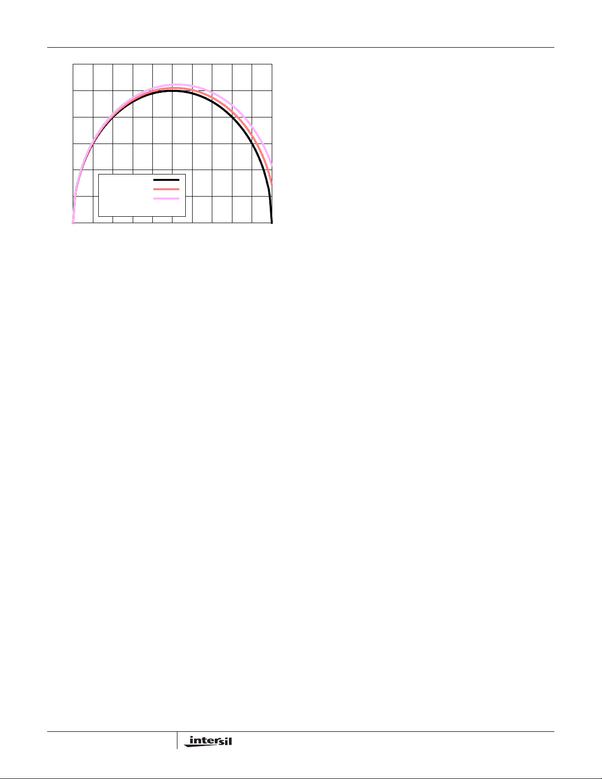
ISL6326B
0.6
)
O
I
RMS/
0.4
0.2
I
= 0
L,PP
I
= 0.5 I
L,PP
I
INPUT-CAPACITOR CURRENT (I
0
00.4 1.00.2 0.6 0.8
FIGURE 20. NORMALIZED INPUT-CAP ACITOR RMS
L,PP
CURRENT vs DUTY CYCLE FOR SINGLE-PHASE
CONVERTER
O
= 0.75 I
DUTY CYCLE (V
O
)
O/VIN
Layout Considerations
The following layout strategies are intended to minimize the
impact of board parasitic impedances on con verter
performance and to optimize the heat-dissipating capabili ties
of the printed-circuit board. These sections highlight some
important practices which should not be overlooked during the
layout process.
Component Placement
Within the allotted implementation area, orient the switching
components first. The switching components are the most
critical because they carry large amounts of energy and tend
to generate high levels of noise. Switching component
placement should take into account power dissipation. Align
the output inductors and MOSFET s such that space between
the components is minimized while creating the PHASE
plane. Place the Intersil MOSFET driver IC as close as
possible to the MOSFET s they control to reduce the parasitic
impedances due to trace length between critical driver input
and output signals. If possible, duplicate the same
placement of these components for each phase.
Next, place the input and output capacitors. Position one
high-frequency ceramic input capacitor next to each upper
MOSFET drain. Place the bulk input capacitors as close to
the upper MOSFET drains as dictated by the component
size and dimensions. Long distances between input
capacitors and MOSFET drains result in too much trace
inductance and a reduction in capacitor performance. Locate
the output capacitors between the inductors and the load,
while keeping them in close proximity to the microprocessor
socket.
29
FN9286.0
April 21, 2006
Page 30
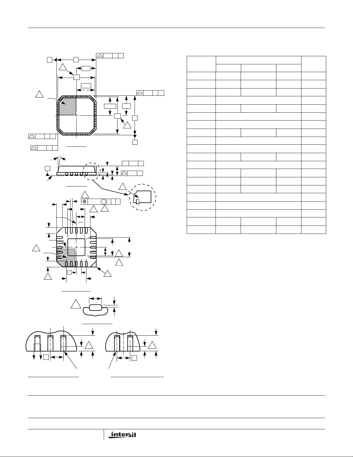
ISL6326B
Quad Flat No-Lead Plastic Package (QFN)
Micro Lead Frame Plastic Package (MLFP)
2X
0.15
C
E1/2 E/2
E1
A2
A
A1
8
E2
7
8
9
CORNER
OPTION 4X
A1
A
9
/ /
0.08
9
(Ne-1)Xe
REF.
E
B
0.10 C
0.152XB
C
C
A
6
INDEX
AREA
AREA
2X
2X
SEATING PLANE
(DATUM B)
(DATUM A)
6
INDEX
AREA
0.15
C
4X
C
4X P
4X P
NX L
1
2
3
B
AC0.15
0
8
D
9
N
BOTTOM VIEW
D1
D1/2
N
TOP VIEW
SIDE VIEW
NX b
D2
D2
2
e
(Nd-1)Xe
REF.
NX b
5
D/2
5
0.10 BAMC
7
NX k
N
1
2
3
A3
E2/2
L40.6x6
40 LEAD QUAD FLAT NO-LEAD PLASTIC PACKAGE
(COMPLIANT TO JEDEC MO-220VJJD-2 ISSUE C)
MILLIMETERS
SYMBOL
A 0.80 0.90 1.00 -
A1 - - 0.05 -
A2 - - 1.00 9
A3 0.20 REF 9
b 0.18 0.23 0.30 5, 8
D 6.00 BSC -
D1 5.75 BSC 9
D2 3.95 4.10 4.25 7, 8
E 6.00 BSC -
E1 5.75 BSC 9
E2 3.95 4.10 4.25 7, 8
e 0.50 BSC -
k0.25 - - -
L 0.30 0.40 0.50 8
L1 - - 0.15 10
N402
Nd 10 3
Ne 10 3
P- -0.609
θ --129
NOTES:
1. Dimensioning and tolerancing conform to ASME Y14.5-1994.
2. N is the number of terminals.
3. Nd and Ne refer to the number of terminals on each D and E.
4. All dimensions are in millimeters. Angles are in degrees.
5. Dimension b applies to the metallized terminal and is measured
between 0.15mm and 0.30mm from the terminal tip.
6. The configuration of the pin #1 identifier is optional, but must be
located within the zone indicated. The pin #1 identifier may be
either a mold or mark feature.
NOTESMIN NOMINAL MAX
Rev. 1 10/02
7. Dimensions D2 and E2 are for the exposed pads which provide
C
L
SECTION "C-C"
C
L
improved electrical and thermal performance.
8. Nominal dimensions are provided to assist with PCB Land Pattern
Design efforts, see Intersil Technical Brief TB389.
9. Features and dimensions A2, A3, D1, E1, P & θ are present when
L
10
L1
e
CC
TERMINAL TIP
FOR ODD TERMINAL/SIDE FOR EVEN TERMINAL/SIDE
e
L1
L
10
Anvil singulation method is used and not present for saw
singulation.
10. Depending on the method of lead termination at the edge of the
package, a maximum 0.15mm pull back (L1) maybe present. L
minus L1 to be equal to or greater than 0.3mm.
All Intersil U.S. products are manufactured, assembled and tested utilizing ISO9000 quality systems.
Intersil Corporation’s quality certifications can be viewed at www.intersil.com/design/quality
Intersil products are sold by description only. Intersil Corporation reserves the right to make changes in circuit design, software and/or specifications at any time without
notice. Accordingly, the reader is cautioned to verify that data sheets are current before placing orders. Information furnished by Intersil is believed to be accurate and
reliable. However, no responsibility is assumed by Intersil or its subsidiaries for its use; nor for any infringements of patents or other rights of third parties which may result
from its use. No license is granted by implicat ion or oth erwise u nde r any p a tent or p at ent r ights of Intersil or its subsidiaries.
For information regarding Intersil Corporation and its products, see www.intersil.com
30
FN9286.0
April 21, 2006
 Loading...