

Page 1
2
3
4
1
5
9
8
7
10
6
BAT
ICDL
GND
USBP
IUSB
CRDL
USB
PPR
CHG
EN
S
N
G
I
S
E
D
W
E
N
R
O
F
M
M
O
N
O
N
n
o
c
8
-
1
O
C
E
R
u
o
t
c
a
t
T
N
I
-
8
8
N
E
M
M
h
Data Sheet January 4, 2006
c
e
T
r
L
I
RS
E
C
RE
T
O
R
D
E
D
S
l
a
c
i
n
w
w
w
r
o
C
A
L
P
E
u
t
r
o
p
p
i
s
r
e
t
in
.
D
E
D
N
E
T
N
E
M
E
e
C
c
.
l
t
a
r
e
t
n
c
s
t
/
m
o
ISL6293
FN9180.1
Li-ion/Li Polymer Battery Charger
Accepting Two Power Sources
The ISL6293 is a fully integrated low-cost single-cell Li-ion or
Li-polymer battery charger. The charger accepts two power
inputs, normally one from a USB (Universal Serial Bus) port
and another one from a desktop cradle. The ISL6293 is an
ideal charger for smart handheld devices that need to
communicate with a personal computer via USB.
The ISL6293 features 28V and 7V maximum voltages for the
cradle and the USB inputs respectively. The 28V rating
allows low-cost adapters be safely used. When both inputs
are powered, the cradle input is used to charge the battery.
The charge current is independently programmable for both
inputs with two small resistors. One additional USBP pin
allows the selection of high-power or low-power port for the
USB input. The charger is self-protected against over
temperature. If the die temperature rises above 100°C, a
thermal foldback function reduces the charge current
automatically to prevent further temperature rise. The
charger preconditions the battery with low current when the
battery voltage is below 2.6V. The charger has two indication
pins. The PPR (power present) pin outputs an open-drain
logic LOW when either the cradle or the USB input power is
attached. The CHG (charge) pin is also an open-drain output
that indicates a logic LOW when the charge current is above
a minimum current level. When the charge current is below
the minimum current, the charger remains in operation but
the CHG pin indicates a logic HIGH signal.
Features
• Complete Charger for Single-Cell Li-ion/Polymer Batteries
• Accept Two Power Sources
• Low Component Count
- Integrated Pass Element
- Integrated Charge-Current Sensor with 10% Accuracy
- No External Blocking Diode Required
• Charge Current Thermal Foldback for Thermal
Protection
• 28V Maximum Voltage for the Cradle Input
• Charge Indication
• Adapter Presence Indication
• Less than 1µA Leakage Current off the Battery when No
Input Power Attached
• Ambient Temperature Range: -40°C to 85°C
• Thermally-Enhanced 3x3 DFN Package
• Pb-Free Plus Anneal Available (RoHS Compliant)
Applications
• Smart Handheld Devices
• Cell Phones, PDAs, MP3 Players
• Digital Still Cameras
• Handheld Test Equipment
Ordering Information
TEMP.
PART
PART NUMBER
ISL6293-2CR 93-2 -40 to 85
ISL6293-2CR-T 93-2 10 Ld 3x3 DFN Tape and Reel
ISL6293-2CRZ
(Note)
ISL6293-2CRZ-T
(Note)
NOTE: Intersil Pb-free plus anneal products employ special Pb-free
material sets; molding compounds/die attach materials and 100%
matte tin plate termination finish, which are RoHS compliant and
compatible with both SnPb and Pb-free soldering operations. Intersil
Pb-free products are MSL classified at Pb-free peak reflow
temperatures that meet or exceed the Pb-free requirements of
IPC/JEDEC J STD-020.
MARKING
932Z -40 to 85
932Z 10 Ld 3x3 DFN Tape and Reel
RANGE
(°C) PACKAGE
10 Ld 3x3 DFN
10 Ld 3x3 DFN
(Pb-free)
(Pb-free)
1
PKG.
DWG. #
L10.3x3
L10.3x3
CAUTION: These devices are sensitive to electrostatic discharge; follow proper IC Handling Procedures.
1-888-INTERSIL or 1-888-468-3774
Related Literature
• Technical Brief TB363 “Guidelines for Handling and
Processing Moisture Sensitive Surface Mount Devices
(SMDs)”
• Technical Brief TB389 “PCB Land Pattern Design and
Surface Mount Guidelines for QFN Packages”
Pinout
ISL6293-2
(10 LD 3X3 DFN)
TOP VIEW
| Intersil (and design) is a registered trademark of Intersil Americas Inc.
Copyright Intersil Americas Inc. 2004, 2006. All Rights Reserved
All other trademarks mentioned are the property of their respective owners.
Page 2
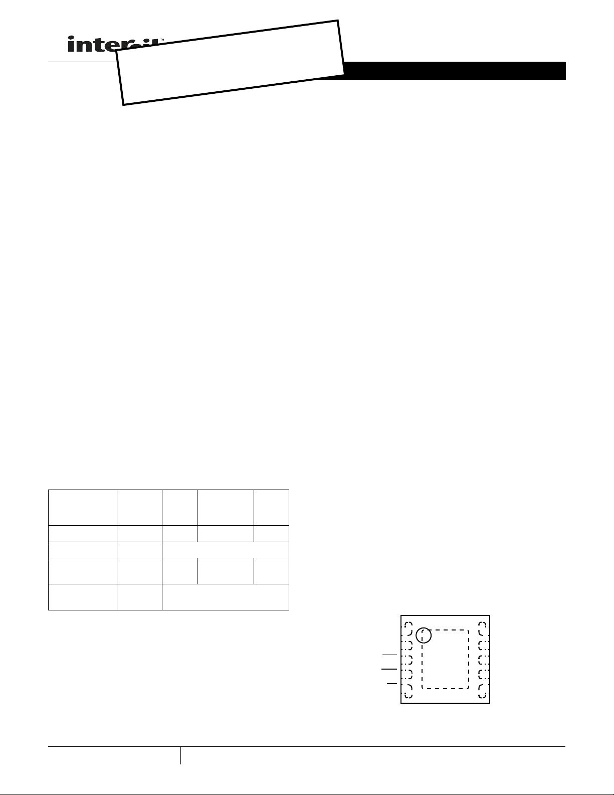
Block Diagram
USB
BAT
+
-
V
REF
VA
-
+
CA
I
R
ICDL
USBP
Reference
Current
Control
Temp
Monitor
ENA
CPPR
LBAT
CPPR
Control
USB
CRDL
BAT
PPR
CHG
EN
GND
CRDL
IUSB
ISL6293
2
FN9180.1
January 4, 2006
Page 3
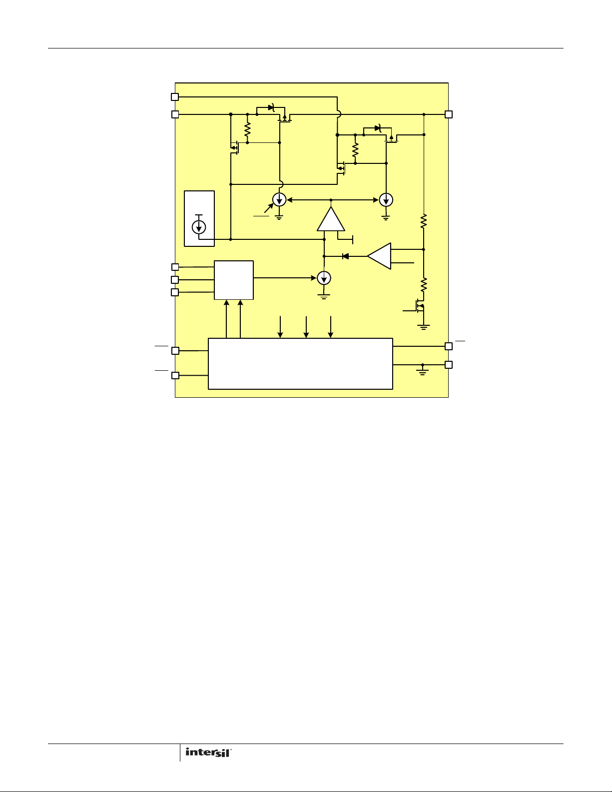
ISL6293-2
To Battery
CRDL
BAT
ICDL
USBP
To USB
Connector
C
1
R
3
C
3
USB
EN
CHG
C
2
To Cradle
Connector
R
ICDL
R
1
IUSB
R
IUSB
500mA
100mA
GND
PPR
R
2
D
1
D
2
Disable
Enable
A Simple Charger Accepting Power from Both a USB Port and a Desktop Cradle
A Simple Charger with Programmable Charge Current and Wide Input Voltage Range
COMPONENT SELECTION
R
ICDL
1.82k for 0.8A cradle charge current
R
IUSB
80k for 100mA/500mA USB charge current
R
2
, R
3
470
C
1
, C2, C31µF ceramic capacitor
R
1
1
D
1
, D
2
LEDs
COMPONENT SELECTION
R
ICDL
1.82k for 0.8A cradle charge current
C
1
, C
2
1µF ceramic capacitor
R
IUSB
is not required when the USB input of ISL6293-2 is left
floating in the design for a single input charger.
ISL6293-2
To Battery
USB
BAT
ICDL
GND
USBP
C
2
CRDL
CHG
PPR
C
1
To Cradle
Connector
R
ICDL
IUSB
Disable
Enable
EN
ISL6293
Typical Applications
3
FN9180.1
January 4, 2006
Page 4

ISL6293
Absolute Maximum Ratings Thermal Information
Supply Voltage (USB) . . . . . . . . . . . . . . . . . . . . . . . . . . . -0.3V to 7V
Supply Voltage (CRDL) . . . . . . . . . . . . . . . . . . . . . . . . . -0.3V to 28V
Signal Input Voltage (EN, USBP, ICDL, IUSB, BAT) . . . . -0.3V to 7V
Open-Drain Pull-Up Voltage (PPR, CHG) . . . . . . . . . . . . -0.3V to 7V
Recommended Operating Conditions
Ambient Temperature Range. . . . . . . . . . . . . . . . . . . . -40°C to 85°C
Supply Voltage (USB Pin) . . . . . . . . . . . . . . . . . . . . . . 4.3V to 5.5V
Supply Voltage (CRDL Pin) . . . . . . . . . . . . . . . . . . . . . . 4.3V to 24V
Typical Cradle Charge Current . . . . . . . . . . . . . . . . . . 300mA to 1A
Typical USB Charge Current . . . . . . . . . . . . . . . . 350mA to 450mA
CAUTION: Stresses above those listed in “Absolute Maximum Ratings” may cause permanent damage to the device. This is a stress only rating and operation of the
device at these or any other conditions above those indicated in the operational sections of this specification is not implied.
NOTES:
is measured in free air with the component mounted on a high effective thermal conductivity test board with “direct attach” features. See
1.
JA
Tech Brief TB379.
2. For
, the “case temp” location is the center of the exposed metal pad on the package underside.
JC
Thermal Resistance
(°C/W) JC (°C/W)
JA
3x3 DFN Package (Notes 1, 2) . . . . . . 46 4
Maximum Junction Temperature (Plastic Package) . . . . . . . . 150°C
Maximum Storage Temperature Range . . . . . . . . . . . -65°C to 150°C
Maximum Lead Temperature (Soldering 10s) . . . . . . . . . . . . . 300°C
Electrical Specifications Typical Values Are Tested at USB = CRDL = 5V and ambient temperature is at 25°C, Unless Otherwise Noted.
All Maximum and Minimum Values Are Guaranteed Under the Recommended Operating Conditions.
PARAMETER SYMBOL TEST CONDITIONS MIN TYP MAX UNITS
POWER-ON RESET
Rising USB/CRDL Threshold 3.4 3.7 4.0 V
Falling USB/CRDL Threshold 3.2 3.5 3.8 V
VIN-BAT OFFSET VOLTAGE
Rising Edge V
Falling Edge V
OS
V
= 4.0V, use CHG pin to indicate the
BAT
comparator output (Note 3)
OS
STANDBY CURRENT
BAT Pin Sink Current I
STANDBY
CRDL Pin Supply Current I
USB Pin Supply Current I
CRDL
USB
EN = HIGH or both inputs are floating 1.0 A
EN = HIGH 150 A
CRDL/USB Pin Supply Current EN = LOW or floating 0.55 mA
VOLTAGE REGULATION
Output Voltage (Note 4) V
CRDL PMOS On Resistance V
USB PMOS On Resistance V
Charge current = 20mA 4.158 4.2 4.242 V
CH
BAT
BAT
= 3.8V, I
= 3.8V, I
CHARGER
CHARGER
= 0.5A 700 m
= 0.35A 700 m
CHARGE CURRENT (Note 5)
ICDL Pin Output Voltage V
IUSB Pin Output Voltage V
CRDL Input Constant Charge Current I
CHARGERICDL
ICDLVBAT
IUSB
= 3.8V 1.17 1.20 1.23 V
0.776 0.8 0.824 V
= 1.82k, V
BAT
= 3.8V
720 800 880 mA
Valid for -10°C to 85°C
CRDL Input Trickle Charge Current I
TRICKLERICDL
Given as a percentage of the CRDL I
= 1.82k, V
BAT
= 2.4V
CHARGE
9.2 13.2 17.2 %
Valid for -10°C to 85°C
USB Input Constant Charge Current I
USB Input Trickle Charge Current (Note 4) I
CHARGE
TRICKLE
USBP = HIGH, R
USBP = HIGH, R
IUSB
IUSB
= 80k, V
= 80k, V
= 3.8V 380 440 500 mA
BAT
BAT
= 2.4V
8.0 10.0 12.0 %
Given as a percentage of the USB HIGH
I
CHARGE
175 mV
110 mV
150 250 A
4
FN9180.1
January 4, 2006
Page 5

ISL6293
Electrical Specifications Typical Values Are Tested at USB = CRDL = 5V and ambient temperature is at 25°C, Unless Otherwise Noted.
All Maximum and Minimum Values Are Guaranteed Under the Recommended Operating Conditions. (Continued)
PARAMETER SYMBOL TEST CONDITIONS MIN TYP MAX UNITS
USB Input Constant Charge Current I
USB Input Trickle Charge Current I
END-OF-CHARGE CURRENT THRESHOLD
Powered From USB Pin I
Powered From USB Pin I
Powered From CRDL Pin I
PRECONDITIONING CHARGE THRESHOLD
Preconditioning Charge Threshold Voltage V
INTERNAL TEMPERATURE MONITORING
Current Foldback Threshold (Note 5) T
LOGIC INPUT AND OUTPUT
USBP Pin Logic Input High 2.0 V
USBP Pin Logic Input Low 0.4 V
USBP Pin Internal Pull Down Resistance 1000 k
EN Pin Logic Input High 1.2 V
EN Pin Logic Input Low 0.4 V
EN Pin Internal Pull Down Resistance 1000 k
CHG/PPR Sink Current Pin Voltage = 0.8V 15 mA
NOTES:
3. The 4.0V V
than the POR threshold, no output pin can be used for indication.
4. The maximum and minimum limits are guaranteed over -40°C to 70°C ambient temperature range.
5. The charge current may be reduced by the thermal foldback function, depending on the heatsinking condition of the test setup.
6. The threshold value at which the charger output is reduced to near zero. Guaranteed by characterization or correlation to other test.
is selected so that the CHG output can be used as the indication for the offset comparator output indication. If the V
BAT
CHARGE
TRICKLE
EOC
EOC
EOC
FOLD
USBP = LOW, R
USBP = LOW, R
Given as a percentage of the USB LOW
I
CHARGE
USBP = HIGH, R
Given as a percentage of the USB HIGH
I
CHARGE
USBP = LOW, R
Given as a percentage of the USB LOW
I
CHARGE
R
= 1.82k,
ICDL
Given as a percentage of the CRDL I
MIN
IUSB
IUSB
IUSB
IUSB
= 80k, V
= 80k, V
= 80k
= 80k
= 3.8V 68 84 100 mA
BAT
BAT
= 2.4V
CHARGE
45.0 50.0 55.0 %
8.0 10.5 13.0 %
17.0 21.0 25.0 %
5.5 8.5 11.0 %
2.5 2.6 2.7 V
85 100 115 °C
BAT
is lower
Functional Pin Description
CRDL (Pin 1)
Cradle input. This pin is usually connected to a cradle power
input. The maximum input voltage is 28V. The charge
current from this pin is programmable with the ICDL pin up to
1A. When this pin is connected to a power source, no charge
current is drawn from the USB pin. A 1µF or larger value
ceramic capacitor is recommended for decoupling.
USB (Pin 2)
USB input. This pin is usually connected to a USB port
power connector. Other sources that are lower than 5.5V are
also acceptable. The charge current from the USB pin is
selectable between 100mA and 500mA maximum with the
5
USBP pin when the R
= 80k. A 1µF or larger value
IUSB
ceramic capacitor is recommended for decoupling. It is also
recommended to have a 1 resistor in series with the
decoupling capacitor to prevent an over-shoot voltage when
a USB hot plug event occurs.
PPR (Pin 3)
Power presence indication. This is an open-drain output pin
that outputs a logic LOW when either the USB input voltage
or the CRDL input voltage is above its POR level, regardless
if the charger is enabled or disabled. This pin provides a
wake-up signal to a microprocessor when either the cradle
or the USB power is connected.
FN9180.1
January 4, 2006
Page 6

I
USB
45000
V
REF
R
IUSB
------------------
45000
0.8V
R
IUSB
------------------
A==
I
CDL
1.20V
R
ICDL
-----------------
ratio= A
FIGURE 1. THE RATIO USED IN THE CHARGE CURRENT
CALCULATION vs. R
ICDL
1280
1250
1220
1190
1160
1130
1100
1070
12345
RATIO
R
ICDL
(k)
V
ICDL
1.20V
I
CDL
----------------
I
CHG
R
ICDLICHG
ratio
------------------------------------
==
ISL6293
CHG (Pin 4)
Charge indication pin. When the charge current from the
cradle input during the constant current mode falls to below
8% of the programmed reference current by the ICDL pin or
the charge current from the USB input is below 10% of the
programmed charge current, the open-drain MOSFET is
turned off. The pin will be pulled to logic HIGH by an external
resistor to indicate the End Of Charge.
EN (Pin 5)
Enable logic input. Connect to LOW or leave floating to
enable the charger.
IUSB (Pin 6)
The IUSB pin programs the USB charge current. This pin is
regulated to 0.8V. The current flowing out of this pin is
mirrored to the USB charge current control reference. When
the USBP pin is connected to logic HIGH, the typical USB
charge current can be found as:
The R
has a programming range of 80k to 103k,
IUSB
thus the USB current has a nominal value ranging from
350mA to 450mA.
When the USBP pin is driven to logic LOW, the charge
current is approximately 1/5 of the above value.
USBP (Pin 7)
USB port selection logic input. When this pin is left floating or
driven to logic LOW, the USB port is regarded as a
low-power port, in such case the charge current is 100mA
maximum. When this pin is driven to logic HIGH, the USB
port is considered a high-power port, and the charge current
is 500mA maximum. The ratio of the charge current when
this pin is HIGH or LOW is fixed at approximately 5:1.
GND (Pin 8)
System ground.
ICDL (Pin 9)
The ICDL pin has two functions. The first function is to
program the cradle charge current during the constantcurrent phase. The voltage of this pin is 1.20V during the
constant-current phase of the cradle input charger. The
constant-current is programmed by the following equation:
where R
Typical Application). The ratio is given by the following table
and curve.
is the resistor connected to the ICDL pin (see
ICDL
6
TABLE 1. RATIO vs. R
R
(k) 1.5 2.2 3.0 3.9 4.6
ICDL
Ratio 1291 1216 1155 1122 1088
ICDL
It is recommended that the charge current be programmed
in the range of 300mA to 1A.
The second function of the ICDL pin is to monitor the actual
charge current. The voltage of this pin, V
to the actual charge current, I
, in either the USB or the
CHG
, is proportional
ICDL
cradle charger. When the cradle charger or the USB charger
is working with USBP connected to logic HIGH, the ICDL pin
voltage is given by the following equation:
where the ratio has the same value given in Table 1.
The cradle charge current should be programmed equal or
higher than the USB current; otherwise, the ICDL pin voltage
will be higher than 1.20V during the constant current phase
when the USB charger is working. The charger still works
properly but the accuracy of the current monitoring voltage
degrades and saturates at approximately 2.1V.
When the USB charger is working with the USBP pin
connected to logic LOW, the ICDL pin voltage is
approximately five times of the above equation.
BAT (Pin 10)
Charger output pin. Connect this pin to the battery pack or
the battery cell. A 1µF or larger value ceramic capacitor is
recommended for decoupling. The charger relies on the
battery for stability so a battery should always be connected
to the BAT pin.
FN9180.1
January 4, 2006
Page 7

I
TRICKLE
1.20V
R
ICDL
-----------------
100= A
ISL6293
Description
The ISL6293 is designed for a single-cell Li-ion or Li-polymer
battery charging circuit that accepts both a USB port and a
desktop cradle as its power source. The charge current from
each power source is independently programmable but only
one of the two sources charges the battery. The following
describes the operation of the charger.
Input Auto Selection
When both input sources are present, the charger selects
only one power source to charge the battery. When the
CRDL input is higher than both the POR threshold and the
battery voltage, CRDL is selected as the power source.
Otherwise the USB input is selected. If the CRDL input
voltage is below the battery voltage but the USB input
voltage is higher than the battery voltage, then the USB input
is used to charge the battery. The control circuit always
breaks both internal power devices before switching in one
power source to avoid any simultaneous conduction of both
power MOSFETs.
When the BAT pin voltage is below 1.7V, the charger selects
the CRDL input as the power source. Hence, if the USB
input is powered, the charger will not charge the battery.
USB Charge Current
When the USB port is selected as the power source, the
charge current is programmed by the logic input USBP pin.
With the R
to logic LOW, the charge current is set to 90mA. When the
USBP is driven to logic HIGH, the charge current is set to
450mA. The USBP is equivalent to a logic LOW when left
floating. Typically the P-channel MOSFET for the USB input
has an r
500mA charge current, the typical head room is 350mV. If
the input voltage drops to a level that the voltage different
between the USB pin and the BAT pin is less than 350mV,
the r
DS(ON)
and the charge current drops out the constant current
regulation.
selected at 80k, when the USBP is driven
IUSB
of 700m at room temperature, thus with a
DS(ON)
becomes a limiting factor of the charge current
Floating Charge Voltage
The floating voltage during the constant voltage phase is
4.2V. The floating voltage has an 1% accuracy over the
ambient temperature range of -40°C to 70°C.
Trickle Charge Current
When the battery voltage is below the minimum battery
voltage V
given in the electrical specification, the charger
MIN
operates in a trickle/preconditioning mode. If power comes
from the cradle, the trickle mode current is
The trickle current is 45mA if the power comes from the USB
port with R
IUSB
= 80k.
End-of-Charge Indication
The CHG pin outputs a logic HIGH by turning off the internal
open-drain MOSFET when the charge current falls below
8% of the constant current mode current for the cradle input
or 10% for the USB input when R
is 80k. The charger,
IUSB
however, does not turn off as long as an input power source
is attached.
Power Presence Indication
When either the USB or the cradle input voltage is above the
POR level, the PPR pin outputs a logic LOW signal to
indicate the presence of input power.
Cradle Charge Current
The cradle charge current is programmed with the external
resistor connected between the ICDL pin and the GND pin.
The current can be calculated with the equation given in the
ICDL pin description. The typical r
channel MOSFET for the CRDL input is 700m at room
temperature, thus when the head room between the input
and output voltages is small, the actual charge current,
similar to the USB case, could be limited by the r
the other hand, if the head room between the input and
output voltages is large, the charge current maybe limited by
the thermal foldback threshold due to the increased power
dissipation.
7
DS(ON)
value of the P-
DS(ON).
On
FN9180.1
January 4, 2006
Page 8

Dual Flat No-Lead Plastic Package (DFN)
D
E
A
B
0.10 MC
e
0.415
C
SECTION "C-C"
NX (b)
(A1)
2X
C
0.15
0.152XB
NX L
REF.
(Nd-1)Xe
5
A
C
(DATUM B)
D2
D2/2
E2
E2/2
TOP VIEW
7
BOTTOM VIEW
5
6
INDEX
AREA
8
AB
NX
k
6
INDEX
AREA
(DATUM A)
12
N-1N
NX b
8
NX b
NX L
0.200
C
A
SEATING
PLANE
0.08
C
A3
SIDE VIEW
0.10 C
FOR ODD TERMINAL/SIDE
C
L
e
TERMINAL TIP
L
CC
ISL6293
L10.3x3
10 LEAD DUAL FLAT NO-LEAD PLASTIC PACKAGE
MILLIMETERS
SYMBOL
A 0.80 0.90 1.00 -
A1 - - 0.05 -
A3 0.20 REF -
b 0.18 0.23 0.28 5,8
D 3.00 BSC -
D2 1.95 2.00 2.05 7,8
E 3.00 BSC -
E2 1.55 1.60 1.65 7,8
e 0.50 BSC -
k0.25 - - -
L 0.30 0.35 0.40 8
N102
Nd 5 3
NOTES:
1. Dimensioning and tolerancing conform to ASME Y14.5-1994.
2. N is the number of terminals.
3. Nd refers to the number of terminals on D.
4. All dimensions are in millimeters. Angles are in degrees.
5. Dimension b applies to the metallized terminal and is measured
between 0.15mm and 0.30mm from the terminal tip.
6. The configuration of the pin #1 identifier is optional, but must be
located within the zone indicated. The pin #1 identifier may be
either a mold or mark feature.
7. Dimensions D2 and E2 are for the exposed pads which provide
improved electrical and thermal performance.
8. Nominal dimensions are provided to assist with PCB Land
Pattern Design efforts, see Intersil Technical Brief TB389.
NOTESMIN NOMINAL MAX
Rev. 3 6/04
Intersil products are sold by description only. Intersil Corporation reserves the right to make changes in circuit design, software and/or specifications at any time without
notice. Accordingly, the reader is cautioned to verify that data sheets are current before placing orders. Information furnished by Intersil is believed to be accurate and
reliable. However, no responsibility is assumed by Intersil or its subsidiaries for its use; nor for any infringements of patents or other rights of third parties which may result
from its use. No license is granted by implicat ion or oth erwise u nde r any p a tent or p at ent r ights of Intersil or its subsidiaries.
All Intersil U.S. products are manufactured, assembled and tested utilizing ISO9001 quality systems.
Intersil Corporation’s quality certifications can be viewed at www.intersil.com/design/quality
For information regarding Intersil Corporation and its products, see www.intersil.com
8
FN9180.1
January 4, 2006
Page 9

 Loading...