

Page 1

®
N
R
O
F
D
E
D
N
E
T
O
N
O
C
E
R
M
M
D
N
E
E
R
D
E
6
L
S
I
M
M
O
C
E
R
E
C
A
L
P
A
5
6
2
E
D
W
E
T
N
E
M
Data Sheet May 13, 2009
S
N
G
I
S
T
R
A
P
ISL6265
FN6599.1
Multi-Output Controller with Integrated
MOSFET Drivers for AMD SVI Capable
Mobile CPUs
The ISL6265 is a multi-output controller with embedded gate
drivers. A single-phase controller powers the Northbridge
(VDDNB) portion of the CPU. The two remaining controller
channels can be configured for two-phase or individual
single-phase outputs. For uniplane CPU applications, the
ISL6265 is configured as a two-phase buck converter. This
allows the controller to interleave channels to effectively
double the output voltage ripple frequency and thereby
reduce output voltage ripple amplitude with fewer
components, lower component cost, reduced power
dissipation, and smaller area. For dual-plane processors, the
ISL6265 can be configured as independent single-phase
controllers powering VDD0 and VDD1.
The heart of the ISL6265 is the patented R
Intersil’s Robust Ripple Regulator modulator. Compared with
the traditional buck regulator, the R
3
faster transient response. This is due to the R
commanding variable switching frequency during a load
transient.
The Serial VID Interface (SVI) allows dynamic adjustment of
the Core and Northbridge output voltages independently and
in combination from 0.500V to 1.55V. Core and Northbridge
output voltages achieve a 0.5% system accuracy
over-temperature.
3
Technology™,
Technology™ has a
3
modulator
Features
• Core Configuration Flexibility
- Dual Plane, Single-Phase Controllers
- Uniplane, Two-Phase Controller
• Precision Voltage Regulators
- 0.5% System Accuracy Over-temperature
• Voltage Positioning with Adjustable Load Line and Offset
• Internal Gate Drivers with 2A Driving Capability
• Differential Remote CPU Die Voltage Sensing
• Core Differential Current Sensing: DCR or Resistor
• Northbridge Lossless r
• Serial VID Interface
- Two Wire Clock and Data Bus
- Supports High-Speed I
- 0.500V to 1.55V in 12.5mV Steps
- Supports PSI_L Power-Saving Mode
• Core Outputs Feature Phase Shedding with PSI_L
• Adjustable Output-Voltage Offset
• Digital Soft-Start of all Outputs
• User Programmable Switching Frequency
• Static and Dynamic Current Sharing (Uniplane Core)
• Overvoltage, Undervoltage, and Overcurrent Protection
• Pb-Free (RoHS Compliant)
Current Sensing
DS(ON)
2
C
A unity-gain differential amplifier is provided for remote CPU
die sensing. This allows the voltage on the CPU die to be
accurately regulated per AMD mobile CPU specifications.
Core output current sensing is realized using lossless
inductor DCR sensing. All outputs feature overcurrent,
overvoltage and undervoltage protection.
Ordering Information
PART NUMBER
(Note)
ISL6265HRTZ ISL6265 HRTZ -10 to +100 48 Ld 6x6 TQFN L48 .6x6
ISL6265HRTZ-T* ISL6265 HRTZ -10 to +100 48 Ld 6x6 TQFN
* Please refer to TB347 for details on reel specifications.
NOTE: These Intersil Pb-free plastic packaged products employ special
Pb-free material sets; molding compounds/die attach materials and 100%
matte tin plate PLUS ANNEAL - e3 termination finish, which is RoHS
compliant and compatible with both SnPb and Pb-free soldering
operations. Intersil Pb-free products are MSL classified at Pb-free peak
reflow temperatures that meet or exceed the Pb-free requirements of
IPC/JEDEC J STD-020.
PART
MARKING TEMP (°C)
1
PACKAGE
(Pb-Free)
Tape and Reel
PKG.
DWG. #
L48.6x6
CAUTION: These devices are sensitive to electrostatic discharge; follow proper IC Handling Procedures.
1-888-INTERSIL or 1-888-468-3774
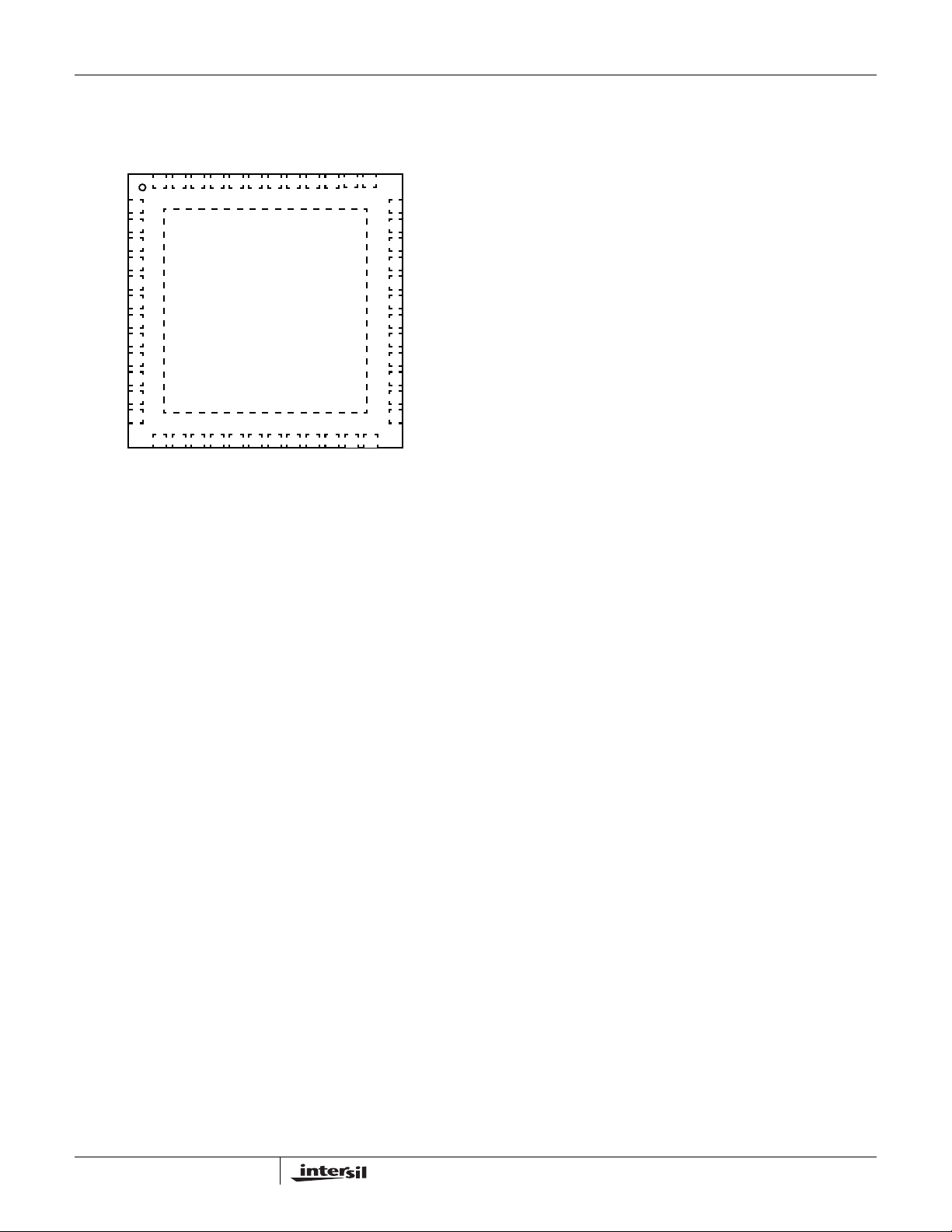
Pinout
OFS/VFIXEN
PGOOD
PWROK
SVD
SVC
ENABLE
RBIAS
OCSET
VDIFF_0
FB_0
COMP_0
VW0
ISL6265 (48 LD 6X6 TQFN)
TOP VIEW
PHASE_NB
VCC
FB_NB
COMP_NB
VSEN_NB
VIN
48
47 46 45 44 43 42 41 40 39
1
2
3
4
5
6
7
8
9
10
11
12
13 14 15 16 17 18 19 20 21 22
ISP0
ISN0
RTN0
VSEN0
| Intersil (and design) is a registered trademark of Intersil Americas Inc.
Copyright Intersil Americas Inc. 2008, 2009. All Rights Reserved
All other trademarks mentioned are the property of their respective owners.
RTN_NB
FSET_NB
RTN1
49
GND
VSEN1
VDIFF_1
OCSET_NB
FB_1
PGND_NB
COMP_1
LGATE_NB
VW1
38 37
23 24
ISP_1
UGATE_NB
BOOT_NB
36
BOOT_0
35
UGATE_0
34
PHASE_0
33
PGND_0
32
LGATE_0
31
PVCC
30
LGATE_1
29
PGND_1
28
PHASE_1
27
UGATE_1
26
BOOT_1
25
ISN_1
Page 2
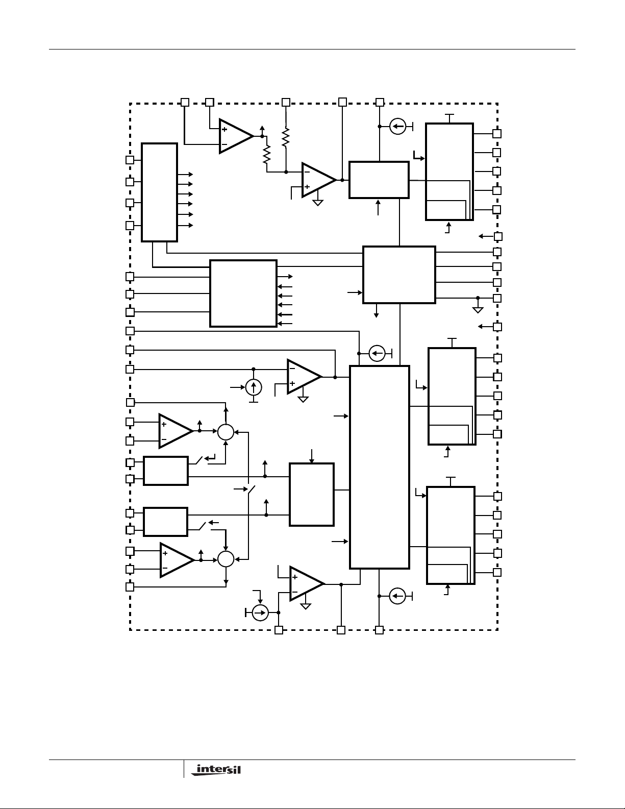
Function Block Diagram
ISL6265
SVC
SVD
PWROK
OFS/FIXEN
OCSET_NB
OCSET
RBIAS
VW0
COMP0
FB0
VDIFF0
VSEN0
RTN0
ISP0
ISN0
ISP1
ISN1
VSEN1
RTN1
VDIFF1
RTN_NB
SVI
INTERFACE
AND DAC
1
CURRENT
SENSE
CURRENT
SENSE
1
VSEN_NB
NO DROOP
PSI_L
I_OFS
VREF_NB
VREF0
VREF1
I_OFS
V0
NO
DROOP
MODE
V1
VNB
1
1.5kΩ
FAULT
PROTECTION
∑
ISEN0
ISEN1
NO
DROOP
∑
I_OFS
FB_NB
1.5kW
VREF_NB
VREF0
VREF1
3.0kΩ
E/A
FLT
VNB
V0
V1
ISEN0
ISEN1
E/A
VIN
MODE
CURRENT
BALANCE
MODE
E/A
COMP_NB
RTN1
FSET_NB
I
FSET_NB
MODULATOR
NB
VIN
POWER-ON
RESET AND
SOFT-START
LOGIC
MODE
I
VW0
MODULATOR
CORE
I
VW1
FLT
PROTECTION
PSI_L
FLT
PSI_L
FLT
PSI_L
PVCC
MOSFET
DRIVER
SHOOT-THRU
DE MODE
PVCC
MOSFET
DRIVER
SHOOT-THRU
PROTECTION
DE MODE
PVCC
MOSFET
DRIVER
SHOOT-THRU
PROTECTION
DE MODE
BOOT_NB
UGATE_NB
PHASE_NB
LGATE_NB
PGND_NB
PVCC
VCC
ENABLE
PGOOD
GND
VIN
BOOT0
UGATE0
PHASE0
LGATE0
PGND0
BOOT1
UGATE1
PHASE1
LGATE1
PGND1
FB1
COMP1
VW1
FIGURE 1. SIMPLIFIED FUNCTION BLOCK DIAGRAM OF ISL6265
2
FN6599.1
May 13, 2009
Page 3
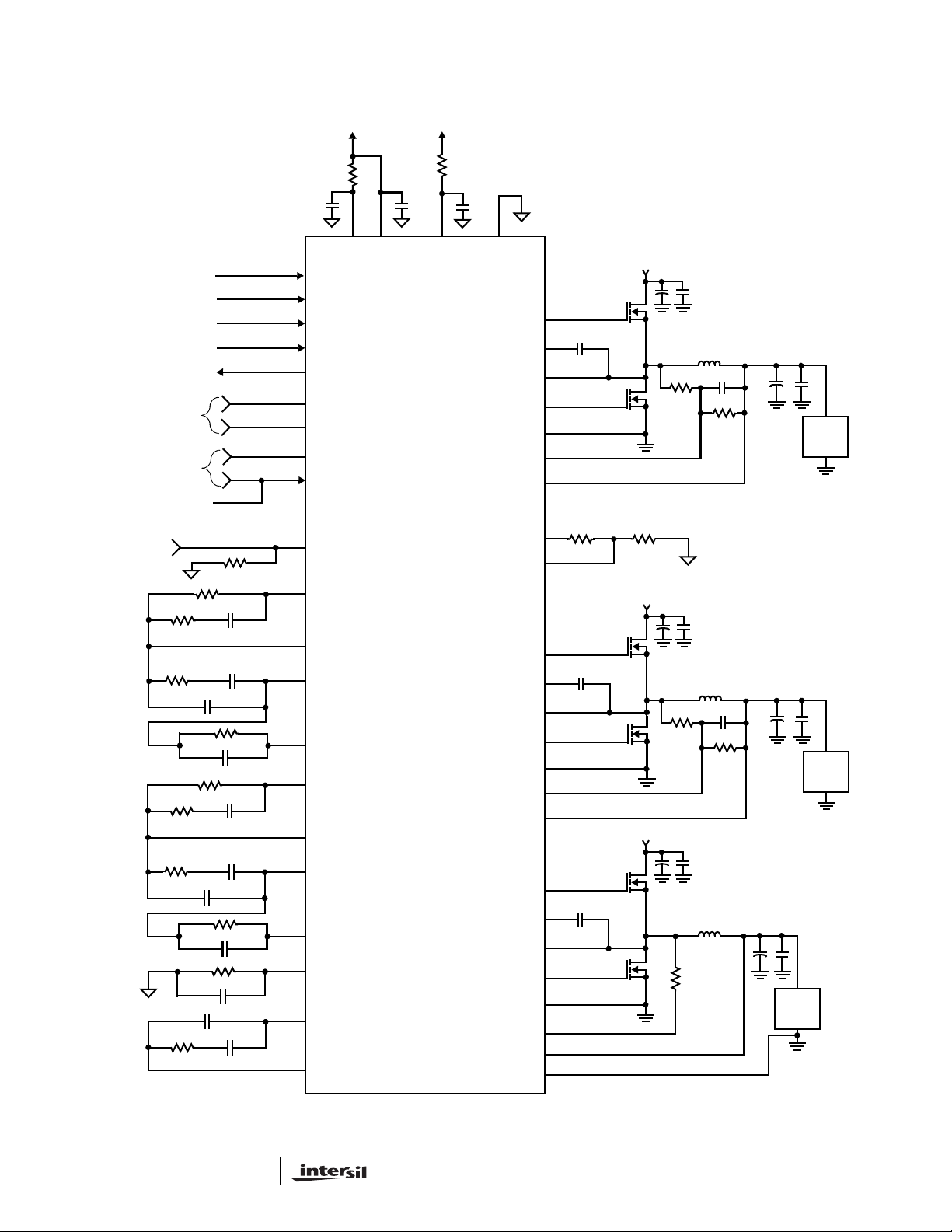
ISL6265
Simplified Application Circuit for Dual Plane and Northbridge Support
SVI DATA
SVI CLOCK
ENABLE
PWROK
VDDPWRGD
REMOTE
SENSE
REMOTE
SENSE
VDD_PLANE_STRAP
+5V
VCC
SVD
SVC
EN
PWROK
PGOOD
VSEN0
RTN0
VSEN1
RTN1
OFS/VFIXEN
PVCC
VIN
VIN
GND
UGATE0
BOOT0
PHASE0
LGATE0
PGND0
OCSET
ISP0
ISN0
RBIAS
+VIN
C
IN
L
OUT
VDD0
CORE
LOAD
VDIFF0
FB0
COMP0
VW0
VDIFF1
FB1
COMP1
VW1
FSET_NB
COMP_NB
FB_NB
ISL6265
UGATE1
BOOT1
PHASE1
LGATE1
PGND1
ISP1
ISN1
UGATE_NB
BOOT_NB
PHASE_NB
LGATE_NB
PGND_NB
OCSET_NB
VSEN_NB
RTN_NB
+VIN
+VIN
C
IN
L
OUT
C
IN
L
OUT
VDD1
VDDNB
NB
LOAD
CORE
LOAD
FIGURE 2. ISL6265 BASED DUAL-PLANE AND NORTHBRIDGE CONVERTERS WITH INDUCTOR DCR CURRENT SENSING
3
May 13, 2009
FN6599.1
Page 4
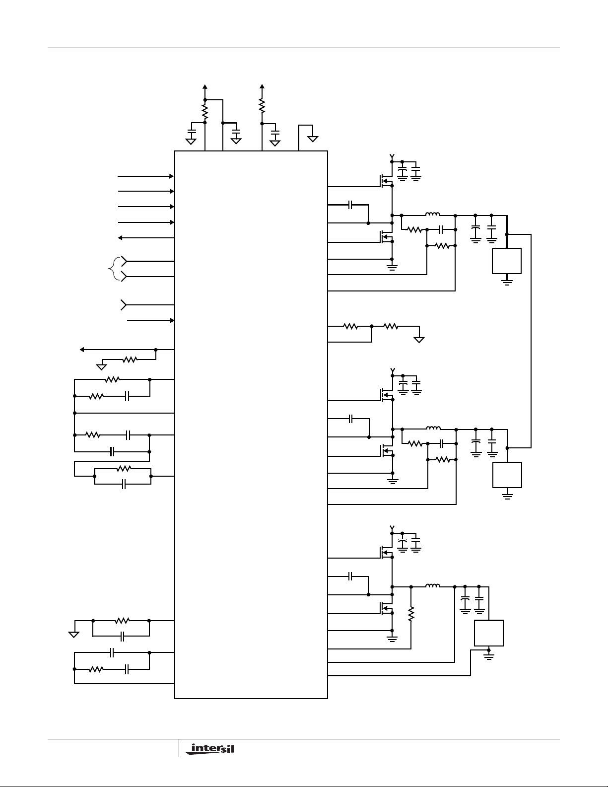
ISL6265
Simplified Application Circuit for Uniplane Core and Northbridge Support
+5V
SVI DATA
SVI CLOCK
ENABLE
PWROK
VDDPWRGD
REMOTE
SENSE
REMOTE
SENSE
VDD_PLANE_STRAP
VCC
SVD
SVC
EN
PWROK
PGOOD
VSEN0
RTN0
VSEN1
RTN1
OFS/VFIXEN
VDIFF0
FB0
COMP0
PVCC
ISL6265
VIN
GND
UGATE0
BOOT0
PHASE0
LGATE0
PGND0
RBIAS
OCSET
UGATE1
BOOT1
PHASE1
ISP0
ISN0
+VIN
+VIN
C
IN
L
OUT
CORE
LOAD
VDD0
C
IN
L
OUT
LGATE1
VDDNB
NB
LOAD
CORE
LOAD
OPEN
OPEN
OPEN
OPEN
VW0
VDIFF1
FB1
COMP1
VW1
FSET_NB
COMP_NB
FB_NB
PGND1
ISP1
ISN1
UGATE_NB
BOOT_NB
PHASE_NB
LGATE_NB
PGND_NB
OCSET_NB
VSEN_NB
RTN_NB
+VIN
C
IN
L
OUT
FIGURE 3. ISL6265 BASED UNIPLANE AND NORTHBRIDGE CONVERTERS WITH INDUCTOR DCR CURRENT SENSING
4
FN6599.1
May 13, 2009
Page 5
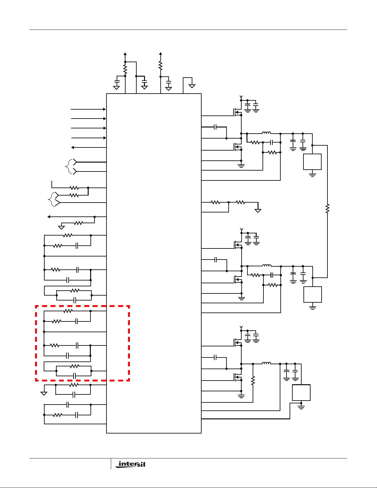
ISL6265
Simplified Application Circuit for Dual Layout
+5V
SVI DATA
SVI CLOCK
ENABLE
PWROK
VDDPWRGD
REMOTE
SENSE
VDD_PLANE_STRAP
REMOTE
SENSE
DNP DUAL PLANE
DNP UNIPLANE
VCC
SVD
SVC
EN
PWROK
PGOOD
VSEN0
RTN0
RTN1
VSEN1
OFS/VFIXEN
VDIFF0
FB0
COMP0
PVCC
ISL6265
VIN
GND
UGATE0
BOOT0
PHASE0
LGATE0
PGND0
RBIAS
OCSET
UGATE1
BOOT1
PHASE1
ISP0
ISN0
+VIN
+VIN
C
IN
L
OUT
VDD0
CORE
LOAD
UNIPLANE
VDD0
C
IN
L
OUT
DNP
DUAL
PLANE
LGATE1
VDDNB
NB
LOAD
CORE
LOAD
POPULATION OPTIONAL IN UNIPLANE
VW0
VDIFF1
FB1
COMP1
VW1
FSET_NB
COMP_NB
FB_NB
PGND1
ISP1
ISN1
UGATE_NB
BOOT_NB
PHASE_NB
LGATE_NB
PGND_NB
OCSET_NB
VSEN_NB
RTN_NB
+VIN
C
IN
L
OUT
FIGURE 4. ISL6265 BASED UNIPLANE OR DUAL PLANE CORE CONVERTER WITH IN DUCTOR DCR CURRENT SENSING
VDD1
5
FN6599.1
May 13, 2009
Page 6
ISL6265
Absolute Maximum Ratings Thermal Information
Supply Voltage, VCC, PVCC . . . . . . . . . . . . . . . . . . . . . . .-0.3 - +7V
Battery Voltage, VIN. . . . . . . . . . . . . . . . . . . . . . . . . . . . . . . . . +28V
Boot Voltage (BOOT). . . . . . . . . . . . . . . . . . . . . . . . . -0.3V to +33V
Boot to Phase Voltage (BOOT-PHASE). . . . . . . . -0.3V to +7V(DC)
. . . . . . . . . . . . . . . . . . . . . . . . . . . . . . . . . . . -0.3V to +9V (<10ns)
Phase Voltage (PHASE) . . . . . . . . . -7V (<20ns Pulse Width, 10µJ)
UGATE Voltage (UGATE) . . . . . . . . . PHASE -0.3V (DC) to BOOT
LGATE Voltage (LGATE) . . . . . . . . . . . . . -0.3V (DC) to VCC + 0.3V
ALL Other Pins. . . . . . . . . . . . . . . . . . . . . . . . -0.3V to (VCC + 0.3V)
Open Drain Outputs, PGOOD . . . . . . . . . . . . . . . . . . . . . -0.3 - +7V
CAUTION: Do not operate at or near the maximum ratings listed for extended periods of time. Exposure to such conditions may adversely impact product reliability and
result in failures not covered by warranty.
NOTES:
is measured in free air with the component mounted on a high effective thermal conductivity test board with “direct attach” features. See T ech
1. θ
JA
Brief TB379.
2. For θ
, the “case temp” location is the center of the exposed metal pad on the package underside.
JC
Thermal Resistance (Typical, Notes 1, 2) θ
(°C/W) θJC (°C/W)
JA
TQFN Package . . . . . . . . . . . . . . . . . . 30 1.5
Maximum Junction Temperature . . . . . . . . . . . . . . . . . . . . . . +150°C
Maximum Storage Temperature Range. . . . . . . . . .-65°C to +150°C
Pb-free reflow profile . . . . . . . . . . . . . . . . . . . . . . . . . .see link below
http://www.intersil.com/pbfree/Pb-FreeReflow.asp
Recommended Operating Conditions
Supply Voltage, VCC, PVCC. . . . . . . . . . . . . . . . . . . . . . . .+5V ±5%
Battery Voltage, VIN . . . . . . . . . . . . . . . . . . . . . . . . . . . . +6V to 24V
Ambient Temperature . . . . . . . . . . . . . . . . . . . . . . .-10°C to +100°C
Junction Temperature . . . . . . . . . . . . . . . . . . . . . . .-10°C to +125°C
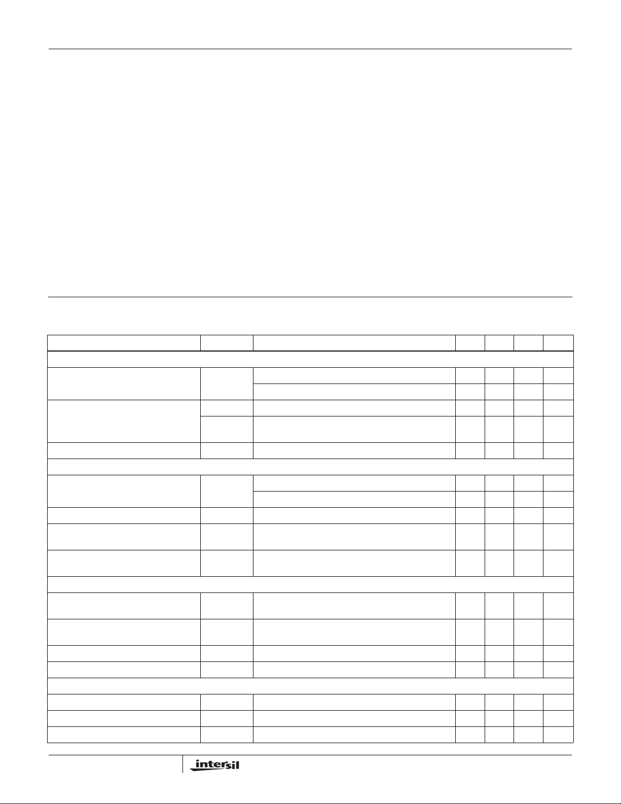
Electrical Specifications VCC = PVCC = 5V , V
= 12V, TA = -10°C to +100°C; Parameters with MIN and/or MAX limits are 100% tested
IN
at +25°C, unless otherwise specified. T emperature limits est ablished by characterization and are not production
tested.
PARAMETER SYMBOL TEST CONDITIONS MIN TYP MAX UNITS
INPUT POWER SUPPLY
+5V Supply Current I
VCC
EN = 3.3V - 7.8 10 mA
EN = 0V - - 1 µA
POR (Power-On Reset) Threshold VCC POR
VCC POR
Battery Supply Current (VIN) I
VIN
Rising - 4.35 4.5 V
rVCC
Falling 3.9 4.1 - V
fVCC
EN = 0V, VIN = 24V - - 1 µA
SYSTEM AND REFERENCES
System Accuracy
(V
core0, Vcore1, Vcore_NB
)
RBIAS Voltage R
Maximum Output Voltage (Note 3) V
Minimum Output Voltage (Note 3) V
%Error
(V
CORE
RBIAS
COREx
(max)
COREx
(min)
No load, closed loop, active mode VID = 0.75V to 1.55V -0.5 - 0.5 %
)
VID = 0.50V to 0.7375V -5 - +5 mV
R
= 117kΩ 1.15 1.17 1.19 V
RBIAS
SVID = [000_0000b] - 1.55 - V
SVID = [101_0100b] - 0.500 - V
CHANNEL FREQUENCY
Nominal CORE Switching Frequency f
Nominal NB Switching Frequency f
SW_core0
SW_core_NBRFSET_NB
VIN = 15.5V, V
force V
comp_0
= 22.1kΩ, C
V
= 0.51V
sen_nb
= 1.55V, V
DAC
=2V, R
= 1.60V,
FB0
= 6.81kΩ, 2-Phase Operation
VW
FSET_NB
= 1nF, V
DAC
= 0.5V,
285 300 315 kHz
285 300 315 kHz
Core Frequency Adjustment Range 200 - 500 kHz
NB Frequency Adjustment Range 200 - 500 kHz
AMPLIFIERS (Note 3)
Error Amp DC Gain A
V0
Error Amp Gain-Bandwidth Product GBW C
Error Amp Slew Rate SR C
= 20pF - 18 - MHz
L
= 20pF - 5.0 - V/µs
L
-90-dB
6
FN6599.1
May 13, 2009
Page 7
ISL6265
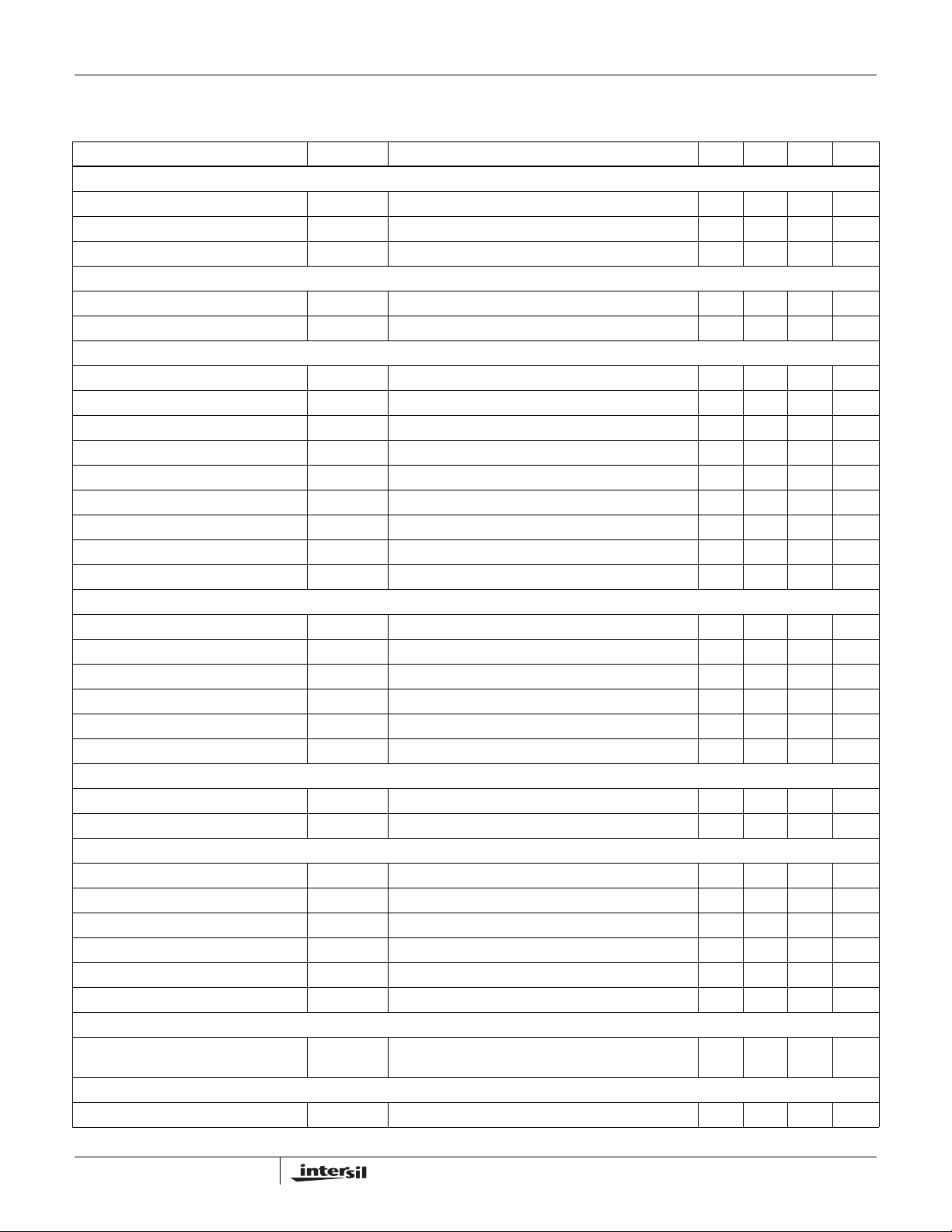
Electrical Specifications VCC = PVCC = 5V , V
at +25°C, unless otherwise specified. T emperature limits est ablished by characterization and are not production
= 12V, TA = -10°C to +100°C; Parameters with MIN and/or MAX limits are 100% tested
IN
tested. (Continued)
PARAMETER SYMBOL TEST CONDITIONS MIN TYP MAX UNITS
CORE CURRENT SENSE (Note 3)
Current Imbalance Threshold Di -4-mV
Input Bias Current -20-nA
RTN1 Threshold -0.8- V
SOFT START/VID-ON-THE-FLY
Soft-Start Voltage Transition V
SS
1.25 1.875 2.50 mV/µs
VID on the Fly Transition 5 7.5 10 mV/µs
GATE DRIVER DRIVING CAPABILITY [CORE AND NB]
UGATE Source Resistance (Note 4) R
UGATE Source Current (Note 4) I
UGATE Sink Resistance (Note 4) R
UGATE Sink Current (Note 4) I
LGATE Source Resistance (Note 4) R
LGATE Source Current (Note 4) I
LGATE Sink Resistance (Note 4) R
LGATE Sink Current (Note 4) I
UGATE to PHASE Resistance (Note 3) R
SRC(UGATE)
SRC(UGATE)VUGATE_PHASE
SNK(UGATE)
SNK(UGATE)VUGATE_PHASE
SRC(LGATE)
SRC(LGATE)VLGATE
SNK(LGATE)
SNK(LGATE)VLGATE
p(UGATE)
500mA Source Current - 1 1.5 Ω
= 2.5V - 2 - A
500mA Sink Current - 1 1.5 Ω
= 2.5V - 2 - A
500mA Source Current - 1 1.5 Ω
= 2.5V - 2 - A
500mA Sink Current - 0.5 0.9 Ω
= 2.5V - 4 - A
-1-kΩ
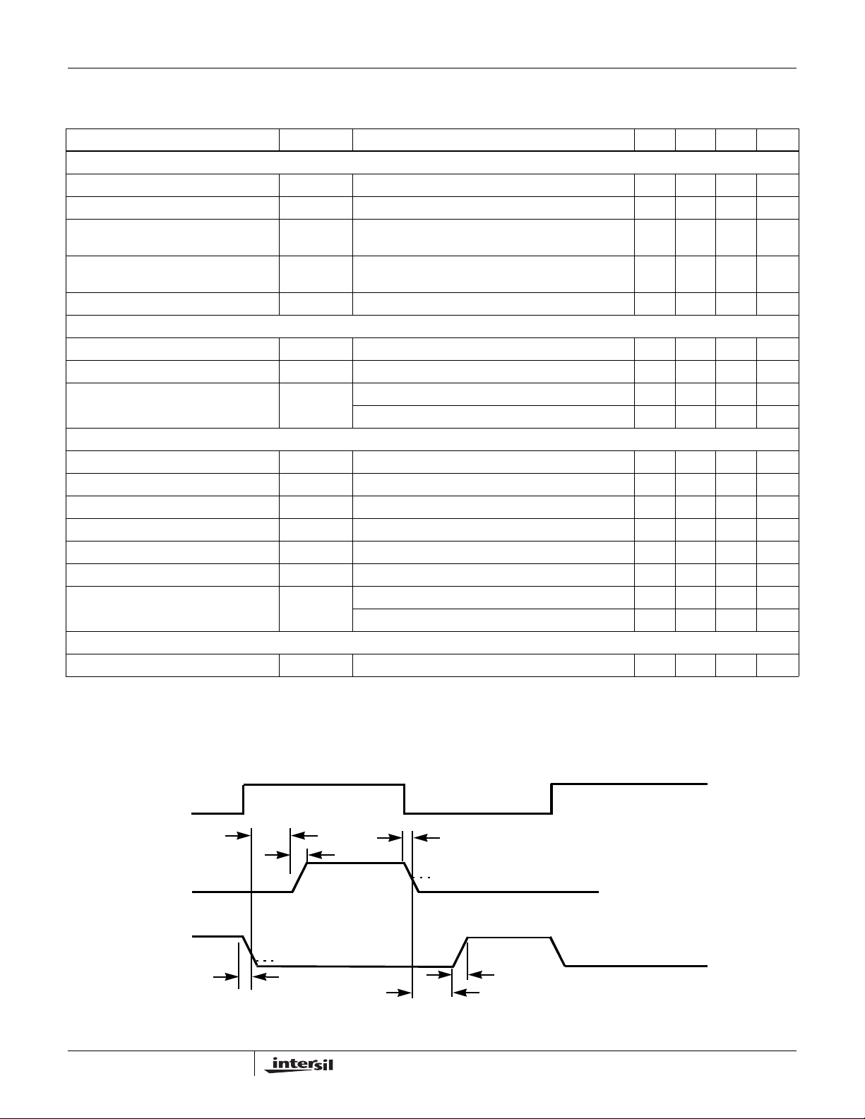
GATE DRIVER SWITCHING TIMING (Note 3) (Refer to “ISL6265 Gate Driver Timing Diagram” on page 8)
UGATE Rise Time t
LGATE Rise Time t
UGATE Fall Time t
LGATE Fall Time t
UGATE Turn-on Propagation Delay t
LGATE Turn-on Propagation Delay t
RU
RL
FU
FL
PDHU
PDHL
PVCC = 5V, 3nF Load - 8.0 - ns
PVCC = 5V, 3nF Load - 8.0 - ns
PVCC = 5V, 3nF Load - 8.0 - ns
PVCC = 5V, 3nF Load - 4.0 - ns
PVCC = 5V, Outputs Unloaded - 36 - ns
PVCC = 5V, Outputs Unloaded - 20 - ns
BOOTSTRAP DIODE
Forward Voltage V
Leakage V
= 5V, Forward Bias Current = 2mA 0.43 0.58 0.67 V
DDP
= 16V - - 1 µA
R
POWER GOOD AND PROTECTION MONITOR
PGOOD Low Voltage V
PGOOD Leakage Current I
OL
OH
PGOOD High After Soft-Start Enable to PGOOD High, V
I
= 4mA - 0.2 0.5 V
PGOOD
P
= 5V -1 - 1 µA
GOOD
= 1.1V 570 700 1010 µs
COREx
PGOOD Low After Fault Fault to PGOOD Low 160 208 250 µs
Undervoltage Threshold U
Overvoltage Threshold O
VH
VHS
V
falls below set-point for 208μs 240 295 350 mV
COREx
VO rising above threshold > 0.5µs 1.770 1.795 1.820 V
OVERCURRENT PROTECTION VDD0 AND VDD1
OCSET Reference Voltage
(V
- V
ISNx
)
ISPx
= 180mV; VIN = 15.5V 5 6.0 7 mV
V
OCSET
OVERCURRENT PROTECTION VDD_NB
OCSET_NB OCP Current RBIAS pin to GND = 117kΩ; Trips after 8 PWM cycles 9.2 10 10.8 µA
7
FN6599.1
May 13, 2009
Page 8
ISL6265
Electrical Specifications VCC = PVCC = 5V , V
at +25°C, unless otherwise specified. T emperature limits est ablished by characterization and are not production
= 12V, TA = -10°C to +100°C; Parameters with MIN and/or MAX limits are 100% tested
IN
tested. (Continued)
PARAMETER SYMBOL TEST CONDITIONS MIN TYP MAX UNITS
OFFSET FUNCTION
OFS Pin Voltage For Droop Enabling V
FB Pin Source Current I
OFS Pin Voltage Threshold for VFIX
Mode and No Droop Operation (Note 3)
OFS Pin Voltage Threshold for SVI Mode
and No Droop Operation (Note 3)
OFS Bias (Note 3) I
V
V
OFS
FB
OFS
OFS
OFS
R
= 240kΩ (OFS pin to GND) 1.18 1.2 1.22 V
OFS
I
= 10µA 9.0 9.9 10.8 µA
OFS
-1.8- V
-4.0- V
1.8V < OFS < VCC - 4.0 - µA
LOGIC INPUTS
ENABLE Low Threshold V
ENABLE High Threshold V
IL(3.3V)
IH(3.3V)
- 1.35 0.9 V
2.0 1.6 - V
ENABLE Leakage Current Logic input is low -1 0 - µA
Logic input is high at 3.3V - 0 1 µA
SVI INTERFACE
PWROK Input Low Threshold - 0.65 0.8 V
PWROK Input High Threshold (Note 3) -0.9- V
SVC, SVD Input HIGH (VIH) 1.05 0.87 - V
SVC, SVD Input LOW (VIL) - 0.68 0.45 V
Schmitt Trigger Input Hysteresis (Note 3) -0.19- V
SVD Low Level Output Voltage 3mA Sink Current - 0.1 0.285 V
SVC, SVD Leakage (Note 3) EN = 0V, SVC, SVD = 0V - < -100 - nA
EN = 5V, SVC, SVD = 1.8V - < -100 - nA
DIFF AMP
Accuracy VSEN = 0.5V to 1.55V; RTN = 0 ±0.1V -2 - 2 mV
NOTES:
3. Limits should be considered typical and are not production tested.
4. Limits established by characterization and are not production tested.
ISL6265 Gate Driver Timing Diagram
PWM
t
PDHU
t
RU
UGATE
LGATE
1V
t
FL
8
1V
t
PDHL
t
FU
t
RL
FN6599.1
May 13, 2009
Page 9
ISL6265
Functional Pin Description
PHASE_NB
VCC
FB_NB
COMP_NB
VSEN_NB
RTN_NB
FSET_NB
RTN1
49
GND
VSEN1
OCSET_NB
PGND_NB
FB_1
VDIFF_1
COMP_1
OFS/VFIXEN
PGOOD
PWROK
SVD
SVC
ENABLE
RBIAS
OCSET
VDIFF_0
FB_0
COMP_0
VW0
VIN
48
47 46 45 44 43 42 41 40 39
1
2
3
4
5
6
7
8
9
10
11
12
13 14 15 16 17 18 19 20 21 22
ISP0
ISN0
RTN0
VSEN0
VCC
The bias supply for the IC’s control circuitry. Connect this pin
to a +5V supply and decouple using a quality 0.1µF ceramic
capacitor.
VIN
Battery supply voltage. It is used for input voltage feed-forward
to improve the input line transient performance.
PVCC
The power supply pin for the internal MOSFET gate drivers
of the ISL6265. Connect this pin to a +5V power supply.
Decouple this pin with a quality 1.0µF ceramic capacitor.
GND
The bias and reference ground for the IC. The GND
connection for the ISL6265 is through the thermal pad on the
bottom of the package.
RBIAS
A 117kΩ resistor from RBIAS to GND set s internal reference
currents. The addition of capacitance to this pin must be
avoided and can create instabilities in operation.
OFS/VFIXEN
A resistor from this pin to GND programs a DC current
source, which generates a positive offset voltage across the
resistor between FB and VDIFF pins. In this case, the OFS
pin voltage is +1.2V and VFIX mode is not enabled. If OFS is
pulled up to +3.3V, VFIX mode is enabled, the DAC decodes
the SVC and SVD inputs to determine the programmed
voltage, and the OFS function is disabled. If OFS is pulled up
to +5V, the OFS function and VFIX mode are disabled.
LGATE_N B
VW1
38 37
23 24
ISP_1
UGATE_ N B
BOOT_NB
36
BOOT_0
35
UGATE_0
34
PHASE_0
33
PGND_0
32
LGATE_0
31
PVCC
30
LGATE_1
29
PGND_1
28
PHASE_1
27
UGATE_1
26
BOOT_1
25
ISN_1
PWROK
System power good input. When this pin is high, the SVI
interface is active and I
is low, the SVC, SVD, and VFIXEN input states determine
the pre-PWROK metal VID or VFIX mode voltage. This pin
must be low prior to the ISL6265 PGOOD output going high
per the AMD SVI Controller Guidelines.
2
C protocol is running. While this pin
PGOOD
Controller power-good open-drain output. This pin is
typically pulled up externally by a 2.0kΩ resistor to +3.3V.
During normal operation, this pin indicates whether all output
voltages are within specified overvoltage and undervoltage
limits and no overcurrent condition is present. If any output
voltage exceeds these limits or a reset event occurs, the pin
is pulled low. This pin is always low prior to the end of
soft-start.
SVC
This pin is the serial VID clock input from the AMD
processor.
SVD
This pin is the serial VID data bidirectional signal to and from
the master device on the AMD processor.
ENABLE
Digital input enable. A high level logic signal on this pin
enables the ISL6265.
FSET_NB
A resistor from this pin to GND programs the switching
frequency of the Northbridge controller (for example,
22.1k ~ 260kHz).
FB_NB
This pin is the output voltage feedback to the inverting input
of the Northbridge controller error amplifier.
COMP_NB
This pin is the output of the Northbridge controller error
amplifier.
VSEN_NB, RTN_NB
Remote Northbridge voltage sense input and return.
Connect isolated traces from these pins to the Northbridge
sense points of the processor.
OCSET_NB
Overcurrent protection selection input for the Northbridge
controller. A resistor from this pin to PHASE_NB sets the OC
trip point.
UGATE_NB
Upper MOSFET gate signal from Northbridge controller.
LGATE_NB
Lower MOSFET gate signal from Northbridge controller.
9
FN6599.1
May 13, 2009
Page 10

ISL6265
PHASE_NB
Switch node of the Northbridge controller. This pin should
connect to the source of the Northbridge channel upper
MOSFET(s).
BOOT_NB
This pin is the upper gate drive supply voltage for the
Northbridge controller. Connect an appropriately sized
ceramic bootstrap capacitor between the BOOT_NB and
PHASE_NB pins. An internal bootstrap diode connected to
the PVCC pin provides the necessary bootstrap charge.
PGND_NB
The return path of the Northbridge controller lower gate
driver. Connect this pin to the source of the lower
MOSFET(s).
OCSET
CORE_0 and CORE_1 common overcurrent protection
selection input. The voltage on this pin sets the (ISPx - ISNx)
voltage limit for OC trip.
VW0, VW1
A resistor from this pin to corresponding COMPx pin
programs the switching frequency (for example, 6.81k ~
300kHz).
COMP0, COMP1
The output of the CORE_0 and CORE_1 controller error
amplifiers respectively. FBx, VDIFFx, and COMPx pins are
tied together through external R-C networks to compensate
the regulator.
Connect ISN0 and ISN1 to the node between the RC sense
elements surrounding the inductor of their respective
channel. Tie the ISP0 and ISP1 pins to the VCORE side of
their corresponding channel’s sense capacitor. These pins
can also be used for discrete resistor sensing.
BOOT0, BOOT1
These pins provide the bias voltage for the corresponding
upper MOSFET drives. Connect these pins to appropriately
chosen external bootstrap capacitors. Internal bootstrap
diodes connected to the PVCC pin provide the necessary
bootstrap charge.
UGATE0, UGATE1
Connect these pins to the corresponding upper MOSFET
gate(s). These pins control the upper MOSFET gate(s) and
are monitored for shoot-through prevention.
LGATE0, LGATE1
Connect these pins to the corresponding lower MOSFET
gate(s).
PHASE0, PHASE1
Switch node of the CORE_0 and CORE_1 controllers.
Connect these pins to the sources of the corresponding
upper MOSFET(s). These pins are the return path for the
upper MOSFET drives.
PGND0, PGND1
The return path of the lower gate driver for CORE_0 and
CORE_1 respectively. Connect these pins to the
corresponding sources of the lower MOSFETs.
FB0, FB1
These pins are the output voltage feedback to the inverting
input of the CORE_0 and CORE_1 error amplifiers.
VDIFF0, VDIFF1
Output of the CORE_0 and CORE_1 differential amplifiers.
VSEN0, RTN0
Inputs to the CORE_0 VR controller precision differential
remote sense amplifier. Connect to the sense pins of the
VDD0_FB[H,L] portion of the processor.
VSEN1, RTN1
Inputs to the CORE_1 VR controller precision differential
remote sense amplifier. Connect to the sense pins of the
VDD1_FB[H,L] portion of the processor. The RTN1 pin is
also used for detection of the VDD_PLANE_STRAP signal
prior to enable.
ISP0, ISN0, ISP1, ISN1
These pins are used for differentially sensing the
corresponding channel output current. The sensed current is
used for channel balancing, protection, and core load line
regulation.
Theory of Operation
The ISL6265 is a flexible multi-output controller supporting
Northbridge and single or dual power planes required by
Class M AMD Mobile CPUs. In dual plane applications, both
core voltage regulators operate single-phase. In uniplane
core applications, the core voltage regulators are configured
to operate as a two-phase regulator. All three regulator
outputs include integrated gate drivers for reduced system
cost and small board area. The regulators provide optimum
steady-state and transient performance for microprocessor
applications. System efficiency is enhanced by idling a
phase in uniplane configurations at low-current and
implementing automatic DCM-mode operation when PSI_L
is asserted to logic low.
The heart of the ISL6265 is the R
Robust Ripple Regulator modulator. The R
combines the best features of fixed frequency PWM and
hysteretic PWM while eliminating many of their
shortcomings. The ISL6265 modulator internally synthesizes
an analog of the inductor ripple current and uses hysteretic
comparators on those signals to establish PWM pulse
widths. Operating on these large-amplitude, noise-free
synthesized signals allows the ISL6265 to achieve lower
3
Technology™, Intersil's
3
modulator
10
FN6599.1
May 13, 2009
Page 11
ISL6265
output ripple and lower phase jitter than either conventional
hysteretic or fixed frequency PWM controllers. Unlike
conventional hysteretic converters, the ISL6265 has an error
amplifier that allows the controller to maintain a 0.5% voltage
regulation accuracy throughout the VID range from 0.75V to
1.55V. Voltage regulation accuracy is slightly wider, ±5mV,
over the VID range from 0.7375V to 0.5V.
The hysteresis window voltage is relative to the error
amplifier output such that load current transients result in
increased switching frequency, which gives the R
3
regulator
a faster response than conventional fixed frequency PWM
controllers. In uniplane configurations, transient load current
is inherently shared between active phases due to the use of
a common hysteretic window voltage. Individual average
phase currents are monitored and controlled to equally
share current among the active phases.
Modulator
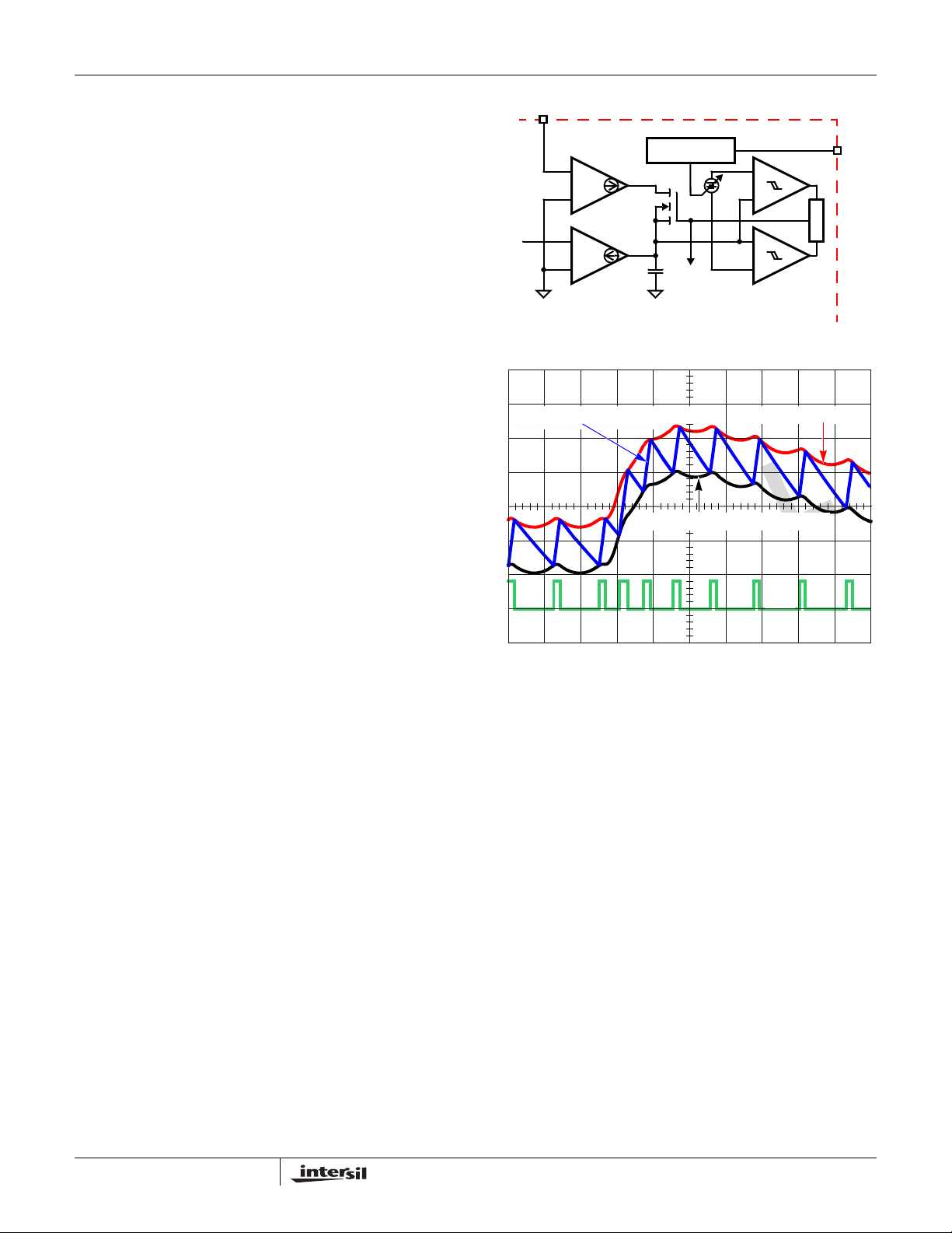
The ISL6265 modulator features Intersil’s R3 technology, a
hybrid of fixed frequency PWM control and variable
frequency hysteretic control (see Figure 5). Intersil’s R
technology can simultaneously affect the PWM switching
frequency and PWM duty cycle in response to input voltage
and output load transients. The R
AC signal V
, which is an analog representation of the
R
3
modulator synthesizes an
output inductor ripple current. The duty-cycle of V
result of charge and discharge current through a ripple
capacitor C
transconductance amplifier g
VO voltages. The positive slope of V
. The current through CR is provided by a
R
that measures the VIN and
m
can be written as
R
determined by Equation 1:
V
RPOSgm
The negative slope of V
()VINV
–()⋅=
OUT
can be written as determined by
R
Equation 2:
V
RNEGgmVOUT
Where g
A window voltage V
amplifier output voltage V
which the ripple voltage V
V
is set by a resistor connected across the FSET and GND
W
pins. The V
comparator in which V
and V
W
PWM pulses being generated as V
V
COMP
⋅=
is the gain of the transconductance amplifier.
m
is referenced with respect to the error
R, VCOMP,
W
and VW signals feed into a window
COMP
, creating an envelope into
COMP
is compared. The amplitude of
R
is the lower threshold voltage
is the higher threshold voltage. Figure 6 shows
traverses the VW and
R
thresholds. The PWM switching frequency is
proportional to the slew rates of the positive and negative
slopes of V
between V
it is inversely proportional to the voltage
R;
W
and V
COMP
.
is the
R
3
(EQ. 1)
(EQ. 2)
.
VIN
PWM FREQUENCY
+
g
mVIN
-
VO
RIPPLE CAPACITOR VOLTAGE C
FIGURE 6. MODULATOR W A VEFORMS DURING LOAD
+
g
mVO
-
FIGURE 5. MODULATOR CIRCUITRY
TRANSIENT
CONTROL
+
C
TO
R
-
PWM
CONTROL
R
ERROR AMPLIFIER VOLTAGE V
-
+
V
W
-
+
PWM
V
-
R
V
COMP
+
WINDOW VOLTAGE V
PWM
ISL6265
FSET
R
Q
S
W
COMP
Initialization
Once sufficient bias is applied to the VCC pin, internal logic
checks the status of critical pins to determine the controller
operation profile prior to ENABLE. These pins include RTN1
which determines single vs two-phase operation and
OFS/VFIXEN for enabling/disabling the SVI interface and core
voltage droop. Depending on the configuration set by these
pins, the controller then checks the state of the SVC and SVD
pins to determine the soft-start target output voltage level.
Power-On Reset
The ISL6265 requires a +5V input supply tied to VCC and
PVCC to exceed a rising power-on reset (POR) threshold
before the controller has sufficient bias to guarantee proper
operation. Once this threshold is reached or exceeded, the
ISL6265 has enough bias to begin checking RTN1,
OFS/VFIXEN, ENABLE, and SVI inputs. Hysteresis between
the rising the falling thresholds assure the ISL6265 will not
inadvertently turn-off unless the bias voltage drops
substantially (see “Electrical Specifications” on page 8).
11
Core Configuration
The ISL6265 determines the core channel requirements of
the CPU based on the state of the RTN1 pin prior to
FN6599.1
May 13, 2009
Page 12
ISL6265
ENABLE. If RTN1 is low prior to ENABLE, both VDD0 and
VDD1 core planes are required. The core controllers operate
as independent single-phase regulators. RTN1 is connected
to the CPU Core1 negative sense point. For single core CPU
designs (uniplane), RTN1 is tied to a +1.8V or greater supply
through a 1kΩ resistor and the connection between RTN1
and CPU Core1 negative sense must be open. Prior to
ENABLE, RTN1 is detected as HIGH and the ISL6265 drives
the core controllers as a two-phase multi-phase regulator.
Dual purpose motherboard designs should include resistor
options to open the CPU Core1 negative sense and connect
the RTN1 pin to a pull-up resistor.
Mode Selection
The OFS/VFIXEN pin selects between the AMD defined
VFIX and SVI modes of operation and enables droop if
desired in SVI mode only. If OFS/VFIXEN is tied to VCC,
then SVI mode with no droop on the core output(s) is
selected. Connected to +3.3V, VFIX mode is active with no
droop on the core output(s). SVI mode with droop is enabled
when OFS/VFIXEN is tied to ground through a resistor sized
4
1
2
3
5
to set the core voltage positive offset. Further information is
provided in “Offset Resistor Selection” on page 17.
Serial VID Interface
The on-board Serial VID Interface (SVI) circuitry allows the
processor to directly control the Core and Northbridge
voltage reference levels within the ISL6265. The SVC and
SVD states are decoded according to the PWROK and
VFIXEN inputs as described in the following sections. The
ISL6265 uses a digital-to-analog converter (DAC) to
generate a reference voltage based on the decoded SVI
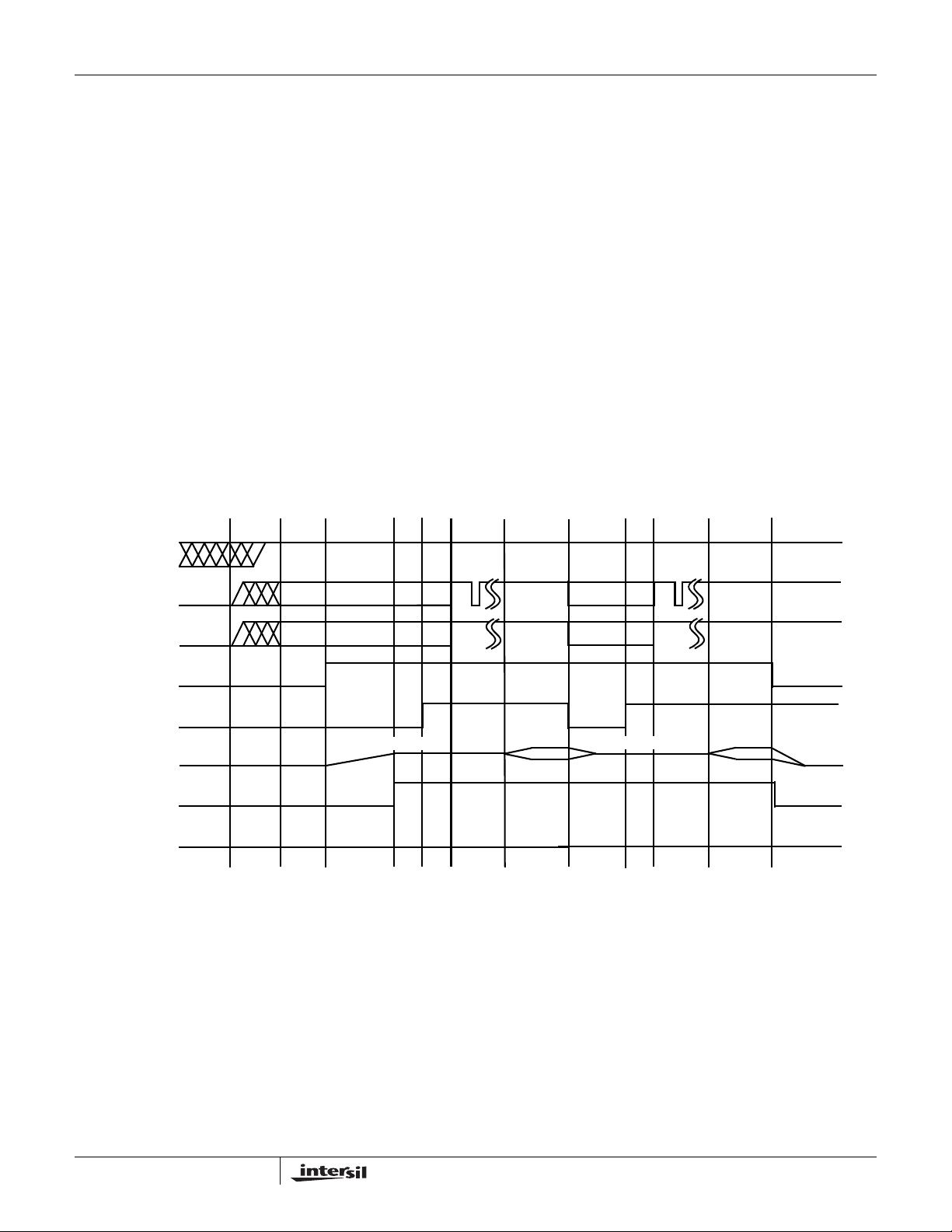
value. See Figure 7 for a simple SVI interface timing
diagram.
Pre-PWROK Metal VID
Assuming the OFS/VFIXEN pin is not tied to +3.3V during
controller configuration, typical motherboard start-up begins
with the controller decoding the SVC and SVD inputs to
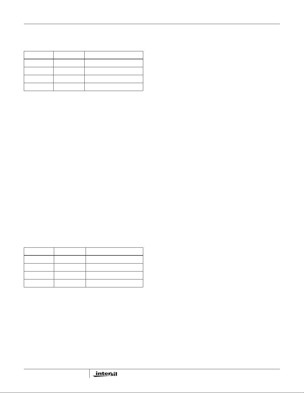
determine the pre-PWROK metal VID setting (see Table 1).
Once the enable input (EN) exceeds the rising enable
6
7 8910 11 12
VCC
SVC
SVD
ENABLE
PWROK
VDD AND VDDNB
VDDPWRGD
(PGOOD)
FIXEN
Interval 1 to 2: ISL6265 waits to POR.
Interval 2 to 3: SVC and SVD are externally set to pre-Metal VID code.
Interval 3 to 4: EN locks core output configuration and pre-Metal VID code. All outputs soft-start to this level.
Interval 4 to 5: PGOOD signal goes HIGH indicating proper operation.
Interval 5 to 6: CPU detects VDDPWRGD high and drives PWROK high to allow ISL6265 to prepare for SVI code.
Interval 6 to 7: SVC and SVD data lines communicate change in VID code.
Interval 7 to 8: ISL6265 responds to VID-ON-THE-FLY code change.
Interval 8 to 9: PWROK is driven low and ISL6265 returns all outputs to pre-PWROK Metal VID level.
Interval 9 to 10: PWROK driven high once again by CPU and ISL6265 prepares for SVI code.
Interval 10 to 11: SVC and SVD data lin es communicate new VID code.
Interval 11 to 12: ISL6265 drives outputs to new VID code level.
Post 12: Enable falls and all internal drivers are tri-stat ed and PGOOD is driven low.
FIGURE 7. SVI INTERFACE TIMING DIAGRAM: TYPICAL PRE-PWROK METAL VID STARTUP
METAL_VID
V_SVI V_SVI
METAL_VID
12
FN6599.1
May 13, 2009
Page 13
ISL6265
threshold, the ISL6265 decodes and locks the decoded
value in an on-board hold register.
TABLE 1. PRE-PWROK METAL VID CODES
SVC SVD OUTPUT VOLTAGE (V)
00 1.1
01 1.0
10 0.9
11 0.8
The internal DAC circuitry begins to ramp Core and
Northbridge planes to the decoded pre-PWROK metal VID
output level. The digital soft-start circuitry ramps the internal
reference to the target gradually at a fixed rate of
approximately 2mV/µs. The controlled ramp of all output
voltage planes reduces in-rush current during the soft-start
interval. At the end of the soft-start interval, the PGOOD
output transitions high indicating all output planes are within
regulation limits.
If the EN input falls below the enable falling threshold, the
ISL6265 tri-states all outputs. PGOOD is pulled low with the
loss of EN. The Core and Northbridge planes will decay
based on output capacitance and load leakage resistance. If
bias to VCC falls below the POR level, the ISL6265
responds in the same manner previously described. Once
VCC and EN rise above their respective rising thresholds,
the internal DAC circuitry re-acquires a pre-PWROK metal
VID code and the controller soft-starts.
VFIX MODE
In VFIX Mode, the SVC and SVD levels fixed external to the
controller through jumpers to either GND or VDDIO. These
inputs are not expected to change. In VFIX mode, the IC
decodes the SVC and SVD states per Table 2.
TABLE 2. VFIXEN VID CODES
SVC SVD OUTPUT VOLTAGE (V)
00 1.4
01 1.2
10 1.0
11 0.8
Once enabled, the ISL6265 begins to soft-start both Core
and Northbridge planes to the programmed VFIX level. The
internal soft-start circuitry slowly ramps the reference up to
the target value. The same fixed internal rate of
approximately 2mV/µs results in a controlled ramp of the
power planes. Once soft-start has ended and all output
planes are within regulation limits, the PGOOD pin
transitions high.
In the same manner described in “Pre-PWROK Metal VID”
on page 12, the POR circuitry impacts the internal driver
operation and PGOOD status.
SVI MODE
Once the controller has successfully soft-started and
PGOOD transitions high, the processor can assert PWROK
to signal the ISL6265 to prepare for SVI commands. The
controller actively monitors the SVI interface for set VID
commands to move the plane voltages to start-up VID
values. Details of the SVI Bus protocol are provided in the
AMD Design Guide for Voltage Regulator Controllers
Accepting Serial VID Codes specification.
Once a set VID command is received, the ISL6265 decodes
the information to determine which output plane is affected
and the VID target required (see Table 3).The internal DAC
circuitry steps the required output plane voltage to the new
VID level. During this time, one or more of the planes could
be targeted. In the event either core voltage plane, VDD0 or
VDD1, is commanded to power-off by serial VID commands,
the PGOOD signal remains asserted. The Northbridge
voltage plane must remain active during this time.
If the PWROK input is de-asserted, then the controller steps
both Core and Northbridge planes back to the stored
pre-PWROK metal VID level in the holding register from
initial soft-start. No attempt is made to read the SVC and
SVD inputs during this time. If PWROK is reasserted, then
the on-board SVI interface waits for a set VID command.
If EN goes low during normal operation, all internal drivers
are tri-stated and PGOOD is pulled low. This event clears
the pre-PWROK metal VID code and forces the controller to
check SVC and SVD upon restart.
A POR event on VCC during normal operation will shutdown
all regulators and PGOOD is pulled low. The pre-PWROK
metal VID code is not retained.
VID-on-the-Fly Transition
Once PWROK is high, the ISL6265 detects this flag and
begins monitoring the SVC and SVD pins for SVI
instructions. The microprocessor will follow the protocol
outlined in the following sections to send instructions for
VID-on-the-Fly transitions. The ISL6265 decodes the
instruction and acknowledges the new VID code. For VID
codes higher than the current VID level, the ISL6265 begins
stepping the required regulator output(s) to the new VID
target with a typical slew rate of 7.5mV/µs, which meets the
AMD requirements.
When the VID codes are lower than the current VID level,
the ISL6265 begins stepping the regulator output to the new
VID target with a typical slew rate of -7.5mV/µs. Both Core
and NB regulators are always in CCM during a down VID
transition. The AMD requirements under these conditions do
not require the regulator to meet the minimum slew rate
specification of -5mV/µs. In either case, the slew rate is not
allowed to exceed 10mV/µs. The ISL6265 does not change
the state of PGOOD (VDDPWRGD in AMD specifications)
when a VID-on-the-fly transition occurs.
13
FN6599.1
May 13, 2009
Page 14

ISL6265
SVI WIRE Protocol
The SVI wire protocol is based on the I2C bus concept. Two
wires (serial clock (SVC) and serial data (SVD)), carry
information between the AMD processor (master) and VR
controller (slave) on the bus. The master initiates and
terminates SVI transactions and drives the clock, SVC,
TABLE 3. SERIAL VID CODES
SVID[6:0] VOLTAGE (V) SVID[6:0] VOLTAGE (V) SVID[6:0] VOLTAGE (V) SVID[6:0] VOLTAGE (V)
000_0000b 1.5500 010_0000b 1.1500 100_0000b 0.7500 110_0000b 0.3500
000_0001b 1.5375 010_0001b 1.1375 100_0001b 0.7375 110_0001b 0.3375*
000_0010b 1.5250 010_0010b 1.1250 100_0010b 0.7250 110_0010b 0.3250*
000_0011b 1.5125 010_0011b 1.1125 100_0011b 0.7125 110_0011b 0.3125*
000_0100b 1.5000 010_0100b 1.1000 100_0100b 0.7000 110_0100b 0.3000*
000_0101b 1.4875 010_0101b 1.0875 100_0101b 0.6875 110_0101b 0.2875*
000_0110b 1.4750 010_0110b 1.0750 100_0110b 0.6750 110_0110b 0.2750*
000_0111b 1.4625 010_0111b 1.0625 100_0111b 0.6625 110_0111b 0.2625 *
000_1000b 1.4500 010_1000b 1.0500 100_1000b 0.6500 110_1000b 0.2500*
000_1001b 1.4375 010_1001b 1.0375 100_1001b 0.6375 110_1001b 0.2375*
000_1010b 1.4250 010_1010b 1.0250 100_1010b 0.6250 110_1010b 0.2250*
000_1011b 1.4125 010_1011b 1.0125 100_1011b 0.6125 110_1011b 0.2125*
000_1100b 1.4000 010_1100b 1.0000 100_1100b 0.6000 110_1100b 0.2000*
000_1101b 1.3875 010_1101b 0.9875 100_1101b 0.5875 110_1101b 0.1875*
000_1110b 1.3750 010_1110b 0.9750 100_1110b 0.5750 110_1110b 0.1750 *
000_1111b 1.3625 010_1111b 0.9625 100_1111b 0.5625 110_1111b 0.1625*
001_0000b 1.3500 011_0000b 0.9500 101_0000b 0.5500 111_0000b 0.1500*
001_0001b 1.3375 011_0001b 0.9375 101_0001b 0.5375 111_0001b 0.1375*
001_0010b 1.3250 011_0010b 0.9250 101_0010b 0.5250 111_0010b 0.1250*
001_0011b 1.3125 011_0011b 0.9125 101_0011b 0.5125 111_0011b 0.1125*
001_0100b 1.3000 011_0100b 0.9000 101_0100b 0.5000 111_0100b 0.1000*
001_0101b 1.2875 011_0101b 0.8875 101_0101b 0.4875* 111_0101b 0.0875*
001_0110b 1.2750 011_0110b 0.8750 101_0110b 0.4750* 111_0110b 0.0750*
001_0111b 1.2625 011_0111b 0.8625 101_0111b 0.4625* 111_0111b 0.0625*
001_1000b 1.2500 011_1000b 0.8500 101_1000b 0.4500* 111_1000b 0.0500*
001_1001b 1.2375 011_1001b 0.8375 101_1001b 0.4375* 111_1001b 0.0375*
001_1010b 1.2250 011_1010b 0.8250 101_1010b 0.4250* 111_1010b 0.0250*
001_1011b 1.2125 011_1011b 0.8125 101_1011b 0.4125* 111_1011b 0.0125*
001_1100b 1.2000 011_1100b 0.8000 101_1100b 0.4000* 111_1100b OFF
001_1101b 1.1875 011_1101b 0.7875 101_1101b 0.3875
001_1110b 1.1750 011_1110b 0.7750 101_1110b 0.3750
001_1111b 1.1625 011_1111b 0.7625 101_1111b 0.3625
NOTE:
*Indicates a VID not required for AMD Family 10h processors.
during a transaction. The AMD processor is always the
master and the voltage regulators are the slaves. The slave
receives the SVI transactions and act s accordingly. Mobil e
SVI wire protocol timing is based on high-speed mode I
See AMD Griffin (Family 11h) processor publications for
additional details.
* 111_1101b OFF
* 111_1110b OFF
* 111_1111b OFF
2
C.
*
14
FN6599.1
May 13, 2009
Page 15
SVC
SVD
54
6
SLAVE ADDRESS PHASE
321
0
ISL6265
7
PSI_L
6
(SEE TABLE 3)
5
4
DATA PHASE
SVID
3
1
2
0
START
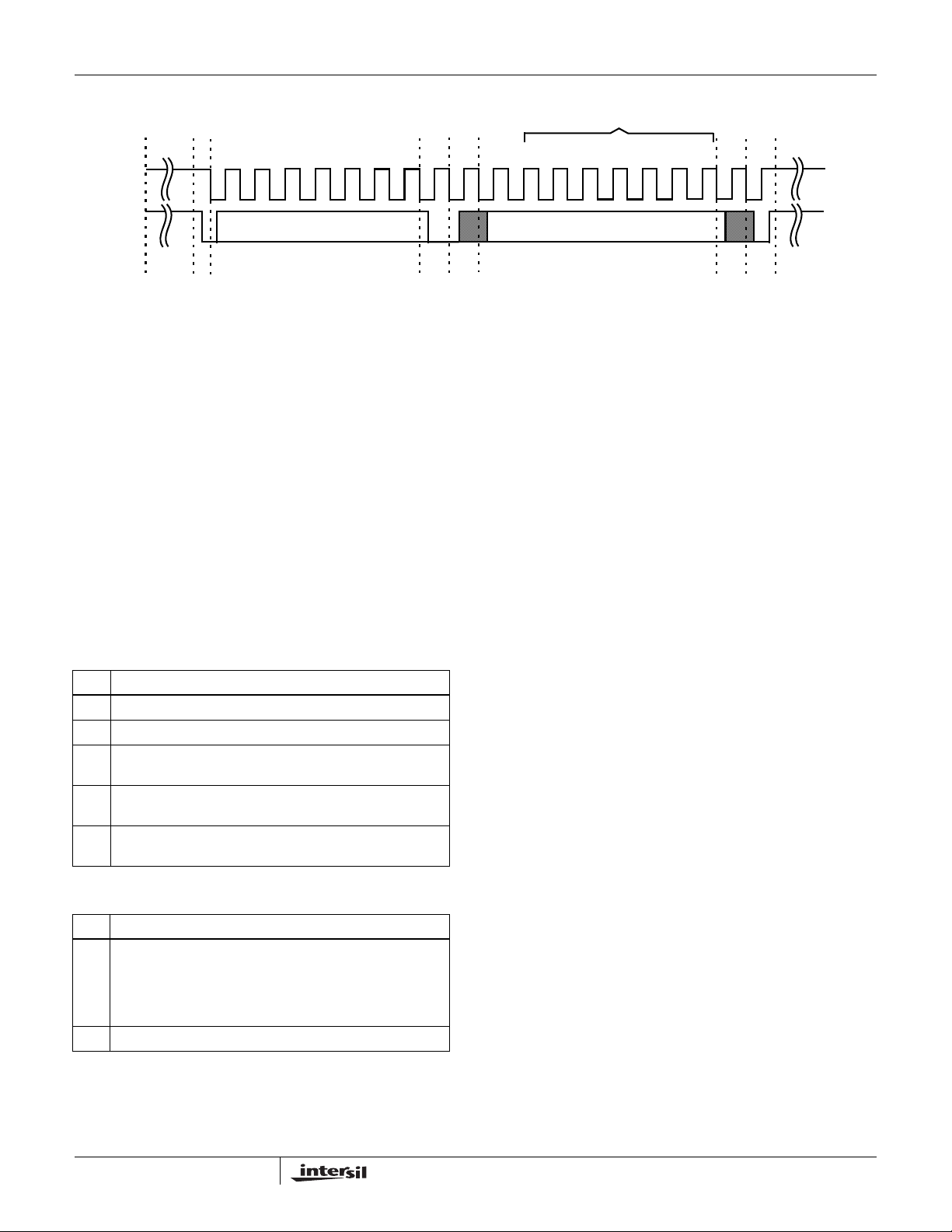
FIGURE 8. SEND BYTE EXAMPLE
SVI Bus Protocol
The AMD processor bus protocol is compliant with SMBus
send byte protocol for VID transactions (see Figure 8).
During a send byte transaction, the processor sends the
start sequence followed by the slave address of the VR for
which the VID command applies. The address byte must be
configured according to Table 4. The processor then sends
the write bit. After the write bit, if the ISL6265 receives a
valid address byte, it sends the acknowledge bit. The
processor then sends the PSI-L bit and VID bits during the
data phase. The Serial VID 8-bit data field encoding is
outlined in Table 5. If ISL6265 receives a valid 8-bit code
during the data phase, it sends the acknowledge bit. Finally,
the processor sends the stop sequence. After the ISL6265
has detected the stop, it can then proceed with the VID-onthe-fly transition.
TABLE 4. SVI SEND BYTE ADDRESS DESCRIPTION
BITS DESCRIPTION
6:4 Always 110b
3 Reserved by AMD for future use
2 VDD1, if set then the following data byte contains the VID for
VDD1
1 VDD0, if set then the following data byte contains the VID for
VID0
0 VDDNB, if set then the following data byte contains the VID
for VIDNB
TABLE 5. SERIAL VID 8-BIT DATA FIELD ENCODING
BITS DESCRIPTION
7 PSI_L:
= 0 means the processor is at an optimal load for the
regulator(s) to enter power-savings mode
= 1 means the processor is not at an optimal load for the
regulator(s) to enter power-saving mode
6:0 SVID[6:0] as defined in Table 3.
ACK
WRITE
ACK
STOP
Operation
After the start-up sequence, the ISL6265 begins regulating
the core and Northbridge output voltages to the pre-PWROK
metal VID programmed. The controller monitors SVI
commands to determine when to enter power-savings mode,
implement dynamic VID changes, and shutdown individual
outputs.
The ISL6265 controls the no-load output voltage of core and
Northbridge output to an accuracy of ±0.5% over-the-range
of 0.75V to 1.5V . A fully differential amplifier implements core
voltage sensing for precise voltage control at the
microprocessor die.
Switching Frequency
The R3 modulator scheme is a variable frequency PWM
architecture. The switching frequency increases during the
application of a load to improve transient performance. It
also varies slightly due to changes in input and output
voltage and output current. This variation is normally less
than 10% in continuous conduction mode.
CORE FREQUENCY SELECTION
A resistor connected between the VW and COMP pins of the
Core segment of the ISL6265 adjusts the switching window
and therefore adjusts the switching frequency. The R
resistor that sets up the switching frequency of the converter
operating in CCM can be determined using Equation 3,
where R
is in kΩ and the switching period is in µs.
FSET
Designs for 300kHz switching frequency would result in a
R
value of 6.81kΩ.
FSET
R
kΩ() Period μs()0.4–()2.33×=
FSET
In discontinuous conduction mode (DCM) the ISL6265 runs
in period stretching mode.
NORTHBRIDGE FREQUENCY SELECTION
The Northbridge switching frequency to programmed by a
resistor connected from the FSET_NB pin to the GND pin.
The approximate PWM switching frequency is written as
shown in Equation 4:
1
-----------------------------------
=
F
SW
⋅
KR
FSETNB
FSET
(EQ. 3)
(EQ. 4)
15
FN6599.1
May 13, 2009
Page 16
ISL6265
Estimating the value of R
FSET_NB
is written as shown in
Equation 5:
1
R
FSET
Where F
-------------------- -
=
⋅
KF
SW
is the PWM switching frequency, R
SW
the programming resistor and K = 1.5 x 10
-10
.
FSET_NB
(EQ. 5)
is
It is recommended that whenever the control loop
compensation network is modified, the switching frequency
should be checked and adjusted by changing R
FSET_NB
if
necessary.
Current Sense
Core and Northbridge regulators feature two different types
of current sense circuits.
CORE CONTINUOUS CURRENT SENSE
The ISL6265 provides for load current to be measured using
either resistors in series with the individual output inductors
or using the intrinsic series resistance of the inductors as
shown in the applications circuits in Figures 2 and 3. The
load current in a particular output is sampled continuously
every switching cycle. During this time the current-sense
amplifier uses the current sense inputs to reproduce a signal
proportional to the inductor current. This sensed current is a
scaled version of the inductor current.
V
IN
UGATE
MOSFET
DRIVER
ISL6265 INTERNAL CIRCUIT
LGATE
CURRENT
SENSE
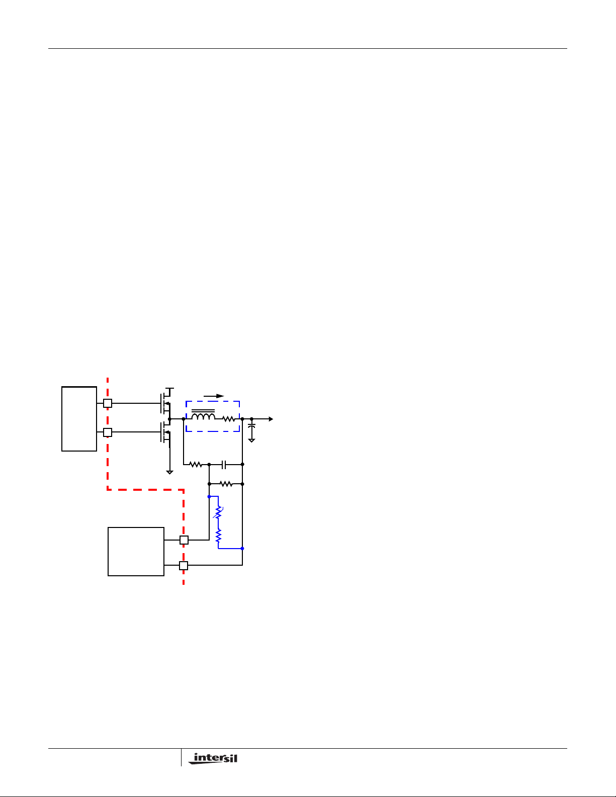
FIGURE 9. DCR SENSING COMPONENTS
Inductor windings have a characteristic distributed
resistance or DCR (Direct Current Resistance). For
simplicity, the inductor DCR is considered as a separate
lumped quantity, as shown in Figure 9. The inductor current,
I
, flowing through the inductor, passes through the DCR.
L
Equation 6 shows the s-domain equivalent voltage, V
across the inductor.
VLs() ILsL DCR+⋅()⋅=
I
L
L
INDUCTOR
VL(s)
+
R
1
ISP
ISN
VC(s)
+
DCR
-
C
1
R
2
R
R
-
NTC
3
V
OUT
C
OUT
OPTIONAL
NTC
NETWORK
,
L
(EQ. 6)
A simple R-C network across the inductor (R
, R2 and C)
1
extracts the DCR voltage, as shown in Equation 7. The
voltage across the sense capacitor, V
proportional to the output current I
sL⋅
⎛⎞
-------------
⎝⎠
-----------------------------------------------------------
s()
V
C
R
⎛⎞
------------------------
⋅⋅1+
s
⎜⎟
R
⎝⎠
1+
DCR
⋅()
1R2
+
1R2
KDCRI
C
1
, can be shown to be
C
, shown in Equation 7.
L
⋅⋅⋅=
L
(EQ. 7)
Where
R
2
---------------------
K
=
R2R1+
(EQ. 8)
Sensing the time varying inductor current accurately
requires that the parallel R-C network time constant match
the inductor L/DCR time constant. If the R-C network
components are selected such that the R-C time constant
matches the inductor L/DCR time constant (see Equation 9),
then V
is equal to the voltage drop across the DCR
C
multiplied by the ratio of the resistor divider, K.
L
-------------
DCR
1R2
---------------------
R
+
1R2
⋅=
C
1
(EQ. 9)
⋅
R
The inductor current sense information is used for current
balance in dual plane applications, overcurrent detection in
core outputs and output voltage droop depending on
controller configuration.
CORE DCR TEMPERATURE COMPENSATION
It may also be necessary to compensate for changes in
inductor DCR due to temperature. DCR shifts due to
temperature cause time constant mismatch, skewing
inductor current accuracy. Potential problems include output
voltage droop and OC trip point, both shifting significantly
from expected levels. The addition of a negative temperature
coefficient (NTC) resistor to the R-C network compensates
for the rise in DCR due to temperature. Typical NTC values
are in the 10kΩ range. A second resistor, R
, in series with
3
the NTC allows for more accurate time-constant and
resistor-ratio matching as the pair of resistors are placed in
parallel with R
next to the inductor for good heat transfer, while R
and C
are placed close to the controller for interference
1
(Figure 9). The NTC resistor must be placed
2
, R2, R3,
1
immunity.
CORE DCR COMPONENT SELECTION FOR DROOP
By adjusting the ratio between inductor DCR drop and the
voltage measured across the sense capacitor, the load line
can be set to any level, giving the converter the correct
amount of droop at all load currents.
Equation 10 shows the relation between droop voltage,
maximum output current (I
sense capacitor voltage at the OC current level, V
I
MAX
------------- -
⋅⋅=
V
DROOP
I
OC
5V
COC,
), OC trip level and current
MAX
C(OC)
(EQ. 10)
.
16
FN6599.1
May 13, 2009
Page 17

ISL6265
AMD specifications do not require droop and provide no load
line guidelines. Tight static output voltage tolerance limits
push acceptable level of droop below a useful level for Griffin
applications. Care must be taken in applications which
implement droop to balance time constant mismatch, sense
capacitor resistor ratio, OC trip and droop equations.
Temperature shifts related to DCR must also be addressed,
as outlined in the previous section.
NORTHBRIDGE CURRENT SENSE
During the off-time following a PHASE transition low, the
Northbridge controller samples the voltage across the lower
MOSFET r
. A ground-referenced amplifier is
DS(ON)
connected to the PHASE node through a resistor,
R
OCSET_NB
voltage drop across the r
. The voltage across R
of the lower MOSFET while
DS(ON)
OCSET_NB
is equal to the
it is conducting. The resulting current into the OCSET_NB
pin is proportional to the inductor current. The sensed
inductor current is used for overcurrent protection and
described in the “Fault Monitoring and Protection” on
page 18. The Northbridge controller does not support output
voltage droop.
Selecting RBIAS For Core Outputs
To properly bias the ISL6265, a reference current is
established by placing a 117kΩ, 1% tolerance resistor from
the RBIAS pin to ground. This will provide a highly accurate,
10µA current source from which OC reference current is
derived.
Care must be taken in layout to place the resistor very close
to the RBIAS pin. A good quality signal ground should be
connected to the opposite end of the R
resistor. Do not
BIAS
connect any other components to this pin as this would
negatively impact performance. Capacitance on this pin
could create instabilities and is to be avoided.
A resistor divider off this pin is used to set the Core side OC
trip level. Additional direction on how to size is provided in
“Fault Monitoring and Protection” on page 18 on how to size
the resistor divider.
Offset Resistor Selection
If the OFS pin is connected to ground through a resistor, the
ISL6265 operates in SVI mode with droop active. The
resistor between the OFS pin and ground sets the positive
Core voltage offset per Equation 11.
1.2V RFB⋅
OFS
----------------------------
=
V
OFS
is the user defined output voltage offset.
OFS
is determined by taking half the total output
OFS
of 1kΩ and a total output droop of 24mV
FB
OFS
(EQ. 11)
of
R
Where V
Typically, V
voltage droop. The resulting value centers the overall output
voltage waveform around the programmed SVID level. For
example, R
would result in an offset voltage of 12mV and a R
100kΩ.
Internal Driver Operation
The ISL6265 features three internal gate-drivers to support
the Core and Northbridge regulators and to reduce solution
size. The drivers include a diode emulation mode, which
helps to improve light-load efficiency.
MOSFET Gate-Drive Outputs
The ISL6265 has internal gate-drivers for the high-side and
low-side N-Channel MOSFETs. The low-side gate-drivers
are optimized for low duty-cycle applications where the
low-side MOSFET conduction losses are dominant,
requiring a low r
resistance is low in order to strongly clamp the gate of the
MOSFET below the V
through the gate at turn-off can be considerable because the
gate charge of a low r
Adaptive shoot-through protection prevents a gate-driver
output from turning on until the opposite gate-driver output
has fallen below approximately 1V.
The high-side gate-driver output voltage is measured across
the UGATE and PHASE pins while the low-side gate-driver
output voltage is measured across the LGATE and PGND
pins. The power for the LGATE gate driver is sourced
directly from the PVCC pin. The power for the UGATE
gate-driver is sourced from a “boot” capacitor connected
across the BOOT and PHASE pins. The boot capacitor is
charged from a 5V bias supply through a “boot diode” each
time the low-side MOSFET turns on, pulling the PHASE pin
low. The ISL6265 has an integrated boot diode connected
from the PVCC pin to the BOOT pin.
Diode Emulation
The ISL6265 implements forced continuous-conductionmode (CCM) at heavy load and diode-emulation-mode (DE)
at light load, to optimize efficiency in the entire load range.
The transition is automatically achieved by detecting the
inductor current when PSI_L is low. If PSI_L is high, the
controller disables DE and forces CCM on both Core and NB
regulators.
Positive-going inductor current flows either from the source
of the high-side MOSFET, or out of the drain of the low-side
MOSFET. Negative-going inductor current flows into the
drain of the low-side MOSFET. When the low-side MOSFET
conducts positive inductor current, the phase voltage is
negative with respect to the GND and PGND pins.
Conversely, when the low-side MOSFET conducts negative
inductor current, the phase voltage is positive with respect to
the GND and PGND pins. The ISL6265 monitors the phase
voltage when the low-side MOSFET is conducting inductor
current to determine the direction of the inductor current.
When the output load current is less than half the inductor
ripple current, the inductor current goes negative. Sinking
the negative inductor through the low-side MOSFET lowers
efficiency by preventing DCM period stretching and allowing
MOSFET. The LGATE pull-down
DS(ON)
at turn-off. The current transient
GS(th)
MOSFET can be large.
DS(ON)
17
FN6599.1
May 13, 2009
Page 18

ISL6265
unnecessary conduction losses. In DE, the ISL6265 Core
regulators automatically enter DCM after the PHASE pin has
detected positive voltage and LGATE was allowed to go
high. The NB regulator enters DCM after the PHASE pin has
detected positive voltage and LGATE was allowed to go high
for eight consecutive PWM switching cycles. The ISL6265
turns off the low-side MOSFET once the phase voltage turns
positive, indicating negative inductor current. The ISL6265
returns to CCM on the following cycle after the PHASE pin
detects negative voltage, indicating that the body diode of
the low-side MOSFET is conducting positive inductor
current.
Efficiency can be further improved with a reduction of
unnecessary switching losses by reducing the PWM
frequency. It is characteristic of the R
3
architecture for the
PWM frequency to decrease while in diode emulation. The
extent of the frequency reduction is proportional to the
reduction of load current. Upon entering DCM, the North
Bridge PWM frequency makes an initial step-reduction
because of a 33% step-increase of the window voltage V
W
Power-Savings Mode
The ISL6265 has two operating modes to optimize efficiency
based on the state of the PSI_L input from the AMD SVI
control signal. When this input is low, the controller expects
to deliver low power and enters a power-savings mode to
improve efficiency in this low power state. The controller’s
operational modes are designed to work in conjunction with
the AMD SVI control signal to maintain the optimal system
configuration for all conditions.
Northbridge And Dual Plane Core
While PSI_L is high, the controller operates all three
regulators in forced CCM. If PSI_L is asserted low by the
SVI interface, the ISL6265 initiates DE in all three regulators.
This transition allows the controller to achieve the highest
possible efficiency over the entire load range for each
output. A smooth transition is facilitated by the R
technology
™
, which correctly maintains the internally
synthesized ripple current throughout mode transitions of
each regulator.
Uniplane Core
In uniplane mode, the ISL6265 Core regulator is in 2-phase
multiphase mode. The controller operates with both phases
fully active, responding rapidly to transients and delivering
the maximum power to the load. When the processor asserts
PSI_L low under reduced load levels, the ISL6265 sheds
one phase to eliminate switching losses associated with the
idle channel. Even with the regulator operating in
single-phase mode, transient response capability is
maintained.
While operating in single-phase DE with PSI_L low, the
lower MOSFET driver switches the lower MO SFET of f at the
point of zero inductor current to prevent discharge current
3
from flowing from the output capacitor bank through the
inductor. In DCM, switching frequency is proportionately
reduced, thus greatly reducing both conduction and
switching loss. In DCM, the switching frequency is defined
by Equation 12.
2
F
DCM
Where F
F
CCM
-------------------
1.33
CCM
2LI
⋅⋅
-------------------------------------
⋅=
2
V
O
V
⎛⎞
O
---------
1
–
⋅
⎜⎟
O
V
⎝⎠
IN
(EQ. 12)
is equivalent to the Core frequency set by
Equation 3.
Fault Monitoring and Protection
The ISL6265 actively monitors Core and Northbridge output
voltages and currents to detect fault conditions. These fault
monitors trigger protective measures to prevent damage to
the processor. One common power good indicator is
provided for linking to external system monitors.
.
Power Good Signal
The power-good pin (PGOOD) is an open-drain logic output
that signals if the ISL6265 is not regulating Core and
Northbridge output voltages within the proper levels or
output current in one or more outputs has exceeded the
maximum current setpoint.
This pin must be tied to a +3.3V or +5V source through a
resistor. During shutdown and soft-start, PGOOD is pulled
low and is released high only after a successful soft-start has
raised Core and Northbridge output voltages within
operating limits. PGOOD is pulled low when an overvoltage,
undervoltage, or overcurrent (OC) condition is detected on
any output or when the controller is disabled by a POR or
forcing enable (EN) low. Once a fault condition is triggered,
the controller acts to protect the processor. The controller
latches off and PGOOD is pulled low. Toggling EN or VCC
initiates a soft-start of all outputs. In the event of an OV, the
controller will initiate a soft-start by toggling EN.
Overcurrent Protection
Core and Northbridge outputs feature two different methods
of current sensing. Core output current sensing is achieved
via inductor DCR or discrete resistor sensing. The
Northbridge controller uses lower MOSFET r
to detect output current.
CORE OC DETECTION
Core outputs feature an OC monitor which compares a
voltage set at the OCSET pin to the voltage measured
across the current sense capacitor, V
. When the voltage
C
across the current sense capacitor exceeds the programmed
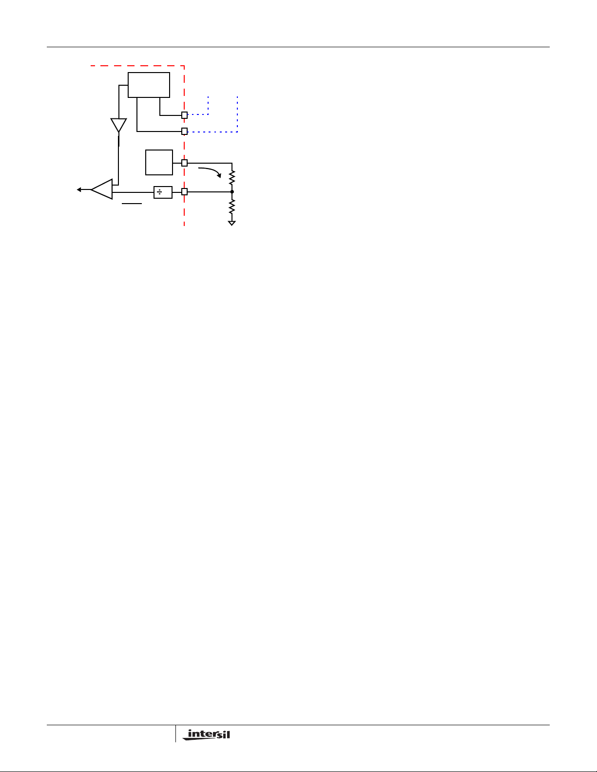
trip level, the comparator signals an OC fault. Figure 10
shows the basic OC functions within the IC.
DS(ON)
sensing
18
FN6599.1
May 13, 2009
Page 19
ISL6265
5 x V
OC TRIP CURRENT
@
C(OC)
OC
FIGURE 10. OC TRIP CIRCUITRY
CURRENT
SENSE
5x
BIAS
CKT
-
+
V
OCSET
6
6
ISL6265
SEE FIGURE 9 FOR
ADDITIONAL DETAIL
ISP
+
V
c
_
ISN
BIAS
1.17V
R
BIAS
V
OCSET
R
OCSET
R
10µA
OCSET
The sense capacitor voltage, VC, will increase as inductor
current rises per Equation 7. When the inductor current rises
to the OC trip level, the voltage across the sense capacitor
will reach a maximum based on the resistor ratio K. This
maximum value, V
, is gained up by a factor of 5 and
C(OC)
compared to the static OC trip level set by the OCSET pin.
The recommended voltage range for V
which sets the resistor divider ratio K, where I
is 6mV to 25mV,
C,OC
is the user-
OC
defined OC trip level (see Equation 13). Typical inductor
DCR values are on the order of 1mΩ which result in more
than enough voltage drop to support this V
V
COC()
----------------------------
=
K
IOCDCR⋅
C,OC
range.
(EQ. 13)
The resistor divider components also impact time-constant
matching, these components need to meet the parallel
combination requirements of Equation 9.
Based on the selected V
trip level is set. The recommended V
level, the required OC monitor
C(OC)
level range will
C(OC)
result in an OC monitor trip level range of 30mV to 125mV
based on the internal gain of 5.
This OC monitor trip level sets the voltage level required at
the OCSET pin to create an OC fault at the user-defined OC
trip level. A resistor divider from the RBIAS pin to ground
with the mid-point connected to OCSET sets the voltage at
the pin (see Figure 10). This voltage is internally divided by 6
and compared with V
. Working backwards, the voltage
C(OC)
required at the OCSET pin to achieve this OC trip level
ranges from 180mV to 0.750mV as defined in Equation 14.
BIAS
(EQ. 14)
and
(EQ. 15)
V
OCSETVCOC()
30⋅=
The resistor divider ratio used to determine the R
R
values is shown in Equation 15.
OCSET
R
OCSET
------------------------------------------------
R
+
OCSETRBIAS
V
-----------------------
=
OCSET
1.17V
The resistor values must also meet the R
requirement
BIAS
that the total series resistance to ground equal 117kΩ.
NORTHBRIDGE OC DETECTION
Northbridge OC sensing is achieved via r
DS(ON)
sensing
across the lower MOSFET. An internal 10µA current source
develops a voltage across R
OCSET_NB
, which is compared
with the voltage developed across the low-side MOSFET as
measured at the PHASE pin. When the voltage drop across
the MOSFET exceeds the voltage drop across the resistor,
an OC event occurs. The OCSET_NB resistor is selected
based on the relationship in Equation 16.
IOCr
⋅
-------------------------------------
R
OCSETNB
Where I
=
is the OC trip level selected for the Northbridge
OC
application and r
DS ON()
10μ A
is the drain-source ON-resistance of
DS(ON)
(EQ. 16)
the lower MOSFET.
OC FAULT RESPONSE
When an OC fault occurs on any combination of outputs,
both Core and Northbridge regulators shutdown and the
driver outputs are tri-stated. The PGOOD signal transitions
low indicating a fault condition. The controller will not attempt
to restart the regulators and the user must toggle either EN
or VCC to clear the fault condition.
Overvoltage Protection
The ISL6265 monitors the individual Core and Northbridge
output voltages using differential remote sense amplifiers.
During an OV, PGOOD is latched low and the upper and
lower MOSFETs are turned off on all outputs. Inductor
current will decay through the MOSFET body diodes. This
condition can be reset by bringing EN low or by bringing
VCC below 3.9V. When these inputs are returned to their
high operating levels, the controller soft-starts.
The ISL6265 features a severe overvoltage (OV) threshold
of 1.8V . If any of the output s exceed this voltage, an OV fault
is immediately triggered. PGOOD is latched low and the
low-side MOSFETs of the offending output(s) are turned on.
The low-side MOSFETs will remain on until the output
voltage is pulled below 0.85V at which time all MOSFETs are
turned off. If the output again rises above 1.8V, the
protection process repeats. This offers protection against a
shorted high-side MOSFET while preventing output voltage
from ringing below ground. The OV is reset by toggling EN
low. OV detection is active at all times that the controller is
enabled including after one of the other faults occurs so that
the processor is protected against high-side MOSFET
leakage while the MOSFETs are commanded off.
Undervoltage Protection
Undervoltage protection is independent of the OC limit. A
fault latches if any of the sensed output voltages are less
than the VID set value by a nominal 295mV for 1ms. The
19
FN6599.1
May 13, 2009
Page 20

ISL6265
PWM outputs turn off both Core and Northbridge internal
drivers and PGOOD goes low.
General Application Design Guide
This design guide is intended to provide a high-level
explanation of the steps necessary to design a single-phase
power converter. It i s assume d that the reader is familiar with
many of the basic skills and techniques referenced in the
following section. In addition to this guide, Intersil provides
complete reference designs that include schematics, bills of
materials, and example board layouts.
Selecting the LC Output Filter
The output inductor and output capacitor bank form a
low-pass filter responsible for smoothing the pulsating
voltage at the phase node. The output filter also must
support the transient energy required by the load until the
controller can respond. Because it has a low bandwidth
compared to the switching frequency, the output filter limits
the system transient response. The output capacitors must
supply or sink load current while the current in the output
inductors increases or decreases to meet the dema n d.
The duty cycle of an ideal buck converter is a function of the
input and the output voltage. This relationship is written as
Equation 17:
V
O
---------
D
=
V
IN
The output inductor peak-to-peak ripple current is written as
Equation 18:
VO1D–()•
------------------------------
=
I
P-P
fSWL•
For this type of application, a typical step-down DC/DC
converter has an I
output load current. The value of I
of 20% to 40% of the maximum DC
P-P
is selected based upon
P-P
several criteria such as MOSFET switching loss, inductor
core loss, and the resistive loss of the inductor winding. The
DC copper loss of the inductor can be estimated by
Equation 19:
2
P
COPPERILOAD
DCR•=
(EQ. 17)
(EQ. 18)
(EQ. 19)
the capacitor. These two voltages are written as shown in
Equation 20:
ΔV
ESRIPP
E• SR=
(EQ. 20)
and Equation 21:
ΔV
=
C
PP
-----------------------------
8COf•
•
SW
(EQ. 21)
I
If the output of the converter has to support a load with high
pulsating current, several capacitors will need to be p aralleled
to reduce the total ESR until the required V
is achieved.
P-P
The inductance of the capacitor can cause a brief voltage dip
if the load transient has an extremely high slew rate. Capacitor
ESL can significantly impact output voltage rippl e. Low
inductance capacitors sh ould be co nsider ed. A cap a citor
dissipates heat as a function of RMS current and frequency.
Be sure that I
is shared by a sufficient quantity of paralleled
P-P
capacitors so that they operate below the maximum rated
RMS current at F
. Take into account that the rated value of
SW
a capacitor can degrade as much as 50% as the DC voltage
across it increases.
Selection of the Input Capacitor
The input capacitors are responsible for sourcing the AC
component of the input current flowing into the upper
MOSFET s. Their RMS current capability must be suf ficient to
handle the AC component of the current drawn by the upper
MOSFETs, which is related to duty cycle and the number of
active phases.
The important parameters for the bulk input capacitance are
the voltage rating and the RMS current rating. For reliable
operation, select bulk capacitors with voltage and current
ratings above the maximum input voltage and capable of
supplying the RMS current required by the switching circuit.
Their voltage rating should be at least 1.25x greater than the
maximum input voltage, while a voltage rating of 1.5x is a
preferred rating. Figure 1 1 is a graph of the input RMS ripple
current, normalized relative to output load current, as a
function of duty cycle for a single-phase regulator that is
adjusted for converter efficiency.
Where I
is the converter output DC current.
LOAD
The copper loss can be significant so attention must be
given to the DCR selection. Another factor to consider when
choosing the inductor is its saturation characteristics at
elevated temperature. A saturated inductor could cause
destruction of circuit components as well as nuisance OCP
faults.
A DC/DC buck regulator must have output capacitance C
into which ripple current I
a corresponding ripple voltage V
can flow. Current I
P-P
across C
P-P
P-P
which is the
O,
O
develops
sum of the voltage drop across the capacitor ESR and of the
voltage change stemming from charge moved in and out of
20
FN6599.1
May 13, 2009
Page 21
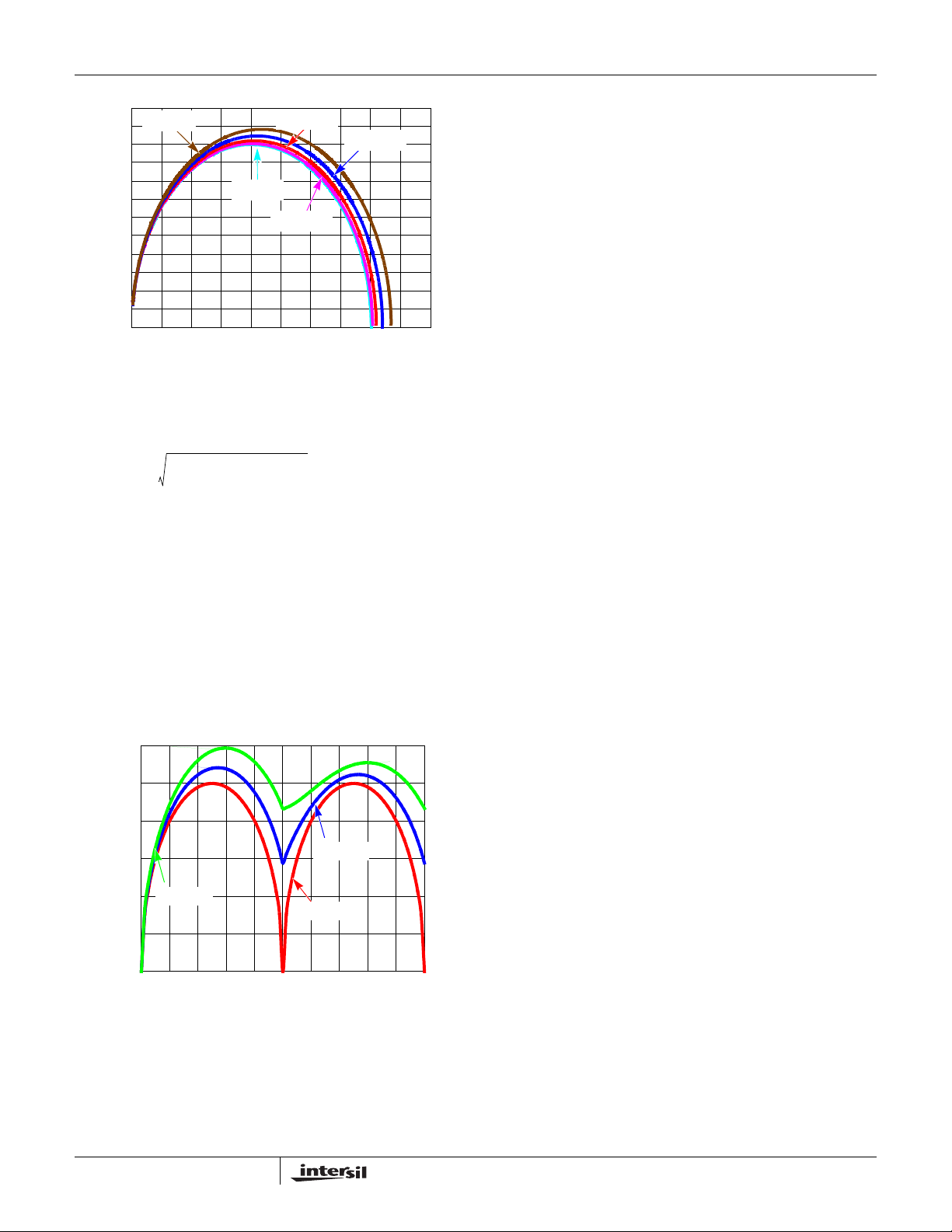
ISL6265
0.60
0.55
0.50
)
O
I
0.45
RMS/
0.40
0.35
0.30
0.25
0.20
0.15
NORMALIZED INPUT RMS
RIPPLE CURRENT (I
0.10
0.05
0
0 0.1 0.2 0.3 0.4 0.5 0.6 0.7 0.8 0.9 1.0
I
P-P,N
= 1
I
P-P,N
DUTY CYCLE (V
= 0
I
I
P-P,N
P-P,N
= 0.50
= 0.25
IN/VO
= 0.75
I
P-P,N
)
FIGURE 11. NORMALIZED RMS INPUT CURRENT FOR
SINGLE PHASE CONVERTER
The normalized RMS current calculation is written as
Equation 22:
I
IN_RMS N,
D1D–()⋅
D
⎛⎞
------
⎝⎠
12
2
⋅+=
I
PP N,
(EQ. 22)
Where:
-I
is the maximum continuous I
MAX
is the ratio of inductor peak-to-peak ripple current
-I
PP,N
to I
MAX
of the converter
LOAD
- D is the duty cycle that is adjusted to take into account
the efficiency of the converter which is written as:
V
O
----------------- -
D
=
VINη⋅
(EQ. 23)
-where η is converter efficiency
Figure 12 provides the same input RMS current information
for two-phase designs.
0.3
)
O
I
0.2
RMS/
I
= 0.5
P-P,N
I
0.1
NORMALIZED INPUT RMS
RIPPLE CURRENT (I
0
FIGURE 12. NORMALIZED RMS INPUT CURRENT FOR
= 0.75
P-P,N
00.4 1.00.2 0.6 0.8
DUTY CYCLE (V
I
P-P,N
IN/VO
= 0
)
2-PHASE CONVERTER
In addition to the bulk capacitance, some low ESL ceramic
capacitance is recommended to decouple between the drain
of the high-side MOSFET and the source of the low-side
MOSFET.
MOSFET Selection and Considerations
The choice of MOSFETs depends on the current each
MOSFET will be required to conduct, the switching
frequency, the capability of the MOSFETs to dissipate heat,
and the availability and nature of heat sinking and air flow.
Typically, a MOSFET cannot tolerate even brief excursions
beyond their maximum drain to source voltage rating. The
MOSFETs used in the power stage of the converter should
have a maximum V
rating that exceeds the sum of the
DS
upper voltage tolerance of the input power source and the
voltage spike that occurs when the MOSFETs switch.
There are several power MOSFET s readily available that are
optimized for DC/DC converter applications. The preferred
high-side MOSFET emphasizes low gate charge so that the
device spends the least amount of time dissipating power in
the linear region. The preferred low-side MOSFET
emphasizes low r
when fully saturated to minimize
DS(ON)
conduction loss.
For the low-side (LS) MOSFET, the power loss can be
assumed to be conductive only and is written as Equation 24:
P
CON_LSILOAD
r⋅
DS ON()_LS
1D–()•≈
(EQ. 24)
2
For the high-side (HS) MOSFET, the its conduction loss is
written as Equation 25:
P
CON_HSILOAD
r•
DS ON()_HS
D•=
(EQ. 25)
2
For the high-side MOSFET, the switching loss is written as
Equation 26:
P
SW_HS
VINI
VALLEYtON
---------------------------------------------------------------- -
2
f•
••
V
INIPEAKtOFF
SW
-------------------------------------------------------------
+=
f•
••
SW
2
(EQ. 26)
Where:
-I
is the difference of the DC component of the
VALLEY
inductor current minus 1/2 of the inductor ri pp l e current
-I
is the sum of the DC component of the inductor
PEAK
current plus 1/2 of the inductor ripple current
is the time required to drive the device into
-t
ON
saturation
is the time required to drive the device into cut-off
-t
OFF
Selecting The Bootstrap Capacitor
All three integrated drivers feature an internal bootstrap
schottky diode. Simply adding an external capacitor across
the BOOT and PHASE pins completes the bootstrap circuit.
The bootstrap function is also designed to prevent the
bootstrap capacitor from overcharging due to the large
negative swing at the PHASE node. This reduces voltage
stress on the BOOT and PHASE pins.
21
FN6599.1
May 13, 2009
Page 22
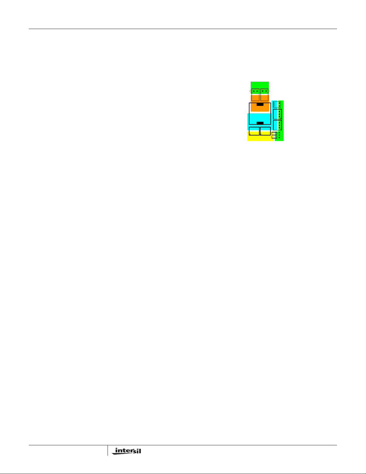
ISL6265
The bootstrap capacitor must have a maximum voltage
rating above PVCC + 4V and its capacitance value is
selected per Equation 27:
Q
g
BOOT
------------------------
≥
ΔV
BOOT
(EQ. 27)
C
Where:
-Q
is the total gate charge required to turn on the
g
high-side MOSFET
- ΔV
, is the maximum allowed voltage decay across
BOOT
the boot capacitor each time the high-side MOSFET is
switched on
As an example, suppose the high-side MOSFET has a total
gate charge Qg, of 25nC at VGS= 5V, and a ΔV
BOOT
of
200mV . The calculated bootstrap capacitance is 0.125µF; for
a comfortable margin, select a capacitor that is double the
calculated capacitance. In this example, 0.22µF will suffice.
Use a low temperature-coefficient ceramic capacitor.
PCB Layout Considerations
Power and Signal Layers Placement on the PCB
As a general rule, power layers should be close together,
either on the top or bottom of the board, with the weak
analog or logic signal layers on the opposite side of the
board. The ground-plane layer should be adjacent to the
signal layer to provide shielding. The ground plane layer
should have an island located under the IC, the
compensation components, and the FSET components. The
island should be connected to the rest of the ground plane
layer at one point.
Component Placement
There are two sets of critical components in a DC/DC
converter; the power components and the small signal
components. The power components are the most critical
because they switch large amount of energy. The small
signal components connect to sensitive nodes or supply
critical bypassing current and signal coupling.
The power components should be placed first and these
include MOSFETs, input and output capacitors, and the
inductor. It is important to have a symmetrical layout for each
power train, preferably with the controller located equidistant
from each power train. Symmetrical layout allows heat to be
dissipated equally across all power trains. Keeping the
distance between the power train and the control IC short
helps keep the gate drive traces short. These drive signals
include the LGATE, UGATE, PGND, PHASE and BOOT.
When placing MOSFET s, try to keep the source of the upper
MOSFETs and the drain of the lower MOSFETs as close as
thermally possible (see Figure 13). Input high-frequency
capacitors should be placed close to the drain of the upper
MOSFETs and the source of the lower MOSFETs. Place the
output inductor and output capacitors between the
MOSFETs and the load. High-frequency output decoupling
capacitors (ceramic) should be placed as close as possible
to the decoupling target (microprocessor), making use of the
shortest connection paths to any internal planes. Place the
components in such a way that the area under the IC has
less noise traces with high dV/dt and di/dt, such as gate
signals and phase node signals.
VIAS TO
GROUND
PLANE
INDUCTOR
HIGH-SIDE
MOSFETS
FIGURE 13. TYPICAL POWER COMPONENT PLACEMENT
GND
VOUT
PHASE
NODE
VIN
OUTPUT
CAPACITORS
SCHOTTKY
DIODE
LOW-SIDE
MOSFETS
INPUT
CAPACITORS
Signal Ground and Power Ground
The bottom of the ISL6265 QFN package is the signal
ground (GND) terminal for analog and logic signals of the IC.
Connect the GND pad of the ISL6265 to the island of ground
plane under the top layer using several vias, for a robust
thermal and electrical conduction path. Connect the input
capacitors, the output capacitors, and the source of the
lower MOSFETs to the power ground plane.
Routing and Connection Details
Specific pins (and the trace routing from them), require extra
attention during the layout process. The following
sub-sections outline concerns by pin name.
PGND PINS
This is the return path for the pull-down of the LGATE
low-side MOSFET gate driver. Ideally, PGND should be
connected to the source of the low-side MOSFET with a
low-resistance, low-inductance path.
VIN PIN
The VIN pin should be connected close to the drain of the
high-side MOSFET, using a low- resistance and
low-inductance path.
VCC PIN
For best performance, place the decoupling capacitor very
close to the VCC and GND pins.
PVCC PIN
For best performance, place the decoupling capacitor very
close to the PVCC and respective PGND pins, preferably on
the same side of the PCB as the ISL6265 IC.
ENABLE AND PGOOD PINS
These are logic signals that are referenced to the GND pin.
Treat as a typical logic signal.
22
FN6599.1
May 13, 2009
Page 23

FB PINS
The input impedance of the FB pin is high, so place the
voltage programming and loop compensation components
close to the COMP, FB, and GND pins keeping the high
impedance trace short.
FSET_NB PIN
This pin requires a quiet environment. The resistor R
FSET
should be placed directly adjacent to this pin. Keep fast
moving nodes away from this pin.
LGATE ROUTING
The LGATE trace has a signal going through it that is both
high dV/dt and di/dt, with high peak charging and
discharging current. Route this trace in parallel with the trace
from the PGND pin. These two traces should be short, wide,
and away from other traces. There should be no other weak
signal traces in proximity with these traces on any layer.
BOOT AND PHASE ROUTING
The signals going through these traces are both high dv/dt
and high di/dt, with high peak charging and discharging
current. Route the UGATE and PHASE pins in parallel with
short and wide traces. There should be no other weak signal
traces in proximity with these traces on any layer.
ISL6265
Copper Size for the Phase Node
The parasitic capacitance and parasitic inductance of the
phase node should be kept very low to minimize ringing. It is
best to limit the size of the PHASE node copper in strict
accordance with the current and thermal management of the
application. An MLCC should be connected directly across
the drain of the upper MOSFET and the source of the lower
MOSFET to suppress the turn-off voltage.
All Intersil U.S. products are manufactured, assembled and tested utilizing ISO9000 quality systems.
Intersil Corporation’s quality certifications can be viewed at www.intersil.com/design/quality
Intersil products are sold by description only. Intersil Corporation reserves the right to make changes in circuit design, software and/or specifications at any time without
notice. Accordingly, the reader is cautioned to verify that data sheets are current before placing orders. Information furnished by Intersil is believed to be accurate and
reliable. However, no responsibility is assumed by Intersil or its subsidiaries for its use; nor for any infringements of patents or other rights of third parties which may result
from its use. No license is granted by implicat ion or oth erwise u nde r any p a tent or p at ent r ights of Intersil or its subsidiaries.
For information regarding Intersil Corporation and its products, see www.intersil.com
23
FN6599.1
May 13, 2009
Page 24
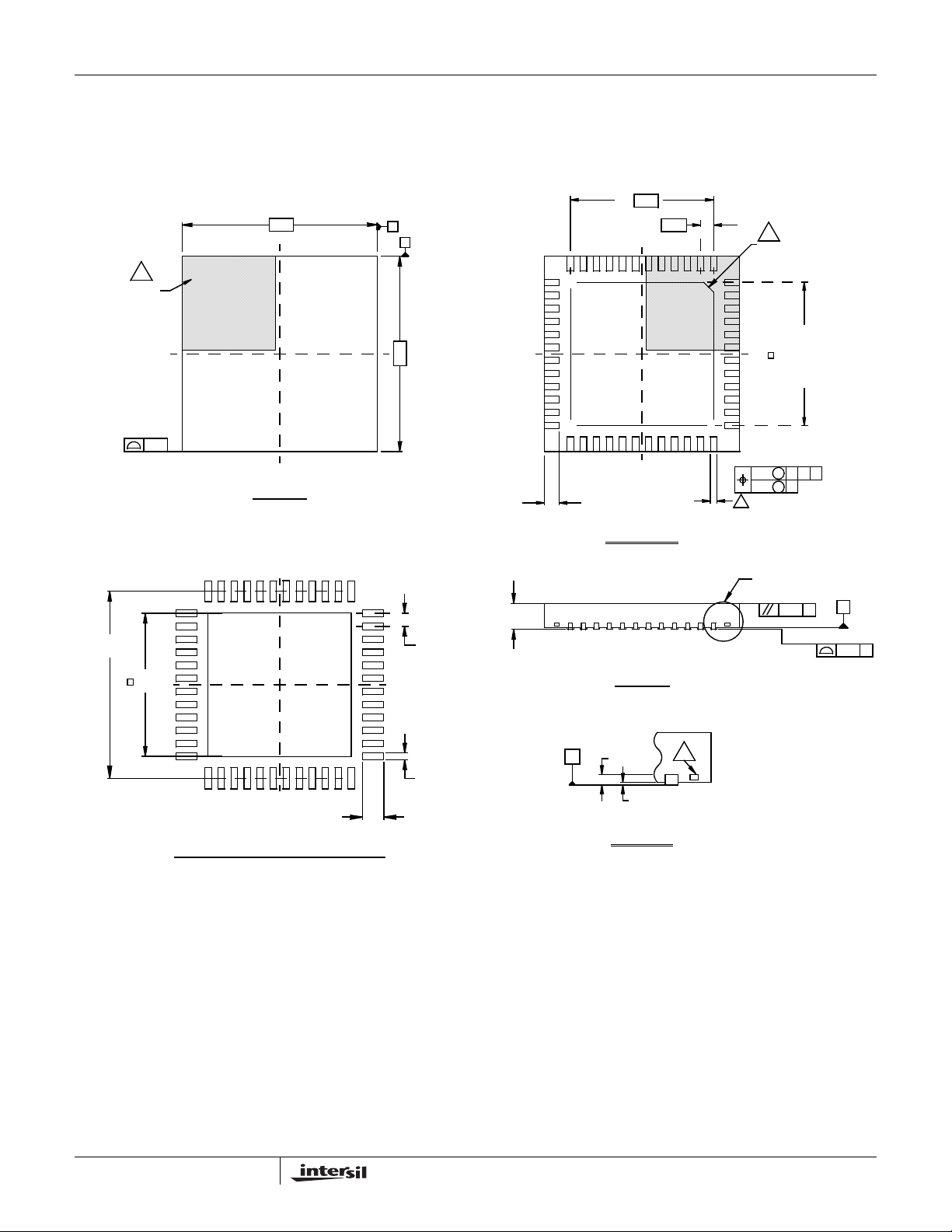
Package Outline Drawing
L48.6x6
48 LEAD THIN QUAD FLAT NO-LEAD PLASTIC PACKAGE
Rev 1, 4/07
6
PIN 1
INDEX AREA
6.00
A
B
ISL6265
4X
4.4
0.40
44X
37
36
48
6
PIN #1 INDEX AREA
1
(4X)
( 5. 75 TYP )
0.15
( 4. 40 )
TOP VIEW
TYPICAL RECOMMENDED LAND PATTERN
6.00
( 44 X 0 . 40 )
( 48X 0 . 20 )
( 48X 0 . 65 )
MAX 0.80
4 .40 ± 0.15
25
24
48X 0.45 ± 0.10
BOTTOM VIEW
SIDE VIEW
0 . 2 REF
C
0 . 00 MIN.
0 . 05 MAX.
5
12
13
4
0.10 CM
0.05 M
48X 0.20
SEE DETAIL "X"
BASE PLANE
AB
C
C
0.10
SEATING PLANE
C
0.08 C
DETAIL "X"
24
NOTES:
Dimensions are in millimeters.1.
Dimensions in ( ) for Reference Only.
2.
Dimensioning and tolerancing conform to AMSE Y14.5m-1994.
3.
Unless otherwise specified, tolerance : Decimal ± 0.05
4.
Dimension b applies to the metallized terminal and is measured
between 0.15mm and 0.30mm from the terminal tip.
Tiebar shown (if present) is a non-functional feature.
5.
The configuration of the pin #1 identifier is optional, but must be
6.
located within the zone indicated. The pin #1 identifier may be
either a mold or mark feature.
FN6599.1
May 13, 2009
 Loading...