

Page 1
®
ISL6262A
Data Sheet December 23, 2008
Two-Phase Core Controller
(Santa Rosa, IMVP-6+)
The ISL6262A is a two-phase buck converter regulator
implementing Intel® IMVP-6+ protocol with embedded gate
drivers. The two-phase buck converter uses two interleaved
channels to effectively double the output voltage ripple
frequency, and thereby reduce output voltage ripple
amplitude with fewer components; lower component cost;
reduced power dissipation; and smaller real estate area.
The heart of the ISL6262A is the patented R
Intersil’s Robust Ripple Regulator modulator. Compared with
the traditional multiphase buck regulator, the R
T echnology™ has the fastest transient response. This is due
to the R
3
modulator commanding variable switching
frequency during a load transient.
Intel® Mobile Voltage Positioning (IMVP) is a smart voltage
regulation technology, which ef fectively reduces power
dissipation in Intel® Pentium processors. T o boost battery
life, the ISL6262A supports DPRSLPVR (deeper sleep),
DPRSTP# and PSI# functions, and maximizes the efficiency
via automatically enabling different phase operation modes.
At heavy load operation of the active mode, the regulator
commands the two phase continuous conduction mode
(CCM) operation. While the PSI# is asserted with medium
load in active mode, the ISL6262A smoothly disables one
phase and operates in one-phase CCM. When the CPU
enters deeper sleep mode, the ISL6262A enables diode
emulation to maximize the efficiency at light load.
For better system power management of the portable
computer, the ISL6262A also provides a CPU power monitor
output. The analog output at the power monitor pin can be
fed into an A/D converter to report instantaneous or average
CPU power.
A 7-bit digital-to-analog converter (DAC) allows dynamic
adjustment of the core output voltage from 0.300V to 1.500V .
A 0.5% system accuracy of the core output voltage
over-temperature is achieved by the ISL6262A.
A unity-gain differential amplifier is provided for remote CPU
die sensing. This allows the voltage on the CPU die to be
accurately measured and regulated per Intel® IMVP-6+
specifications. Current sensing can be realized using either
lossless inductor DCR sensing, or precision resistor sensing.
A single NTC thermistor network thermally compensates the
gain and the time constant of the DCR variations.
3
Technology™,
3
FN6343.1
Features
• Precision Two/One-phase CORE Voltage Regulator
- 0.5% System Accuracy Over-Temperature
- Enhanced Load Line Accuracy
• Internal Gate Driver with 2A Driving Capability
• Dynamic Phase Adding/Dropping
• Microprocessor Voltage Identification Input
- 7-Bit VID Input
- 0.300V to 1.500V in 12.5mV Steps
- Support VID Change On-the-Fly
• Multiple Current Sensing Schemes Supported
- Lossless Inductor DCR Current Sensing
- Precision Resistive Current Sensing
• CPU Power Monitor
• Thermal Monitor
• User Programmable Switching Frequency
• Differential Remote CPU Die Voltage Sensing
• Static and Dynamic Current Sharing
• Overvoltage, Undervoltage, and Overcurrent Protection
• Pb-Free (RoHS Compliant)
Ordering Information
TEMP.
PART NUMBER
(Note)
ISL6262ACRZ ISL6262 ACRZ -10 to +100 48 Ld 7x7 QFN L48.7x7
ISL6262ACRZ-T* ISL6262 ACRZ -10 to +100 48 Ld 7x7 QFN L48.7x7
ISL6262AIRZ ISL6262 AIRZ -40 to +100 48 Ld 7x7 QFN L48.7x7
ISL6262AIRZ-T* ISL6262 AIRZ -40 to +100 48 Ld 7x7 QFN L48.7x7
*Please refer to TB347 for details on reel specifications.
NOTE: These Intersil Pb-free plastic packaged products employ special
Pb-free material sets, molding compounds/die attach materials, and
100% matte tin plate plus anneal (e3 termination finish, which is RoHS
compliant and compatible with both SnPb and Pb-free soldering
operations). Intersil Pb-free products are MSL classified at Pb-free peak
reflow temperatures that meet or exceed the Pb-free requirements of
IPC/JEDEC J STD-020.
PART
MARKING
RANGE
(°C)
PACKAGE
(Pb-Free)
PKG.
DWG. #
1
Intel® is a registered trademark of Intel Corporation. All other trademarks mentioned are the property of their respective owners.
Copyright Intersil Americas Inc. 2008. All Rights Reserved. R
CAUTION: These devices are sensitive to electrostatic discharge; follow proper IC Handling Procedures.
1-888-INTERSIL or 1-888-468-3774
| Intersil (and design) is a registered trademark of Intersil Americas Inc.
3
Technology™ is a trademark of Intersil Americas Inc.
Page 2
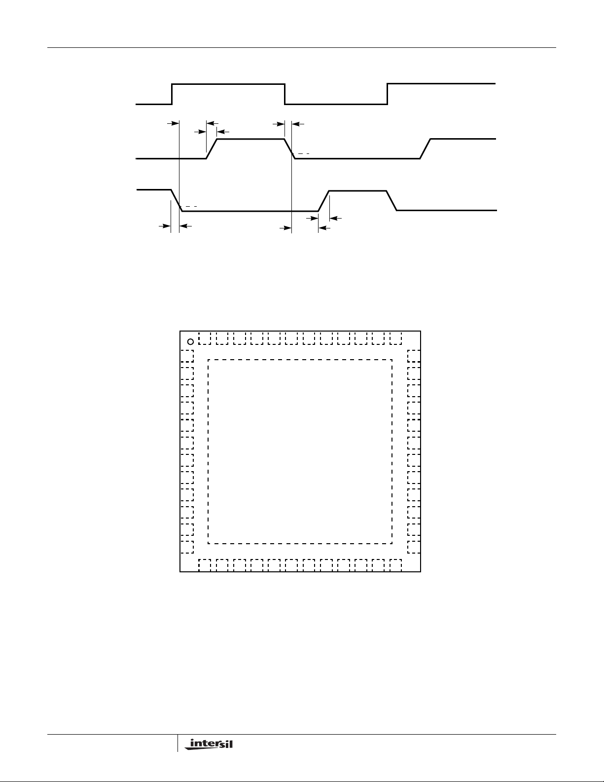
Pinout
ISL6262A
ISL6262A
(48 LD 7x7 QFN)
TOP VIEW
3V3
CLK_EN#
DPRSTP#
DPRSLPVR
VR_ON
VID6
VID5
VID4
VID3
VID2
VID1
48 47 46 45 44 43 42 41 40 39 38 37
VID0
PGOOD
PSI#
PMON
RBIAS
VR_TT#
NTC
SOFT
OCSET
VW
COMP
FB
FB2
1
2
3
4
5
6
7
8
9
10
11
12
13 14 15 16 17 18 19 20 21 22 23 24
RTN
VSEN
VDIFF
DROOP
GND PAD
(BOTTOM)
VO
DFB
VSUM
VIN
GND
36
BOOT1
35
UGATE1
34
PHASE1
33
PGND1
LGATE1
32
31
PVCC
30
LGATE2
29
PGND2
PHASE2
28
UGATE2
27
BOOT2
26
NC
25
VDD
ISEN2
ISEN1
2
FN6343.1
December 23, 2008
Page 3
ISL6262A
Absolute Maximum Ratings Thermal Information
Supply Voltage, VDD. . . . . . . . . . . . . . . . . . . . . . . . . . . -0.3 to +7V
Battery Voltage, VIN. . . . . . . . . . . . . . . . . . . . . . . . . . . . . . . . . +28V
Boot Voltage (BOOT). . . . . . . . . . . . . . . . . . . . . . . . . .-0.3V to +33V
Boot to Phase Voltage (BOOT to PHASE . . . . . . -0.3V to +7V (DC)
-0.3V to +9V (<10ns)
Phase Voltage (PHASE) . . . . . . . . . -7V (<20nS Pulse Width, 10µJ)
UGATE Voltage (UGATE) . . . . . . . . . . PHASE -0.3V (DC) to BOOT
. . . . . . . . . . . . . PHASE-5V (<20nS Pulse Width, 10µJ) to BOOT
LGATE Voltage (LGATE) . . . . . . . . . . . . -0.3V (DC) to (VDD +0.3V)
. . . . . . . . . . . . . .-2.5V (<20nS Pulse Width, 5µJ) to (VDD +0.3V)
All Other Pins. . . . . . . . . . . . . . . . . . . . . . . . . .-0.3V to (VDD +0.3V)
Open Drain Outputs, PGOOD, VR_TT# . . . . . . . . . . . . -0.3 to +7V
CAUTION: Do not operate at or near the maximum ratings listed for extended periods of time. Exposure to such conditions may adversely impact product reliability and
result in failures not covered by warranty.
NOTES:
is measured in free air with the component mounted on a high effective thermal conductivity test board with “direct attach” features. See
1. θ
JA
Tech Brief TB379.
2. For θ
, the “case temp” location is the center of the exposed metal pad on the package underside.
JC
Thermal Resistance (Typical)
θJA
°C/W θJC°C/W
QFN Package (Notes 1, 2). . . . . . . . . . 29 4.5
Maximum Storage Temperature Range. . . . . . . . . -65°C to +150°C
Maximum Junction Temperature . . . . . . . . . . . . . . . . . . . . . +150°C
Pb-free reflow profile . . . . . . . . . . . . . . . . . . . . . . . . . .see link below
http://www.intersil.com/pbfree/Pb-FreeReflow.asp
Recommended Operating Conditions
Supply Voltage, VDD. . . . . . . . . . . . . . . . . . . . . . . . . . . . . +5V ±5%
Battery Voltage, VIN . . . . . . . . . . . . . . . . . . . . . . . . . . . +5V to 25V
Ambient Temperature
Commercial . . . . . . . . . . . . . . . . . . . . . . . . . . . . -10°C to +100°C
Industrial. . . . . . . . . . . . . . . . . . . . . . . . . . . . . . . -40°C to +100°C
Junction Temperature
Commercial . . . . . . . . . . . . . . . . . . . . . . . . . . . . -10°C to +125°C
Industrial. . . . . . . . . . . . . . . . . . . . . . . . . . . . . . . -40°C to +125°C
Electrical Specifications V
= 5V, TA = -40°C to +100°C, unless otherwise specified. Parameters with MIN and/or MAX limits are 100%
DD
tested at +25°C, unless otherwise specified. Temperature limits established by characterization and are not
production tested.
PARAMETER SYMBOL TEST CONDITIONS MIN TYP MAX UNITS
INPUT POWER SUPPLY
+5V Supply Current I
VDD
VR_ON = 3.3V 3.6 4.1 mA
VR_ON = 0V 1 µA
+3.3V Supply Current I
Battery Supply Current at VIN pin I
3V3
VIN
POR (Power-On Reset) Threshold POR
POR
No load on CLK_EN# 1 µA
VR_ON = 0V, VIN = 25V 1 µA
VDD Rising 4.35 4.5 V
r
VDD Falling 4.0 4.15 V
f
SYSTEM AND REFERENCES
System Accuracy %Error
(V
CC_CORE
ISL6262ACRZ
No load, closed loop, active mode,
T
)
= 0°C to +100°C, VID = 0.75 to 1.5V -0.5 0.5 %
A
VID = 0.5 to 0.7375V -8 8 mV
VID = 0.3 to 0.4875V -15 15 mV
System Accuracy %Error
(V
CC_CORE
ISL6262AIRZ
No load, closed loop, active mode,
T
)
= -40°C to +100°C, VID = 0.75 to 1.5V
A
-0.8 0.8 %
VID = 0.5 to 0.7375V -10 10
VID = 0.3 to 0.4875V 18 18 mV
Droop Amplifier Offset 0.3 0.3
Voltage R
R
BIAS
Boot Voltage V
Maximum Output Voltage V
V
RBIAS
BOOT
CC_CORE
(max)
CC_CORE
R
= 147kΩ 1.45 1.47 1.49 V
RBIAS
1.188 1.2 1.212 V
VID = [0000000] 1.5 V
VID = [1100000] 0.3 V
(min)
VID Off State VID = [1111111] 0 V
3
FN6343.1
December 23, 2008
Page 4
ISL6262A
Electrical Specifications V
= 5V, TA = -40°C to +100°C, unless otherwise specified. Parameters with MIN and/or MAX limits are 100%
DD
tested at +25°C, unless otherwise specified. Temperature limits established by characterization and are not
production tested. (Continued)
PARAMETER SYMBOL TEST CONDITIONS MIN TYP MAX UNITS
CHANNEL FREQUENCY
R
Nominal Channel Frequency f
SW
= 6.9kΩ, 2 channel operation,
FSET
V
= 2V
COMP
285 300 315 kHz
Adjustment Range 100 500 kHz
AMPLIFIERS
Droop Amplifier Offset -0.3 0.3 mV
Error Amp DC Gain A
V0
Error Amp Gain-Bandwidth Product GBW C
Error Amp Slew Rate SR C
FB Input Current I
IN(FB)
= 20pF 18 MHz
L
= 20pF 5 V/µs
L
90 dB
10 150 nA
ISEN
Imbalance Voltage 2mV
Input Bias Current 20 nA
SOFT-START CURRENT
Soft-Start Current I
Soft Geyserville Current I
Soft Deeper Sleep Entry Current I
Soft Deeper Sleep Exit Current I
Soft Deeper Sleep Exit Current I
SS
GV
C4
C4EA
C4EB
|SOFT - REF|>100mV ±180 ±205 ±230 µA
DPRSLPVR = 3.3V -47 -42 -37 µA
DPRSLPVR = 3.3V 37 42 47 µA
DPRSLPVR = 0V 180 205 230 µA
-47 -42 -37 µA
GATE DRIVER DRIVING CAPABILITY
UGATE Source Resistance R
UGATE Source Current I
UGATE Sink Resistance R
UGATE Sink Current I
LGATE Source Resistance R
LGATE Source Current I
LGATE Sink Resistance R
LGATE Sink Current I
UGATE to PHASE Resistance R
SRC(UGATE)
SRC(UGATE)VUGATE_PHASE
SNK(UGATE)
SNK(UGATE)VUGATE_PHASE
SRC(LGATE)
SRC(LGATE)
SNK(LGATE)
SNK(LGATE)
p(UGATE)
500mA Source Current 1 1.5 Ω
= 2.5V 2 A
500mA Sink Current 1 1.5 Ω
= 2.5V 2 A
500mA Source Current 1 1.5 Ω
V
= 2.5V 2 A
LGATE
500mA Sink Current 0.5 0.9 Ω
V
= 2.5V 4 A
LGATE
1kΩ
GATE DRIVER SWITCHING TIMING (refer to “ISL6262A Gate Driver Timing Diagram” on page 6)
UGATE Rise Time t
LGATE Rise Time t
UGATE Fall Time t
LGATE Fall Time t
UGATE Turn-on Propagation Delay t
LGATE Turn-on Propagation Delay t
RU
RL
FU
FL
PDHU
PDHU
PVCC= 5V, 3nF Load 8.0 ns
PVCC= 5V, 3nF Load 8.0 ns
PVCC= 5V, 3nF Load 8.0 ns
PVCC= 5V, 3nF Load 4.0 ns
PVCC= 5V, Outputs Unloaded 30 ns
PVCC= 5V, Outputs Unloaded 15 ns
BOOTSTRAP DIODE
Forward Voltage V
Leakage V
= 5V, Forward Bias Current = 2mA 0.43 0.58 0.72 V
DDP
= 16V 1 µA
R
POWER GOOD and PROTECTION MONITOR
I
PGOOD Low Voltage V
PGOOD Leakage Current I
OL
OH
= 4mA 0.26 0.4 V
PGOOD
P
= 3.3V -1 1 µA
GOOD
4
FN6343.1
December 23, 2008
Page 5
ISL6262A
Electrical Specifications V
= 5V, TA = -40°C to +100°C, unless otherwise specified. Parameters with MIN and/or MAX limits are 100%
DD
tested at +25°C, unless otherwise specified. Temperature limits established by characterization and are not
production tested. (Continued)
PARAMETER SYMBOL TEST CONDITIONS MIN TYP MAX UNITS
PGOOD Delay t
Overvoltage Threshold O
Severe Overvoltage Threshold O
pgd
VH
VHS
OCSET Reference Current I (R
CLK_EN# Low to PGOOD High 6.3 7.6 8.9 ms
VO rising above setpoint >1ms 160 200 240 mV
VO rising above setpoint >0.5µs 1.675 1.7 1.725 V
) = 10µA 9.8 10 10.2 µA
BIAS
OC Threshold Offset DROOP rising above OCSET >120µs -3.5 3.5 mV
Current Imbalance Threshold Difference between ISEN1 and ISEN2 >1ms 9 mV
Undervoltage Threshold
(VDIFF-SOFT)
UV
f
VO falling below setpoint for >1ms -360 -300 -240 mV
LOGIC INPUTS
VR_ON, DPRSLPVR Input Low V
VR_ON, DPRSLPVR Input High V
Leakage Current of VR_ON I
Leakage Current of DPRSLPVR I
IL_DPRSLP(3.3V)
I
IH_DPRSLP(3.3V)
DAC(VID0-VID6), PSI# and
DPRSTP# Input Low
DAC(VID0-VID6), PSI# and
DPRSTP# Input High
Leakage Current of DAC(VID0VID6), PSI# and DPRSTP#
IL(3.3V)
IH(3.3V)
IL(3.3V)
I
IH(3.3V)
V
IL(1V)
V
IH(1V)
I
IL(1V)
I
IH(1V)
2.3 V
Logic input is low -1 0 µA
Logic input is high at 3.3V 0 1 µA
DPRSLPVR input is low -1 0 µA
DPRSLPVR input is high at 3.3V 0.45 1 µA
0.7 V
Logic input is low -1 0 µA
Logic input is high at 1V 0.45 1 µA
1V
0.3 V
THERMAL MONITOR
NTC Source Current NTC = 1.3V 53 60 67 µA
Over-Temperature Threshold V(NTC) falling 1.18 1.2 1.22 V
VR_TT# Low Output Resistance R
TT
I = 20mA 6.5 9 Ω
POWER MONITOR
PMON Output Voltage Range V
PMON Maximum Voltage V
PMON Sourcing Current I
PMON Sinking Current I
pmon
pmonmax
sc_pmon
sk_pmon
Maximum Current Sinking Capability (see Figure 31) PMON/
PMON Impedance When PMON is within its sourcing/sinking
VSEN = 1.2V, Droop - VO= 80mV 1.638 1.680 1.722 V
VSEN = 1V, Droop - V
= 20mV 0.308 0.350 0.392 V
O
2.8 3.0 V
VSEN = 1V, Droop - VO= 50mV 2 mA
VSEN = 1V, Droop - VO= 50mV 2 mA
250Ω
PMON/
180Ω
PMON/
130Ω
7 Ω
current range (Established by
characterization)
CLK_EN# OUTPUT LEVELS
CLK_EN# High Output Voltage V
CLK_EN# Low Output Voltage V
OH
OL
3V3 = 3.3V, I = -4mA 2.9 3.1 V
I
CLK_EN#
= 4mA 0.26 0.4 V
A
5
FN6343.1
December 23, 2008
Page 6
ISL6262A Gate Driver Timing Diagram
PWM
t
PDHU
UGATE
t
RU
ISL6262A
t
FU
1V
LGATE
t
FL
1V
Functional Pin Description
PSI#
PMON
RBIAS
NTC
SOFT
VW
1
2
3
4
5
6
7
8
9
PGOOD
VR_TT#
OCSET
t
t
PDHL
3V3
CLK_EN#
DPRSTP#
DPRSLPVR
VR_ON
VID6
VID5
48 47 46 45 44 43 42 41 40 39 38 37
GND PAD
(BOTTOM)
RL
VID4
VID3
VID2
VID1
VID0
36
BOOT1
35
UGATE1
34
PHASE1
33
PGND1
LGATE1
32
31
PVCC
30
LGATE2
29
PGND2
PHASE2
28
COMP
FB
FB2
6
10
11
12
13 14 15 16 17 18 19 20 21 22 23 24
VDIFF
DROOP
RTN
VSEN
VO
DFB
VSUM
VIN
GND
UGATE2
27
BOOT2
26
NC
25
VDD
ISEN2
ISEN1
FN6343.1
December 23, 2008
Page 7

ISL6262A
PGOOD - Power good open-drain output. Connect
externally with 680Ω to VCCP or 1.9kΩ to 3.3V.
PSI# - Current indicator input. When asserted low, indicates
a reduced load-current condition and initiates single-phase
operation.
PMON - Analog output. PMON is proportional to the product
of Vsen and droop voltage.
RBIAS - 147k resistor to GND sets internal current
reference.
VR_TT# - Thermal overload output indicator with open-drain
output. Over-temperature pull-down resistance is 10Ω.
NTC - Thermistor input to VRTT# circuit and a 60µA current
source is connected internally to this pin.
SOFT - A capacitor from this pin to GND sets the maximum
slew rate of the output voltage. SOFT is the non-inverting
input of the error amplifier.
OCSET - Overcurrent set input. A resistor from this pin to
VO sets DROOP voltage limit for OC trip. A 10µA current
source is connected internally to this pin.
VW - A resistor from this pin to COMP programs the
switching frequency (for example, 6.82kΩ ≅ 300kHz).
COMP - This pin is the output of the error amplifier.
FB - This pin is the inverting input of error amplifier.
ISEN1 - Individual current sharing sensing for Channel 1.
N/C - Not connected. Grounding this pin to signal ground in
the practical layout.
BOOT2 - This pin is the upper gate driver supply voltage for
phase 2. An internal boot strap diode is connected to the
PVCC pin.
UGATE2 - Upper MOSFET gate signal for phase 2.
PHASE2 - The phase node of phase 2. Connect this pin to
the source of the Channel 2 upper MOSFET.
PGND2 - The return path of the lower gate driver for
phase 2.
LGATE2 - Lower-side MOSFET gate signal for phase 2.
PVCC - 5V power supply for gate drivers.
LGATE1 - Lower-side MOSFET gate signal for phase 1.
PGND1 - The return path of the lower gate driver for
phase 1.
PHASE1 - The phase node of phase 1. Connect this pin to
the source of the Channel 1 upper MOSFET.
UGATE1 - Upper MOSFET gate signal for phase 1.
BOOT1 - This pin is the upper-gate-driver supply voltage for
phase 1. An internal boot strap diode is connected to the
PVCC pin.
FB2 - There is a switch between FB2 pin and the FB pin.
The switch is closed in single-phase operation and is
opened in two phase operation. The components connecting
to FB2 are to adjust the compensation in single phase
operation to achieve optimum performance.
VDIFF - This pin is the output of the differential amplifier.
VSEN - Remote core voltage sense input.
RTN - Remote core voltage sense return.
DROOP - Output of the droop amplifier. The voltage level on
this pin is the sum of V
and the droop voltage.
O
DFB - Inverting input to droop amplifier.
VO - An input to the IC that reports the local output voltage.
VSUM - This pin is connected to the summation junction of
channel current sensing.
VIN - Battery supply voltage. It is used for input voltage
feed-forward to improve input line transient performance.
GND - Signal ground. Connect to local controller ground.
VDD - 5V control power supply.
ISEN2 - Individual current sharing sensing for Channel 2. If
ISEN2 is pulled to 5V, phase 2’s gate signals are disabled.
ISL6262A is then configured in always-1-phase mode.
VID0, VID1, VID2, VID3, VID4, VID5, VID6 - VID input with
VID0 is the least significant bit (LSB) and VID6 is the most
significant bit (MSB).
VR_ON - Digital enable input. A logic high signal on this pin
enables the regulator.
DPRSLPVR - Deeper sleep enable signal. A logic high
signal on this pin indicates the micro-processor is in
deeper-sleep mode and also indicates a slow C4 entry or
exit rate with 41µA discharging or charging the SOFT
capacitor.
DPRSTP# - Deeper sleep slow wake up signal. A logic low
signal on this pin indicates the micro-processor is in
deeper-sleep mode.
CLK_EN# - Digital output for system clock. Goes active 13
clks after V
is within 10% of Boot voltage.
core
3V3 - 3.3V supply voltage for CLK_EN#.
7
FN6343.1
December 23, 2008
Page 8
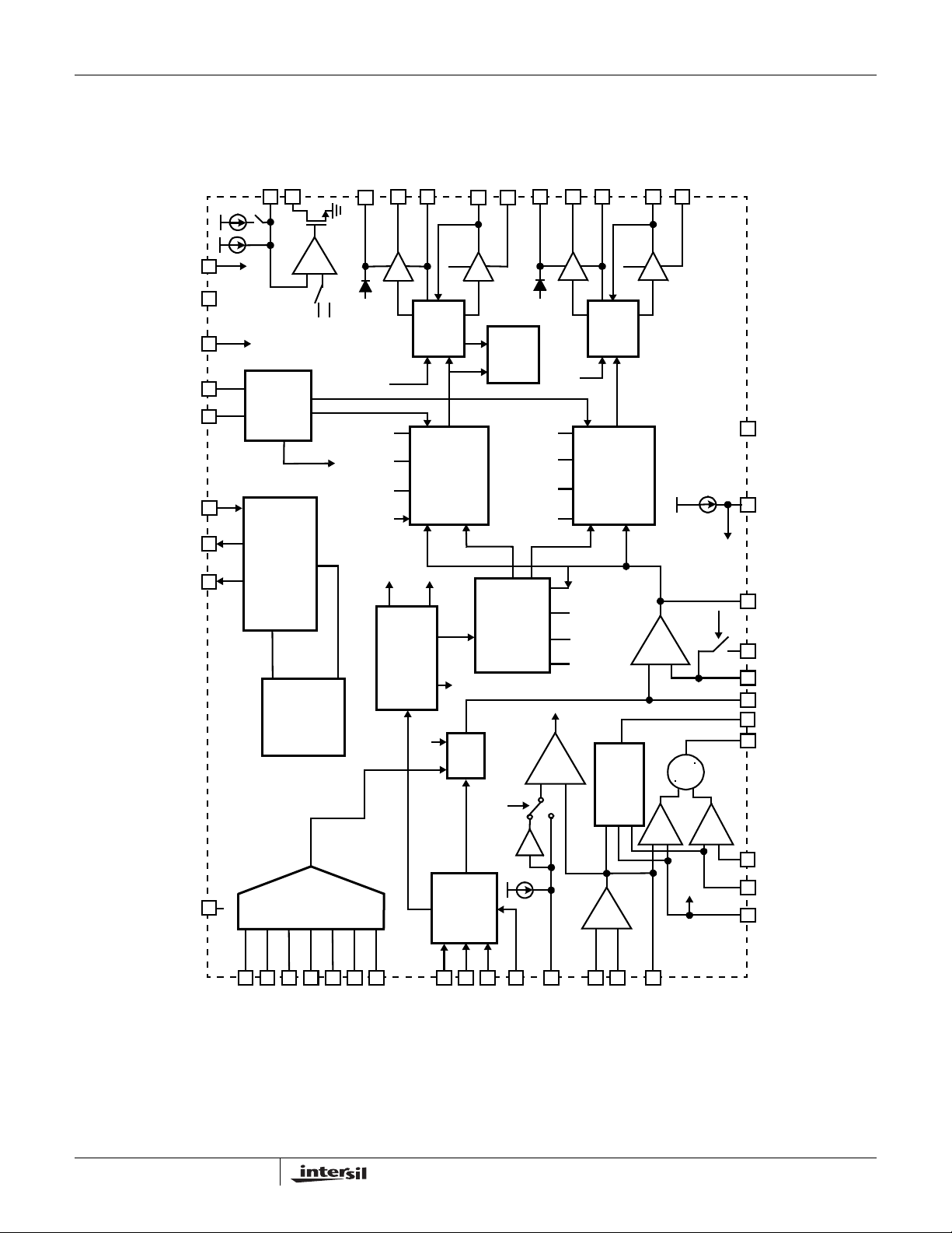
Functional Block Diagram
ISL6262A
PVCC
VDD
VIN
ISEN2
ISEN1
3V3
PGOOD
CLK_EN#
RBIAS
6µA
54µA
PVCC
VIN
NTC
VR_TT#
1.2V
CURRENT
BALANCE
PGOOD
MONITOR
AND LOGIC
P
FLT
FAULT AND
PGOOD
LOGIC
DAC
-
I_BALF
GOOD
DACOUT
+
1.24V
BOOT1
PVCC
VSOFT
VIN
OC
CH1
CH1 CH2
CONTROL
UGATE1
DRIVER
LOGIC
FLT
MODULATOR
PHASE
LOGIC
VO
REQUEST
MODE CHANGE
PHASE1
PVCC
SINGLE
PHASE
SOFT
MODE
CONTROL
LGATE1
PGND1
PVCC
ULTRA-
SONIC
TIMER
VSOFT
CH2
PHASE
SEQUENCER
SINGLE
PHASE
0.66
10µA
BOOT2
VIN
OC
-
UGATE2
DRIVER
FLT
MODULATOR
Vw
VO
VIN
OC
+
DROOP
PHASE2
PVCC
LOGIC
-
+
VSOFT
MULTIPLIER
LGATE2
E/A
+
-
1
-
+
PGND2
SINGLE
PHASE
+
VO
GND
VW
Vw
COMP
FB2
FB
SOFT
PMON
VDIFF
+
1
-
+
RTN
VSEN
VO
VID0
VID1
VID2
VID3
VID4
VID5
VID6
PSI#
VR_ON
DPRSLPVR
OCSET
DPRSTP#
DFB
VSUM
FIGURE 1. SIMPLIFIED FUNCTIONAL BLOCK DIAGRAM OF ISL6262A
8
DROOP
FN6343.1
December 23, 2008
Page 9
V
(V)
ISL6262A
Typical Performance Curves 300kHz Operation, 2xIRF7821 as Upper Devices and 2xIRF7832 as Bottom Devices
100
VIN = 8.0V
90
80
70
60
50
40
EFFICIENCY (%)
30
20
10
0
0 5 10 15 20 25 30 35 40 45 50
VIN = 12.6V
V
= 19.0V
IN
I
OUT
(A)
FIGURE 2. ACTIVE MODE EFFICIENCY , 2 PHASE, CCM,
PSI# = HIGH, VID = 1.15V
100
VIN = 8.0V
90
80
70
60
50
40
EFFICIENCY (%)
30
20
10
0
02468101214161820
VIN = 12.6V
VIN = 19.0V
I
OUT
(A)
FIGURE 4. ACTIVE MODE EFFICIENCY , 1 PHASE, CCM,
PSI# = LOW, VID = 1.15V
1.16
VIN = 8.0V
VIN = 12.6V
= 19.0V
V
IN
01020304050
I
(A)
OUT
(V)
OUT
V
1.14
1.12
1.10
1.08
1.06
1.04
1.02
FIGURE 3. ACTIVE MODE LOAD LINE, 2 PHASE, CCM,
PSI# = HIGH, VID = 1.15V
1.16
1.15
1.14
(V)
1.13
OUT
V
1.12
1.11
1.10
0 4 6 8 10 20
2 12141618
VIN = 12.6V
VIN = 19.0V
I
OUT
VIN = 8.0V
(A)
FIGURE 5. ACTIVE MODE LOAD LINE, 1 PHASE, CCM,
PSI# = LOW, VID = 1.15V
100
90
80
70
EFFICIENCY (%)
60
50
0.1 1.0 10
FIGURE 6. DEEPER SLEEP MODE EFFICIENCY FIGURE 7. DEEPER SLEEP MODE LOAD LINE
VIN = 8.0V
VIN = 19.0V
VIN = 12.6V
I
(A)
OUT
9
0.765
0.760
0.755
0.750
OUT
0.745
0.740
0.735
0246810
I
OUT
(A)
VIN = 8.0V
VIN = 12.6V
VIN = 19.0V
FN6343.1
December 23, 2008
Page 10

ISL6262A
Typical Performance Curves 0.36µH Filter Inductor and 4 x 330µF Output SP Caps and 24 x 22µF Ceramic Caps
V
C
OUT
SOFT
= 15nF
VR_ON
V
SOFT
VR_ON
V
SOFT
C
SOFT
V
OUT
= 15nF
FIGURE 8. SOFT-ST ART WA VEFORM SHOWING SLEW RA TE
OF 2.5mV/µs AT VID = 1V, I
LOAD
= 10A
V
@ 1.4375V
OUT
V
@ 1.2V
OUT
PGD_IN
IMVP-6+_PWRGD
CLK_EN#
FIGURE 10. SOFT-ST ART W AVEFORM SHOWING CLK_EN#
AND IMVP-6+ PGOOD
FIGURE 9. SOFT-ST ART WA VEFORM SHOWING SLEW RA TE
OF 2.5mV/µs AT VID = 1.4375V, I
LOAD
= 10A
FIGURE 11. 2 PHASE CURRENT BALANCE, FULL LOAD (50A)
LINE TRANSIENT
V
OUT
IIN
V
IN
FIGURE 12. 8V-20V INPUT LINE TRANSIENT RESPONSE,
C
= 240µF
IN
10
V
OUT
IIN
FIGURE 13. INRUSH CURRENT AT START -UP, V
VID = 1.4375V, I
LOAD
= 10A
IL1, IL2
= 8V ,
IN
FN6343.1
December 23, 2008
Page 11

ISL6262A
Typical Performance Curves 0.36µH Filter Inductor and 4 x 330µF Output SP Caps and 24 x 22µF Ceramic Caps (Continued)
V
OUT
LOAD TRANSIENT
FIGURE 14. LOAD STEP-UP RESPONSE AT THE CPU
SOCKET MPGA479, 35A LOAD STEP @ 200A/µs,
2 PHASE CCM
V
OUT
VID3
V
OUT
DYNAMIC VID
ACTIVE MODE
PHASE1,
PHASE2
FIGURE 15. VID3 CHANGE OF 010X000 FROM 1V TO 1.1V
WITH DPRSLPVR = 0, DPRSTP# = 1, PSI# = 1
VID3
V
OUT
LOAD TRANSIENT
FIGURE 16. LOAD DUMP RESPONSE AT THE CPU SOCKET
MPGA479, 35A LOAD STEP @ 200A/µs, 2 PHASE
CCM
PSI#
V
CORE
PHASE1
DROP PHASE IN
ACTIVE MODE
PHASE2
DYNAMIC VID
ACTIVE MODE
PHASE1,
PHASE2
FIGURE 17. VID3 CHANGE OF 010X000 FROM 1.1V TO 1V
WITH DPRSLPVR = 0, DPRSTP# = 1, PSI# = 1
PSI#
V
CORE
PHASE2
PHASE1
ADD PHASE IN
ACTIVE MODE
FIGURE 18. 2-CCM TO 1-CCM UPON PSI# ASSERTION WITH
VID LSB CHANGE, AT DPRSLPVR = 0,
DPRSTP# = 1, I
LOAD
= 10A
11
FIGURE 19. 1-CCM TO 2-CCM UPON PSI# DEASSERTION
WITH VID LSB CHANGE AT DPRSLPVR = 0,
DPRSTP# = 1
FN6343.1
December 23, 2008
Page 12

ISL6262A
Typical Performance Curves 0.36µH Filter Inductor and 4 x 330µF Output SP Caps and 24 x 22µF Ceramic Caps (Continued)
DPRSLPVR
V
OUT
PHASE1
PHASE2
C4 ENTRY WITH
PSI# ASSERTION
FIGURE 20. C4 ENTRY WITH VID CHANGE 0011X00 FROM
1.2V TO 1.15V, I
2-CCM TO 1-DCM, PSI# TOGGLE FROM 1 TO 0
= 2A, TRANSITION OF
LOAD
WITH DPRSLPVR FROM 0 TO 1
DPRSTP#
DPRSTP#
DPRSLPVR
DPRSLPVR
VID6
VID6
DPRSLPVR
C4 EXIT/PHASE ADD
V
OUT
PHASE1
PHASE2
FIGURE 21. VID3 CHANGE OF 010X000 FROM 1V TO 1.1V
WITH DPRSLPVR = 0, DPRSTP# = 1, PSI# = 1
DPRSLPVR
V
OUT
C4 ENTRY WITH PSI# = 0
V
CORE
Vcore
FIGURE 22. SLOW C4 EXIT WITH DELAY OF DPRSLPVR,
FROM VID1000000 (0.7V) TO 0110000 (0.9V)
V
OUT
PGOOD
IL1, IL2
FIGURE 24. OVERCURRENT PROTECTION FIGURE 25. 1.7V OVERVOLTAGE PROTECTION SHOWS
PHASE1
PHASE2
FIGURE 23. C4 ENTRY WITH VID CHANGE OF 011X011 FROM
0.8625V TO 0.7625V, I
1-DCM
PGOOD
= 3A, 1-CCM TO
LOAD
PHASE1
V
OUT
OUTPUT VOLTAGE PULLED LOW TO 0.9V AND
PWM THREE-STATE
12
FN6343.1
December 23, 2008
Page 13

ISL6262A
Typical Performance Curves 0.36µH Filter Inductor and 4 x 330µF Output SP Caps and 24 x 22µF Ceramic Caps (Continued)
V
Vcore
V
CORE
Vcore
CORE
PMON AFTER 40kHz FILTER
PMON after 40 kHz filter
FIGURE 26. VID TRANSITION FROM 1V TO 1.15V I
EXTERNAL FILTER 40kΩ AND 100pF AT PMON
V
Vcore
CORE
PMON
PMON
PMON
PMON
LOAD
=21A,
PMON
PMON
PMON AFTER 40kHZ FILTER
PMON after 40 kHz filter
FIGURE 27. VID = 1.15V, LOAD TRANSIENT OF 0A T O 36A
WITH INTEL® VTT TOOL, 1kHz REPETITION
RATE, 50% DUTY CYCLE, TR = 56
V
CORE
Vcore
PMON
PMON
PMON AFTER 40kHZ FILTER
PMON after 40 kHz filter
PMON AFTER 40kHZ FILTER
PMON after 40 kHz filter
FIGURE 28. VID = 1.15V, LOAD RELEASE FROM 36A TO 0A
WITH INTEL® VTT TOOL, 1kHz REPETITION
RATE, 50% DUTY CYCLE, TR = 56
1.8
1.6
19V, 1.15V, 40A
1.4
1.2
19V, 1.15V, 30A
1.0
0.8
PMON (V)
19V, 1.15V, 20A
0.6
0.4
19V, 1.15V, 10A
0.2
19V, 1.15V, 5A
0.0
0.0 1.0 2.0 3.0 4.0 5.0 6.0 7.0
CURRENT SOURCING (mA)
7Ω
FIGURE 30. POWER MONITOR CURRENT SOURCING
CAPABILITY
13
FIGURE 29. VID = 1.15V, LOAD APPLICATION FROM
0A TO 36A WITH INTEL® VTT TOOL, 1kHz
REPETITION RATE, 50% DUTY CYCLE, TR = 56
0.8
0.7
0.6
0.5
0.4
PMON (V)
0.3
0.2
0.1
0.00
0.0 0.5 1.0 1.5 2.0 2.5 3.0 3.5 4.0 4.5
VID = 1.15V, I
VID = 1.15V, I
VID = 1.15V, I
OUT
CURRENT SINKING (mA)
= 15A
OUT
= 10A
VID = 1.15V, I
OUT
180Ω
= 2.5A
OUT
= 5A
FIGURE 31. POWER MONITOR CURRENT SINKING
CAPABILITY
December 23, 2008
FN6343.1
Page 14

ISL6262A
Simplified Application Circuit for DCR Current Sensing
V
+5
V
VIN
UGATE1
BOOT1
PHASE1
LGATE1
PGND1
ISEN1
UGATE2
BOOT2
PHASE2
LGATE2
PGND2
ISEN2
VSUM
OCSET
VO
IN
R
6
C
6
C
5
R
N
NTC
NETWORK
VSUM
VR_TT#
VID<0:6>
DPRSTP#
DPRSLPVR
PSI#
CLK_ENABLE#
VR_ON
IMVP-6+_PWRGD
REMOTE
SENSE
V
+3.3
R
12
3V3
VDD
PVCC
RBIAS
R
NTC
13
VR_TT#
C
8
SOFT
ISL6262A
VIDs
DPRSTP#
DPRSLPVR
PSI#
PMON
CLK_EN#
VR_ON
PGOOD
VSEN
R
2
R
C
3
3
R
C
R
1
1
RTN
VDIFF
7
FB2
FB
COMP
C
2
R
FSET
VW
C
GND
9
R
DROOPDFB
R
5
C
4
4
V
IN
C
7
L
O
R
10
C
R
ISEN1
R
8
VSUM
V
IN
C
8
R
ISEN2
R
9
L
L
VO'
V
O
C
O
L
O
R
11
C
L
L
VO'
VSUM
C
CS
VO'
FIGURE 32. ISL6262A BASED TWO-PHASE BUCK CONVERTER WITH INDUCTOR DCR CURRENT SENSING
14
FN6343.1
December 23, 2008
Page 15

ISL6262A
Simplified Application Circuit for Resistive Current Sensing
V
+5
V
VIN
UGATE1
BOOT1
PHASE1
LGATE1
PGND1
ISEN1
UGATE2
BOOT2
PHASE2
LGATE2
PGND2
ISEN2
VSUM
OCSET
VO
IN
V
IN
C
C
6
V
IN
C
C
5
VSUM
C
R
6
HF
VR_TT#
VID<0:6>
DPRSTP#
DPRSLPVR
PSI#
CLK_ENABLE#
VR_ON
IMVP-6+_PWRGD
REMOTE
SENSE
V
+3.3
R
11
3V3
VDD
PVCC
RBIAS
R
NTC
12
VR_TT#
C
9
SOFT
ISL6262A
VIDs
DPRSTP#
DPRSLPVR
PSI#
PMON
CLK_EN#
VR_ON
PGOOD
VSEN
R
2
R
C
3
3
R
C
R
1
1
RTN
VDIFF
7
FB2
FB
COMP
C
2
R
FSET
VW
C
GND
9
R
DROOPDFB
R
5
C
4
4
7
L
R
8
8
L
R
9
R
ISEN1
VSUM
L
R
L
ISEN2
R
S
R
10
C
L
VO'
V
O
C
O
R
S
R
11
C
L
VO'
VSUM
VO'
FIGURE 33. ISL6262A BASED TWO-PHASE BUCK CONVERTER WITH RESISTIVE CURRENT SENSING
15
FN6343.1
December 23, 2008
Page 16

ISL6262A
Theory of Operation
The ISL6262A is a two-phase regulator implementing Intel
IMVP-6+ protocol and includes embedded gate drivers for
reduced system cost and board area. The regulator provides
optimum steady-state and transient performance for
microprocessor core applications up to 50A. System
efficiency is enhanced by idling one phase at low-current
and implementing automatic DCM-mode operation.
The heart of the ISL6262A is R
Robust Ripple Regulator modul a to r. The R
combines the best features of fixed frequency PWM and
hysteretic PWM while eliminating many of their
shortcomings. The ISL6262A modulator internally
synthesizes an analog of the inductor ripple current and
uses hysteretic comparators on those signals to establish
PWM pulse widths. Operating on these large-amplitude,
noise-free synthesized signals allows the ISL6262A to
achieve lower output ripple and lower phase jitter than either
conventional hysteretic or fixed frequency PWM controllers.
Unlike conventional hysteretic converters, the ISL6262A has
an error amplifier that allows the controller to maintain a
0.5% voltage regulation accuracy throughout the VID range
from 0.75V to 1.5V.
The hysteresis window voltage is relative to the error
amplifier output such that load current transients results in
increased switching frequency, which gives the R
a faster response than conventional fixed frequency PWM
controllers. Transient load current is inherently shared
between active phases due to the use of a common
hysteretic window voltage. Individual average phase
voltages are monitored and controlled to equally share the
static current among the active phases.
Start-Up Timing
With the controller's +5V VDD voltage above the POR
threshold, the start-up sequence begins when VR_ON
exceeds the 3.3V logic HIGH threshold. Approximately
100µs later, SOFT and VOUT begin ramping to the boot
voltage of 1.2V. At start-up, the regulator always operates in
a 2-phase CCM mode, regardless of control signal assertion
levels. During this internal, the SOFT cap is charged by
41µA current source. If the SOFT capacitor is selected to be
20nF, the SOFT ramp will be at 2mV/µs for a soft-start time
of 600µs. Once VOUT is within 10% of the boot voltage for
13 PWM cycles (43µs for frequency = 300kHz), then
CLK_EN# is pulled LOW and the SOFT cap is
charged/discharged by approximately 200µA. Therefore,
VOUT slews at +10mV/µs to the voltage set by the VID pins.
Approximately 7ms later, PGOOD is asserted HIGH. Typical
start-up timing is shown in Figure 34.
3
Technology™, Intersil’s
3
modulator
3
regulator
V
DD
VR_ON
100µs
SOFT AND VO
CLK_EN#
IMVP-6+ PGOOD
FIGURE 34. SOFT-START WA V EFORMS US ING A 20nF SO FT
CAPACITOR
10mV/µs
2mV/µs
VBOOT
90%
13 SWITCHING CYCLES
-7ms
VID COMMANDED
VOLTAGE
Static Operation
After the start sequence, the output voltage will be regulated
to the value set by the VID inputs shown in Table 1. The
entire VID table is presented in the IntelIMVP-6+
specification. The ISL6262A will control the no-load output
voltage to an accuracy of ±0.5% over the range of 0.75V to
1.5V.
TABLE 1. TRUNCA TED VID TABLE FOR INTEL® IMVP-6+
SPECIFICATION
VID6 VID5 VID4 VID3 VID2 VID1 VID0 VOUT (V)
00000001.5000
00000011.4875
00001011.4375
00100011.2875
00111001.15
01101010.8375
01110110.7625
11000000.3000
11111110.0000
A fully-differential amplifier implements core voltage sensing
for precise voltage control at the microprocessor die. The
inputs to the amplifier are the VSEN and RTN pins.
As the load current increases from zero, the output voltage
will droop from the VID table value by an amount
proportional to current to achieve the IMVP-6+ load line. The
ISL6262A provides for current to be measured using either
resistors in series with the channel inductors as shown in the
application circuit of Figure 33, or using the intrinsic series
resistance of the inductors as shown in the application circuit
of Figure 32. In both cases, signals representing the inductor
currents are summed at VSUM, which is the non-inverting
input to the DROOP amplifier shown in the “Functional Block
Diagram” on page 8 of Figure 1. The voltage at the DROOP
pin minus the output voltage, VO´, is a high-bandwidth
16
FN6343.1
December 23, 2008
Page 17

ISL6262A
analog of the total inductor current. This voltage is used as
an input to a differential amplifier to achieve the IMVP-6+
load line, and also as the input to the overcurrent protection
circuit.
When using inductor DCR current sensing, a single NTC
element is used to compensate the positive temperature
coefficient of the copper winding thus maintaining the
load-line accuracy.
In addition to monitoring the total current (used for DROOP
and overcurrent protection), the individual channel average
currents are also monitored and used for balancing the load
between channels. The IBAL circuit will adjust the channel
pulse-widths up or down relative to the other channel to
cause the voltages presented at the ISEN pins to be equal.
The ISL6262A controller can be configured for two-channel
operation, with the channels operating 180° apart. The
channel PWM frequency is determined by the value of
R
connected to pin VW as shown in Figure 32 and
FSET
Figure 33. Input and output ripple frequencies will be the
channel PWM frequency multiplied by the number of active
channels.
High Efficiency Operation Mode
The ISL6262A has several operating modes to optimize
efficiency. The controller's operational modes are designed
to work in conjunction with the Intel® IMVP-6+ control
signals to maintain the optimal system configuration for all
IMVP-6+ conditions. These operating modes are established
by the IMVP-6+ control signal inputs such as PSI#,
DPRSLPVR, and DPRSTP# as shown in Table 2. At high
current levels, the system will operate with both phases fully
active, responding rapidly to transients and deliver the
maximum power to the load. At reduced load-current levels,
one of the phases may be idled. This configuration will
minimize switching losses, while still maintaining transient
response capability. At the lowest current levels, the
controller automatically configures the system to operate in
single-phase automatic-DCM mode, thus achieving the
highest possible efficiency. In this mode of operation, the
lower MOSFET will be configured to automatically detect
and prevent discharge current flowing from the output
capacitor through the inductors, and the switching frequency
will be proportionately reduced, thus greatly reducing both
conduction and switching losses. If ISEN2 is pulled to 5V, the
ISL6262A operates at 1-phase-only mode. The ISL6262A
always enables the diode emulation mode of phase 1 in
always-1-phase configuration.
Smooth mode transitions are facilitated by the R
3
Technology™, which correctly maintains the internally
synthesized ripple currents throughout mode transitions. The
controller is thus able to deliver the appropriate current to the
load throughout mode transitions. The controller contains
embedded mode-transition algorithms that maintain
voltage-regulation for all control signal input sequences and
durations.
Mode-transition sequences often occur in concert with VID
changes; therefore the timing of the mode transitions of
ISL6262A has been carefully designed to work in concert
with VID changes. For example, transitions into single-phase
will be delayed until the VID induced voltage ramp is
complete. This allows the associated output capacitor
charging current to be shared by both inductor paths. While
in single-phase automatic-DCM mode, VID changes will
initiate an immediate return to two-phase CCM mode. This
ensures that both inductor paths share the output capacitor
charging current and are fully active for the subsequent load
current increases.
The controller contains internal counters that prevent
spurious control signal glitches from resulting in unwanted
mode transitions. Control signals of less than two switching
periods do not result in phase-idling. Signals of less than
seven switching periods do not result in implementation of
automatic-DCM mode.
While transitioning to single-phase operation, the controller
smoothly transitions current from the idling-phase to the
active-phase, and detects the idling-phase zero-current
condition. During transitions into automatic-DCM or
forced-CCM mode, the timing is carefully adjusted to
eliminate output voltage excursions. When a phase is
added, the current balance between phases is quickly
restored.
TABLE 2. CONTROL SIGNAL TRUTH TABLES FOR OPERATION MODES OF ISL6262A IN TWO-PHASE DESIGN
Intel IMVP-6+
COMPLIANT LOGIC
OTHER LOGIC
COMMANDS
DPRSLPVR DPRSTP# PSI# PHASE OPERATION MODES EXPECTED CPU MODE
0 1 1 2-phase CCM Active mode
0 1 0 1-phase CCM Active mode
1 0 1 1-phase diode emulation Deeper sleep mode
1 0 0 1-phase diode emulation Deeper sleep mode
0 0 1 2-phase CCM
0 0 0 1-phase CCM
1 1 1 2-phase CCM
1 1 0 1-phase CCM
17
FN6343.1
December 23, 2008
Page 18

ISL6262A
While PSI# is high, both phases are switching. If PSI# is
asserted low and either DPRSTP# or DPRSLPVR are not
asserted, the controller will transition to CCM operation with
only phase 1 switching, and both MOSFETs of phase 2 will
be off. The controller will thus eliminate switching losses
associated with the unneeded channel.
V
AND V
OUT
FIGURE 35. DEEPER SLEEP TRANSITION SHOWING
SOFT
-2.5mV/µs
2.5mV/µs
DPRSLPVR
VID #
DPRSLPVR'S EFFECT ON EXIT SLEW RATE
10mV/µs
When PSI#, DPRSTP#, and DPRSLPVR are all asserted,
the controller will transition to single-phase DCM mode. In
this mode, both MOSFETs associated with phase 2 are off,
and the ISL6262A turns off the lower MOSFET of Channel 1
whenever the Channel 1 current decays to zero. As load is
further reduced, the phase 1 channel switching frequency
decreases to maintain high efficiency.
Dynamic Operation
See Figure 35. The ISL6262A responds to changes in VID
command voltage by slewing to new voltages with a dV/dt
set by the SOFT capacitor and by the state of DPRSLPVR.
With C
voltage will move at ±2.8mV/s for large changes in voltage.
= 15nF and DPRSLPVR HIGH, the output
SOFT
For DPRSLPVR LOW, the large signal dV/dt will be
±10mV/s. As the output voltage approaches the VID
command value, the dV/dt moderates to prevent overshoot.
Keeping DPRSLPVR HIGH for voltage transitions into and
out of Deeper Sleep will result in low dV/dt output voltage
changes with resulting minimized audio noise. For fastest
recovery from Deeper Sleep to Active mode, holding
DPRSLPVR LOW results in maximum dV/dt. Therefore, the
ISL6262A is IMVP-6+ compliant for DPRSTP# and
DPRSLPVR logic.
Intersil's R
3
Technology™ has intrinsic voltage feedforward.
As a result, high-speed input voltage steps do not result in
significant output voltage perturbations. In response to load
current step increases, the ISL6262A will transiently raise
the switching frequency so that response time is decreased
and current is shared by two channels.
Protection
The ISL6262A provides overcurrent, overvoltage, undervoltage protection and over-temperature protection as
shown in Table 3.
Overcurrent protection is tied to the voltage droop which is
determined by the resistors selected as described in
“Component Selection and Application” on page 19“. After
the load-line is set, the OCSET resistor can be selected to
detect overcurrent at any level of droop voltage. An
overcurrent fault will occur when the load current exceeds
the overcurrent setpoint voltage while the regulator is in a
2-phase mode. While the regulator is in a 1-phase mode of
operation, the overcurrent setpoint is automatically reduced
to 66% of two-phase overcurrent level. For overcurrents less
than 2.5 times the OCSET level, the over-load condition
must exist for 120µs in order to trip the OC fault latch. This is
shown in Figure 24.
TABLE 3. FAULT-PROTECTION SUMMARY OF ISL6262A
FAULT DURATION PRIOR
TO PROTECTION PROTECTION ACTIONS FAULT RESET
Overcurrent fault 120µs PWM1, PWM2 three-state,
PGOOD latched low
Way-Overcurrent fault <2µs PWM1, PWM2 three-state,
PGOOD latched low
Overvoltage fault (1.7V) Immediately Low-side MOSFET on until Vcore
<0.85V, then PWM three-state,
PGOOD latched low (OV to 1.7V
always)
Overvoltage fault (+200mV) 1ms PWM1, PWM2 three-state,
PGOOD latched low
Undervoltage fault
(-300mV)
Unbalance fault
(7.5mV)
Over-temperature
fault (NTC <1.18V)
1ms PWM1, PWM2 three-state,
PGOOD latched low
1ms PWM1, PWM2 three-state,
PGOOD latched low
Immediately VR_TT# goes low N/A
18
VR_ON toggle or VDD toggle
VR_ON toggle or VDD toggle
VDD toggle
VR_ON toggle or VDD toggle
VR_ON toggle or VDD toggle
VR_ON toggle or VDD toggle
December 23, 2008
FN6343.1
Page 19

ISL6262A
For overloads exceeding 2.5xthe set level, the PWM outputs
will immediately shut off and PGOOD goes low to maximize
protection due to hard shorts.
In addition, excessive phase unbalance (for example, due to
gate driver failure) will be detected in two-phase operation
and the controller will be shutdown after one millisecond's
detection of the excessive phase current unbalance. The
phase unbalance is detected by the voltage on the ISEN
pins if the difference is greater than 9mV.
Undervoltage protection is independent of the overcurrent
limit. If the output voltage is less than the VID set value by
300mV or more, a fault will latch after one millisecond in that
condition. The PWM outputs will turn off and PGOOD will go
low. Note that most practical core regulators will have the
overcurrent set to trip before the -300mV undervoltage limit.
There are two levels of overvoltage protection and response.
1. For output voltage exceeding the set value by +200mV
for one millisecond, a fault is declared. All of the above
faults have the same action taken: PGOOD is latched low
and the upper and lower power MOSFETs are turned off
so that inductor current will decay through the MOSFET
body diodes. This condition can be reset by bringing
VR_ON low or by bringing VDD below 4V. When these
inputs are returned to their high operating levels, a
soft-start will occur.
2. The second level of overvoltage protection beha ves
differently (see Figure 25). If the output exceeds 1.7V, an
OV fault is immediately declared, PGOOD is latched low
and the low-side MOSFETs are turned on. The low-side
MOSFET s will remain on until the output voltage is pulled
down below about 0.85V, at which time all MOSFETs are
turned off. If the output again rises above 1.7V, the
protection process is repeated. This offers the maximum
amount of protection against a shorted high-side
MOSFET while preventing output ringing below ground.
The 1.7V OV is not reset with VR_ON, but requires that
VDD be lowered to reset. The 1.7V OV de tector is acti ve
at all times that the controller is enabled including after
one of the other faults occurs so that the processor is
protected against high-side MOSFET leakage while the
MOSFETs are commanded off.
The ISL6262A has a thermal throttling feature. If the voltage
on the NTC pin goes below the 1.2V over-temperature
threshold, the VR_TT# pin is pulled low indicating the need
for thermal throttling to the system oversight processor. No
other action is taken within the ISL6262A in response to
NTC pin voltage.
given by: V
pmon=VCCSENSE
*(V
droop-VO
) * 17.5. In
always-single-phase design, the output voltage PMON pin is
given by: V
pmon=VCCSENSE
*(V
droop-VO
) * 35.
The power consumed by the CPU can be calculated by:
P
cpu=Vpmon
/ (17.5 * 0.0021) (Watt), where 0.0021 is the
typical load line slope. The power monitor load regulation is
approximately 7Ω. Within its sourcing/sinking current
capability range, when the power monitor loading changes to
1mA, the output of the power monitor will change to 7mV.
The 7Ω impedance is associated with the layout and
package resistance of PMON inside the IC. In practical
applications, compared to the load resistance on the PMON
pin, 7Ω output impedance contributes no significant error.
Component Selection and Application
Soft-Start and Mode Change Slew Rates
The ISL6262A uses two slew rates for various modes of
operation. The first is a slow slew rate used to reduce in-rush
current during start-up. It is also used to reduce audible
noise when entering or exiting Deeper Sleep Mode. A faster
slew rate is used to exit out of Deeper Sleep and to enhance
system performance by achieving active mode regulation
more quickly. Note that the SOFT cap current is bidirectional.
The current is flowing into the SOFT capacitor when the
output voltage is commanded to rise and out of the SOFT
capacitor when the output voltage is commanded to fall.
The two slew rates are determined by commanding one of
two current sources onto the SOFT pin. As can be seen in
Figure 36, the SOFT pin has a capacitance to ground. Also,
the SOFT pin is the input to the error amplifier and is,
therefore, the commanded system voltage. Depending on
the state of the system (that is, Start- Up or Active mode) and
the state of the DPRSLPVR pin, one of the two currents
shown in Figure 36 will be used to charge or discharge this
capacitor, thereby controlling the slew rate of the
commanded voltage. These currents can be found under
“SOFT-START CURRENT” on page 4 of the Electrical
Specifications table.
ISL6262A
I
SS
I
2
ERROR
AMPLIFIER
+
Power Monitor
The power monitor signal is an analog output. Its magnitude
is proportional to the product of V
difference between V
droop
CCSENSE
and VO, which is the
programmed voltage droop value, equal to load current
multiplied by the load line impedance (for example 2.1mΩ).
The output voltage of the PMON pin in two-phase design is
19
and the voltage
SOFT
+
V
C
SOFT
FIGURE 36. SOFT PIN CURRENT SOURCES FOR FAST AND
SLOW SLEW RATES
REF
FN6343.1
December 23, 2008
Page 20

ISL6262A
The first current, labeled ISS, is given in the Table Electrical
Specifications on page 3 as 42µA. This current is used
during soft-start. The second current, I
the larger of the two currents, labeled I
sums with ISS to get
2
in the
GV
Table Electrical Specifications on page 3 . This total current
is typically 205µA with a minimum of 180µA.
The IMVP-6+ specification reveals the critical timing
associated with regulating the output voltage. The symbol,
SLEWRATE, as given in the IMVP-6+ specification will
determine the choice of the SOFT capacitor, C
SOFT
, by
Equation 1.
C
SOFT
GV
------------------------------------
=
SLEWRATE
(EQ. 1)
I
Using a SLEWRATE of 10mV/µs and the typical IGV value
given in the Electrical Specification table of 205µA, C
SOFT
is
as shown in Equation 2.
C
SOFT
205μ A10mV1μs⁄()⁄=
(EQ. 2)
A choice of 0.015µF would guarantee a SLEWRATE of
10mV/µs is met for the minimum I
Electrical Specification table. This choice of C
value given in the
GV
SOFT
will then
control the Start-Up slewrate as well. One should expect the
output voltage to slew to the Boot value of 1.2V at a rate
given by Equation 3.
dV
-------
dt
I
SS
-------------------
C
SOFT
41μ A
---------------------- -
0.015μ F
2.8mV μs⁄== =
(EQ. 3)
Selecting RBIAS
To properly bias the ISL6262A, a reference current is
established by placing a 147kΩ, 1% tolerance resistor from
the RBIAS pin to ground. This will provide a highly accurate
10µA current source from which the OCSET reference
current can be derived.
Care should be taken in layout that the resistor is placed
very close to the RBIAS pin and that a good quality signal
ground is connected to the opposite side of the RBIAS
resistor. Do not connect any other components to this pin as
this would negatively impact performance. Capacitance on
this pin would create instabilities and should be avoided.
noise immunity, the 3.3V supply should be decoupled to
digital ground rather than to analog ground.
As mentioned in “Theory of Operation” on page 16,
CLK_EN# is logic level high at start-up until approximately
43µs after the V
Approximately 43µs after V
-core is in regulation at the Boot level.
CC
-core are within regulation,
CC
CLK_EN# goes low, triggering an internal timer for the
IMVP6_PWRGD signal. This timer allows IMVP-6_PWRGD
to go high approximately 6.8ms after CLK_EN# goes low.
Static Mode of Operation - Processor Die Sensing
Die sensing is the ability of the controller to regulate the core
output voltage at a remotely sensed point. This allows the
voltage regulator to compensate for various resistive drops
in the power path and ensure that the voltage seen at the
CPU die is the correct level independent of load current.
The VSEN and RTN pins of the ISL6262A are connected to
Kelvin sense leads at the die of the processor through the
processor socket. These signal names are Vcc_sense and
Vss_sense respectively. This allows the voltage regulator to
tightly control the processor voltage at the die, independent
of layout inconsistencies and voltage drops. This Kelvin
sense technique provides for extremely tight load line
regulation.
These traces should be laid out as noise sensitive traces. For
optimum load line regulation performance, the traces
connecting these two pins to the Kelvin sense leads of the
processor must be laid out away from rapidly rising voltage
nodes, (switching nodes) and other noisy traces. To achieve
optimum performance, place common mode and differential
mode filters to analog ground on VSEN and RTN as shown in
Figure 37.
Intersil recommends the use of the R
connected to V
and ground as shown in Figure 37.
OUT
These resistors provide voltage feedback in the event that
the system is powered up without a processor installed.
These resistors typically range from 20 to 100Ω.
opn1
and R
opn2
Start-Up Operation - CLK_EN# and PGOOD
The ISL6262A provides a 3.3V logic output pin for
CLK_EN#. The 3V3 pin allows for a system 3.3V source to
be connected to separated circuitry inside the ISL6262A,
solely devoted to the CLK_EN# function. The output is a
3.3V CMOS signal with 4mA sourcing and sinking capability.
This implementation removes the need for an external
pull-up resistor on this pin, and due to the normal level of this
signal being a low, removes the leakage path from the 3.3V
supply to ground through the pull-up resistor. This reduces
the 3.3V supply current that would occur under normal
operation with a pull-up resistor and prolongs battery life. For
20
FN6343.1
December 23, 2008
Page 21

ISEN1 ISEN2
ISL6262A
+
0.01µF
ISEN2
10µA
+
+
R
1
1
RTN
OPN2
VO'
R
drp2
R
OCSET
R
drp1
TO V
VO'
R
SERIES
Cn
R
NTC
OUT
TO PROCESSOR
SOCKET KELVIN
CONNECTIONS
OCSET
VSUM
+
DROOP
+
-
+
VSEN
330pF
330pF
DFB
-
DROOP
R
VCC_SENSE
VSS_SENSE
opn1
ISEN1
OC
INTERNAL TO
ISL6262A
VDIFF
FIGURE 37. SIMPLIFIED SCHEMATIC FOR DROOP AND DIE SENSING WITH INDUCTOR DCR CURRENT SENSING
Setting the Switching Frequency - FSET
The R3 modulator scheme is not a fixed frequency PWM
architecture. The switching frequency can increase during
the application of a load to improve transient performance.
It also varies slightly due to changes in input and output
voltage and output current, but this variation is normally less
than 10% in continuous conduction mode.
The resistor connected between the VW and COMP pins of
the ISL6262A adjusts the switching window, and therefore
adjusts the switching frequency (Figure 32). The R
FSET
resistor that sets up the switching frequency of the converter
operating in CCM can be determined using Equation 4,
where R
R
FSET
For 300kHz operation, R
is in kΩ and the switching period is in µs.
FSET
kΩ() period μs()0.29–()2.33•=
is suggested to be 6.81kΩ. In
fset
(EQ. 4)
discontinuous conduction mode (DCM), the ISL6262A runs in
period stretching mode. The switching frequency is dependent
on the load current level. In general, the lighter load, the slower
switching frequency. Therefore, the switching loss is much
reduced for the light load operation, which is important for
conserving the battery power in the portable application.
Voltage Regulator Thermal Throttling
lntel® IMVP-6+ technology supports thermal throttling of the
processor to prevent catastrophic thermal damage to the
voltage regulator. The ISL6262A features a thermal monitor
that senses the voltage change across an externally placed
negative temperature coefficient (NTC) thermistor.
VSUM
R
I
PAR
VO'
VSUM
VSUM
PHASE1
R
I
PHASE2
RS
L
S
R
L1
ISEN1
L
2
R
L2
ISEN2
1
VO'
+ -
C
Vdcr
C
L2
+ -
L1
2
VO'
Vdcr
DCR
DCR
1
R
O1
R
O2
Proper selection and placement of the NTC thermistor
allows for detection of a designated temperature rise by the
system.
Figure 38 shows the thermal throttling feature with
hysteresis. At low temperature, SW1 is on and SW2
connects to the 1.2V side. The total current going into NTC
pin is 60µA. The voltage on the NTC pin is higher than the
threshold voltage of 1.2V and the comparator output is low.
VR_TT# is pulling up high by the external resistor.
54µA
NTC
+
V
R
NTC
NTC
-
1.24V
R
s
FIGURE 38. CIRCUITRY ASSOCIATED WITH THE THERMAL
THROTTLING FEATURE IN ISL6262A
6µA
SW1
-
+
SW2
1.20V
INTERNAL TO
ISL6262A
When the temperature increases, the NTC resistor value on
the NTC pin decreases. Thus, the voltage on the NTC pin
decreases to a level lower than 1.2V. The comp arator output
changes polarity and turns SW1 off and connects SW2 to
1.24V. This pulls VR_TT# low and sends the signal to start
thermal throttle. There is a 6µA current reduction on the NTC
V
OUT
C
BULK
ESR
VR_TT#
21
FN6343.1
December 23, 2008
Page 22

ISL6262A
pin and 20mV voltage increase on the threshold voltage of
the comparator in this state. The VR_TT# signal will be used
to change the CPU operation and decrease the power
consumption. When the temperature goes down, the NTC
thermistor voltage will eventually go up. When the NTC pin
voltage increases to 1.24V, the comparator output will then
be able to flip back. Such a temperature hysteresis feature of
VR_TT# is illustrated in Figure 39. T
represents the higher
1
temperature point at which the VR_TT# goes from low to
high due to the system temperature rise. T
represents the
2
lower temperature point at which the VR_TT# goes high
from low because the system temperature decreases to the
normal level.
VR_TT#
LOGIC_1
LOGIC_0
FIGURE 39. TEMPERATURE HYSTERESIS OF VR_TT#
T1
T
2
T (°C)
Usually, the NTC thermistor's resistance can be
approximated by Equation 5.
R
NTC
T() R
NTCTo
1
⎛⎞
------------------- -
b
•
⎝⎠
T 273+
e•=
-----------------------
–
To 273+
1
(EQ. 5)
T is the temperature of the NTC thermistor and b is a
parameter constant depending on the thermistor material.
T
is the reference temperature in which the approximation
o
is derived. The most common temperature for T
is +25°C.
o
For example, there are commercial NTC thermistor products
with b = 2750k, b = 2600k, b = 4500k or b = 4250k.
From the operation principle of the VR_TT# circuit
explained, the NTC resistor satisfies Equation 6 and 8.
R
NTCT1
R
NTCT2
()RS+
()RS+
-------------- -
60μ A
1.24V
--------------- -
54μ A
20kΩ==
22.96kΩ==
(EQ. 6)
(EQ. 7)
1.2V
From Equation 6 and Equation 7, Equation 8 can be derived,
R
NTCT2
()R
()– 2.96kΩ=
NTCT1
(EQ. 8)
Using Equation 5 into Equation 8, the required nominal NTC
resistor value can be obtained by: Equation 9.
1
⎛⎞
-----------------------
b
•
⎝⎠
To273+
•
e–
1
⎛⎞
-----------------------
b
•
⎝⎠
T1273+
(EQ. 9)
R
NTCTo
2.96kΩ e
----------------------------------------------------------------------------- -
=
e
1
⎛⎞
-----------------------
b
•
⎝⎠
T2273+
For those cases where the constant b is not accurate
enough to approximate the resistor value, the manufacturer
provides the resistor ratio information at different
temperatures. The nominal NTC resistor value may be
expressed in another way shown in Equation 10.
Λ
R
NTC
2.96kΩ
–
()ΛR
T
2
NTC
(EQ. 10)
T1()
NTCTo
=
Λ
R
NTC T()
R
where is the normalized NTC resistance to its
----------------------------------------------------------------------- -
nominal value. Most data sheets of the NTC thermistor give
the normalized resistor value based on its value at +25°C.
Once the NTC thermistor resistor is determined, the series
resistor can be derived by: Equation 11.
1.2V
-------------- -
R
S
60μA
Once R
at T
NTCTo
and the actual T2 temperature can be found in:
2
R
NTC
T1()20kΩ R
–=–=
NTC_T
1
(EQ. 11)
and Rs is designed, the actual NTC resistance
Equations 12, and 13.
R
NTC_T
T
2_actual
2.96kΩ R
+=
R
NTC_T
-------------------------
R
NTCTo
NTC_T
1
2
1
1 273 To+()⁄+ln
2
-----------------------------------------------------------------------------------
⎛⎞
1
-- -
⎜⎟
b
⎝⎠
(EQ. 12)
273–=
(EQ. 13)
For example, if using Equations 9, 10 and 11 to design a
thermal throttling circuit with the temperature hysteresis
+100°C to +105°C, since T
= +105°C and T2= +100°C,
1
and if we use a Panasonic NTC with b = 4700, Equation 9
gives the required NTC nominal resistance as
R
NTC_To
=459kΩ.
In fact, the data sheet gives the resistor ratio value at
+100°C to +105°C, which is 0.03956 and 0.03322
respectively. The b value 4700k in the Panasonic data sheet
only covers to +85°C. Therefore, using Equation 10 is more
accurate for +100°C design, the required NTC nominal
resistance at +25°C is 467kΩ. The closest NTC resistor
value from the manufacturer is 467kΩ. So the series
resistance is given by Equation 14.
R
S
20kΩ R
NTC_105°C
20kΩ 15.65kΩ 4.35kΩ=–=–=
(EQ. 14)
The closest standard resistor is 4.42kΩ. Furthermore, the NTC
resistance at T
R
NTC_T2
is given by Equation 15.
2
2.96kΩ R
+ 18.16kΩ==
NTC_T1
(EQ. 15)
Therefore, the NTC branch is designed to have a 470k NTC
and 4.42k resistor in series. The part number of the NTC
thermistor is ERTJ0EV474J. It is a 0402 package. The NTC
22
FN6343.1
December 23, 2008
Page 23

ISL6262A
10µA
OC
+
INTERNAL TO
ISL6262A
+
1
+
+
VDIFF VSEN
-
+
1
-
RTN
FIGURE 40. EQUIVALENT MODEL FOR DROOP AND DIE SENSING USING DCR SENSING
DROOP
-
OCSET
VSUM
+
DFB
DROOP
Rdrp2
VO'
thermistor should be placed in the spot which gives the best
indication of the temperature of voltage regulator circuit.
Static Mode of Operation - S tatic Droop Using DCR
Sensing
As previously mentioned, the ISL6262A has an internal
differential amplifier which provides for very accurate voltage
regulation at the die of the processor. The load line
regulation is also accurate for both two-phase and
single-phase operation. The process of selecting the
components for the appropriate load line droop is explained
here.
For DCR sensing, the process of compensation for DCR
resistance variation to achieve the desired load line droop
has several steps and is somewhat iterative.
The two-phase solution using DCR sensing is shown in
Figure 37. There are two resistors connecting to the terminals
of inductor of each phase. These are labeled R
These resistors are used to obtain the DC voltage drop across
each inductor. Each inductor will have a certain level of DC
current flowing through it, and this current, when multiplied by
the DCR of the inductor, creates a small DC voltage drop
across the inductor terminal. When this voltage is summed with
the other channels DC voltages, the total DC load current can
be derived.
R
is typically 1Ω to 10Ω. This resistor is used to tie the
O
outputs of all channels together and thus create a summed
average of the local CORE voltage output. R
through an understanding of both the DC and transient load
currents. This value will be covered in the next section.
However, it is import a nt to keep in mind that the outp ut of
each of these R
resistors are tied together to create the
S
VSUM voltage node. With both the outpu ts o f R
together, the si mplified mode l for the droop circuit can be
derived. This is presented in Figure 40.
and RO.
S
is determined
S
and RS tied
O
RS
EQV
Vdcr
RO
--------
=
2
EQVIOUT
RO
---------
=
EQV
2
×=
DCR
-------------
2
RS
VSUM
+
Cn
VN
-
Rdrp1
VO'
Rntc Rseries+()Rpar×
-----------------------------------------------------------------------
Rn
=
Rntc Rseries+()Rpar+
Figure 40 shows the simplified model of the droop circuitry.
Essentially one resistor can replace the R
phase and one R
resistor can replace the RS resistors of
S
resistors of each
O
each phase. The total DCR drop due to load current can be
replaced by a DC source, the value of which is given by:
Equation 16.
V
DCR_EQU
OUT
---------------------------------
=
2
(EQ. 16)
I
DCR•
For the convenience of analysis, the NTC network
comprised of R
labeled as a single resistor R
ntc
, R
series
and R
par
in Figure 40.
n
, given in Figure 37, is
The first step in droop load line compensation is to adjust
R
, RO
n
EQV
and RS
such that sufficient droop voltage
EQV
exists even at light loads between the VSUM and VO' nodes.
As a rule of thumb, we start with the voltage drop across the
R
network, VN, to be 0.5 to 0.8 times V
n
DCR_EQU
. This ratio
provides for a fairly reasonable amount of light load signal
from which to arrive at droop.
The resultant NTC network resistor value is dependent on
the temperature and given by Equation 17.
+()R
R
seriesRntc
--------------------------------------------------------------
T()
=
R
n
R
seriesRntcRpar
For simplicity, the gain of Vn to the V
•
++
par
dcr_equ
(EQ. 17)
is defined by
G1, also dependent on the temperature of the NTC
thermistor.
Δ
R
T()
n
-------------------------------------------
T()
G
=
1
DCR T() DCR
R
n
T() RS
+
25° C
EQV
1 0.00393*(T-25)+()•=
(EQ. 18)
(EQ. 19)
Therefore, the output of the droop amplifier divided by the
total load current can be expressed as shown in
Equation 20, where R
is the realized load line slope
droop
and 0.00393 is the temperature coefficient of the copper.
23
FN6343.1
December 23, 2008
Page 24

)
)
ISL6262A
R
droopG1
T()
DCR
-------------------
2
25
1 0.00393*(T-25)+()k
•••=
droopamp
(EQ. 20)
To achieve the droop value independent from the
temperature of the inductor, it is equivalently expressed by
Equation 21.
G1T() 1 0.00393*(T-25)+()G
≅•
1t etarg
(EQ. 21)
The non-inverting droop amplifier circuit has the gain
K
droopamp
k
droopamp
G
1target
expressed as:
R
drp2
--------------- -
1
+=
R
drp1
is the desired gain of Vn over I
OUT
• DCR/2.
Therefore, the temperature characteristics of gain of Vn is
described by Equation 22.
G
1t etarg
G1T()
For the G
R
R
R
RS
-------------------------------------------------------
=
1 0.00393*(T-25)+()
= 0.76:
1target
= 10kΩ with b = 4300,
ntc
= 2.61kΩ, and
series
= 11kΩ
par
= 1825Ω generates a desired G1, close to the
EQV
(EQ. 22
feature specified in Equation 22.
The actual G1 at +25°C is 0.769. For different G1 and NTC
thermistor preferences, the design file to generate the proper
value of R
ntc
, R
series
, R
, and RS
par
is provided by
EQV
Intersil.
Then, the individual resistors from each phase to the VSUM
node, labeled R
and RS2 in Figure 37, are then given by
S1
Equation 23.
R
2RS
•=
S
So, R
and R
EQV
= 3650Ω. Once we know the attenuation of the RS
s
network, we can then determine the droop amplifier
N
(EQ. 23)
gain required to achieve the load line. Setting
R
= 1k_1%, then R
drp1
•
2R
Rdrp2
⎛⎞
-----------------------------------------------
⎝⎠
DCR G1 25°C()•
droop
Droop Impedance (R
can be found using Equation 24.
drp2
•=
1–
R
drp1
) = 0.0021 (V/A) as per the Intel
droop
(EQ. 24
IMVP-6+ specification, DCR = 0.0008Ω typical for a 0.36µH
inductor, R
R
is then given by Equation 25.
drp2
Rdrp2
= 1kΩ and the attenuation gain (G1) = 0.77,
drp1
•
2R
droop
⎛⎞
---------------------------------------
⎝⎠
0.0008 0.769•
1–
1kΩ 5.82kΩ≈•=
(EQ. 25)
PCB traces sensing the inductor voltage should be going
directly to the inductor pads.
Once the board has been laid out, some adjustments may
be required to adjust the full load droop voltage. This is fairly
easy and can be accomplished by allowing the system to
achieve thermal equilibrium at full load, and then adjusting
R
to obtain the appropriate load line slope.
drp2
To see whether the NTC has compensated the temperature
change of the DCR, the user can apply full load current and
wait for the thermal steady state and see how much the
output voltage will deviate from the initial voltage reading. A
good compensation can limit the drift to 2mV. If the output
voltage is decreasing with temperature increase, that ratio
between the NTC thermistor value and the rest of the
resistor divider network has to be increased. The user
should follow the evaluation board value and layout of NTC
as much as possible to minimize engineering time.
The 2.1mV/A load line should be adjuste d by R
drp2
based
on maximum current, (not based on small current steps like
10A), as the droop gain might vary between each 10A step.
Basically, if the max current is 40A, the required droop
voltage is 84mV. The user shou ld have 40A load current on
and look for 84mV droop. If the drop voltage is less than
84mV, for example 80mV, the new value will be calculated
by: using Equation 26.
84mV
Rdrp2_new
----------------
80mV
Rdrp1 Rdrp2+()Rdrp1–=
(EQ. 26)
For the best accuracy , th e effective resistance on the DFB
and VSUM pins should be identical so that the bias current
of the droop amplifier does not cause an offset voltage. In
the previous example, the resistance on the DFB pin is
R
in parallel with R
drp1
or 853Ω. The resistance on the VSUM pin is R
with RS
or 5.87k in parallel with 1.825k or 1392Ω. The
EQV
, that is, 1k in parallel with 5.82k
drp2
in parallel
n
mismatch in the effective resistances is 1404 - 53 = 551Ω.
Do not let the mismatch get larger than 600Ω. To reduce the
mismatch, multiply both R
drp1
and R
by the appropriate
drp2
factor. The appropriate factor in the example is
1404/853 = 1.65. In summary, the predicted load line with
the designed droop network parameters based on the
Intersil design tool is shown in Figure 41
Note, we choose to ignore the RO resistors because they do
not add significant error.
These designed values in R
network are very sensitive to
n
the layout and coupling factor of the NTC to the inductor. As
only one NTC is required in this application, this NTC should
be placed as close to the Channel 1 inductor as possible and
24
FN6343.1
December 23, 2008
Page 25

ISL6262A
.
2.25
2.2
2.15
2.1
LOAD LINE (mV/A)
2.05
0 20406080100
INDUCTOR TEMPERATURE (°C)
FIGURE 41. LOAD LINE PERFORMANCE WITH NTC
THERMAL COMPENSATION
Dynamic Mode of Operation - Dynamic Droop
Using DCR Sensing
Droop is very important for load transient performance. If the
system is not compensated correctly, the output voltage
could sag excessively upon load application and potentially
create a system failure. The output voltage could also take a
long period of time to settle to its final value. This could be
problematic if a load dump were to occur during this time.
This situation would cause the output voltage to rise above
the no load setpoint of the converter and could potentially
damage the CPU.
The L/DCR time constant of the inductor must be matched to
the R
L
-------------
DCR
Solving for C
n
Note, R
constant matches the C
previously, the transient performance will be optimum. As in
the static droop case, this process may require a slight
adjustment to correct for layout inconsistencies. For the
example of L = 0.36µH with 0.8mΩ DCR, Cn is calculated in
Equation 29.
n
The value of this capacitor is selected to be 330nF. As the
inductors tend to have 20% to 30% tolerances, this cap
generally will be tuned on the board by examining the
transient voltage. If the output voltage transient has an initial
dip, lower than the voltage required by the load line, and
slowly increases back to the steady state, the capacitor is
too small and vice versa. It is better to have the capacitor
value a little bigger to cover the tolerance of the inductor to
time constant as shown in Equation 27.
n*Cn
R
•
nRSEQV
----------------------------------
RS
+
R
n
n
L
-------------
DCR
---------------------------------- -
=
•
R
nRSEQV
----------------------------------
RS
+
R
n
was neglected. As long as the inductor time
O
--------------------------------------------------------------------- -
parallel 5.823K, 1.825K()
•=
C
n
EQV
we now have Equation 28.
EQV
, Rn and Rs time constants as given
n
0.36μ H
--------------------
0.0008
330nF≈=
(EQ. 27)
(EQ. 28)C
(EQ. 29)C
prevent the output voltage from going lower than the
specification. This cap needs to be a high grade capacitor
like X7R with low tolerance. There is another consideration
in order to achieve better time constant match mentioned
previously. The NPO/COG (class-I) capacitors have only 5%
tolerance and a very good thermal characteristics. But those
capacitors are only available in small capacitance values. In
order to use such capacitors, the resistors and thermistors
surrounding the droop voltage sensing and droop amplifier
has to be resized up to 10X to reduce the capacitance by
10X. But attention has to be paid in balancing the impedance
of droop amplifier in this case.
Dynamic Mode of Operation - Compensation
Parameters
Considering the voltage regulator as a black box with a
voltage source controlled by VID and a series impedance, in
order to achieve the 2.1mV/A load line, the impedance
needs to be 2.1mΩ. The compensation design has to target
the output impedance of the converter to be 2.1mΩ. There is
a mathematical calculation file available to the user. The
power stage parameters such as L and Cs are needed as
the input to calculate the compensation component values.
Attention has to be paid to the input resistor to the FB pin.
T oo high of a resistor will cause an error to the output voltage
regulation because of bias current flowing in the FB pin. It is
better to keep this resistor below 3k when using this file.
Static Mode of Operation - Current Balance Using
DCR or Discrete Resistor Current Sensing
Current Balance is achieved in the ISL6262A through the
matching of the voltages present on the ISEN pins. The
ISL6262A adjusts the duty cycles of each phase to maintain
equal potentials on the ISEN pins. R
inductor, or around each discrete current resistor, are used
to create a rather large time constant such that the ISEN
voltages have minimal ripple voltage and represent the DC
current flowing through each channel's inductor. For
optimum performance, R
is chosen to be 10kΩ and CL is
L
selected to be 0.22µF . When discrete resistor sensing is
used, a capacitor most likely needs to be placed in parallel
with R
to properly compensate the current bal a nce circuit.
L
ISL6262A uses RC filter to sense the average voltage on
phase node and forces the average voltage on the phase
node to be equal for current balance. Even though the
ISL6262A forces the ISEN voltages to be almost equal, the
inductor currents will not be exactly equal. Using DCR
current sensing as an example, two errors have to be added
to find the total current imbalance.
1. Mismatch of DCR: If the DCR has a 5% tolerance then
the resistors could mismatch by 10% worst case. If each
phase is carrying 20A then the phase currents mismatch
by 20A*10% = 2A.
2. Mismatch of phase voltages/offset voltage of ISEN pins:
The phase voltages are within 2mV of each other by
and CL around each
L
25
FN6343.1
December 23, 2008
Page 26

ISL6262A
current balance circuit. The error current that results is
given by 2mV/DCR. If DCR = 1mΩ then the error is 2A.
In the previous example, the two errors add to 4A. For the
two phase DC/DC, the currents would be 22A in one phase
and 18A in the other phase. In the above analysis, the
current balance can be calculated with 2A/20A = 10%. This
is the worst case calculation. For example, the actual
tolerance of two 10% DCRs is 10%*sqrt(2) = 7%.
There are provisions to correct the current imbalance due to
layout or to purposely divert current to certain phase for
better thermal management. Customer can put a resistor in
parallel with the current sensing capacitor on the phase of
interest in order to purposely increase the current in that
phase.
If the PC board trace resistance from the inductor to the
microprocessor are significantly different between two
phases, the current will not be balanced perfectly. Intersil
has a proprietary method to achieve the perfect current
sharing in case of severe unbalanced layout.
When choosing the current sense resistor, both the
tolerance of the resistance and the TCR are important. Also,
the current sense resistor’s combined tolerance at a wide
temperature range should be calculated.
Droop Using Discrete Resistor Sensing - Static/
Dynamic Mode of Operation
Figure 42 shows the equivalent circuit of a discrete current
sense approach. Figure 33 shows a more detailed
schematic of this approach. Droop is solved the same way
as the DCR sensing approach with a few slight
modifications.
Solving for the R
Intel IMVP-6+ specification, R
R
=1kΩ, we obtain in Equation 32.
drp1
drp2
K
droopamp
drp2
value, R
1–()R
• 3.2kΩ==
drp1
= 0.0021(V/A) as per the
droop
= 0.001Ω and
sense
(EQ. 32)R
These values are extremely sensitive to layout. Once the
board has been laid out, some tweaking may be required to
adjust the full load droop. This is fairly easy and can be
accomplished by allowing the system to achieve thermal
equilibrium at full load, and then adjusting R
to obtain the
drp2
desired droop value.
Fault Protection - Overcurrent Fault Setting
As previously described, the overcurrent protection of the
ISL6262A is related to the droop voltage. Previously we
have calculated that the droop voltage = ILoad*R
where R
is the load line slope specified as 0.0021 (V/A)
droop
in the Intel IMVP-6+ specification. Knowing this relationship,
the overcurrent protection threshold can be set up as a
voltage droop level. Knowing this voltage droop level, one
can program in the appropriate drop across the R
resistor. This voltage drop will be referred to as Voc. Once
the droop voltage is greater than Voc, the PWM drives will
turn off and PGOOD will go low.
The selection of R
desire an overcurrent trip level, I
is given in Equation 33. Assuming we
OC
, of 55A, and knowing
OC
from the Intel Specification that the load line slope, R
0.0021 (V/A), we can then calculate for R
as shown in
OC
Equation 33.
IOCR
OC
•
droop
-----------------------------------
10μ A
55 0.0021•
------------------------------
10 10
•
11.5kΩ===
6–
droop
OC
,
droop
(EQ. 33)R
is
First, because there is no NTC required for thermal
compensation, the R
resistor network in the previous
n
section is not required. Second, because there is no time
constant matching required, the C
component is not
n
matched to the L/DCR time constant. This component does
indeed provide noise immunity and therefore is populated
with a 39pF capacitor.
The R
values in the previous section, RS = 1.5k_1%, are
S
sufficient for this approach.
Now the input to the droop amplifier is essentially the
Vrsense voltage. This voltage is given by Equation 30.
R
sense
------------------- -
•=
EQV
I
OUT
2
The gain of the droop amplifier, K
for the ratio of the R
to droop impedance, R
sense
droopamp
, must be adjusted
droop
(EQ. 30)Vrsense
. We
use the Equation 31.
R
droop
K
droopamp
------------------- -
R
sense
2•=
(EQ. 31)
Note: If the droop load line slope is not -0.0021 (V/A) in the
application, the overcurrent setpoint will differ from
predicted.
26
FN6343.1
December 23, 2008
Page 27

OC
INTERNAL TO
ISL6262A
10µA
+
+
1
-
+
+
+
1
-
DROOP
OCSET
+
-
DROOP
VSUM
DFB
+Voc -Roc
VSUM
Rdrp2
Cn
RS
RS
+
VN
-
Vrsense
--------
=
EQV
EQVIOUT
2
Rsense
-----------------------
×=
2
VDIFF VSEN
RTN
VO'
Rdrp1
VO'
RO
EQV
RO
---------
=
2
FIGURE 42. EQUIVALENT MODEL FOR DROOP AND DIE SENSING USING DISCRETE RESISTOR SENSING
All Intersil U.S. products are manufactured, assembled and tested utilizing ISO9000 quality systems.
Intersil Corporation’s quality certifications can be viewed at www.intersil.com/design/quality
Intersil products are sold by description only. Intersil Corporation reserves the right to make changes in circuit design, software and/or specifications at any time without
notice. Accordingly, the reader is cautioned to verify that data sheets are current before placing orders. Information furnished by Intersil is believed to be accurate and
reliable. However, no responsibility is assumed by Intersil or its subsidiaries for its use; nor for any infringements of patents or other rights of third parties which may result
from its use. No license is granted by implicat ion or oth erwise u nde r any p a tent or p at ent r ights of Intersil or its subsidiari es.
For information regarding Intersil Corporation and its products, see www.intersil.com
27
FN6343.1
December 23, 2008
Page 28

Package Outline Drawing
L48.7x7
48 LEAD QUAD FLAT NO-LEAD PLASTIC PACKAGE
Rev 4, 10/06
7.00
6
PIN 1
INDEX AREA
ISL6262A
A
B
36
37
4X
44X
5.5
0.50
48
6
PIN #1 INDEX AREA
1
(4X) 0.15
( 6 . 80 TYP )
( 4 . 30 )
TOP VIEW
TYPICAL RECOMMENDED LAND PATTERN
7.00
0 . 90 ± 0 . 1
( 44X 0 . 5 )
( 48X 0 . 23 )
( 48X 0 . 60 )
25
24
48X 0 . 40± 0 . 1
BOTTOM VIEW
SIDE VIEW
0 . 2 REF
C
DETAIL "X"
0 . 00 MIN.
0 . 05 MAX.
12
13
4
BASE PLANE
5
4. 30 ± 0 . 15
M0.10 C AB
0.23 +0.07 / -0.05
SEE DETAIL "X"
C
C
0.10
SEATING PLANE
C0.08
28
NOTES:
Dimensions are in millimeters.1.
Dimensions in ( ) for Reference Only.
2.
Dimensioning and tolerancing conform to AMSE Y14.5m-1994.
3.
Unless otherwise specified, tolerance : Decimal ± 0.05
4.
Dimension b applies to the metallized terminal and is measured
between 0.15mm and 0.30mm from the terminal tip.
Tiebar shown (if present) is a non-functional feature.
5.
The configuration of the pin #1 identifier is optional, but must be
6.
located within the zone indicated. The pin #1 identifier may be
either a mold or mark feature.
FN6343.1
December 23, 2008
 Loading...