

®
ISL6237
Data Sheet March 18, 2008
High-Efficiency, Quad-Output, Main Power
Supply Controllers for Notebook
Computers
The ISL6237 dual step-down, switch-mode power-supply
(SMPS) controller generates logic-supply voltages in
battery-powered systems. The ISL6237 includes two
pulse-width modulation (PWM) controllers, 5V/3.3V and
1.5V/1.05V. The output of SMPS1 can also be adjusted from
0.7V to 5.5V . The SMPS2 o utput can be adjusted from 0.5V to
2.5V by setting REFIN2 voltage. This device features a linear
regulator providing 3.3V/5V, or adjustable from 0.7V to 4.5V
output via LDOREFIN. The linear regulator provides up to
100mA output current with automatic linear-regulator
bootstrapping to the BYP input. When in switchover, the LDO
output can source up to 200mA. The ISL6237 includes
on-board power-up sequencing, power-good (POK_) output s,
digital soft-start, and internal so f t-stop output di scharge that
prevents negative voltages on shutdown .
Constant on-time PWM control scheme operates without
sense resistors and provides 100ns response to load
transients while maintaining a relatively constant switching
frequency . The unique ul trasonic pul se-ski pping mode
maintains the switching frequency above 25kHz, which
eliminates noise in audio applications. Other features include
pulse skipping, which maximizes efficiency in light-load
applications, and fixed-frequency PWM mode, which reduces
RF interference in sensitive applications.
Ordering Information
PART
NUMBER
(Note)
ISL6237IRZ ISL6237 IRZ -40 to +100 32 Ld 5x5 QFN L32.5x5B
ISL6237IRZ-T* ISL6237 IRZ -40 to +100 32 Ld 5x5 QFN
*Please refer to TB347 for details on reel specifications.
NOTE: These Intersil Pb-free plastic packaged products employ
special Pb-free material sets; molding compounds/die attach materials
and 100% matte tin plate PLUS ANNEAL - e3 termination finish, which
is RoHS compliant and compatible with both SnPb and Pb-free
soldering operations. Intersil Pb-free products are MSL classified at
Pb-free peak reflow temperatures that meet or exceed the Pb-free
requirements of IPC/JEDEC J STD-020.
PART
MARKING
TEMP.
RANGE
(°C)
PACKAGE
(Pb-free)
Tape and Reel
PKG.
DWG. #
L32.5x5B
FN6418.4
Features
• Wide Input Voltage Range 5.5V to 25V
• Dual Fixed 1.05V/3.3V and 1.5V/5.0V Outputs or
Adjustable 0.7V to 5.5V (SMPS1) and 0.5V to 2.5V
(SMPS2), ±1.5% Accuracy
• 1.7ms Digital Soft-Start and Independent Shutdown
• Fixed 3.3V/5.0V, or Adjustable Output 0.7V to 4.5V,
±1.5% (LDO): 200mA
• 2.0V Reference Voltage
• Constant ON-TIME Control with 100ns Load-Step
Response
• Selectable Switching Frequency
•r
Current Sensing
DS(ON)
• Programmable Current Limit with Foldback Capability
• Selectable PWM, Skip or Ultrasonic Mode
• BOOT Voltage Monitor with Automatic Refresh
• Independent POK1 and POK2 Comparators
• Soft-Start with Pre-Biased Output and Soft-Stop
• Independent ENABLE
• High Efficiency - Up to 97%
• Very High Light Load Efficiency (Skip Mode)
• 5mW Quiescent Power Dissipation
• Thermal Shutdown
• Extremely Low Components Count
• Pb-Free (RoHS Compliant)
Applications
• Notebook and Sub-Notebook Computers
• PDAs and Mobile Communication Devices
• 3-Cell and 4-Cell Li+ Battery-Powered Devices
• DDR1, DDR2, and DDR3 Power Supplies
• Graphic Cards
• Game Consoles
• Telecommunication
1
CAUTION: These devices are sensitive to electrostatic discharge; follow proper IC Handling Procedures.
1-888-INTERSIL or 1-888-468-3774
| Intersil (and design) is a registered trademark of Intersil Americas Inc.
Copyright Intersil Americas Inc. 2007, 2008. All Rights Reserved
All other trademarks mentioned are the property of their respective owners.
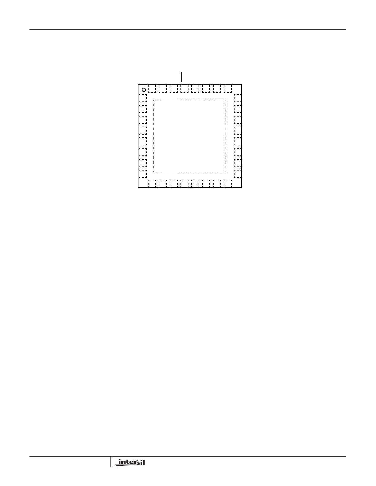
Pinout
REF
ISL6237
ISL6237
(32 LD 5x5 QFN)
TOP VIEW
REFIN2
ILIM2
OUT2
SKIP
POK2
32 31 30 29 28 27 26 25
1
EN2
UGATE2
PHASE2
24
BOOT2
TON
VCC
EN_LDO
NC
VIN
LDO
LDOREFIN
2
3
4
5
6
7
8
9 10111213141516
BYP
FB1
OUT1
ILIM1
POK1
EN1
LGATE2
23
PGND
22
GND
21
NC
20
PVCC
19
LGATE1
18
BOOT1
17
UGATE1
PHASE1
2
FN6418.4
March 18, 2008
ISL6237
Absolute Voltage Ratings
VIN, EN_LDO to GND . . . . . . . . . . . . . . . . . . . . . . . . .-0.3V to +27V
BOOT_ to GND . . . . . . . . . . . . . . . . . . . . . . . . . . . . . .-0.3V to +33V
BOOT_ to PHASE_ . . . . . . . . . . . . . . . . . . . . . . . . . . . .-0.3V to +6V
VCC, EN_, SKIP
PVCC, POK_ to GND . . . . . . . . . . . . . . . . . . . . . . . . . .-0.3V to +6V
LDO, FB1, REFIN2, LDOREFIN to GND . . . -0.3V to (VCC + 0.3V)
OUT_, REF to GND . . . . . . . . . . . . . . . . . . . .-0.3V to (VCC + 0.3V
, TON,
Thermal Information
Thermal Resistance (Typical) θJA (°C/W) θJC (°CW)
32 Ld QFN (Notes 1, 2) . . . . . . . . . . . . 32 3.0
Operating Temperature Range . . . . . . . . . . . . . . . .-40°C to +100°C
Junction Temperature . . . . . . . . . . . . . . . . . . . . . . . . . . . . . .+150°C
Storage Temperature Range . . . . . . . . . . . . . . . . . .-65°C to +150°C
Pb-free reflow profile . . . . . . . . . . . . . . . . . . . . . . . . . .see link below
http://www.intersil.com/pbfree/Pb-FreeReflow.asp
UGATE_ to PHASE_ . . . . . . . . . . . . . . . . . . -0.3V to (PVCC + 0.3V)
ILIM_ to GND. . . . . . . . . . . . . . . . . . . . . . . . . -0.3V to (VCC + 0.3V)
LGATE_, BYP to GND. . . . . . . . . . . . . . . . . -0.3V to (PVCC + 0.3V)
PGND to GND . . . . . . . . . . . . . . . . . . . . . . . . . . . . . .-0.3V to + 0.3V
LDO, REF Short Circuit to GND . . . . . . . . . . . . . . . . . . .Continuous
VCC Short Circuit to GND . . . . . . . . . . . . . . . . . . . . . . . . . . . . . . . 1s
LDO Current (Internal Regulator) Continuous . . . . . . . . . . . . 100mA
LDO Current (Switched Over to OUT1) Continuous . . . . . . +200mA
CAUTION: Do not operate at or near the maximum ratings listed for extended periods of time. Exposure to such conditions may adversely impact product reliability and
result in failures not covered by warranty.
NOTES:
is measured in free air with the component mounted on a high effective thermal conductivity test board with “direct attach” features. See
1. θ
JA
Tech Brief TB379.
2. For θ
, the “case temp” location is the center of the exposed metal pad on the package underside.
JC
3. Limits established by characterization and are not production tested.
4. Parts are 100% tested at +25°C. Temperature limits established by characterization and are not production tested.
Electrical Specifications No load on LDO, OUT1, OUT2, and REF, V
V
EN_LDO
PARAMETER CONDITIONS
=5V, TA= -40°C to +100°C, unless otherwise noted. Typical values are at TA = +25°C.
= 12V, EN2 = EN1 = VCC, VBYP = 5V, PVCC = 5V,
IN
MIN
(Note 4) TYP
MAX
(Note 4) UNITS
MAIN SMPS CONTROLLERS
VIN Input Voltage Range LDO in regulation 5.5 25 V
= LDO, V
V
IN
< 4.43V 4.5 5.5 V
OUT1
3.3V Output Voltage in Fixed Mode VIN = 5.5V to 25V, REFIN2 > (VCC - 1V), SKIP = 5V 3.285 3.330 3.375 V
1.05V Output Voltage in Fixed Mode V
1.5V Output Voltage in Fixed Mode V
5V Output Voltage in Fixed Mode V
FB1 in Output Adjustable Mode V
= 5.5V to 25V, 3.0 < REFIN2 < (VCC - 1.1V),
IN
SKIP
=5V
= 5.5V to 25V, FB1 = VCC, SKIP = 5V 1.482 1.500 1.518 V
IN
= 5.5V to 25V, FB1 = GND, SKIP = 5V 4.975 5.050 5.125 V
IN
= 5.5V to 25V 0.693 0.700 0.707 V
IN
1.038 1.05 1.062 V
REFIN2 in Output Adjustable Mode VIN = 5.5V to 25V 0.7 2.50 V
SMPS1 Output Voltage Adjust Range SMPS1 0.70 5.50 V
SMPS2 Output Voltage Adjust Range SMPS2 0.50 2.50 V
SMPS2 Output Voltage Accuracy
REFIN2 = 0.7V to 2.5V, SKIP
=VCC -1.0 1.0 %
(Referred for REFIN2)
DC Load Regulation Either SMPS, SKIP
Either SMPS, SKIP
Either SMPS, SKIP
Line Regulation Either SMPS, 6V < V
= VCC, 0 to 5A -0.1 %
= REF, 0 to 5A -1.7 %
= GND, 0 to 5A -1.5 %
< 24V 0.005 %/V
IN
Current-Limit Current Source Temperature = +25°C 4.75 5 5.25 µA
ILIM_ Adjustment Range 0.2 2 V
Current-Limit Threshold (Positive, Default) ILIM_ = VCC, GND - PHASE_
93 100 107 mV
(No temperature compensation)
3
FN6418.4
March 18, 2008
ISL6237
Electrical Specifications No load on LDO, OUT1, OUT2, and REF, V
PARAMETER CONDITIONS
Current-Limit Threshold
(Positive, Adjustable)
V
EN_LDO
=5V, TA= -40°C to +100°C, unless otherwise noted. Typical values are at TA = +25°C. (Continued)
GND - PHASE_ V
= 12V, EN2 = EN1 = VCC, VBYP = 5V, PVCC = 5V,
IN
MIN
(Note 4) TYP
= 0.5V 40 50 60 mV
ILIM_
V
= 1V 93 100 107 mV
ILIM_
V
= 2V 185 200 215 mV
ILIM_
MAX
(Note 4) UNITS
Zero-Current Threshold SKIP = GND, REF, or OPEN, GND - PHASE_ 3 mV
Current-Limit Threshold (Negative, Default) SKIP
= VCC, GND - PHASE_ -120 mV
Soft-Start Ramp Time Zero to full limit 1.7 ms
Operating Frequency (V
= GND), SKIP = VCC SMPS 1 400 kHz
tON
SMPS 2 500 kHz
(V
= REF or OPEN),
tON
SKIP
= VCC
= VCC), SKIP = VCC SMPS 1 200 kHz
(V
tON
SMPS 1 400 kHz
SMPS 2 300 kHz
SMPS 2 300 kHz
On-Time Pulse Width V
Minimum Off-Time T
= GND (400kHz/500kHz) V
tON
V
= REF or OPEN
tON
(400kHz/300kHz)
V
= VCC (200kHz/300kHz) V
tON
= -40°C to +100°C 200 300 425 ns
A
= 5.00V 0.895 1.052 1.209 µs
OUT1
V
= 3.33V 0.475 0.555 0.635 µs
OUT2
V
= 5.05V 0.895 1.052 1.209 µs
OUT1
V
= 3.33V 0.833 0.925 1.017 µs
OUT2
= 5.05V 1.895 2.105 2.315 µs
OUT1
V
= 3.33V 0.833 0.925 1.017 µs
OUT2
TA = -40°C to +85°C 200 300 410 ns
Maximum Duty Cycle V
Ultrasonic SKIP Operating Frequency SKIP
= GND V
tON
V
= REF or OPEN V
tON
V
= VCC V
tON
= 5.05V 88 %
OUT1
V
= 3.33V 85 %
OUT2
= 5.05V 88 %
OUT1
V
= 3.33V 91 %
OUT2
= 5.05V 94 %
OUT1
= 3.33V 91 %
V
OUT2
= REF or OPEN 25 37 kHz
INTERNAL REGULATOR AND REFERENCE
LDO Output Voltage BYP = GND, 5.5V < V
0 < ILDO < 100mA
LDO Output Voltage BYP = GND, 5.5V < V
0 < ILDO < 100mA
LDO Output in Adjustable Mode V
LDO Output Accuracy in Adjustable Mode V
LDOREFIN Input Range V
LDO Output Current BYP = GND, V
LDO Output Current During Switchover BYP = 5V, V
LDO Output Current During Switchover to
3.3V
= 5.5V to 25V, V
IN
= 5.5V to 25V, V
IN
V
= 5.5V to 25V, V
IN
=2xV
LDO
BYP = 3.3V, V
LDOREFIN
= 5.5V to 25V (Note 3) 100 mA
IN
= 5.5V to 25V, LDOREFIN < 0.3V 200 mA
IN
= 5.5V to 25V, LDOREFIN > (VCC - 1V) 100 mA
IN
4
< 25V, LDOREFIN < 0.3V,
IN
< 25V , LDOREFIN> (VCC - 1V),
IN
=2xV
LDO
LDOREFIN
LDOREFIN
LDOREFIN
= 0.35V to 0.5V ±2.5 %
= 0.5V to 2.25V ±1.5 %
4.925 5.000 5.075 V
3.250 3.300 3.350 V
0.7 4.5 V
0.35 2.25 V
FN6418.4
March 18, 2008
ISL6237
Electrical Specifications No load on LDO, OUT1, OUT2, and REF, V
V
EN_LDO
PARAMETER CONDITIONS
=5V, TA= -40°C to +100°C, unless otherwise noted. Typical values are at TA = +25°C. (Continued)
= 12V, EN2 = EN1 = VCC, VBYP = 5V, PVCC = 5V,
IN
MIN
(Note 4) TYP
MAX
(Note 4) UNITS
LDO Short-Circuit Current LDO = GND, BYP = GND 200 400 mA
Undervoltage-Lockout Fault Threshold Rising edge of PVCC 4.35 4.5 V
Falling edge of PVCC 3.9 4.05 V
LDO 5V Bootstrap Switch Threshold to BYP Rising edge at BYP regulation point
4.53 4.68 4.83 V
LDOREFIN = GND
LDO 3.3V Bootstrap Switch Threshold to
BYP
LDO 5V Bootstrap Switch Equivalent
Rising edge at BYP regulation point
3.0 3.1 3.2 V
LDOREFIN = VCC
LDO to BYP , BYP = 5V, LDOREFIN > (VCC - 1V) (Note 3) 0.7 1.5 Ω
Resistance
LDO 3.3V Bootstrap Switch Equivalent
LDO to BYP, BYP = 3.3V, LDOREFIN < 0.3V (Note 3) 1.5 3.0 Ω
Resistance
REF Output Voltage No external load 1.980 2.000 2.020 V
REF Load Regulation 0 < I
< 50µA 10 mV
LOAD
REF Sink Current REF in regulation 10 µA
VIN Operating Supply Current Both SMPSs on, FB1 = SKIP
V
= BYP = 5.3V, V
OUT1
VIN Standby Supply Current V
VIN Shutdown Supply Current V
= 5.5V to 25V, both SMPSs off, EN_LDO = VCC 180 250 µA
IN
= 4.5V to 25V, EN1 = EN2 = EN_LDO = 0V 20 30 µA
IN
Quiescent Power Consumption Both SMPSs on, FB1 = SKIP
V
= BYP = 5.3V, V
OUT1
= GND, REFIN2 = VCC
= 3.5V
OUT2
= GND, REFIN2 = VCC,
= 3.5V
OUT2
25 50 µA
57mW
FAULT DETECTION
Overvoltage Trip Threshold FB1 with respect to nominal regulation point +8 +11 +14 %
REFIN2 with respect to nominal regulation point +12 +16 +20 %
Overvoltage Fault Propagation Delay FB1 or REFIN2 delay with 50mV overdrive 10 µs
POK_ Threshold FB1 or REFIN2 with respect to nominal output, falling
-12 -9 -6 %
edge, typical hysteresis = 1%
POK_ Propagation Delay Falling edge, 50mV overdrive 10 µs
POK_ Output Low Voltage I
= 4mA 0.2 V
SINK
POK_ Leakage Current High state, forced to 5.5V 1 µA
Thermal-Shutdown Threshold +150 °C
Output Undervoltage Shutdown Threshold FB1 or REFIN2 with respect to nominal output voltage 65 70 75 %
Output Undervoltage Shutdown Blanking
From EN_ signal 10 20 30 ms
Time
INPUTS AND OUTPUTS
FB1 Input Voltage Low level 0.3 V
High level VCC - 1.0 V
REFIN2 Input Voltage OUT2 Dynamic Range, V
OUT2=VREFIN2
0.5 2.50 V
Fixed OUT2 = 1.05V 3.0 VCC - 1.1 V
Fixed OUT2 = 3.3V VCC - 1.0 V
LDOREFIN Input Voltage Fixed LDO = 5V 0.30 V
LDO Dynamic Range, V
LDO
=2xV
LDOREFIN
0.35 2.25 V
Fixed LDO = 3.3V VCC - 1.0 V
5
FN6418.4
March 18, 2008
ISL6237
Electrical Specifications No load on LDO, OUT1, OUT2, and REF, V
V
EN_LDO
PARAMETER CONDITIONS
=5V, TA= -40°C to +100°C, unless otherwise noted. Typical values are at TA = +25°C. (Continued)
= 12V, EN2 = EN1 = VCC, VBYP = 5V, PVCC = 5V,
IN
MIN
(Note 4) TYP
MAX
(Note 4) UNITS
SKIP Input Voltage Low level (SKIP) 0.8 V
Float level (ULTRASONIC SKIP) 1.7 2.3 V
High level (PWM) 2.4 V
TON Input Voltage Low level 0.8 V
Float level 1.7 2.3 V
High level 2.4 V
EN1, EN2 Input Voltage Clear fault level/SMPS off level 0.8 V
Delay start level 1.7 2.3 V
SMPS on level 2.4 V
EN_LDO Input Voltage Rising edge 1.2 1.6 2.0 V
Falling edge 0.94 1.00 1.06 V
Input Leakage Current V
= 0 or 5V -1 +1 µA
tON
V
EN_=VEN_LDO
VSKIP
= 0V or 5V -1 +1 µA
V
= 0V or 5V -0.2 +0.2 µA
FB1
V
= 0V or 2.5V -0.2 +0.2 µA
REFIN
V
LDOREFIN
= 0V or 5V -0.1 +0.1 µA
= 0V or 2.75V -0.2 +0.2 µA
INTERNAL BOOT DIODE
V
Forward Voltage PVCC - V
D
I
BOOT_LEAKAGE
Leakage Current V
BOOT
, IF= 10mA 0.65 0.8 V
BOOT
= 30V, PHASE = 25V, PVCC = 5V 500 nA
MOSFET DRIVERS
UGATE_ Gate-Driver Sink/Source Current UGATE1, UGATE2 forced to 2V 2 A
LGATE_ Gate-Driver Source Current LGATE1 (source), LGATE2 (source), forced to 2V 1.7 A
LGATE_ Gate-Driver Sink Current LGATE1 (sink), LGATE2 (sink), forced to 2V 3.3 A
UGATE_ Gate-Driver ON-resistance BST_ - PHASE_ forced to 5V (Note 3) 1.5 4.0 Ω
LGATE_ Gate-Driver ON-resistance LGATE_, high state (pull-up) (Note 3) 2.2 5.0 Ω
LGATE_, low state (pull-down) (Note 3) 0.6 1.5 Ω
Dead Time LGATE_ Rising 15 20 35 ns
UGATE_ Rising 20 30 50 ns
OUT1, OUT2 Discharge ON-resistance 25 40 Ω
6
FN6418.4
March 18, 2008
ISL6237
Pin Descriptions
PIN NAME FUNCTION
1
2
3
4
5
6
7
8
9
10
11
12
13
14
15
16
17
18
19
20
21
22
REF 2V Reference Output. Bypass to GND with a 0.1µF (min) capacitor. REF can source up to 50µA for external loads.
Loading REF degrades FB and output accuracy according to the REF load-regulation error.
TON Frequency Select Input. Connect to GND for 400kHz/500kHz operation. Connect to REF (or leave OPEN) for
400kHz/300kHz operation. Connect to VCC for 200kHz/300kHz operation (5V/3.3V SMPS switching frequencies,
respectively.)
VCC Analog Supply Voltage Input for PWM Core. Bypass to GND with a 1µF ceramic capacitor.
EN_LDO LDO Enable Input. The LDO is enabled if EN_LDO is within logic high level and disabled if EN_LDO is less than the
logic low level.
NC No connect.
VIN Power-Supply Input. VIN is used for the constant-on-time PWM on-time one-shot circuits. VIN is also used to power
the linear regulators. The linear regulators are powered by SMPS1 if OUT1 is set greater than 4.78V and BYP is tied
to OUT1. Connect VIN to the battery input and bypass with a 1µF capacitor.
LDO Linear-Regulator Output. LDO can provide a total of 100mA external loads. The LDO regulate at 5V If LDOREFIN is
connected to GND. When the LDO is set at 5V and BYP is within 5V switchover threshold, the internal regulator shuts
down and the LDO output pin connects to BYP through a 0.7Ω switch. The LDO regulate at 3.3V if LDOREFIN is
connected to VCC. When the LDO is set at 3.3V and BYP is within 3.3V switchover threshold, the internal regulator
shuts down and the LDO output pin connects to BYP through a 1.5Ω switch. Bypass LDO output with a minimum of
4.7µF ceramic.
LDOREFIN LDO Reference Input. Connect LDOREFIN to GND for fixed 5V operation. Connect LDOREFIN to VCC for fixed 3.3V
operation. LDOREFIN can be used to program LDO output voltage from 0.7V to 4.5V. LDO output is two times the
voltage of LDOREFIN. There is no switchover in adjustable mode.
BYP BYP is the switchover source voltage for the LDO when LDOREFIN connected to GND or VCC. Connect BYP to 5V if
LDOREFIN is tied GND. Connect BYP to 3.3V if LDOREFIN is tied to VCC.
OUT1 SMPS1 Output Voltage-Sense Input. Connect to the SMPS1 output. OUT1 is an input to the Constant on-time-PWM
on-time one-shot circuit. It also serves as the SMPS1 feedback input in fixed-voltage mode.
FB1 SMPS1 Feedback Input. Connect FB1 to GND for fixed 5V operation. Connect FB1 to VCC for fixed 1.5V operation
Connect FB1 to a resistive voltage-divider from OUT1 to GND to adjust the output from 0.7V to 5.5V.
ILIM1 SMPS1 Current-Limit Adjustment. The GND-PHASE1 current-limit threshold is 1/10th the voltage seen at ILIM1 over
a 0.2V to 2V range. There is an internal 5µA current source from VCC to ILIM1. Connect ILIM1 to REF for a fixed
200mV threshold. The logic current limit threshold is default to 100mV value if ILIM1 is higher than VCC - 1V.
POK1 SMPS1 Power-Good Open-Drain Output. POK1 is low when the SMPS1 output voltage is more than 10% below the
normal regulation point or during soft-start. POK1 is high impedance when the output is in regulation and the soft-start
circuit has terminated. POK1 is low in shutdown.
EN1 SMPS1 Enable Input. The SMPS1 is enabled if EN1 is greater than the logic high level and disabled if EN1 is less than
the logic low level. If EN1 is connected to REF, the SMPS1 starts after the SMPS2 reaches regulation (delay start).
Drive EN1 below 0.8V to clear fault level and reset the fault latches.
UGATE1 High-Side MOSFET Floating Gate-Driver Output for SMPS1. UGATE1 swings between PHASE1 and BOOT1.
PHASE1 Inductor Connection for SMPS1. PHASE1 is the internal lower supply rail for the UGATE1 high-side gate driver.
PHASE1 is the current-sense input for the SMPS1.
BOOT1 Boost Flying Capacitor Connection for SMPS1. Connect to an external capacitor according to the “Typical Application
Circuits” starting on page 21 (Figures 62, 63 and 64). See “MOSFET Gate Drivers (UGATE_, LGATE_)” on page 28.
LGATE1 SMPS1 Synchronous-Rectifier Gate-Drive Output. LGATE1 swings between GND and PVCC.
PVCC PVCC is the supply voltage for the low-side MOSFET driver LGATE. Connect a 5V power source to the PVCC pin and
bypass to PGND with a 1µF MLCC ceramic capacitor. Refer to Figure 65 - A switch connects PVCC to VCC with 10
when in normal operation and is disconnected when in shutdown mode. An external 10Ω resistor from PVCC to VCC
is prohibited as it will create a leakage path from VIN to GND in shutdown mode.
NC No connect.
GND Analog Ground for both SMPS_ and LDO. Connect externally to the underside of the exposed pad.
PGND Power Ground for SMPS_ controller. Connect PGND externally to the underside of the exposed pad.
Ω
7
FN6418.4
March 18, 2008
ISL6237
Pin Descriptions (Continued)
PIN NAME FUNCTION
23
24
25
26
27
28
29
30
31
32
LGATE2 SMPS2 Synchronous-Rectifier Gate-Drive Output. LGATE2 swings between GND and PVCC.
BOOT2 Boost Flying Capacitor Connection for SMPS2. Connect to an external capacitor according to the “Typical Application
Circuits” starting on page 21 (Figures 62, 63 and 64) See “MOSFET Gate Drivers (UGATE_, LGATE_)” on page 28.
PHASE2 Inductor Connection for SMPS2. PHASE2 is the internal lower supply rail for the UGATE2 high-side gate driver.
PHASE2 is the current-sense input for the SMPS2.
UGATE2 High-Side MOSFET Floating Gate-Driver Output for SMPS2. UGATE1 swings between PHASE2 and BOOT2.
EN2 SMPS2 Enable Input. The SMPS2 is enabled if EN2 is greater than the logic high level and disabled if EN2 is less than
the logic low level. If EN2 is connected to REF, the SMPS2 starts after the SMPS1 reaches regulation (delay start).
Drive EN2 below 0.8V to clear fault level and reset the fault latches.
POK2 SMP2 Power-Good Open-Drain Output. POK2 is low when the SMPS2 output voltage is more than 10% below the
normal regulation point or during soft-start. POK2 is high impedance when the output is in regulation and the soft-start
circuit has terminated. POK2 is low in shutdown.
SKIP
Low-Noise Mode Control. Connect SKIP to GND for normal Idle-Mode (pulse-skipping) operation or to VCC for PWM
mode (fixed frequency). Connect to REF or leave floating for ultrasonic skip mode operation.
OUT2 SMPS2 Output Voltage-Sense Input. Connect to the SMPS2 output. OUT2 is an input to the Constant on-time-PWM
on-time one-shot circuit. It also serves as the SMPS2 feedback input in fixed-voltage mode.
ILIM2 SMPS2 Current-Limit Adjustment. The GND-PHASE1 current-limit threshold is 1/10th the voltage seen at ILIM2 over
a 0.2V to 2V range. There is an internal 5µA current source from VCC to ILIM2. Connect ILIM2 to REF for a fixed
200mV. The logic current limit threshold is default to 100mV value if ILIM2 is higher than VCC - 1V.
REFIN2 Output volt age control for SMPS2. Connect REFIN2 to VCC for fixed 3.3V. Connect REFIN2 to a 3.3V supply for fixed
1.05V. REFIN2 can be used to program SMPS2 output voltage from 0.5V to 2.50V. SMPS2 output voltage is 0V if
REFIN2 < 0.5V.
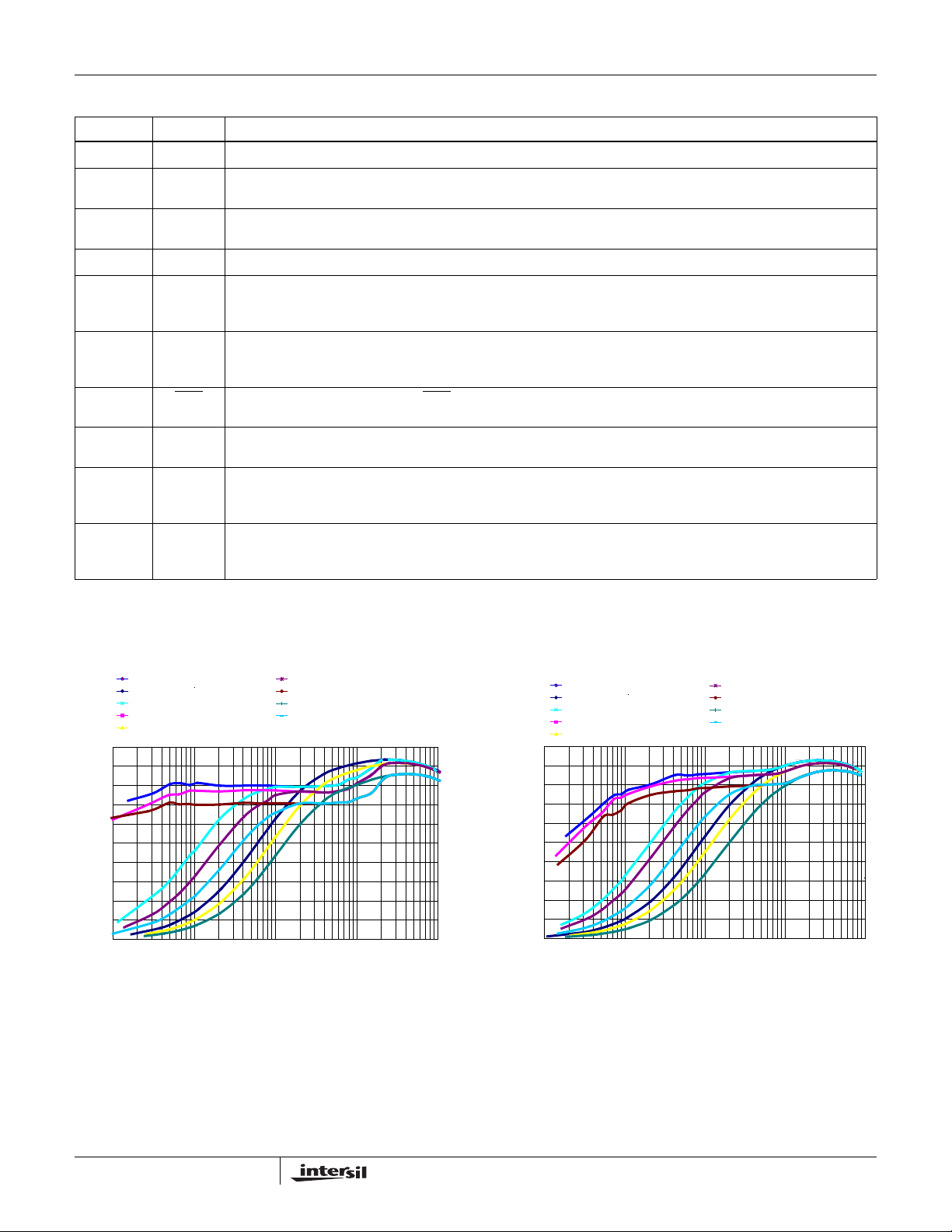
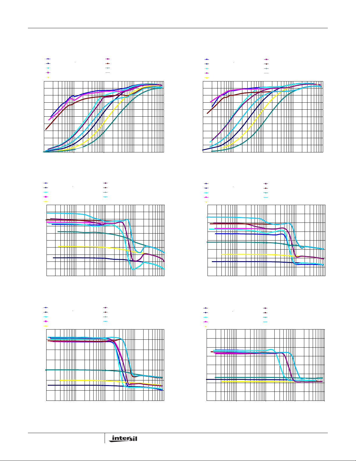
Typical Performance Curves Circuit of Figures 62, 63 and 64, no load on LDO, OUT1, OUT2, and REF, V
7 VIN SKIP MODE
7 VIN PWM MODE
7 VIN ULTRA SKIP MODE
12 VIN SKIP MODE
12 V
PWM MODE
100
90
80
70
60
50
40
EFFICIENCY (%)
30
20
10
0
0.001 0.010 0.100
FIGURE 1. V
IN
OUTPUT LOAD (A)
= 1.05V EFFICIENCY vs LOAD (300kHz) FIGURE 2. V
OUT2
EN2 = EN1 = VCC, VBYP = 5V, PVCC = 5V, V
otherwise noted. Typical values are at T
12 V
ULTRA SKIP MODE
IN
25 VIN SKIP MODE
25 VIN PWM MODE
ULTRA SKIP MODE
25 V
IN
1.000
10.000
EN_LDO
= +25°C.
A
7 VIN SKIP MODE
7 VIN PWM MODE
7 VIN ULTRA SKIP MODE
12 VIN SKIP MODE
PWM MODE
12 V
100
90
80
70
60
50
40
30
EFFICIENCY (%)
20
10
0
0.001
IN
OUT1
=5V, TA= -40°C to +100°C, unless
12 V
IN
25 VIN SKIP MODE
25 VIN PWM MODE
25 V
IN
0.010 0.100 1.000 10.000
OUTPUT LOAD (A)
= 1.5V EFFICIENCY vs LOAD (200kHz)
=12V,
IN
ULTRA SKIP MODE
ULTRA SKIP MODE
8
FN6418.4
March 18, 2008
ISL6237
Typical Performance Curves Circuit of Figures 62, 63 and 64, no load on LDO, OUT1, OUT2, and REF, V
EN2 = EN1 = VCC, VBYP = 5V, PVCC = 5V, V
otherwise noted. Typical values are at T
7 VIN SKIP MODE
7 VIN PWM MODE
7 VIN ULTRA SKIP MODE
12 VIN SKIP MODE
PWM MODE
12 V
100
90
80
70
60
50
40
30
EFFICIENCY (%)
20
10
0
0.001 0.010 0.100 1.000 10.000
FIGURE 3. V
1.070
1.068
1.066
1.064
1.062
1.060
1.058
1.056
OUTPUT VOLTAGE (V)
1.054
1.052
1.050
FIGURE 5. V
IN
OUTPUT LOAD (A)
= 3.3V EFFICIENCY vs LOAD (500kHz) FIGURE 4.
OUT2
7 VIN SKIP MODE
7 VIN PWM MODE
7 VIN ULTRA SKIP MODE
12 VIN SKIP MODE
12 V
PWM MODE
IN
0.001 0.010 0.100 1.000 10.000
OUTPUT LOAD (A)
= 1.05V REGULATION vs LOAD (300kHz) FIGURE 6. V
OUT2
12 V
ULTRA SKIP MODE
IN
25 VIN SKIP MODE
25 VIN PWM MODE
25 V
ULTRA SKIP MODE
IN
12 V
ULTRA SKIP MODE
IN
25 VIN SKIP MODE
25 VIN PWM MODE
ULTRA SKIP MODE
25 V
IN
EN_LDO
= +25°C. (Continued)
A
7 VIN SKIP MODE
7 VIN PWM MODE
7 VIN ULTRA SKIP MODE
12 VIN SKIP MODE
12 V
PWM MODE
100
90
80
70
60
50
EFFICIENCY (%)
40
30
20
10
0
0.001 0.010 0.100 1.000 10.000
IN
VOUT1
7 VIN SKIP MODE
7 VIN PWM MODE
7 VIN ULT RA SKIP MODE
12 VIN SKIP MODE
12 V
PWM MODE
IN
0.001 0.010 0.100 1.000
OUTPUT VOLTAGE (V)
1.540
1.535
1.530
1.525
1.520
1.515
1.510
1.505
1.500
OUT1
=5V, TA= -40°C to +100°C, unless
12 V
IN
25 VIN SKIP MODE
25 VIN PWM MODE
25 V
IN
OUTPUT LOAD (A)
= 5V EFFICIENCY vs LOAD (400kHz)
12 V
IN
25 VIN SKIP MODE
25 VIN PWM MODE
25 V
IN
OUTPUT LOAD (A)
= 1.5V REGULATION vs LOAD (200kHz)
=12V,
IN
ULTRA SKIP MODE
ULTRA SKIP MODE
ULTRA SKIP MODE
ULTRA SKIP MODE
10.000
7 VIN SKIP MODE
7 VIN PWM MODE
7 VIN ULTRA SKIP MODE
12 VIN SKIP MODE
12 V
PWM MODE
3.38
3.37
3.36
3.35
3.34
3.33
OUTPUT VOLTAGE (V)
3.32
3.31
FIGURE 7. V
IN
0.001 0.010 0.100 1.000 10.000
OUT2
OUTPUT LOAD (A)
= 3.3V REGULATION vs LOAD (500kHz) FIGURE 8. V
12 V
ULTRA SKIP MODE
IN
25 VIN SKIP MODE
25 VIN PWM MODE
ULTRA SKIP MODE
25 V
IN
9
7 VIN SKIP MODE
7 VIN PWM MODE
7 VIN ULTRA SKIP MODE
12 VIN SKIP MODE
PWM MODE
12 V
5.16
5.14
5.12
5.10
5.08
5.06
5.04
OUTPUT VOLTAGE (V)
5.02
5.00
IN
0.001 0.010 0.100 1.000 10.000
OUT1
OUTPUT LOAD (A)
= 5V REGULATION vs LOAD (400kHz)
12 V
ULTRA SKIP MODE
IN
25 VIN SKIP MODE
25 VIN PWM MODE
ULTRA SKIP MODE
25 V
IN
FN6418.4
March 18, 2008
ISL6237
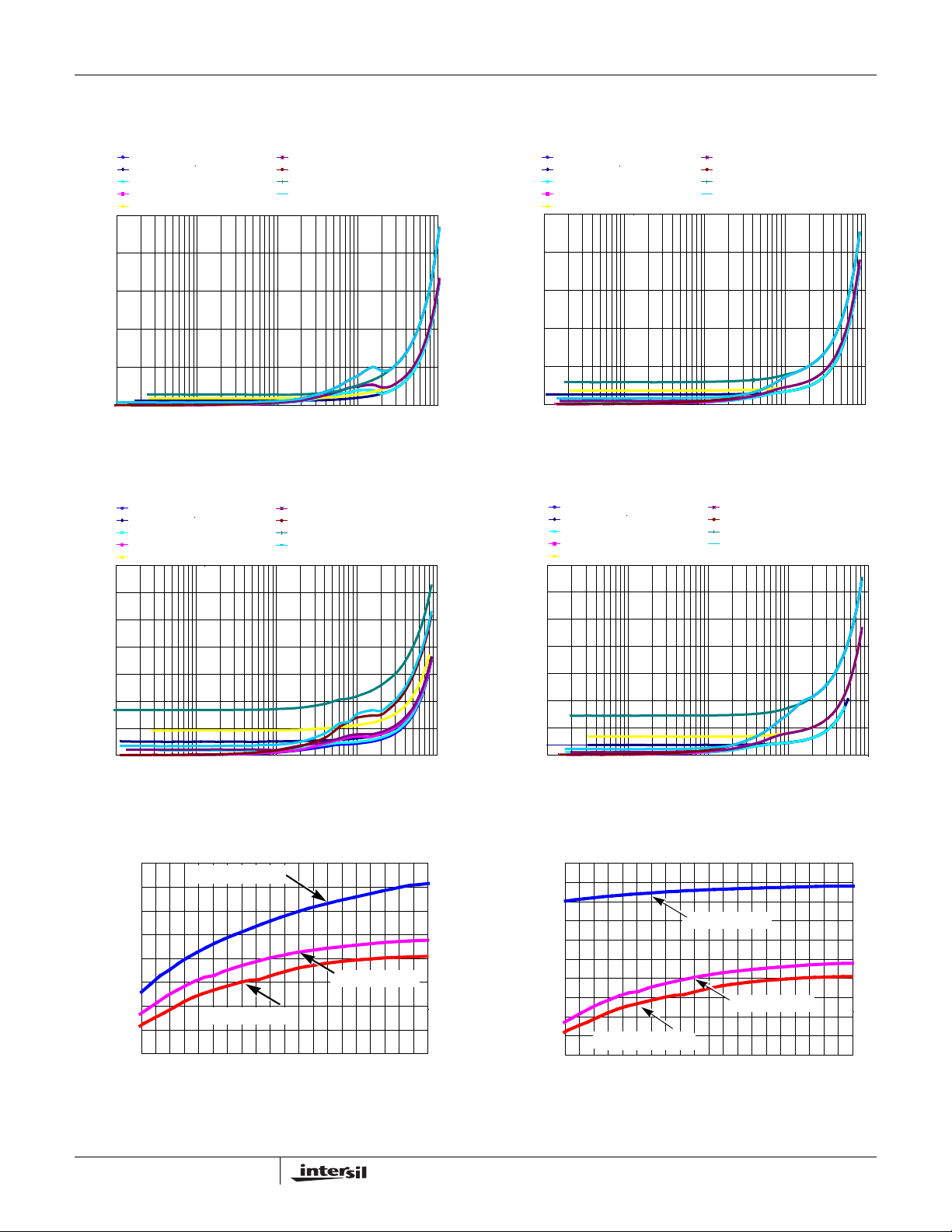
Typical Performance Curves Circuit of Figures 62, 63 and 64, no load on LDO, OUT1, OUT2, and REF, V
EN2 = EN1 = VCC, VBYP = 5V, PVCC = 5V, V
otherwise noted. Typical values are at T
7 VIN SKIP MODE
7 VIN PWM MODE
7 VIN ULTRA SKIP MODE
12 VIN SKIP MODE
PWM MODE
12 V
2.5
2.0
1.5
1.0
0.5
POWER DISSIPATION (W)
0
0.001 0.010 0.100 1.000 10.000
FIGURE 9. V
3.5
IN
OUTPUT LOAD (A)
= 1.05V POWER DISSIPATION vs LOAD
OUT2
(300kHz)
7 VIN SKIP MODE
7 VIN PWM MODE
7 VIN ULTRA SKIP MODE
12 VIN SKIP MODE
PWM MODE
12 V
IN
12 V
ULTRA SKIP MODE
IN
25 VIN SKIP MODE
25 VIN PWM MODE
25 V
ULTRA SKIP MODE
IN
12 V
ULTRA SKIP MODE
IN
25 VIN SKIP MODE
25 VIN PWM MODE
25 V
ULTRA SKIP MODE
IN
EN_LDO
= +25°C. (Continued)
A
7 VIN SKIP MODE
7 VIN PWM MODE
7 VIN ULTRA SKIP MODE
12 VIN SKIP MODE
PWM MODE
12 V
2.5
2.0
1.5
1.0
0.5
POWER DISSIPATION (W)
FIGURE 10. V
3.5
IN
0
0.001 0.010 0.100 1.000 10.000
OUT1
(200kHz)
7 VIN SKIP MODE
7 VIN PWM MODE
7 VIN ULTRA SKIP MODE
12 VIN SKIP MODE
PWM MODE
12 V
IN
=5V, TA= -40°C to +100°C, unless
12 V
IN
25 VIN SKIP MODE
25 VIN PWM MODE
25 V
IN
OUTPUT LOAD (A)
= 1.5V POWER DISSIPA TION vs LOAD
12 V
IN
25 VIN SKIP MODE
25 VIN PWM MODE
25 V
IN
=12V,
IN
ULTRA SKIP MODE
ULTRA SKIP MODE
ULTRA SKIP MODE
ULTRA SKIP MODE
3.0
2.5
2.0
1.5
1.0
POWER DISSIPATION (W)
0.5
0
0.001 0.010 0.100 1.000 10.000
FIGURE 11. V
1.064
1.062
1.060
1.058
1.056
1.054
1.052
OUTPUT VOLTAGE (V)
1.050
1.048
FIGURE 13. V
OUT2
(500kHz)
5791113151719212325
OUT2
vs V
OUTPUT LOAD (A)
= 3.3V POWER DISSIPATION vs LOAD
NO LOAD PWM
MID LOAD PWM
MAX LOAD PWM
INPUT VOLTAGE (V)
= 1.05V OUTPUT VOLTAGE REGULATION
(PWM MODE)
IN
3.0
2.5
2.0
1.5
1.0
POWER DISSIPATION (W)
0.5
0
0.001 0.010 0.100 1.000 10.000
FIGURE 12. V
1.068
1.066
1.064
1.062
1.060
1.058
1.056
1.054
OUTPUT VOLTAGE (V)
1.052
1.050
1.048
FIGURE 14. V
OUT1
(400kHz)
MAX LOAD PWM
MAX LOAD PWM
5791113151719212325
OUT2
vs V
IN
OUTPUT LOAD (A)
= 5V POWER DISSIPA TION vs LOAD
NO LOAD PWM
MID LOAD PWM
INPUT VOLTAGE (V)
= 1.05V OUTPUT VOLT AGE REGULA TION
(SKIP MODE)
10
FN6418.4
March 18, 2008
ISL6237
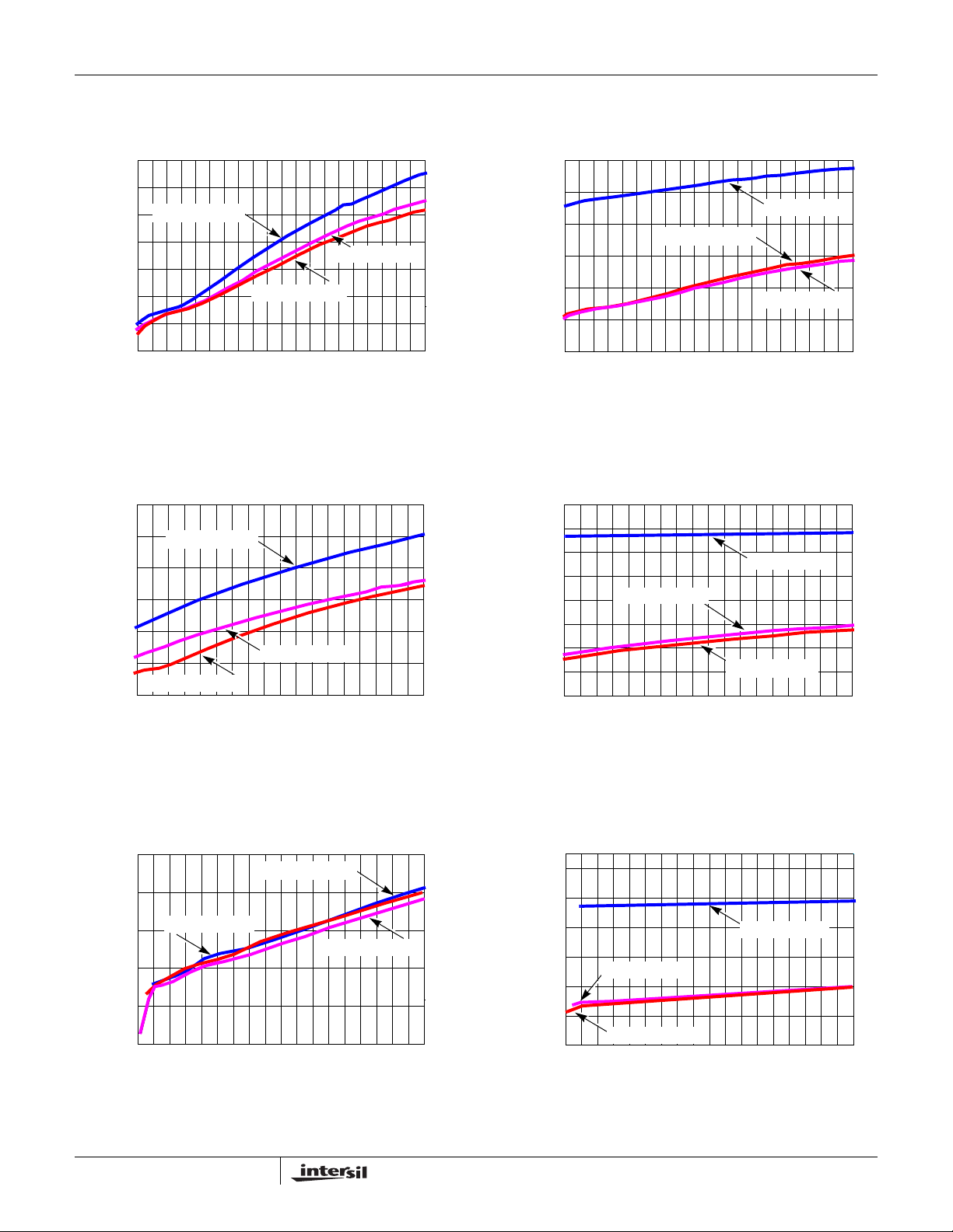
Typical Performance Curves Circuit of Figures 62, 63 and 64, no load on LDO, OUT1, OUT2, and REF, V
1.518
1.516
1.514
1.512
1.510
1.508
OUTPUT VOLTAGE (V)
1.506
1.504
5791113151719212325
FIGURE 15. V
3.340
3.335
3.330
3.325
3.320
OUTPUT VOLTAGE (V)
3.315
3.310
MAX LOAD PWM
7 9 11 13 15 17 19 21 23 25
FIGURE 17. V
EN2 = EN1 = VCC, VBYP = 5V, PVCC = 5V, V
otherwise noted. Typical values are at T
NO LOAD PWM
MID LOAD PWM
MAX LOAD PWM
INPUT VOLTAGE (V)
= 1.5V OUTPUT VOLTAGE REGULA TION
OUT1
vs V
(PWM MODE)
IN
NO LOAD PWM
MID LOAD PWM
INPUT VOLTAGE (V)
= 3.3V OUTPUT VOLTAGE REGULA TION
OUT2
vs V
(PWM MODE)
IN
= +25°C. (Continued)
A
1.530
1.525
1.520
1.515
1.510
OUTPUT VOLTAGE (V)
1.505
1.500
5791113151719212325
FIGURE 16. V
3.38
3.37
3.36
3.35
3.34
3.33
3.32
OUTPUT VOLTAGE (V)
3.31
3.30
7 9 11 13 15 17 19 21 23 25
FIGURE 18. V
EN_LDO
OUT1
vs V
OUT2
vs V
=5V, TA= -40°C to +100°C, unless
MID LOAD PWM
INPUT VOLTAGE (V)
= 1.5V OUTPUT VOLT AGE REGULA TION
(SKIP MODE)
IN
NO LOAD PWM
MAX LOAD PWM
MID LOAD PWM
INPUT VOLTAGE (V)
= 3.3V OUTPUT VOLTAGE REGULA TION
(SKIP MODE)
IN
=12V,
IN
NO LOAD PWM
MAX LOAD PWM
5.065
5.060
5.055
5.050
OUTPUT VOLTAGE (V)
5.045
5.040
7 9 11 13 15 17 19 21 23 25
FIGURE 19. V
NO LOAD PWM
MAX LOAD PWM
MID LOAD PWM
INPUT VOLTAGE (V)
= 5V OUTPUT VOLT AGE REGULA TION vs
OUT1
V
(PWM MODE)
IN
11
5.14
5.12
5.10
5.08
5.06
OUTPUT VOLTAGE (V)
5.04
5.02
7 9 11 13 15 17 19 21 23 25
FIGURE 20. V
NO LOAD PWM
MID LOAD PWM
MAX LOAD PWM
INPUT VOLTAGE (V)
= 5V OUTPUT VOLT AGE REGULA TION vs
OUT1
V
(SKIP MODE)
IN
FN6418.4
March 18, 2008

ISL6237
Typical Performance Curves Circuit of Figures 62, 63 and 64, no load on LDO, OUT1, OUT2, and REF, V
EN2 = EN1 = VCC, VBYP = 5V, PVCC = 5V, V
otherwise noted. Typical values are at T
300
250
200
150
100
FREQUENCY (kHz)
50
FIGURE 21. V
250
200
150
100
FREQUENCY (kHz)
50
0
ULTRA-SKIP
0
0.001 0.010 0.100 1.000 10.000
OUTPUT LOAD (A)
= 1.05V FREQUENCY vs LOAD FIGURE 22. V
OUT2
PWM
ULTRA-SKIP
SKIP
0.001 0.010 0.100 1.000 10.000
OUTPUT LOAD (A)
PWM
SKIP
EN_LDO
= +25°C. (Continued)
A
50
45
40
35
30
25
20
RIPPLE (mV)
15
10
5
0
0.001 0.010 0.100 1.000 10.000
50
45
40
35
30
25
ULTRA-SKIP
20
RIPPLE (mV)
15
10
5
0
0.001 0.010 0.100 1.000 10.000
=5V, TA= -40°C to +100°C, unless
PWM
OUTPUT LOAD (A)
= 1.05V RIPPLE vs LOAD
OUT2
SKIP
OUTPUT LOAD (A)
=12V,
IN
ULTRA-SKIP
SKIP
PWM
FIGURE 23. V
600
500
400
300
200
FREQUENCY (kHz)
100
SKIP
0
0.001 0.010 0.100 1.000 10.000
FIGURE 25. V
= 1.5V FREQUENCY vs LOAD FIGURE 24. V
OUT1
PWM
ULTRA-SKIP
OUTPUT LOAD (A)
= 3.3V FREQUENCY vs LOAD FIGURE 26. V
OUT2
12
= 1.5V RIPPLE vs LOAD
OUT1
14
12
10
8
6
RIPPLE (mV)
4
2
0
0.001 0.010 0.100 1.000 10.000
PWM
ULTRA-SKIP
OUTPUT LOAD (A)
= 3.3V RIPPLE vs LOAD
OUT2
SKIP
March 18, 2008
FN6418.4

ISL6237
Typical Performance Curves Circuit of Figures 62, 63 and 64, no load on LDO, OUT1, OUT2, and REF, V
450
400
350
300
250
200
150
FREQUENCY (kHz)
100
50
ULTRA-SKIP
0
0.001 1.000
0.010 0.100
FIGURE 27. V
5.04
5.02
5.00
4.98
4.96
4.94
4.92
4.90
4.88
OUTPUT VOLTAGE (V)
4.86
4.84
0 50 100 150 200
PWM
SKIP
OUTPUT LOAD (A)
= 5V FREQUENCY vs LOAD FIGURE 28. V
OUT1
BYP = 0V
BYP = 5V
OUTPUT LOAD (mA)
EN2 = EN1 = VCC, VBYP = 5V, PVCC = 5V, V
otherwise noted. Typical values are at T
RIPPLE (mV)
10.000
= +25°C. (Continued)
A
40
35
30
ULTRA-SKIP
25
20
15
10
5
0
0.001 0.010 0.100 1.000 10.000
3.35
3.30
3.25
3.20
3.15
3.10
OUTPUT VOLTAGE (V)
3.05
3.00
0 50 100 150 200
EN_LDO
=5V, TA= -40°C to +100°C, unless
PWM
SKIP
OUTPUT LOAD (A)
= 5V RIPPLE vs LOAD
OUT1
BYP = 0V
BYP = 3.3V
OUTPUT LOAD (mA)
IN
=12V,
FIGURE 29. LDO OUTPUT 5V vs LOAD FIGURE 30. LDO OUTPUT 3.3V vs LOAD
50
45
40
35
30
INPUT CURRENT (mA)
25
20
7 9 11 13 15 17 19 21 23 25
INPUT VOLTAGE (V)
FIGURE 31. PWM NO LOAD INPUT CURRENT vs V
(EN = EN2 = EN_LDO = VCC)
13
IN
1400
1200
1000
800
600
400
INPUT CURRENT (µA)
200
0.0
7 9 11 13 15 17 19 21 23 25
INPUT VOLTAGE (V)
FIGURE 32. SKIP NO LOAD INPUT CURRENT vs V
(EN1 = EN2 = EN_LDO = VCC)
IN
FN6418.4
March 18, 2008

ISL6237
Typical Performance Curves Circuit of Figures 62, 63 and 64, no load on LDO, OUT1, OUT2, and REF, V
177.5
177.0
176.5
176.0
175.5
175.0
174.5
174.0
INPUT CURRENT (µA)
173.5
173.0
7 9 11 13 15 17 19 21 23 25
INPUT VOLTAGE (V)
FIGURE 33. STANDBY INPUT CURRENT vs V
(EN = EN2 = 0, EN_LDO = VCC)
EN1 5V/DIV
EN2 = EN1 = VCC, VBYP = 5V, PVCC = 5V, V
otherwise noted. Typical values are at T
IN
V
OUT1
FIGURE 34. SHUTDOWN INPUT CURRENT vs V
2V/DIV
= +25°C. (Continued)
A
26.5
26.0
25.5
25.0
24.5
24.0
23.5
23.0
INPUT CURRENT (µA)
22.5
22.0
7 9 11 13 15 17 19 21 23 25
(EN = EN2 = EN_LDO = 0)
EN_LDO
=5V, TA= -40°C to +100°C, unless
INPUT VOLTAGE (V)
IN
=12V,
IN
IL1 2A/DIV
POK1 2V/DIV
EN1 5V/DIV
V
OUT1
IL1 2A/DIV
POK1 2V/DIV
FIGURE 35. START-UP V
2V/DIV
= 5V (NO LOAD, SKIP MODE)
OUT1
IL1 5A/DIV
POK1 2V/DIV
EN1 5V/DIV
V
OUT1
2V/DIV
FIGURE 36. START-UP V
= 5V (NO LOAD, PWM MODE) FIGURE 37. START-UP V
OUT1
14
= 5V (FULL LOAD, PWM MODE)
OUT1
FN6418.4
March 18, 2008

ISL6237
Typical Performance Curves Circuit of Figures 62, 63 and 64, no load on LDO, OUT1, OUT2, and REF, V
EN2 5V/DIV
V
OUT2
IL2 2A/DIV
FIGURE 38. START-UP V
EN2 = EN1 = VCC, VBYP = 5V, PVCC = 5V, V
otherwise noted. Typical values are at T
2V/DIV
POK2 2V/DIV
= 3.3V (NO LOAD, SKIP MODE) FIGURE 39. START-UP V
OUT2
= +25°C. (Continued)
A
EN_LDO
EN2 5V/DIV
=5V, TA= -40°C to +100°C, unless
V
2V/DIV
OUT2
IL2 2A/DIV
= 3.3V (NO LOAD, PWM MODE)
OUT1
=12V,
IN
POK2 2V/DIV
EN2 5V/DIV
V
2V/DIV
OUT2
IL2 5A/DIV
POK2 2V/DIV
FIGURE 40. START - UP V
PWM MODE)
EN1 5V/DIV
POK1 5V/DIV
V
= 3.3V (FULL LOAD,
OUT1
2V/DIV
OUT2
V
OUT1
2V/DIV
EN2 5V/DIV
V
2V/DIV
OUT2
2V/DIV
V
OUT1
POK2 5V/DIV
POK1 5V/DIV
FIGURE 41. DELAYED ST ART -UP (V
EN1 = REF)
EN1 5V/DIV
V
2V/DIV
OUT2
V
2V/DIV
OUT1
OUT1
=5V, V
OUT2
=3.3V,
POK2 5V/DIV
FIGURE 42. DELAYED ST ART -UP (V
EN2 = REF)
15
OUT1
=5V, V
OUT2
=3.3V,
POK1 OR POK2 5V/DIV
FIGURE 43. SHUTDOWN (V
EN2 = REF)
OUT1
=5V, V
OUT2
=3.3V,
March 18, 2008
FN6418.4

ISL6237
Typical Performance Curves Circuit of Figures 62, 63 and 64, no load on LDO, OUT1, OUT2, and REF, V
LGATE1 5V/DIV
RIPPLE 50mV/DIV
V
OUT1
IL1 5A/DIV
V
RIPPLE 50mV/DIV
OUT2
FIGURE 44. LOAD TRANSIENT V
LGATE1 5V/DIV
EN2 = EN1 = VCC, VBYP = 5V, PVCC = 5V, V
otherwise noted. Typical values are at T
= 5V FIGURE 45. LOAD TRANSIENT V
OUT1
EN_LDO
= +25°C. (Continued)
A
=5V, TA= -40°C to +100°C, unless
LGATE1 5V/DIV
V
RIPPLE 100mV/DIV
OUT1
IL1 5A/DIV
V
RIPPLE 50mV/DIV
OUT2
OUT1
LGATE2 5V/DIV
=12V,
IN
= 5V (SKIP)
V
RIPPLE 20mV/DIV
OUT1
IL2 5A/DIV
V
RIPPLE 50mV/DIV
OUT2
FIGURE 46. LOAD TRANSIENT V
V
RIPPLE 20mV/DIV
OUT
LDO 1V/DIV
LDOREFIN 0.5V/DIV
IL2 5A/DIV
V
RIPPLE 50mV/DIV
OUT2
= 3.3V (PWM) FIGURE 47. LOAD TRANSIENT V
OUT1
EN1 5V/DIV
0.5V/DIV
V
OUT1
V
RIPPLE 20mV/DIV
OUT1
= 3.3V (SKIP)
OUT1
IL1 2A/DIV
V
RIPPLE 50mV/DIV
OUT2
POK1 2V/DIV
FIGURE 48. LDO TRACKING TO LDOREFIN FIGURE 49. START-UP V
16
= 1.5V (NO LOAD, SKIP MODE)
OUT1
FN6418.4
March 18, 2008

ISL6237
Typical Performance Curves Circuit of Figures 62, 63 and 64, no load on LDO, OUT1, OUT2, and REF, V
EN1 5V/DIV
V
0.5V/DIV
OUT1
IL1 2A/DIV
POK1 2V/DIV
FIGURE 50. START-UP V
EN2 5V/DIV
EN2 = EN1 = VCC, VBYP = 5V, PVCC = 5V, V
otherwise noted. Typical values are at T
= 1.5V (NO LOAD, PWM MODE)S
OUT1
EN_LDO
= +25°C. (Continued)
A
EN1 5V/DIV
POK1 2V/DIV
FIGURE 51. START-UP V
PWM MODE)
EN2 5V/DIV
=5V, TA= -40°C to +100°C, unless
V
0.5V/DIV
OUT1
IL1 5A/DIV
= 1.5V (FULL LOAD,
OUT1
IN
=12V,
V
0.5V/DIV
OUT2
IL2 2A/DIV
POK2 2V/DIV
FIGURE 52. START - UP V
SKIP MODE)
EN2 5V/DIV
IL2 2A/DIV
= 1.05V (NO LOAD,
OUT2
V
OUT2
0.5V/DIV
V
0.5V/DIV
OUT2
IL2 2A/DIV
POK2 2V/DIV
FIGURE 53. START-UP V
PWM MODE)
EN2 5V/DIV
V
0.5V/DIV
OUT2
V
2V/DIV
OUT1
POK2 5V/DIV
= 1.05V (NO LOAD,
OUT1
POK2 2V/DIV
FIGURE 54. START - UP V
PWM MODE)
= 1.05V (FULL LOAD,
OUT1
17
POK1 5V/DIV
FIGURE 55. DELAYED ST ART -UP (V
V
= 1.05V, EN1 = REF)
OUT2
OUT1
=1.5V,
FN6418.4
March 18, 2008

ISL6237
Typical Performance Curves Circuit of Figures 62, 63 and 64, no load on LDO, OUT1, OUT2, and REF, V
V
2V/DIV
OUT1
EN1 500mV/DIV
V
500mV/DIV
OUT2
POK1 5V/DIV
POK2 5V/DIV
FIGURE 56. DELA YED START -UP (V
V
= 1.05V, EN2 = REF)
OUT2
LGATE1 5V/DIV
OUT1
EN2 = EN1 = VCC, VBYP = 5V, PVCC = 5V, V
otherwise noted. Typical values are at T
V
OUT1
=1.5V,
FIGURE 57. SHUTDOWN (V
EN_LDO
= +25°C. (Continued)
A
V
2V/DIV
POK1 OR POK2 5V/DIV
EN2 = REF)
=5V, TA= -40°C to +100°C, unless
EN1 5V/DIV
2V/DIV
OUT2
=1.5V, V
OUT1
LGATE1 5V/DIV
IN
OUT2
=12V,
= 1.05V,
V
RIPPLE 50mV/DIV
OUT1
IL1 5A/DIV
V
RIPPLE 20mV/DIV
OUT2
FIGURE 58. LOAD TRANSIENT V
LGATE2 5V/DIV
V
RIPPLE 20mV/DIV
OUT1
IL1 5A/DIV
V
RIPPLE 50mV/DIV
OUT1
IL1 5A/DIV
= 1.5V (PWM) FIGURE 59. LOAD TRANSIENT V
OUT1
LGATE2 5V/DIV
V
RIPPLE 20mV/DIV
OUT1
V
RIPPLE 20mV/DIV
OUT2
V
RIPPLE 20mV/DIV
OUT2
= 1.5V (SKIP)
OUT1
IL2 5A/DIV
V
RIPPLE 20mV/DIV
OUT2
FIGURE 60. LOAD TRANSIENT V
18
= 1.05V (PWM) FIGURE 61. LOAD TRANSIENT V
OUT1
= 1.05V (SKIP)
OUT1
FN6418.4
March 18, 2008

ISL6237
Typical Application Circuits
The typical application circuits (Figures 62, 63 and 64)
generate the typical 5V/7A, 3.3V/11A, 1.25V/5A, static
voltage/10A, 1.5V/5A, and 1.05V/5A supplies found in a
notebook computer. The input supply range is 5.5V to 25V.
Detailed Description
The ISL6237 dual-buck, BiCMOS, switch-mode powersupply controller generates logic supply voltages for
notebook computers. The ISL6237 is designed primarily for
battery-powered applications where high efficiency and lowquiescent supply current are critical. The ISL6237 provides a
pin-selectable switching frequency, allowing operation for
200kHz/300kHz, 400kHz/300kHz, or 400kHz/500kHz on the
SMPSs.
Light-load efficiency is enhanced by automatic Idle-Mode
operation, a variable-frequency pulse-skipping mode that
reduces transition and gate-charge losses. Each step-down,
power-switching circuit consists of two N-Channel
MOSFETs, a rectifier, and an LC output filter. The output
voltage is the average AC voltage at the switching node,
which is regulated by changing the duty cycle of the
MOSFET switches. The gate-drive signal to the N-Channel
high-side MOSFET must exceed the battery voltage, and is
provided by a flying-capacitor boost circuit that uses a 100nF
capacitor connected to BOOT_.
Both SMPS1 and SMPS2 PWM controllers consist of a triplemode feedback network and multiplexer, a multi-in put PWM
comparator, high -side and low -side gate drivers and lo gic. In
addition, SMPS2 can also use REFIN2 to track its output from
0.5V to 2.5V. The ISL6237 contains fault-protection circuits
that monitor the main PWM outputs for undervoltage and
overvoltage conditions. A power-on sequence block controls
the power-up timing of the main PWMs and monitors the
outputs for undervoltage faults . The ISL6237 in cludes an
adjustable low drop-out linear regulator. The bias generator
blocks include the linear regulator , a 2V precision reference
and automatic bootstrap switchover circuit.
The synchronous-switch gate drivers are directly powered
from PVCC, while the high-side switch gate drivers are
indirectly powered from PVCC through an external capacitor
and an internal Schottky diode boost circuit.
An automatic bootstrap circuit turns off the LDO linear
regulator and powers the device from BYP if LDOREFIN is
set to GND or VCC. See Table 1.
TABLE 1. LDO OUTPUT VOLTAGE TABLE
LDO VOLTAGE CONDITIONS COMMENT
VOLTAGE at BYP LDOREFIN < 0.3V,
BYP > 4.63V
VOLTAGE at BYP LDOREFIN > VCC - 1V,
BYP > 3V
5V LDOREFIN < 0.3V,
BYP < 4.63V
Internal LDO is
disabled.
Internal LDO is
disabled.
Internal LDO is
active.
TABLE 1. LDO OUTPUT VOLTAGE TABLE (Continued)
LDO VOLTAGE CONDITIONS COMMENT
3.3V LDOREFIN > VCC - 1V,
BYP < 3V
2 x LDOREFIN 0.35V < LDOREFIN < 2.25V Internal LDO is
Internal LDO is
active.
active.
FREE-RUNNING, CONSTANT ON-TIME PWM
CONTROLLER WITH INPUT FEED-FORWARD
The constant on-time PWM control architecture is a
pseudo-fixed-frequency, constant on-time, current-mode
type with voltage feed forward. The constant on-time PWM
control architecture relies on the output ripple voltage to
provide the PWM ramp signal; thus the output filter
capacitor's ESR acts as a current-feedback resistor. The
high-side switch on-time is determined by a one-shot whose
period is inversely proportional to input voltage and directly
proportional to output voltage. Another one-shot sets a
minimum off-time (300ns typ). The on-time one-shot triggers
when the following conditions are met: the error comp ara to r' s
output is high, the synchronous rectifier current is below the
current-limit threshold, and the minimum off time one-shot
has timed out. The controller utilizes the valley point of the
output ripple to regulate and determine the off time.
On-Time One-Shot (t
ON
)
Each PWM core includes a one-shot that sets the high-side
switch on-time for each controller. Each fast, low-jitter,
adjustable one-shot includes circuitry that varies the on-time
in response to battery and output voltage. The high-side
switch on-time is inversely proportional to the battery voltage
as measured by the VIN input and proportional to the output
voltage. This algorithm results in a nearly constant switching
frequency despite the lack of a fixed-frequency clock
generator. The benefit of a constant switching frequency is
that the frequency can be selected to avoid noise-sensitive
frequency regions:
KV
OUTILOADrDSON LOWERQ()
------------------------------------------------------------------------------------------------------
t
=
ON
⋅+()
V
IN
(EQ. 1)
See Table 2 for approximate K- factors. Switching frequency
increases as a function of load current due to the increasing
drop across the synchronous rectifier, which causes a faster
inductor-current discharge ramp. On-times translate only
roughly to switching frequencies. The on-times established in
the “Electrical Specifications” table o n p age4 are influenced
by switching delays in the external high-side power MOSFET.
Also, the dead-time effect increases the effective on-time,
reducing the switching frequency . It occurs only in PWM mode
(SKIP
= VCC) and during dynamic output voltage transitions
when the inductor current reverses at light or negative load
currents. With reversed inductor current, the inductor's EMF
causes PHASE to go high earlier than normal, extending the
on-time by a period equal to the UGA TE-rising dead time.
19
FN6418.4
March 18, 2008

ISL6237
.
TABLE 2. APPROXIMATE K-FACTOR ERRORS
SMPS
(t
= GND, REF,
ON
or OPEN), VOUT1
(t
= GND),
ON
VOUT2
(t
= VCC),
ON
VOUT1
= VCC, REF,
(t
ON
or OPEN), VOUT2
SWITCHING
FREQUENCY
(kHz)
400 2.5 ±10
500 2.0 ±10
200 5.0 ±10
300 3.3 ±10
K-FACTOR
(µs)
APPROXIMATE
K-FACTOR
ERROR (%)
For loads above the critical conduction point, the actual
switching frequency is:
+
V
OUTVDROP1
-------------------------------------------------------
f
=
t
ONVINVDROP2
+()
(EQ. 2)
where:
•V
is the sum of the parasitic voltage drops in the
DROP1
inductor discharge path, including synchronous rectifier,
inductor, and PC board resistances
•V
DROP2
is the sum of the parasitic voltage drops in the
charging path, including high-side switch, inductor, and PC
board resistances
•t
is the on-time calculated by the ISL6237
ON
20
FN6418.4
March 18, 2008

OUT1 – PCI-e
1.25V/5A
C
C
11
330µF
9mΩ
6.3V
VIN: 5.5V TO 25V
C
10
10µF
SI4816BDY
L1: 3.3µH
R1
7.87kΩ
R
10kΩ
Q3a
Q3b
FB1 TIED TO GND = 5V
FB1 TIED TO VCC = 1.5V
2
VCC
C
0.1µF
5V
C
1µF
9
R
3
200kΩ
ISL6237
5V
8
PVCC
VIN
BOOT1
UGATE1
PHASE1
LGATE1
OUT1
EN1
BYP
FB1
AGND
ILIM1
SKIP
EN_LDO
C
5
1µF
VCC
ISL6237
LDO
LDOREFIN
BOOT2
UGATE2
PHASE2
LGATE2
PGND
OUT2
EN2
REFIN2
ILIM2
REF
R
5
200kΩ
NC
GND
C
4
0.22µF
VCC
C
7
0.1µF
C1
C1
10
10µF
Q
1
IRF7821
L2: 2.2µH
Q
2
IRF7832
REFIN2: STATIC 0V TO 2.5V
REFIN2 TIED TO 3.3V = 1.05V
REFIN2 TIED TO VCC = 3.3V
VCC
OUT2-GFX
TRACK REFIN2/10A
C
C
2
2 x 330µF
4mΩ
6.3V
VCC
R
4
200kΩ 200kΩ
R
6
POK1
VCC
TON
POK2
PAD
FREQUENCY-DEPENDENT COMPONENTS
t
1.25V/1.05V SMPS
SWITCHING
FREQUENCY
L
1
L
2
C
2
C
11
3.3µH
2.7µH
2 x 330µF
330µF
=VCC
ON
200kHz/300kHz
FIGURE 62. ISL6237 TYPICAL GFX APPLICATION CIRCUIT
21
FN6418.4
March 18, 2008

C
C
11
330µF
9mΩ
6.3V
VIN: 5.5V TO 25V
C
10
10µF
OUT1
1.5V/5A
L1: 3.3µH
FB1 TIED TO GND= 5V
FB1 TIED TO VCC = 1.5V
SI4816BDY
Q3a
Q3b
VCC
3.3V
VCC
0.1µF
ON
C
VCC
C
1µF
9
R
3
200kΩ
OFFONOFFOFF
ISL6237
5V
8
PVCC
VIN
BOOT1
UGATE1
PHASE1
LGATE1
OUT1
EN1
BYP
FB1
AGND
ILIM1
SKIP
EN_LDO
TON
C
1µF
VCC
ISL6237
PAD
5
LDO
LDOREFIN
BOOT2
UGATE2
PHASE2
LGATE2
PGND
OUT2
EN2
REFIN2
ILIM2
REF
POK1
POK2
VCC
Q1a
C
4
0.22µF
Q1b
VCC
REFIN2: STATIC 0V TO 2.5V
REFIN2 TIED TO 3.3V = 1.05V
R
REFIN2 TIED TO VCC = 3.3V
5
200kΩ
C7
0.1µF
LDOREFIN TIED TO GND = 5V
LDOREFIN TIED TO VCC = 3.3V
C
C
1
10
10µF
L2: 2.2µF
SI4816BDY
VCC
R
200kΩ
LDO
4
C
6
4.7µF
OUT2
1.05V/5A
C
C
330µF
4mΩ
6.3V
VCC
F
2
R
6
200kΩ
FREQUENCY-DEPENDENT COMPONENTS
1.5V/1.05V SMPS
SWITCHING
FREQUENCY
L
1
L
2
C
2
C
11
I
FIGURE 63. ISL6237 TYPICAL SYSTEM REGULATOR APPLICATION CIRCUIT
22
t
=VCC
ON
200kHz/300kHz
3.3µH
2.7µH
330µF
330µF
FN6418.4
March 18, 2008

VIN: 5.5V TO 25V
ISL6237
C5
1µF
C11
330µF
9mΩ
6.3V
OUT1
5V/7A
C10
10µF
IRF7807V
L1: 4.7µH
IRF7811AV
Q3
C9
C9
0.1µF
Q4
FB1 TIED TO GND = 5V
FB1 TIED TO VCC = 1.5V
ON
GND
VCC
200kΩ
OFFONOFFOFF
R3
PVCC
VIN
BOOT1
UGATE1
PHASE1
LGATE1
OUT1
EN1
BYP
FB1
AGND
ILIM1
SKIP
EN LDO
TON
VCC
ISL6237
PAD
LDO
LDOREFIN
BOOT2
UGATE2
PHASE2
LGATE2
PGND
OUT2
EN2
REFIN2
ILIM2
REF
POK1
POK2
R5
150kΩ
C1
C1
10µF
10
Q1
C4
0.1µF
VCC
VCC
0.1µF
C7
IRF7821
L2: 4.7µH
Q2
IRF7832
REFIN2: STATIC 0 TO 2.5V
REFIN2 TIED TO VREF3 = 1.05V
REFIN2 TIED TO VCC = 3.3V
VCC
LDO
R4
200kΩ
C6
4.7µF
OUT2
3.3V/11A
C2
C2
330µF
VCC
R6
200kΩ
9mΩ
4V
FIGURE 64. ISL6237 TYPICAL 3.3V/5V SYSTEM REGULATOR APPLICATION CIRCUIT
23
FN6418.4
March 18, 2008

ISL6237
BOOT1
UGATE1
PHASE1
LGATE1
GND
ILIM1
FB1
OUT1
BYP
PVCC
SMPS1
SYNCHRONOUS
PWM BUCK
CONTROLLER
OUT1
SW THRESHOLD
-
-+-
+
+
EN1
POK1
TON
SKIP
SMPS2
SYNCHRONOUS
PWM BUCK
CONTROLLER
EN2
POK2
OUT2
BOOT2
UGATE2
PHASE2
PVCC
LGATE2
PGND
ILIM2
REFIN2
OUT2
POK2
POK1
LDO
LDOREFIN
VIN
EN_LDO
EN1
EN2
LDO
POWER-ON
SEQUENCE
CLEAR FAULT
LATCH
THERMAL
THERMAL
SHUTDOWN
SHUTDOWN
FIGURE 65. DETAILED FUNCTIONAL DIAGRAM ISL6237
INTERNAL
LOGIC
REF
VCC
Ω
10
PVCC
REF
24
FN6418.4
March 18, 2008

ISL6237
VIN
ILIM_
PHASE_
OUT_
FB_
VCC
TON
5µA
DECODER
OUT_
REFIN2 (SMPS2)
VREF
+
+
SLOPE COMP
FB
MIN. t
OFF
TRIG
Q
ONE SHOT
+
++
+
+
+
+
+
COMP
+
+
S
+
+
+
++
SKIP
+
++
+
++
OV_LATCH_
UV_LATCH_
+
+
+
PGOOD_
20ms
BLANKING
0.9V
1.1V
0.7V
REF
REF
REF
BOOT
DETECT
Q
Q
Q
S
S
S
R
R
R
Q
Q
Q
R
R
R
S
S
S
UV
FAULT
FAULT
LATCH
LATCH
LOGIC
TO UGATE_DRIVER
Q
Q
Q
Q
BOOT_
TO LGATE_ DRIVER
FIGURE 66. PWM CONTROLLER (ONE SIDE ONLY)
25
FN6418.4
March 18, 2008

ISL6237
Automatic Pulse-Skipping Switchover
(Idle Mode)
In Idle Mode (SKIP = GND), an inherent automatic
switchover to PFM takes place at light loads. This switchover
is affected by a comparator that truncates the low-side
switch on-time at the inductor current's zero crossing. This
mechanism causes the threshold between pulse-skipping
PFM and non skipping PWM operation to coincide with the
boundary between continuous and discontinuous
inductor-current operation (also known as the critical
conduction point):
KV
⋅
VINV
OUT
I
LOAD SKIP()
------------------------
=
2L⋅
where K is the on-time scale factor (see “On- Time One-Shot
(t
” on page 19). The load-current level at which
ON)
PFM/PWM crossover occurs, I
the peak-to-peak ripple current, which is a function of the
inductor value (Figure 67). For example, in the ISL6237
typical application circuit with V
L = 7.6µH, and K = 5µs, switchover to pulse-skipping
operation occurs at I
LOAD
The crossover point occurs at an even lower value if a
swinging (soft-saturation) inductor is used.
I
D
VIN-V
VIN-V
VIN-V
V-V
=
=
=
=
t
t
t
t
L
L
L
OUT
–
OUT
------------------------------- -
V
IN
LOAD(SKIP)
OUT1
, is equal to half
=5V, VIN=12V,
= 0.96A or about on-fifth full load.
I
PEAK
I
= I
LOAD
(EQ. 3)
PEAK/2
The switching waveforms may appear noisy and
asynchronous when light loading causes pulse-skipping
operation, but this is a normal operating condition that
results in high light-load efficiency. Trade-offs in PFM noise
vs light-load efficiency are made by varying the inductor
value. Generally, low inductor values produce a broader
efficiency vs load curve, while higher values result in higher
full-load efficiency (assuming that the coil resistance remains
fixed) and less output voltage ripple. Penalties for using
higher inductor values include larger physical size and
degraded load-transient response (especially at low
input-voltage levels).
DC output accuracy specifications refer to the trip level of the
error comparator. When the inductor is in continuous
conduction, the output voltage has a DC regulation higher
than the trip level by 50% of the ripple. In discontinuous
conduction (SKIP
= GND, light load), the output voltage has
a DC regulation higher than the trip level by approximately
1.0% due to slope compensation.
Forced-PWM Mode
The low-noise, forced-PWM (SKIP = VCC) mode disables
the zero-crossing comparator, which controls the low-side
switch on-time. Disabling the zero-crossing detector causes
the low-side, gate-drive waveform to become the
complement of the high-side, gate-drive waveform. The
inductor current reverses at light loads as the PWM loop
strives to maintain a duty ratio of V
OUT/VIN
forced-PWM mode is to keep the switching frequency fairly
constant, but it comes at a cost: the no-load battery current
can be 10mA to 50mA, depending on switching frequency
and the external MOSFETs.
. The benefit of
INDUCTOR CURRENT
ON-TIME TIME
0
FIGURE 67. ULTRASONIC CURRENT WAVEFORMS
40µs (MAX)
INDUCTOR
Zero-Crossing
ZERO-CROSSING
DETECTION
0A
FB < REG .POINT
ON-TIME (t
ON-TIME (tON)
FIGURE 68. ULTRASONIC CURRENT WAVEFORMS
CURRENT
Forced-PWM mode is most useful for reducing
audio-frequency noise, improving load-transient response,
providing sink-current capability for dynamic output voltage
adjustment, and improving the cross-regulation of
multiple-output applications that use a flyback transformer or
coupled inductor.
Enhanced Ultrasonic Mode
(25kHz (min) Pulse Skipping)
Leaving SKIP unconnected or connecting SKIP to REF
activates a unique pulse-skipping mode with a minimum
switching frequency of 25kHz. This ult rasonic pulse- skipping
mode eliminates audio-frequency modulation that would
otherwise be present when a lightly loaded controller
automatically skips pulses. In ultrasonic mode, the controller
automatically transitions to fixed-frequency PWM operation
when the load reaches the same critical conduction point
(ILOAD(SKIP)).
An ultrasonic pulse occurs when the controller detects that
no switching has occurred within the last 20µs. Once
triggered, the ultrasonic controller pulls LGATE high, turning
on the low-side MOSFET to induce a negative inductor
26
FN6418.4
March 18, 2008

ISL6237
current. After FB drops below th e re gu l a ti on po i nt , the
controller turns off the low-side MOSFET (LGA TE pulled low)
and triggers a constant on-time (UGATE driven high). When
the on-time has expired, the controller re-enables the
low-side MOSFET until the controller detects that the
inductor current dropped below the zero-crossing threshold.
Starting with a LGATE pulse greatly reduces the peak output
voltage when compared to starting with a UGATE pulse, as
long as VFB < VREF, LGATE is off and UGA TE is on, similar
to pure SKIP mode.
Reference and Linear Regulator (REF and
LDO)
The 2V reference (REF) is accurate to ±1% over
temperature, making REF useful as a precision system
reference. Bypass REF to GND with a 0.1µF (min) capacitor.
REF can supply up to 50µA for external loads.
An internal regulator produces a fixed 5V
(LDOREFIN < 0.2V) or 3.3V (LDOREFIN > VCC - 1V). In an
adjustable mode, the LDO output can be set from 0.7V to
4.5V. The LDO output voltage is equal to two times the
LDOREFIN voltage. The LDO regulator can supply up to
100mA for external loads. Bypass LDO with a minimum
4.7µF ceramic capacitor. When the LDOREFIN < 0.2V and
BYP voltage is 5V, the LDO bootstrap-switchover to an
internal 0.7Ω P-channel MOSFET switch connects BYP to
LDO pin while simultaneously shutting down the internal
linear regulator. These actions bootstrap the device,
powering the loads from the BYP input voltages, rather than
through internal linear regulators from the battery. Similarly,
when the BYP = 3.3V and LD OREFIN = VCC, th e LDO
bootstrap-switchover to an internal 1.5Ω P-Channel
MOSFET switch connects BYP to LDO pin while
simultaneously shutting down the internal linear regulator.
No switchover action in adjustable mode.
Current-Limit Circuit (ILIM_) with r
DS(ON)
Temperature Compensation
The current-limit circuit employs a "valley" current-sensing
algorithm. The ISL6237 uses the on-resistance of the
synchronous rectifier as a current-sensing element. If the
magnitude of the current-sense signal at PHASE_ is above
the current-limit threshold, the PWM is not allowed to initiate a
new cycle. The actual peak current is greater than the currentlimit threshold by an amount equal to the inductor ripple
current. Therefore, the exact current-limit characteristic and
maximum load capability are a function of the current-limit
threshold, inductor value and input and output voltage.
temperature rise. The ISL6237 controller has a built-in 5µA
current source as shown in Figure 70. Place the hottest
power MOSFETs as close to the IC as possible for best
thermal coupling. The current limit varies with the onresistance of the synchronous rectifier. When combined with
the undervoltage-protection circuit, this current-limit method
is effective in almost every circumstance.
A negative current limit prevents excessive reverse inductor
currents when VOUT sinks current. The negative
current-limit threshold is set to approximately 120% of the
positive current limit and therefore tracks the positive current
limit when ILIM_ is adjusted. The current-limit threshold is
adjusted with an external resistor for ISL6237 at ILIM_. The
current-limit threshold adjustment range is from 20mV to
200mV. In the adjustable mode, the current-limit threshold
voltage is 1/10th the voltage at ILIM_. The voltage at ILIM
pin is the product of 5µA*R
. The threshold defaults to
ILIM
100mV when ILIM_ is connected to VCC. The logic
threshold for switch-over to the 100mV default value is
approximately VCC - 1V.
The PC board layout guidelines should be carefully
observed to ensure that noise and DC errors do not corrupt
the current-sense signals at PHASE_.
I
PEAK
I
INDUCTOR CURRENT
LOAD
I
LIMIT
I
I
I
I
LOAD(MAX)
I
I
=
=
=
I
)(
)(
)(
)(
VALLIM
LOAD
TIME
Δ
−
−
−=
−
2
Δ
I
FIGURE 69. “VALLEY” CURRENT LIMIT THRESHOLD POINT
R
ILIM
V
V
++
++
ILIM
ILIM_
5µA
VCC
+
+
+
+
TO CURRENT
9R
9R
LIMIT LOGIC
For lower power dissipation, the ISL6237 uses the
on-resistance of the synchronous rectifier as the
current-sense element. Use the worst-case maximum value
for r
for the rise in r
from the MOSFET data sheet. Add some margin
DS(ON)
with temperature. A good general rule
DS(ON)
is to allow 0.5% additional resistance for each °C of
27
R
R
FIGURE 70. CURRENT LIMIT BLOCK DIAGRAM
March 18, 2008
FN6418.4

ISL6237
MOSFET Gate Drivers (UGATE_, LGATE_)
The UGATE_ and LGATE_ gate drivers sink 2.0A and 3.3A
respectively of gate drive, ensuring robust gate drive for
high-current applications. The UGATE_ floating high-side
MOSFET drivers are powered by diode-capacitor charge
pumps at BOOT_. The LGATE_ synchronous-rectifier
drivers are powered by PVCC.
The internal pull-down transistors that drive LGATE_ low
have a 0.6Ω typical on-resistance. These low on-resistance
pull-down transistors prevent LGATE_ from being pulled up
during the fast rise time of the inductor nodes due to
capacitive coupling from the drain to the gate of the low-side
synchronous-rectifier MOSFETs. However, for high-current
applications, some combinations of high- and low-side
MOSFETs may cause excessive gate-drain coupling, which
leads to poor efficiency and EMI-producing shoot-through
currents. Adding a 1Ω resistor in series with BOOT_
increases the turn-on time of the high-side MOSFETs at the
expense of efficiency, without degrading the turn-off time
(Figure 71).
Adaptive dead-time circuits monitor the LGATE_ and
UGATE_ drivers and prevent either FET from turning on until
the other is fully off. This algorithm allows operation without
shoot-through with a wide range of MOSFETs, minimizing
delays and maintaining efficiency. There must be low
resistance, low-inductance paths from the gate drivers to the
MOSFET gates for the adaptive dead-time circuit to work
properly. Otherwise, the sense circuitry interprets the
MOSFET gate as "off" when there is actually charge left on
the gate. Use very short, wide traces measuring 10 to 20
squares (50 mils to 100 mils wide if the MOSFET is 1” from
the device).
maximum operating duty cycle (this occurs at minimum input
voltage). The minimum gate to source voltage (V
GS(MIN)
) is
determined by:
V
GS MIN()
PVCC
BOOT
---------------------------------------
⋅=
C
+
BOOTCGS
(EQ. 4)
C
where:
• PVCC is 5V
•C
is the gate capacitance of the high-side MOSFET
GS
Boost-Supply Refresh Monitor
In pure skip mode, the converter frequency can be very low
with little to no output loading. This produces very long off
times, where leakage can bleed down the BOOT capacitor
voltage. If the voltage falls too low, the converter may not be
able to turn on UGATE when the output voltage falls to the
reference. To prevent this, the ISL6237 monitors the BOOT
capacitor voltage, and if it falls below 3V, it initiates an
LGATE pulse, which will refresh the BOOT voltage.
POR, UVLO, and Internal Digital Soft-Start
Power-on reset (POR) occurs when VIN rises above
approximately 3V, resetting the undervoltage, overvoltage,
and thermal-shutdown fault latches. PVCC
undervoltage-lockout (UVLO) circuitry inhibits switching
when PVCC is below 4V. LGATE_ is low during UVLO. The
output voltages begin to ramp up once PVCC exceeds its 4V
UVLO and REF is in regulation. The internal digital soft-start
timer begins to ramp up the maximum-allowed current limit
during start-up. The 1.7ms ramp occurs in five steps. The
step size are 20%, 40%, 60%, 80% and 100% of the positive
current limit value.
5V5V
5V
BOOT_
BOOT_
BOOT_
BOOT_
BOOT_
UGATE_
UGATE_
UGATE_
UGATE_
ISL6237
ISL6237
ISL88734
FIGURE 71. REDUCING THE SWITCHING-NODE RISE TIME
C
BOOT
10
10
10
10
10
Ω
PHASE_
VIN
Q1
OUT_
OUT_
OUT_
OUT_
Boost-Supply Capacitor Selection (Buck)
The boost capacitor should be 0.1µF to 4.7µF, depending on
the input and output voltages, external components, and PC
board layout. The boost capacitance should be as large as
possible to prevent it from charging to excessive voltage, but
small enough to adequately charge during the minimum
low-side MOSFET conduction time, which happens at
28
Power-Good Output (POK_)
The POK_ comparator continuously monitors both output
voltages for undervoltage conditions. POK_ is actively held
low in shutdown, standby , and soft-st art. POK1 releases and
digital soft-start terminates when VOUT1 outputs reach the
error-comparator threshold. POK1 goes low if VOUT1 output
turns off or is 10% below its nominal regulation point. POK1
is a true open-drain output. Likewise, POK2 is used to
monitor VOUT2.
Fault Protection
The ISL6237 provides overvoltage/undervoltage fault
protection in the buck controllers. Once activated, the
controller continuously monitors the output for undervoltage
and overvoltage fault conditions.
OVERVOLTAGE PROTECTION
When the output voltage of VOUT1 is 11% (16% for VOUT2)
above the set voltage, the overvoltage fault protection
activates. This latches on the synchronous rectifier MOSFET
with 100% duty cycle, rapidly discharging the output
capacitor until the negative current limit is achieved. Once
FN6418.4
March 18, 2008

ISL6237
negative current limit is met, UGATE is turned on for a
minimum on-time, followed by another LGATE pulse until
negative current limit. This effectively regulates the
discharge current at the negative current limit in an effort to
prevent excessively large negative currents that cause
potentially damaging negative voltages on the load. Once an
overvoltage fault condition is set, it can only be reset by
toggling SHDN
, EN_, or cycling VIN (POR).
UNDERVOLTAGE PROTECTION
When the output voltage drops below 70% of its regulation
voltage for at least 100µs, the controller sets the fault latch
and begins the discharge mode (see the following Shutdown
and Output Discharge sections). UVP is ignored for at least
20ms (typical), after start-up or after a rising edge on EN_.
Toggle EN_ or cycle VIN (POR) to clear the undervoltage
fault latch and restart the controller. UVP only applies to the
buck outputs.
THERMAL PROTECTION
The ISL6237 has thermal shutdown to protect the devices
from overheating. Thermal shutdown occurs when the die
temperature exceeds +150°C. All internal circuitry shuts
down during thermal shutdown. The ISL6237 may trigger
thermal shutdown if LDO_ is not bootstrapped from OUT_
while applying a high input voltage on VIN and drawing the
maximum current (including short circuit) from LDO_. Even if
LDO_ is bootstrapped from OUT_, overloading the LDO_
causes large power dissipation on the bootstrap switches,
which may result in thermal shutdown. Cycling EN_,
EN_LDO, or VIN (POR) ends the thermal-shutdown state.
Discharge Mode (Soft-Stop)
When a transition to standby or shutdown mode occurs, or
the output undervoltage fault latch is set, the outputs
discharge to GND through an internal 25Ω switch. The
reference remains active to provide an accurate threshold
and to provide overvoltage protection.
Shutdown Mode
The ISL6237 SMPS1, SMPS2 and LDO have independent
enabling control. Drive EN1, EN2 and EN_LDO below the
precise input falling-edge trip level to place the ISL6237 in its
low-power shutdown state. The ISL6237 consumes only
20µA of quiescent current while in shutdown. Both SMPS
outputs are discharged to 0V through a 25Ω switch.
Power-Up Sequencing and On/Off Controls (EN_)
EN1 and EN2 control SMPS power-up sequencing. EN1 or
EN2 rising above 2.4V enables the respective outputs. EN1
or EN2 falling below 1.6V disables the respective outputs.
Connecting EN1 or EN2 to REF will force its outputs off while
the other output is below regulation. The sequenced SMPS
will start once the other SMPS reaches regulation. The
second SMPS remains on until the first SMPS turns off, the
device shuts down, a fault occurs or PVCC goes into
undervoltage lockout. Both supplies begin their power-down
sequence immediately when the first supply turns off. Driving
EN_ below 0.8V clears the overvoltage, undervoltage and
thermal fault latches.
TABLE 3. OPERATING-MODE TRUTH TABLE
MODE CONDITION COMMENT
Power-Up PVCC < UVLO threshold. Transitions to discharge mode after a VIN POR and after REF becomes valid. LDO
and REF remain active.
Run EN_LDO = high, EN1 or EN2
enabled.
Overvoltage
Protection
Undervoltage
Protection
Discharge Either SMPS output is still high in
Standby EN1, EN2 < startup threshold,
Shutdown EN1, EN2, EN_LDO = low Discharge switch (25Ω) connects OUT_ to PGND. All circuitry off.
Thermal Shutdown T
Either output > 111% (VOUT1) or
116% (VOUT2) of nominal level.
Either output < 70% of nominal after
20ms time-out expires and output is
enabled.
either standby mode or shutdown
mode
EN_LDO = High
> +150°C All circuitry off. Exited by VIN POR or cycling EN_.
J
Normal operation
LGATE_ is forced high. LDO and REF are active. Exited by a VIN POR, or by toggling
EN1 or EN2.
The internal 25Ω switch turns on. LDO and REF are active. Exited by a VIN POR or
by toggling EN1 or EN2.
Discharge switch (25Ω) connects OUT_ to GND. One output may still run while the
other is in discharge mode. Activates when PVCC is in UVLO, or transition to UVLO,
standby, or shutdown has begun. LDO and REF active.
LDO and REF are active.
29
FN6418.4
March 18, 2008

ISL6237
TABLE 4. SHUTDOWN AND STANDBY CONTROL LOGIS
VEN_LDO VEN1 (V) VEN2 (V) LDO SMPS1 SMPS2
LOW LOW LOW OFF OFF OFF
“>2.5” → HIGH LOW LOW ON OFF OFF
“>2.5” → HIGH HIGH HIGH ON ON ON
“>2.5” → HIGH HIGH LOW ON ON OFF
“>2.5” → HIGH LOW HIGH ON OFF ON
“>2.5” → HIGH HIGH REF ON ON ON (AFTER SMPS1 IS UP)
“>2.5” → HIGH REF HIGH ON ON (AFTER SMPS2 IS UP) ON
Adjustable-Output Feedback (Dual-Mode FB)
Connect FB1 to GND to enable the fixed 5V or tie FB1 to
VCC to set the fixed 1.5V output. Connect a resistive
voltage-divider at FB1 between OUT1 and GND to adjust the
respective output voltage between 0.7V and 5.5V
(Figure 72). Choose R
for R
using Equation 5.
1
V
⎛⎞
OUT1
R1R
where V
-------------------
⋅=
⎜⎟
2
V
⎝⎠
FB1
= 0.7V nominal.
FB1
to be approximately 10k and solve
2
1–
(EQ. 5)
Likewise, connect REFIN2 to VCC to enable the fixed 3.3V
or tie REFIN2 to a 3.3V supply to set the fixed 1.05V output.
Set REFIN2 from 0 to 2.50V for SMPS2 tracking mode
(Figure 73).
R3 R4
-------------------
⋅=
⎝⎠
V
OUT2
1–
(EQ. 6)
VR
⎛⎞
where:
• VR = 2V nominal (if tied to REF)
Design Procedure
Establish the input voltage range and maximum load current
before choosing an inductor and its associated ripple-current
ratio (LIR). The following four factors dictate the rest of the
design:
1. Input Voltage Range. The maximum value (V
IN(MAX)
must accommodate the maximum AC adapter voltage.
The minimum value (V
) must account for the
IN(MIN)
lowest input voltage after drops due to connectors, fuses
and battery selector switches. Lower input voltages result
in better efficiency.
2. Maximum Load Current. The peak load current
(I
LOAD(MAX)
) determines the instantaneous component
stress and filtering requirements and thus drives output
capacitor selection, inductor saturation rating and the
design of the current-limit circuit. The continuous load
current (I
) determines the thermal stress and drives
LOAD
the selection of input capacitors, MOSFETs and other
critical heat-contributing components.
)
3. Switching Frequency. This choice determines the basic
trade-off between size and efficiency. The optimal
frequency is largely a function of maximum input voltage
and MOSFET switching losses.
4. Inductor Ripple Current Ratio (LIR). LIR is the ratio of the
peak-peak ripple current to the average inductor current.
Size and efficiency trade-offs must be considered when
setting the inductor ripple current ratio. Low inductor
values cause large ripple currents, resulting in the
smallest size, but poor efficiency and high output noise.
Also, total output ripple above 3.5% of the output
regulation will cause controller to trigger out-of-bound
condition. The minimum practical inductor value is one
that causes the circuit to operate at critical conduction
(where the inductor current just touches zero with every
cycle at maximum load). Inductor values lower than this
grant no further size-reduction benefit.
The ISL6237 pulse-skipping algorithm (SKIP
= GND)
initiates skip mode at the critical conduction point, so the
inductor's operating point also determines the load
current at which PWM/PFM switchover occurs. The
optimum LIR point is usually found between 25% and
50% ripple current.
V
IN
UGATE1
UGATE1
UGATE_
UGATE_
ISL88732
ISL88732
ISL6237
ISL88733
ISL88733
ISL88734
ISL88734
ISL6237
LGATE1
LGATE_
LGATE_
LGATE1
OUT1
VOUT_
VOUT_
OUT1
FB1
FB_
FB1
FB_
FIGURE 72. SETTING V
Q
3
Q
4
R
1
R
2
WITH A RESISTOR DIVIDER
OUT1
OUT1
30
FN6418.4
March 18, 2008

ISL6237
.
V
IN
Q
UGATE2
UGATE_
UGATE2
UGATE_
ISL88732
ISL88732
ISL88733
ISL88733
ISL6237
ISL6237
ISL88734
ISL88734
LGATE_
LGATE2
LGATE_
LGATE2
VOUT_
VOUT_
OUT2
OUT2
FB_
FB_
REFIN2
REFIN2
R
FIGURE 73. SETTING V
TRACKING
4
1
Q
2
VR
VR
R
3
WITH A VOLTAGE DIVIDER FOR
OUT2
OUT2
Inductor Selection
The switching frequency (on-time) and operating point
(% ripple or LIR) determine the inductor value as follows:
VINV
V
OUT
---------------------------------------------------------------------
L
=
fLIRI
⋅⋅ ⋅
V
IN
+()
_
LOAD MAX()
OUT
_
(EQ. 7)
Determining the Current Limit
The minimum current-limit threshold must be great enough
to support the maximum load current when the current limit
is at the minimum tolerance value. The valley of the inductor
current occurs at I
LOAD(MAX)
current; therefore:
I
LIMIT LOW()ILOAD MAX()
where: I
LIMIT(LOW)
= minimum current-limit threshold
voltage divided by the r
Use the worst-case maximum value for r
MOSFET Q
rise in r
DS(ON)
data sheet and add some margin for the
2/Q4
with temperature. A good general rule is to
allow 0.2% additional resistance for each °C of temperature
rise.
Examining the 5A circuit example with a maximum
r
DS(ON)
=5mΩ at room temperature. At +125°C reveals the
following:
I
LIMIT LOW()
4.17A 4.12A>
25mV()5mΩ 1.2×()5A 0.35 2⁄()5A–>()⁄=
4.17A is greater than the valley current of 4.12A, so the
circuit can easily deliver the full-rated 5A using the 30mV
nominal current-limit threshold voltage.
minus half of the ripple
LIR 2⁄()I
⋅[]–>
LOAD MAX()
of Q2/Q4.
DS(ON)
DS(ON)
(EQ. 11)
from the
(EQ. 12)
(EQ. 13)
Example: I
LOAD(MAX)
=5A, VIN=12V, V
OUT2
=5V,
f = 200kHz, 35% ripple current or LIR = 0.35:
5V 12V 5V–()
-----------------------------------------------------------------
L
12V 200kHz 0.35 5A⋅⋅⋅
8.3μ H==
(EQ. 8)
Find a low-loss inductor having the lowest possible DC
resistance that fits in the allotted dimensions. Ferrite cores
are often the best choice. The core must be large enough
not to saturate at the peak inductor current (IPEAK):
IPEAK I
LOAD MAX()
LIR 2⁄()I
⋅[]+=
LOAD MAX()
(EQ. 9)
The inductor ripple current also impacts transient response
performance, especially at low V
IN-VOUT
_ differences. Low
inductor values allow the inductor current to slew faster,
replenishing charge removed from the output filter capacitors
by a sudden load step. The peak amplitude of the output
transient (V
) is also a function of the maximum duty
SAG
factor, which can be calculated from the on-time and
minimum off-time:
V
⎛⎞
V
⎛⎞
ΔI
()
LOAD MAX()
----------------------------------------------------------------------------------------------------------------------------
=
SAG
⋅⋅
2C
OUTVOUT
2
LK
⋅
⎜⎟
⎝⎠
V
⎛⎞
------------------------------- -
K
⎜⎟
⎝⎠
_
OUT
-------------------
⎜⎟
⎝⎠
–
INVOUT
V
t
+
IN
IN
OFF MIN()
-
t
OFF MIN()
(EQ. 10)
V
where minimum off-time = 0.35µs (max) and K is from
Table 2.
Output Capacitor Selection
The output filter capacitor must have low enough equivalent
series resistance (ESR) to meet output ripple and
load-transient requirements, yet have high enough ESR to
satisfy stability requirements. The output capacitance must
also be high enough to absorb the inductor energy while
transitioning from full-load to no-load conditions without
tripping the overvoltage fault latch. In applications where the
output is subject to large load transients, the output
capacitor's size depends on how much ESR is needed to
prevent the output from dipping too low under a load
transient. Ignoring the sag due to finite capacitance:
V
DIP
----------------------------------
R
≤
SER
I
LOAD MAX()
where V
is the maximum-tolerable transient voltage drop.
DIP
In non-CPU applications, the output capacitor's size
depends on how much ESR is needed to maintain an
acceptable level of output voltage ripple:
V
PP–
-----------------------------------------------
R
≤
ESR
LIRI
⋅
LOAD MAX()
where V
is the peak-to-peak output voltage ripple. The
P-P
actual capacitance value required relates to the physical size
needed to achieve low ESR, as well as to the chemistry of
the capacitor technology. Thus, the capacitor is usually
selected by ESR and voltage rating rather than by
capacitance value (this is true of tantalum, OS-CON, and
other electrolytic-type capacitors).
(EQ. 14)
(EQ. 15)
31
FN6418.4
March 18, 2008

ISL6237
When using low-capacity filter capacitors such as polymer
types, capacitor size is usually determined by the capacity
required to prevent VSAG and VSOAR from tripping the
undervoltage and overvoltage fault latches during load
transients in ultrasonic mode.
For low input-to-output voltage differentials (V
/ V
OUT
< 2),
IN
additional output capacitance is require d to maint ain st ability
and good efficiency in ultrasonic mode. The amount of
overshoot due to stored inductor energy can be calculated as:
2
V
SOAR
where I
I
PEAK
------------------------------------------------
=
2C
⋅⋅
is the peak inductor current.
PEAK
L⋅
OUTVOUT_
(EQ. 16)
Input Capacitor Selection
The input capacitors must meet the input-ripple-current
(I
) requirement imposed by the switching current. The
RMS
ISL6237 dual switching regulator operates at different
frequencies. This interleaves the current pulses drawn by
the two switches and reduces the overlap time where they
add together. The input RMS current is much smaller in
comparison than with both SMPSs operating in phase. The
input RMS current varies with load and the input voltage.
The maximum input capacitor RMS current for a single
SMPS is given by:
V
⎛⎞
OUTVINVOUT
≈
I
RMSILOAD
When , IRMS has maximum
current of .
------------------------------------------------------------
⎜⎟
⎝⎠
2V
V
IN
I
LOAD
OUT
2⁄
–()
_
V
IN
D50%=()⋅=
_
(EQ. 17)
The ESR of the input-capacitor is important for determining
capacitor power dissipation. All the power (I
RMS
2
x ESR)
heats up the capacitor and reduces efficiency. Nontantalum
chemistries (ceramic or OS-CON) are preferred due to their
low ESR and resilience to power-up surge currents. Choose
input capacitors that exhibit less than +10°C temperature
rise at the RMS input current for optimal circuit longevity.
Place the drains of the high-side switches close to each
other to share common input bypass capacitors.
Power MOSFET Selection
Most of the following MOSFET guidelines focus on the
challenge of obtaining high load-current capability (>5A)
when using high-voltage (>20V) AC adapters. Low-current
applications usually require less attention.
Choose a high-side MOSFET (Q
losses equal to the switching losses at the typical battery
voltage for maximum efficiency. Ensure that the conduction
losses at the minimum input voltage do not exceed the
package thermal limits or violate the overall thermal budget.
Ensure that conduction losses plus switching losses at the
maximum input voltage do not exceed the package ratings
or violate the overall thermal budget.
) that has conduction
1/Q3
Choose a synchronous rectifier (Q
possible r
. Ensure the gate is not pulled up by the
DS(ON)
) with the lowest
2/Q4
high-side switch turning on due to parasitic drain-to-gate
capacitance, causing cross-conduction problems. Switching
losses are not an issue for the synchronous rectifier in the
buck topology since it is a zero-voltage switched device
when using the buck topology.
MOSFET Power Dissipation
Worst-case conduction losses occur at the duty-factor
extremes. For the high-side MOSFET, the worst-case power
dissipation (PD) due to the MOSFET's r
minimum battery voltage:
V
⎛⎞
_
OUT
PD Q
Resistance()
H
------------------------
⎜⎟
V
⎝⎠
IN MIN()
()2r
I
LOAD
Generally, a small high-side MOSFET reduces switching
losses at high input voltage. However, the r
to stay within package power-dissipation limits often limits
how small the MOSFET can be. The optimum situation
occurs when the switching (AC) losses equal the conduction
(r
DS(ON)
) losses.
Switching losses in the high-side MOSFET can become an
insidious heat problem when maximum battery voltage is
applied, due to the squared term in the CV
equation. Reconsider the high-side MOSFET chosen for
adequate r
extraordinarily hot when subjected to V
at low battery voltages if it becomes
DS(ON)
IN(MAX)
Calculating the power dissipation in NH (Q1/Q3) due to
switching losses is difficult since it must allow for quantifying
factors that influence the turn-on and turn-off times. These
factors include the internal gate resistance, gate charge,
threshold voltage, source inductance, and PC board layout
characteristics. The following switching-loss calculation
provides only a very rough estimate and is no substitute for
bench evaluation, preferably including verification using a
thermocouple mounted on NH (Q
Switching()V
PD Q
H
where C
(Q
) and I
1/Q3
is the reverse transfer capacitanc e of QH
RSS
GATE
()
=
IN MAX()
is the peak gate-drive source/sink
):
1/Q3
C
⎛⎞
2
RSSfSWILOAD
-----------------------------------------------------
⎜⎟
⎝⎠
current.
For the synchronous rectifier, the worst-case power
dissipation always occurs at maximum battery voltage:
() 1
PD Q
⎛⎞
OUT
--------------------------
–
⎜⎟
L
V
⎝⎠
IN MAX()
I
LOAD
2
r
⋅=
DS ON()
V
The absolute worst case for MOSFET power dissipation
occurs under heavy overloads that are greater than
I
LOAD(MAX)
but are not quite high enough to exceed the
occurs at the
DS(ON)
⋅=
DS ON()
DS(ON)
2
f switching-loss
.
⋅⋅
I
GATE
(EQ. 18)
required
(EQ. 19)
(EQ. 20)
32
FN6418.4
March 18, 2008

ISL6237
current limit and cause the fault latch to trip. To protect
against this possibility, "overdesign" the circuit to tolerate:
I
LOADILIMIT HIGH()
where I
LIMIT(HIGH)
LIR()2⁄()I
⋅+=
LOAD MAX()
(EQ. 21)
is the maximum valley current allowed
by the current-limit circuit, including threshold tolerance and
resistance variation.
Rectifier Selection
Current circulates from ground to the junction of both
MOSFETs and the inductor when the high-side switch is off.
As a consequence, the polarity of the switching node is
negative with respect to ground. This voltage is
approximately -0.7V (a diode drop) at both transition edges
while both switches are off (dead time). The drop is
⋅
I
LrDS ON()
when the low-side switch conducts.
The rectifier is a clamp across the synchronous rectifier that
catches the negative inductor swing during the dead time
between turning the high-side MOSFET off and the
synchronous rectifier on. The MOSFETs incorporate a
high-speed silicon body diode as an adequate clamp diode if
efficiency is not of primary importance. Place a Schottky diode
in parallel with the body diode to reduce the forward voltage
drop and prevent the Q
MOSFET body diodes from
2/Q4
turning on during the dead time. Typicall y, the external diode
improves the efficiency by 1% to 2%. Use a Schottky diode
with a DC current rating equal to one-third of the load current.
For example, use an MBR0530 (500mA-rated) type for loads
up to 1.5A, a 1N5817 type for loads up to 3A, or a 1N5821
type for loads up to 10A. The rectifier's rated reverse
breakdown voltage must be at least equal to the maximum
input voltage, preferably with a 20% derating factor.
Applications Information
Dropout Performance
The output voltage-adjust range for continuous-conduction
operation is restricted by the nonadjustable 350ns (max)
minimum off-time one-shot. Use the slower 5V SMPS for the
higher of the two output voltages for best dropout
performance in adjustable feedback mode. The duty-factor
limit must be calculated using worst-case values for on- and
off-times, when working with low input volt ages.
Manufacturing tolerances and internal propagation delays
introduce an error to the TO N K-factor . Also, keep in mind that
transient-response performance of buck regulators operated
close to dropout is poor, and bulk output cap a cit a nce must
often be added (see Equation 10 on page 31).
The absolute point of dropout occurs when the inductor
current ramps down during the minimum off-time (ΔI
much as it ramps up during the on-time (ΔI
h=ΔI
UP
/ΔI
indicates the ability to slew the inductor
DOWN
). The ratio
UP
current higher in response to increased load, and must always
be greater than 1. As h approaches 1, the absolute minimum
dropout point, the inductor current is less able to increase
DOWN
) as
during each switching cycle and V
greatly increases
SAG
unless additional output capacitance is used.
A reasonable minimum value for h is 1.5, but this can be
adjusted up or down to allow trade-offs between V
SAG,
output capacitance and minimum operating voltage. For a
given value of h, the minimum operating voltage can be
calculated as shown in Equation 22:
V
IN MIN()
where V
V
---------------------------------------------------
1
–
DROP1
V
+()
_
OUT
⎛⎞
⎝⎠
and V
DROP
t
OFF MIN()
----------------------------------- -
K
DROP2
V
DROP2VDROP1
h⋅
are the parasitic voltage drops
–+=
(EQ. 22)
in the discharge and charge paths (see “On-Time One-Shot
(t
” on page 19), t
ON)
OFF(MIN)
is from Electrical
Specifications on page 3 and K is taken from Table 2. The
absolute minimum input voltage is calculated with h = 1.
Operating frequency must be reduced or h must be increased
and output capacitance added to obtain an acceptabl e V
if calculated V
input voltage. Calculate V
is greater than the required minimum
IN(MIN)
to be sure of adequate
SAG
SAG
transient response if operation near dropout is anticipated.
Dropout Design Example:
ISL6237: With V
t
OFF(MIN)
= 350ns, V
h = 1.5, the minimum V
V
IN MIN()
----------------------------------------------
1
–
= 5V, fsw = 400kHz, K = 2.25µs,
OUT2
DROP1=VDROP2
is:
IN
5V 0.1V+()
0.35μ s1.5⋅
⎛⎞
-------------------------------
⎝⎠
2.25μ s
0.1V 0.1V 6.65V=–+=
= 100mV, and
(EQ. 23)
Calculating with h = 1 yields:
V
IN MIN()
Therefore, V
5V 0.1V+()
-----------------------------------------
0.35μ s1⋅
⎛⎞
--------------------------
1
–
⎝⎠
2.25μ s
must be greater than 6.65V. A practical input
IN
0.1V 0.1V 6.04V=–+=
(EQ. 24)
voltage with reasonable output capacitance would be 7.5V.
PC Board Layout Guidelines
Careful PC board layout is critical to achieve minimal switching
losses and clean, stable operation. This is especially true when
multiple converters are on the same PC board where one
circuit can affect the other . Refer to the ISL6237 Evaluation Kit
data sheet for a specific layout example.
Mount all of the power components on the top side of the board
with their ground terminals flush against one another, if
possible. Follow these guidelines for good PC board layout:
• Isolate the power components on the top side from the
sensitive analog components on the bottom side with a
ground shield. Use a separate PGND plane under the
OUT1 and OUT2 sides (called PGND1 and PGND2). Avoid
the introduction of AC currents into the PGND1 and PGND2
ground planes. Run the power plane ground currents on the
top side only , i f possibl e.
33
FN6418.4
March 18, 2008

ISL6237
• Use a star ground connection on the power plane to
minimize the crosstalk between OUT1 and OUT2.
• Keep the high-current paths short, especially at the
ground terminals. This practice is essential for stable,
jitter-free operation.
• Keep the power traces and load connections short. This
practice is essential for high efficiency. Using thick copper
PC boards (2oz vs 1oz) can enhance full-load efficiency
by 1% or more. Correctly routing PC board traces must be
approached in terms of fractions of centimeters, where a
single mΩ of excess trace resistance causes a
measurable efficiency penalty.
• PHASE_ (ISL6237) and GND connections to the
synchronous rectifiers for current limiting must be made
using Kelvin-sense connections to guarantee the
current-limit accuracy with 8-pin SO MOSFETs. This is
best done by routing power to the MOSFETs from outside
using the top copper layer, while connecting PHASE_
traces inside (underneath) the MOSFET s.
• When trade-offs in trace lengths must be made, it is
preferable to allow the inductor charging path to be made
longer than the discharge path. For example, it is better to
allow some extra distance between the input capacitors
and the high-side MOSFET than to allow distance
between the inductor and the synchronous rectifier or
between the inductor and the output filter capacitor.
• Ensure that the OUT_ connection to COUT_ is short and
direct. However, in some cases it may be desirable to
deliberately introduce some trace length between the
OUT_ connector node and the output filter capacitor.
• Route high-speed switching nodes (BOOT_, UGATE_,
PHASE_, and LGAT E_) away from sensitive analog areas
(REF, ILIM_, and FB_). Use PGND1 and PGND2 as an
EMI shield to keep radiated switching noise away from the
IC's feedback divider and analog bypass capacitors.
• Make all pin-strap control input connections (SKIP
, ILIM_,
etc.) to GND or VCC of the device.
Layout Procedure
Place the power components first with ground terminals
adjacent (Q
all these connections on the top layer with wide, copper-filled
areas.
source, CIN_, COUT_). If possible, make
2/Q4
Mount the controller IC adjacent to the synchronous rectifier
MOSFETs close to the hottest spot, preferably on the back
side in order to keep UGATE_, GND, and the LGATE_ gate
drive lines short and wide. The LGATE_ gate trace must be
short and wide, measuring 50 mils to 100 mils wide if the
MOSFET is 1” from the controller device.
Group the gate-drive components (BOOT_ capacitor, VIN
bypass capacitor) together near the controller device.
Make the DC/DC controller ground connections as follows:
1. Near the device, create a small analog ground plane.
2. Connect the small analog ground plane to GND and use
the plane for the ground connection for the REF and VCC
bypass capacitors, FB dividers and ILIM resistors (if any).
3. Create another small ground island for PGND and use
the plane for the VIN bypass capacitor, placed very close
to the device.
4. Connect the GND and PGND planes together at the
metal tab under device.
On the board's top side (power planes), make a star ground
to minimize crosstalk between the two sides. The top-side
star ground is a star connection of the input capacitors and
synchronous rectifiers. Keep the resistance low between the
star ground and the source of the synchronous rectifiers for
accurate current limit. Connect the top-side star ground
(used for MOSFET , input, and output capacitors) to the small
island with a single short, wide connection (preferably just a
via). Create PGND islands on the layer just below the
top-side layer (refer to the ISL6237 EV kit for an example) to
act as an EMI shield if multiple layers are available (highly
recommended). Connect each of these individually to the
star ground via, which connects the top side to the PGND
plane. Add one more solid ground plane under the device to
act as an additional shield, and also connect the solid
ground plane to the star ground via.
Connect the output power planes (VCORE and system
ground planes) directly to the output filter capacitor positive
and negative terminals with multiple vias.
All Intersil U.S. products are manufactured, assembled and tested utilizing ISO9000 quality systems.
Intersil Corporation’s quality certifications can be viewed at www.intersil.com/design/quality
Intersil products are sold by description only. Intersil Corporation reserves the right to make changes in circuit design, software and/or specifications at any time without
notice. Accordingly, the reader is cautioned to verify that data sheets are current before placing orders. Information furnished by Intersil is believed to be accurate and
reliable. However, no responsibility is assumed by Intersil or its subsidiaries for its use; nor for any infringements of patents or other rights of third parties which may result
from its use. No license is granted by implicat ion or oth erwise u nde r any p a tent or p at ent r ights of Intersil or its subsidiaries.
For information regarding Intersil Corporation and its products, see www.intersil.com
34
FN6418.4
March 18, 2008

Package Outline Drawing
L32.5x5B
32 LEAD QUAD FLAT NO-LEAD PLASTIC PACKAGE
Rev 2, 11/07
5.00
6
PIN 1
INDEX AREA
ISL6237
4X
3.5
0.50
A
B
25
24
28X
32
6
PIN #1 INDEX AREA
1
(4X) 0.15
( 4. 80 TYP )
TOP VIEW
( 3. 30 )
TYPICAL RECOMMENDED LAND PATTERN
5.00
( 28X 0 . 5 )
(32X 0 . 23 )
( 32X 0 . 60)
0 . 90 ± 0.1
17
16
32X 0.40 ± 0.10 4
C
BOTTOM VIEW
SIDE VIEW
0 . 2 REF
0 . 00 MIN.
0 . 05 MAX.
DETAIL "X"
9
5
3 .30 ± 0 . 15
8
M0.10 C B
32X 0.23
SEE DETAIL "X"
0.10
BASE PLANE
A
+ 0.07
- 0.05
C
C
SEATING PLANE
0.08 C
35
NOTES:
Dimensions are in millimeters.1.
Dimensions in ( ) for Reference Only.
2.
Dimensioning and tolerancing conform to AMSE Y14.5m-1994.
3.
Unless otherwise specified, tolerance : Decimal ± 0.05
4.
Dimension b applies to the metallized terminal and is measured
between 0.15mm and 0.30mm from the terminal tip.
Tiebar shown (if present) is a non-functional feature.
5.
The configuration of the pin #1 identifier is optional, but must be
6.
located within the zone indicated. The pin #1 identifier may be
either a mold or mark feature.
FN6418.4
March 18, 2008

 Loading...