

Page 1

查询ISL3874供应商
TM
ISL3874
PRELIMINARY
Data Sheet March 2001
Wireless LAN Integrated Medium Access
Controller with Baseband Processor with
Mini-PCI
The Intersil ISL3874 Wireless LAN
Integrated Medium Access Controller
with Integrated Baseband Processor
is part of the PRISM® 2.4GHz radio
chip set. The ISL3874 directly interfaces with the Intersil’s IF
QMODEM (HFA3783). Adding Intersil’s RF/IF Converter
(ICW3685) and Intersil’s Power Amp (HFA3983/4/5) offers
the designer a complete end-to-end WLAN Chip Set
solution. Protocol and PHY support are implemented in
firmware thus, supporting customization of the WLAN
solution.
Firmware implements the full IEEE 802.11 Wireless LAN
MAC protocol. It supports BSS and IBSS operation under
DCF, and operation under the optional Point Coordination
Function (PCF). Low level protocol functions such as
RTS/CTS generation and acknowledgment, fragmentation
and de-fragmentation, and automatic beacon monitoring are
handed without host intervention. Active scanning is
performed autonomously once initiated by host command.
Host interface command and status handshakes allow
concurrent operations from multi-threaded I/O drivers.
Additional firmware functions specific to access point
applications are also available.
The ISL3874 has on-board A/Ds and D/A for analog I and Q
inputs and outputs, for which the HFA3783 IF QMODEM is
recommended. Differential phase shift keying modulation
schemes DBPSK and DQPSK, with data scrambling
capability, are available along with Complementary Code
Keying to provide a variety of data rates. Both Receive and
Transmit AGC functions with 7-bit AGC control obtain
maximum performance in the analog portions of the
transceiver.
Built-in flexibility allows the ISL3874 to be configured
through a general purpose control bus, for a range of
applications. The ISL3874 is housed in a thin plastic BGA
package suitable for mini PCI board applications.
The ISL3874 is designed to provide maximum performance
with minimum power consumption. External pin layout is
organized to provide optimal PC board layout to all user
interfaces including mini PCI.
File Number 8010
Features
• Start up modes allow the mini PCI Card Information
Structure to be initialized from a serial EEPROM. This
Allows Firmware to be Downloaded from the Host,
Eliminating the Parallel Flash Memory Device
• Firmware Can Be Loaded from Serial Flash Memory
• Zero Glue Connection to 16-Bit Wide SRAM Devices
• Low Frequency Crystal Oscillator to Maintain Time and
Allow Baseband Clock Source to Power Off During Sleep
Mode
• High Performance Internal WEP Engine
• Debug Mode Support Tracing Execution from On-Chip
Memory
• Programmable MBUS Cycle Extension Allows Accessing
of Slow Memory Devices without Slowing the Clock
• Complete DSSS Baseband Processor
• RAKE Receiver with Decision Feedback Equalizer
• Processing Gain. . . . . . . . . . . . . . . . . . . . .FCC Compliant
• Programmable Data Rate . . . . . . . 1, 2, 5.5, and 11Mbps
• Ultra Small Package. . . . . . . . . . . . . . . . . . 14mm x 14mm
• Single Supply Operation . . . . . . . . . . . . . . . . 2.7V to 3.6V
• Modulation Methods. . . . . . . . DBPSK, DQPSK, and CCK
• Supports Full or Half Duplex Operations
• On-Chip A/D and D/A Converters for I/Q Data (6-Bit,
22MSPS), AGC, and Adaptive Power Control (7-Bit)
• Targeted for Multipath Delay Spreads 125ns at 11Mbps,
250ns at 5.5Mbps
• Supports Short Preamble and Antenna Diversity
Applications
• Enterprise WLAN Systems
• PCI Card Wireless LAN Adapters
• PCN / Wireless PBX / Wireless Local Loop
• High Data Rate Wireless LAN Systems Targeting IEEE
802.11b Standard
• Wireless LAN Access Points and Bridge Products
• Spread Spectrum WLAN RF Modems
• TDMA or CSMA Packet Protocol Radios
Ordering Information
PART
NUMBER
ISL3874IK -40 to 85 192 BGA V192.14x14
ISL3874IK96 -40 to 85 Tape and Reel 1000 Units/Reel
PRISM® is a registered trademark of Intersil Americas Inc. PRISM and design is a trademark of Intersil Americas Inc.
1
CAUTION: These devices are sensitive to electrostatic discharge; follow proper IC Handling Procedures.
1-888-INTERSIL or 321-724-7143 | Intersil and Design is a trademark of Intersil Americas Inc.
TEMP.
RANGE (oC) PACKAGE
Copyright © Intersil Americas Inc. 2001, All Rights Reserved
PART
NUMBER
Page 2
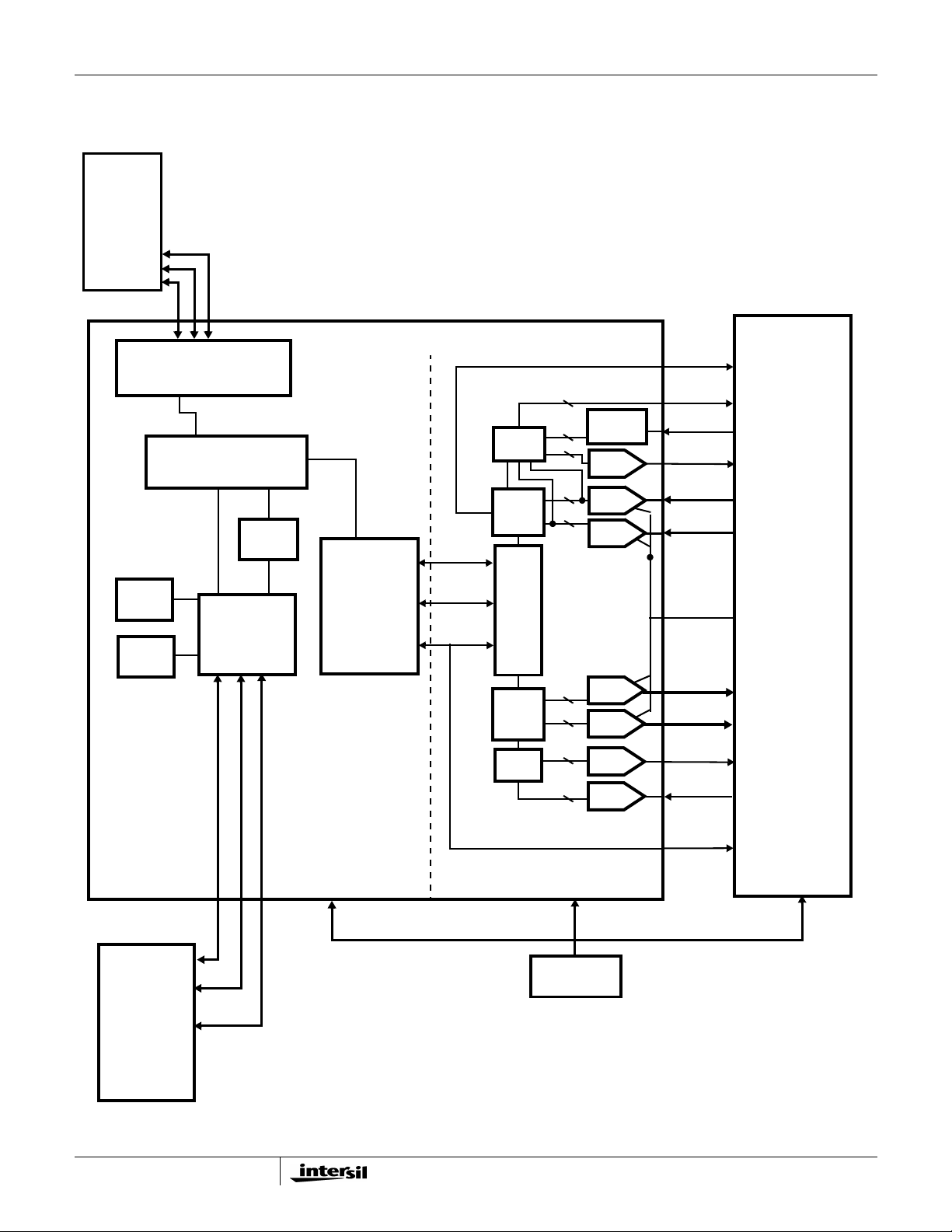
Simplified Block Diagram
HOST
COMPUTER
DATA
ADDRESS
CONTROL
ISL3874
PCI/CARD BUS 32
ON-CHIP
ROM
ON-CHIP
RAM
HOST
INTERFACE
MICRO-
PROGRAMMED
MAC ENGINE
MEMORY
CONTROLLER
WEP
ENGINE
PHY
INTERFACE
(MDI)
SERIAL
CONTROL
(MMI)
ISL3874
DATA I/O
AGC
CTL
DEMOD
I/O
MOD
TX
ALC
1
1
7
6
6
6
6
7
6
THRESH.
DETECT
IF
DAC
I ADC
Q ADC
I DAC
Q DAC
TX
DAC
TX
ADC
ANT_SEL
RX_RF_AGC
RX_IF_DET
RX_IF_AGC
RX_I±
RX_Q±
V
REF
TX_I±
TX_Q±
TX_IF_AGC
TX_AGC_IN
PRISM RADIO
RF SECTION
ADDRESS
DATA
SELECT
EXTERNAL
SRAM AND
FLASH
MEMORY
MEDIUM ACCESS
CONTROLLER
2
BASEBAND PROCESSOR
44MHz CLOCK
SOURCE †
.
RADIO AND SYNTH
SERIAL CONTROL
Page 3

ISL3874
ISL3874 Signal Descriptions
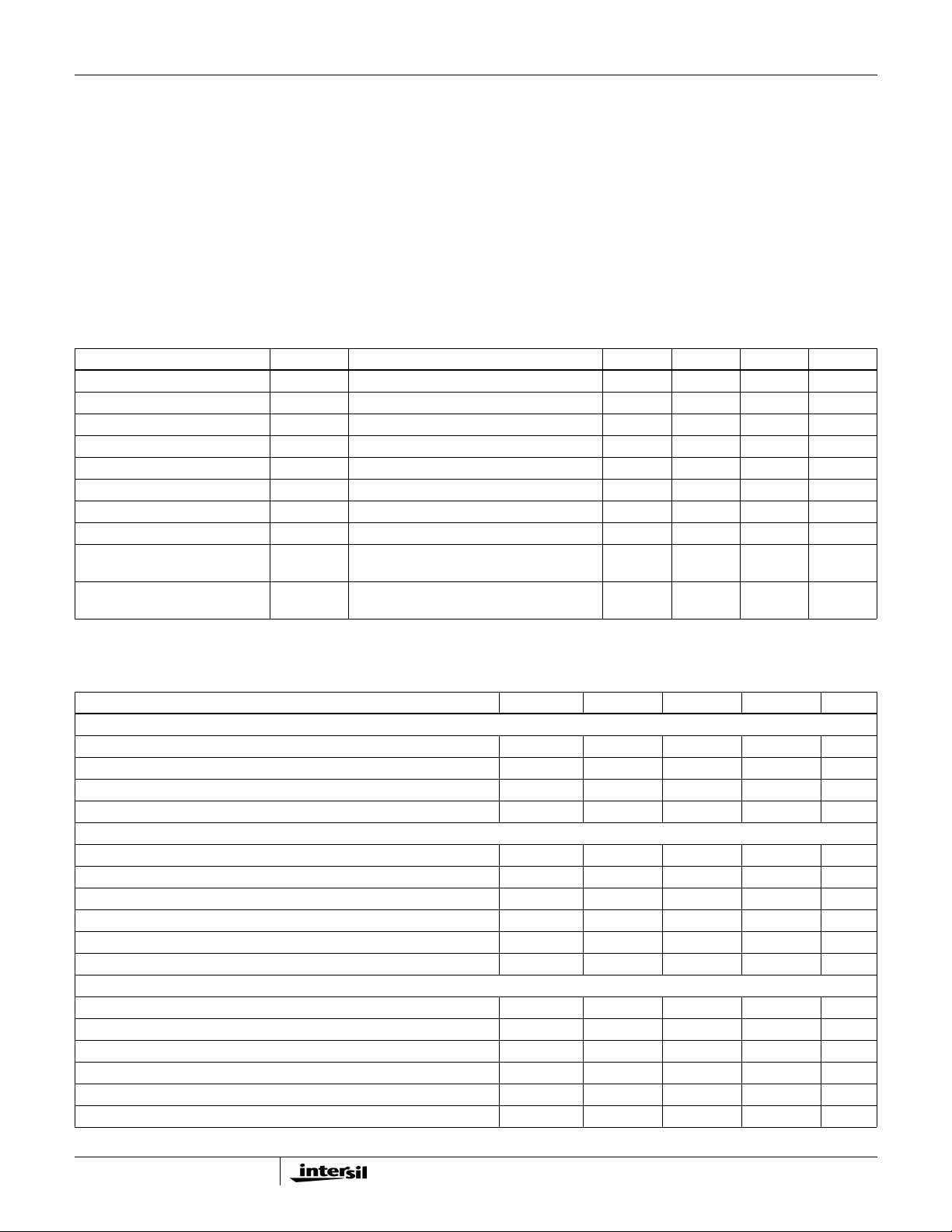
TABLE 1.HOST INTERFACE PINS
PIN NAME
HAD31 A8 5V Tol, CMOS, BiDir PCI address/data bus bit 31. These signals make up the multiplexed PCI address and data bus on
HAD30 A9 5V Tol, CMOS, BiDir PCI address/data bus bit 30.
HAD29 C8 5V Tol, CMOS, BiDir PCI address/data bus bit 29.
HAD28 A10 5V Tol, CMOS, BiDir PCI address/data bus bit 28.
HAD27 B9 5V Tol, CMOS, BiDir PCI address/data bus bit 27.
HAD26 B10 5V Tol, CMOS, BiDir PCI address/data bus bit 26.
HAD25 C9 5V Tol, CMOS, BiDir PCI address/data bus bit 25.
HAD24 A11 5V Tol, CMOS, BiDir PCI address/data bus bit 24.
HAD23 B11 5V Tol, CMOS, BiDir PCI address/data bus bit 23.
HAD22 B12 5V Tol, CMOS, BiDir PCI address/data bus bit 22.
HAD21 A12 5V Tol, CMOS, BiDir PCI address/data bus bit 21.
HAD20 A13 5V Tol, CMOS, BiDir PCI address/data bus bit 20.
HAD19 C12 5V Tol, CMOS, BiDir PCI address/data bus bit 19.
HAD18 A14 5V Tol, CMOS, BiDir PCI address/data bus bit 18.
HAD17 C13 5V Tol, CMOS, BiDir PCI address/data bus bit 17.
HAD16 C14 5V Tol, CMOS, BiDir PCI address/data bus bit 16.
HAD15 E14 5V Tol, CMOS, BiDir PCI address/data bus bit 15.
HAD14 E15 5V Tol, CMOS, BiDir PCI address/data bus bit 14.
HAD13 F16 5V Tol, CMOS, BiDir PCI address/data bus bit 13.
HAD12 F15 5V Tol, CMOS, BiDir PCI address/data bus bit 12.
HAD11 F14 5V Tol, CMOS, BiDir PCI address/data bus bit 11.
HAD10 G16 5V Tol, CMOS, BiDir PCI address/data bus bit 10.
HAD9 G15 5V Tol, CMOS, BiDir PCI address/data bus bit 9.
HAD8 G14 5V Tol, CMOS, BiDir PCI address/data bus bit 8.
HAD7 H15 5V Tol, CMOS, BiDir PCI address/data bus bit 7.
HAD6 G13 5V Tol, CMOS, BiDir PCI address/data bus bit 6.
HAD5 J15 5V Tol, CMOS, BiDir PCI address/data bus bit 5.
HAD4 J14 5V Tol, CMOS, BiDir PCI address/data bus bit 4.
HAD3 K14 5V Tol, CMOS, BiDir PCI address/data bus bit 3.
HAD2 K15 5V Tol, CMOS, BiDir PCI address/data bus bit 2.
HAD1 L14 5V Tol, CMOS, BiDir PCI address/data bus bit 1.
HAD0 L16 5V Tol, CMOS, BiDir PCI address/data bus bit 0.
HBE3 C10 5V Tol, CMOS, BiDir PCI bus commands and byte enables. These signals are multiplexed on the same PCI terminals.
HBE2 B14 5V Tol, CMOS, BiDir PCI bus commands and byte enables. HBE2 applies to byte 2 (HAD23-HAD16).
HBE1 E16 5V Tol, CMOS, BiDir PCI bus commands and byte enables. HBE1 applies to byte 1 (HAD15-HAD8).
PIN
NUMBER PIN I/O TYPE DESCRIPTION
the primary interface. During the address phase of a primary bus PCI cycle, HAD31-HAD0 contain a
32-bit address or other destination information. During the data phase, HAD31-HAD0 contain data.
During the address phase of a primary bus PCI cycle, HBE3-HBE0 define the bus command. During
the data phase, this 4-bit bus is used as byte enables. The byte enables determine which byte paths
of the full 32-bit data bus carry meaningful data. HBE3 applies to byte 3 (HAD31-HAD24).
3
Page 4

ISL3874
TABLE 1.HOST INTERFACE PINS (Continued)
PIN
PIN NAME
HBE0 H16 5V Tol, CMOS, BiDir PCI bus commands and byte enables. HBE0 applies to byte 0 (HAD7-HAD0).
HINTA C6 CMOS, Output PCI Bus Interrupt A
HRESET D6 5V Tol, CMOS, Input PCI reset.
HFRAME B15 5V Tol, BiDir PCI cycle frame. FRAME is driven by the initiator of a bus cycle. FRAME is asserted to indicate
HIRDY A15 5V Tol, CMOS, BiDir PCI initiator ready. HIRDY indicates the PCI bus initiators ability to complete the current data phase
HTRDY A16 5V Tol, CMOS, BiDir PCI target ready. HTRDY indicates the primary bus targets ability to complete the current data
HREQ B7 CMOS, Output PCI bus request. HREQ is asserted by the ISL3874 to request access to the PCI bus as an initiator.
HSERR B16 CMOS, Output PCI system error. HSERR is an output that is pulsed from the ISL3874 when enabled through the
HSTOP C16 5V Tol, CMOS, BiDir PCI cycle stop signal. HSTOP is driven by a PCI target to request the initiator to stop the current
HDEVSEL D15 5V Tol, CMOS, BiDir PCI device select. The ISL3874 asserts HDEVSEL to claim a PCI cycle as the target device. As a
HPERR D16 5V Tol, CMOS, BiDir PCI bus parity. In all PCI bus read and write cycles, the ISL3874 calculates even parity across the
HGNT C7 5V Tol, CMOS, ST
HPCLK A7 5V Tol, CMOS,
HPAR B13 5V Tol, CMOS, BiDir PCI bus parity.
HIDSEL C11 5V Tol, CMOS,
HPME B8 CMOS, Output Power Management Event Output. HPME provides output for PME signals.
NUMBER PIN I/O TYPE DESCRIPTION
that a bus transaction is beginning, and data transfers continue while this signal is asserted. When
FRAME is deasserted, the PCI bus transaction is in the final data phase.
of the transaction. A data phase is completed on a rising edge of PCLK where both HIRDY and
HTRDY are asserted. Until HIRDY and HTRDY are both sampled asserted, wait states are inserted.
phase of the transaction. A data phase is completed on a rising edge of PCLK when both HIRDY
and HTRDY are asserted. Until both HIRDY and HTRDY are asserted, wait states are inserted.
command register indicating a system error has occurred. The ISL3874 need not be the target of
the PCI cycle to assert this signal. When HSERR is enabled in the control register, this signal also
pulses, indicating that an address parity error has occurred on a CardBus interface.
PCI bus transaction. HSTOP is used for target disconnects and is commonly asserted by target
devices that do not support burst data transfers.
PCI initiator on the bus, the ISL3874 monitors HDEVSEL until a target responds. If no target
responds before timeout occurs, the ISL3874 terminates the cycle with an initiator abort.
HD31-HAD0 and BE3-BE0 buses. As an initiator during PCI cycles, the ISL3874 outputs this parity
indicator with a one-PCLK delay. As a target during PCI cycles, the calculated parity is compared
to the initiator parity indicator. A compare error results in the assertion of a parity error (PERR).
PCI bus grant. HGNT is driven by the PCI bus arbiter to grant the ISL3874 access to the PCI bus
Input
Input
Input
after the current data transaction has completed. HGNT may or may not follow a PCI bus request,
depending on the PCI bus parking algorithm.
HPCLK provides timing for all transactions on the PCI bus. All PCI signals are sampled at the rising
edge of PCLK.
Initialization device select. HIDSEL selects the ISL3874 during configuration space accesses.
HIDSEL can be connected to one of the upper 24 PCI address lines on the PCI bus.
4
Page 5

ISL3874
TABLE 2.MEMORY INTERFACE PINS
PIN NAME PIN NUMBER PIN I/O TYPE DESCRIPTION
PL4-MA19 A4 CMOS BiDir, 2mA MBUS Address Bit 19, needed to address between 512KB and 1MB
of data store
MA18 A3 CMOS BiDir, 2mA MBUS Address Bit 18
MA17 B4 CMOS BiDir, 2mA MBUS Address Bit 17
MA16 C3 CMOS TS Output, 2mA MBUS Address Bit 16
MA15 B3 CMOS TS Output, 2mA MBUS Address Bit 15
MA14 A1 CMOS TS Output, 2mA MBUS Address Bit 14
MA13 C2 CMOS TS Output, 2mA MBUS Address Bit 13
MA12 E3 CMOS TS Output, 2mA MBUS Address Bit 12
MA11 B1 CMOS TS Output, 2mA MBUS Address Bit 11
MA10 D2 CMOS TS Output, 2mA MBUS Address Bit 10
MA9 D3 CMOS TS Output, 2mA MBUS Address Bit 9
MA8 C1 CMOS TS Output, 2mA MBUS Address Bit 8
MA7 F4 CMOS TS Output, 2mA MBUS Address Bit 7
MA6 E2 CMOS TS Output, 2mA MBUS Address Bit 6
MA5 D1 CMOS TS Output, 2mA MBUS Address Bit 5
MA4 F2 CMOS TS Output, 2mA MBUS Address Bit 4
MA3 E1 CMOS TS Output, 2mA MBUS Address Bit 3
MA2 F3 CMOS TS Output, 2mA MBUS Address Bit 2
MA1 F1 CMOS TS Output, 2mA MBUS Address Bit 1
MA0 / MWEH- G2 CMOS TS Output, 2mA, 50K Pull Up MBUS Write Enable, high byte. Asserted on writes to the high-order
byte of x16 memory devices that use the JEDEC 4-wire control
interface. Also asserted (as MA[0]) when accessing the odd (high-
order) byte of a word stored in a x8 memory device. During word
accesses of x8 memory, the odd byte is accessed first.
MD15 H4 CMOS, BiDir, 2mA, 50K Pull Up MBUS Data Bit 15
MD14 G1 CMOS, BiDir, 2mA, 50K Pull Up MBUS Data Bit 14
MD13 H3 CMOS, BiDir, 2mA, 50K Pull Down MBUS Data Bit 13
MD12 H2 CMOS, BiDir, 2mA, 50K Pull Down MBUS Data Bit 12
MD11 H1 CMOS, BiDir, 2mA, 50K Pull Up MBUS Data Bit 11
MD10 J3 CMOS, BiDir, 2mA, 50K Pull Up MBUS Data Bit 10
MD9 M1 CMOS, BiDir, 2mA, 50K Pull Up MBUS Data Bit 9
MD8 M3 CMOS, BiDir, 2mA, 50K Pull Down MBUS Data Bit 8
MD7 M2 CMOS, BiDir, 2mA 50K Pull Down MBUS Data Bit 7
MD6 N1 CMOS, BiDir, 2mA, 50K Pull Down MBUS Data Bit 6
MD5 N3 CMOS, BiDir, 2mA, 50K Pull Down MBUS Data Bit 5
MD4 P1 CMOS, BiDir, 2mA, 50K Pull Down MBUS Data Bit 4
MD3 N2 CMOS, BiDir, 2mA, 50K Pull Down MBUS Data Bit 3
MD2 P3 CMOS, BiDir, 2mA, 50K Pull Down MBUS Data Bit 2
MD1 R1 CMOS, BiDir, 2mA, 50K Pull Down MBUS Data Bit 1
MD0 P2 CMOS, BiDir, 2mA, 50K Pull Down MBUS Data Bit 0
5
Page 6
ISL3874
TABLE 2.MEMORY INTERFACE PINS (Continued)
PIN NAME PIN NUMBER PIN I/O TYPE DESCRIPTION
MLBE L3 CMOS BiDir Output, 2mA, 50K Pull Up MBUS Lower Byte Enable. Asserted when accessing the low-order
byte of x16 memory devices that use the JEDEC 5-wire control
interface.
MOE L1 CMOS TS Output, 2mA, 50K Pull Up Memory Output Enable; asserted on memory reads
MWE/ MWEL L2 CMOS TS Output, 2mA, 50K Pull Up Low (or only) Byte Memory Write Enable. Asserted on writes to x8
RAMCS K2 CMOS TS Output, 2mA, 50K Pull Up RAM Select; asserted on MBUS cycles when the address is in the
NVCS K1 CMOS TS Output, 2mA, 50K Pull Up NV Memory Select; asserted on MBUS cycles when the address is in
TABLE 3.GENERAL PURPOSE PORT PINS
PIN NAME PIN NUMBER PIN I/O TYPE
PJ4 T2 CMOS BiDir, 2mA, 50K Pull Down PE1. PE1 and PE2 are bit-encoded functions that
PJ5 T4 CMOS BiDir, 2mA, 50K Pull Down LE_IF. LE_IF and LE_RF are the corresponding serial
PJ6 P4 CMOS BiDir, 2mA LED1.
memory devices, x16 memory devices that use the JEDEC 5-wire
control inteface, or writes to the low-order byte of x16 memory
devices that use the JEDEC 4-wire control interface.
area configured as RAM
the area configured as non-volitile memory.
DESCRIPTION OF FUNCTION
(IF OTHER THAN IO PORT)
control the RF and IF sections.
enables for the IF and RF chips. The trailing edge of the
latch enables (LE) are required to latch the data in the
input register. The last 20 bits of data before the trailing
edge of enables are latched in.
PJ7 T3 CMOS BiDir, 2mA, 50K Pull Down RADIO_PE. This signal is the power enable to the RF
and IF components, but not the baseband.
PK0 R5 CMOS BiDir, 2mA, ST, 50K Pull Down LE_RF. LE_RF and LE_IF are the corresponding serial
PK1 R4 CMOS BiDir, 2mA, 50K Pull Down SYNTHCLK. Separate signals, SYNTHCLK and
PK2 N7 CMOS BiDir, 2mA, 50K Pull Down SYNTHDATA. Separate signals, SYNTHDATA and
PK3 R6 CMOS BiDir, 2mA, 50K Pull Down PA_PE. This signal, when asserted high, enables the
PK4 T5 CMOS BiDir, 2mA, 50K Pull Down PE2. PE2 and PE1 are bit-encoded functions that
PK7 P7 CMOS BiDir, 2mA, 50K Pull Down CAL_EN. Calibrates the Rx function to eliminate DC
PL3 P8 CMOS BiDir, 2mA, 50K Pull Up TR_SW_BAR. Antenna Diversity Control
PL7 T6 CMOS BiDir, 2mA, 50K Pull Down TR_SW. Antenna Diversity Control
enables for the RF and IF chips. The trailing edge of the
latch enables (LE) are required to latch the data in the
input register. The last 20 bits of data before the trailing
edge of enable are latched in.
SYNTHDATA, are used to program the synthesizer
through bit manipulation in firmware.
SYNTHCLK, are used to program the synthesizer
through bit manipulation in firmware.
Tx section of the Modulator/Demodulator and RF/IF
up/down converter circuits.
control the RF and IF sictions.
offset in the Rx chain.
6
Page 7
ISL3874
TABLE 4.SERIAL EEPROM PORT CONNECTIONS
PIN NAME PIN NUMBER PIN I/O TYPE DESCRIPTION
PJ0 P5 CMOS BiDir, 2mA, 50K Pull Up SCLK, serial clock for serial EEPROM devices
PJ1 T1 CMOS BiDir, 2mA, 50K Pull Down Serial Data Out (SD) used on serial EEPROM devices which require
three and four wire interfaces, example: AT45DB011
PJ2 R3 CMOS BiDir, 2mA, 50K Pull Down Serial Data In (MISO) used on serial EEPROM devices, Used in four wire
serial devices only. Not currently supported in software. Consult the
factory for additional updates on this option.
TCLKIN(CS) L4 I/O, 50K Pull Down CS used for Chip Select Output for Serial Devices which have a 4 wire
interface like the AST45DB011 and also serial data on two wire devices
like the 24C08.
TABLE 5.CLOCKS PORT PINS
PIN NAME PIN NUMBER PIN I/O TYPE DESCRIPTION
XTALIN J2 Analog Input 32.768kHz Crystal Input
XTALOUT J1 CMOS Output, 2mA 32.768kHz Crystal Output
CLKOUT A2 CMOS, TS Output, 2mA Clock Output (Selectable as MCLK, TCLK, or TOUT0)
BBP_CLK J16 Input Baseband Processor Clock. The nominal frequency for this clock is 44 MHz.
TABLE 6.BASEBAND PROCESSOR RECEIVER PORT PINS
PIN NAME PIN NUMBER PIN I/O TYPE DESCRIPTION
RX_IF_AGC T16 O Analog drive to the IF AGC control.
RX_RF_AGC P16 O Drive to the RF AGC stage attenuator. CMOS digital.
RX_IF_DET R10 I Analog input to the receive power A/D converter for AGC control.
RXI+ R7 I Analog input to the internal 6-bit A/D of the In-phase received data. Balanced differential.
RXI- T7 I Analog input to the internal 6-bit A/D of the In-phase received data. Balanced differential.
RXQ+ R9 I Analog input to the internal 6-bit A/D of the Quadrature received data. Balanced differential.
RXQ- T9 I Analog input to the internal 6-bit A/D of the Quadrature received data. Balanced differential.
TABLE 7.BASEBAND PROCESSOR TRANSMITTER PORT PINS
PIN NAME PIN NUMBER PIN I/O TYPE DESCRIPTION
TX_AGC_IN T10 I Input to the transmit power A/D converter for transmit AGC control.
TX_IF_AGC R16 O Analog drive to the transmit IF power control.
TXI+ R12 O TX Spread baseband I digital output data. Data is output at the chip rate. Balanced differential.
TXI− T12 O TX Spread baseband I digital output data. Data is output at the chip rate. Balanced differentia.
TXQ+ R14 O TX Spread baseband Q digital output data. Data is output at the chip rate. Balanced differential.
TXQ− T14 O TX Spread baseband Q digital output data. Data is output at the chip rate. Balanced differential.
7
Page 8
ISL3874
TABLE 8.MISCELLANEOUS CONTROL PORT PINS
PIN NAME PIN NUMBER PIN I/O TYPE DESCRIPTION
GRESET L15 I Global Reset for MAC, Active LOW
TCLKIN(CS) L4 I/O, 50K Pull
Down
ANTSEL N15 O The antenna select signal changes state as the receiver switches from antenna to antenna during
ANTSEL N16 O The antenna select signal changes state as the receiver switches from antenna to antenna during
Test_Mode C4 I Must be tied to GND.
CompCap1 R15 I Compensation Capacitor.
CompCap2 R13 I Compensation Capacitor.
CompRes1 T15 I Compensation Resistor.
CompRes2 P13 I Compensation Resistor.
DBG4
(MPCIACT)
DBG3
(CLKRUN)
DBG2
(LED2)
DBG1 B5 I/O Manufacturing Debug Signals, Leave Unconnected.
DBG0 A6 I/O Manufacturing Debug Signals, Leave Unconnected.
B6 I/O Manufacturing Debug Signals, Leave Unconnected.
A5 I/O Manufacturing Debug Signals, Leave Unconnected.
C5 I/O Manufacturing Debug Signals, Leave Unconnected.
CS used for Chip Select Output for Serial Devices which have a 4 wire interface like the
AST45DB011 and also serial data on two wire devices like the 24C08.
the acquisition process in the antenna diversity mode. This is a complement for ANTSEL (pin 40) for
differential drive of antenna switches.
the acquisition process in the antenna diversity mode. This is a complement for ANTSEL (pin 39) for
differential drive of antenna switches.
Connected to MPCIACT Signal on Mini-PCI Connector.
Connected to CLKRUN Signal on Mini-PCI Connector.
Used as LED2 Output Signal.
TABLE 9.POWER PORT PINS
PIN NAME PIN NUMBER PIN I/O TYPE DESCRIPTION
V
DDA
V
DD
V
SSA
V
sub
GND B2, D5, D8, D10, D12, D13,
V
REF
I
REF
NC P15, P14, N11, M14, C15, L13,
ST = Schmitt Trigger (Hysteresis), TS = Three-State. Signals ending with “-” are active low.
M13, P12, R11, T8, R8, P9 Power Analog DC Power Supply 2.7 - 3.6V.
P6, D4, D7, D9, D11, D14, F13,
H13, K16, M15, N5, N4, K4,
G3, E4
N13, T13, T11, N9 GND Analog Ground.
N10, P10 GND Analog Ground.
E13, H14, J13, N14, N8, N6,
R2, M4, K3, J4, G4
P11 Input Voltage Reference for A/Ds and D/As.
N12 Input Current Reference for internal ADC and DAC devices. Requires 12K resistor to
M16, K13
Power Digital DC Power Supply 2.7 - 3.6V.
GND Digital Ground.
ground.
NC No Connection.
8
Page 9
ISL3874
Absolute Maximum Ratings Thermal Information
Supply Voltage. . . . . . . . . . . . . . . . . . . . . . . . . . . . . . . . . . . . . . . 4V
Input, Output or I/O Voltage. . . . . . . . . . . GND -0.5V to V
ESD Classification . . . . . . . . . . . . . . . . . . . . . . . . . . . . . . . . Class 2
CC
+0.5V
Operating Conditions
Voltage Range. . . . . . . . . . . . . . . . . . . . . . . . . . . . . . . . . . . . . +3.3V
Ambient Temperature Range. . . . . . . . . . . . . . . . . . . -40oC to 85oC
CAUTION: Stresses above those listed in “Absolute Maximum Ratings” may cause permanent damage to the device. This is a stress only rating and operation of the
device at these or any other conditions above those indicated in the operational sections of this specification is not implied.
1. θJA is measured with the component mounted on a low effective thermal conductivity test board in free air. See Tech Brief TB379 for details.
Thermal Resistance (Typical, Note 1) θJA (oC/W)
BGA Package. . . . . . . . . . . . . . . . . . . . . . . . . . . . . . 56
Maximum Storage Temperature Range . . . . . . . . . -65oC to 150oC
Maximum Junction Temperature. . . . . . . . . . . . . . . . . . . . . . .100oC
Maximum Soldering Temperature . . . . . . . . . See Tech Brief TB334
DC Electrical Specifications (Test conditions @ 25
o
C)
PARAMETER SYMBOL TEST CONDITIONS MIN TYP MAX UNITS
Power Supply Current I
Standby Power Supply Current I
CCOP
CCSB
Input Leakage Current I
Output Leakage Current I
Logical One Input Voltage V
Logical Zero Input Voltage V
Logical One Output Voltage V
Logical Zero Output Voltage V
Input Capacitance C
OH
OL
VCC = 3.6V, CLK Frequency = 44MHz - 170 TBD mA
VCC = Max, Outputs Not Loaded - 3 TBD mA
VCC = Max, Input = 0V or V
I
VCC = Max, Input = 0V or V
O
VCC = Max, Min 0.7V
IH
VCC = Min, Max - - VCC*0.3 V
IL
CC
CC
- 100 TBD nA
- 300 TBD nA
CC
IOH = -1mA, VCC = Min VCC-0.2 2.6 - V
IOL = 2mA, VCC = Min - 0.05 0.2 V
CLK Frequency = 1MHz. All measurements
IN
- 5 10 pF
referenced to GND. TA = 25oC
Output Capacitance C
OUT
CLK Frequency 1MHz. All measurements
- 5 10 pF
referenced to GND. TA = 25oC
NOTE:All values in this table have not been measured and are only estimates of the performance at this time.
AC Electrical Specifications
PARAMETER SYMBOL MIN TYP MAX UNITS
CLOCK SIGNAL TIMING
OSC Clock Period (Typ. 44MHz) t
High Period t
Low Period t
Full Scale Input Voltage (V
) TBD TBD 4 V
P-P
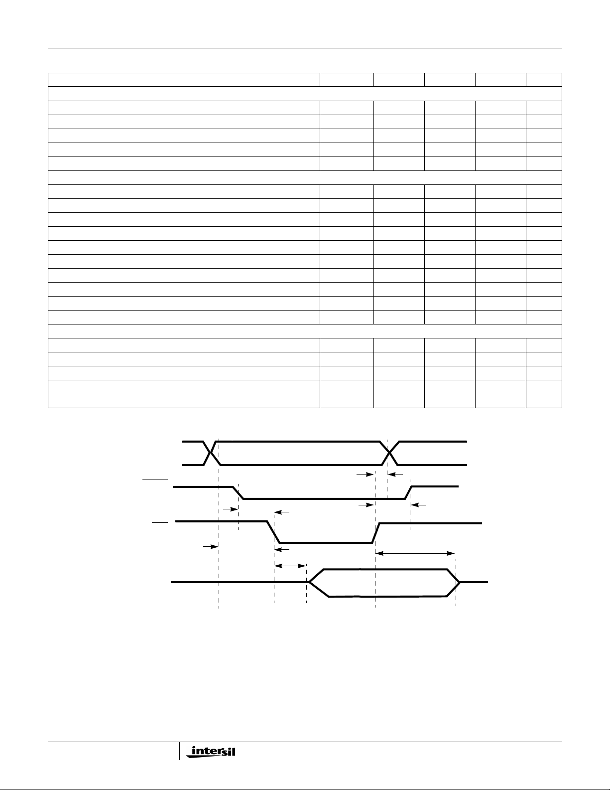
EXTERNAL MEMORY READ INTERFACE
MOE-Setup Time from RAMCS_ t
MOE_Setup Time from MA (17..0) t
MA (17..1) Hold Time from MOE_ Rising Edge t
RAMCS_ Hold from MOE_ Rising Edge t
MD (15..0) Enable from MOE_ Falling t
MO (15..0) Disable from MOE_ Rising Edge t
EXTERNAL MEMORY WRITE INTERFACE
MA (17..0) Setup to MWE_ Falling Edge t
RAMCS_ Setup to MWE t
MA (17..0) Hold from MWE_ Rising Edge t
RAMCS _ Hold from MWE_ Rising Edge t
MD (15..0) Setup to MWE_ Rising Edge t
MD (15..0) Hold from MWE_ Rising Edge t
CYC
H1
L1
S1
S2
H1
H2
E1
D1
S3
S4
H3
H4
S5
H5
22.5 20.8 200 ns
10 10.4 - ns
10 10.4 - ns
0 - - ns
0
20 - - ns
20 - - ns
5
-
0 0 0 ns
0 - - ns
15 - - ns
15 - - ns
40 - - ns
15 - - ns
- - V
-
-
-
- ns
- ns
100 ns
9
Page 10
ISL3874
AC Electrical Specifications (Continued)
PARAMETER SYMBOL MIN TYP MAX UNITS
SYNTHESIZER
SYNTHCLK(PK1) Period t
SYNTHCLK(PK1) Width Hi t
SYNTHCLK(PK1) Width Lo t
SYNTHDATA(PK2) Hold Time from Falling Edge of SYNTHCLK(PK1) t
SYNTHCLK(PK1) Falling Edge to SYNLE Inactive t
CYC
H1
L1
D2
D3
SYSTEM INTERFACE - PCI TIMING
Cycle Time, HPCLK t
Pulse Duration, HPCLK High t
Pulse Duration, HPCLK Low t
Slew Rate, HPCLK t
Propagation Delay Time, HPCLK to Signal Valid Delay Time t
Propogation Delay Time, HPCLK to Signal Invalid Delay Time t
Enable Time, High Impedance to Active Delay Time from HPCLK t
Disable Time, Active to High Impedance Delay Time from HPCLK t
Setup Time Before HPCLK Valid t
Hold Time After HPCLK High t
CYC
H
L
S
V
INV
EN
DIS
S
H
BASEBAND SIGNALS
Full Scale Input Voltage (V
) 0.25 0.50 1.0 V
P-P
Input Bandwidth (-0.5dB) - 20 - MHz
Input Capacitance - 5 - pF
Input Impedance (DC) 5 - - kΩ
FS (Sampling Frequency) - - 22 MHz
90 - 4,000 ns
t
/2 - 10 - t
CYC
t
/2 - 10 - t
CYC
/2 + 10 ns
CYC
/2 + 10 ns
CYC
0 - - ns
35 - - ns
30 - - ns
11 - - ns
11 - - ns
1 - 4 V/ns
- - 11 ns
2 - - ns
2 - - ns
- - 28 ns
7 - - ns
0 - - ns
Waveforms
ADDRESS
MA(17..1)
RAMCS
MOE
MD(15..0)
t
H1
t
S1
t
S2
t
E1
FIGURE 1.MAC EXTERNAL MEMORY READ TIMING
t
H2
t
D1
10
Page 11

Waveforms (Continued)
ADDRESS
MA(17..1)
RAMCS
MWE
MD(15..0)
ISL3874
t
H3
t
S4
t
S3
t
S5
FIGURE 2.MAC EXTERNAL MEMORY WRITE TIMING
t
H4
t
H5
HPCLK
PCI OUTPUT
SYNTHCLK
SYNLE
SPCSPWR
SYNTHDATA
1.5V
tH1t
L1
t
CYC
t
D1
D[n] D[n -1] D[n -2] D[2] D[1] D[0]
t
D2
FIGURE 3.SYNTHESIZER
t
H
t
L
t
CYC
FIGURE 4.HPCLK TIMING WAVEFORM
t
V
VALID
t
INV
t
D3
PCI INPUT
11
t
EN
VALID
t
S
t
H
FIGURE 5.PCI BUS TIMING WAVEFORMS
t
DIS
Page 12

ISL3874
ISL3874
MA0/MWEH
MD0..15
MA1..17
NVCS
MOE
MWEL
RAMCS
SRAM
128Kx8
MD0..7
MA1..17
OE
WE
CS
FIGURE 6.8 BIT MEMORY INTERFACE
FLASH
128Kx8
MD0..7
MA0..16
CS
OE
WE
SRAM
128Kx8
MD8..15
MA1..17
OE
WE
CS
ISL3874
MA0/MWEH
MA1..17
MD0..15
NVCS
MLBE
RAMCS
MOE
MWEL
FLASH
128Kx16
ADDR(0..16)
DATA(0..15)
CE
OE
WE
SRAM
128Kx16
ADDR(0..16)
DATA(0..15)
UB
LB
CE
OE
WE
FIGURE 7.16-BIT MEMORY INTERFACE
12
Page 13

ISL3874
LARGE SERIAL EEPROM
MISO (PJ2)
SD (PJ1)
ISL3874
SCLK (PJ0)
CS# (TCLKIN)
PULLUP
SI
SCK
CS
AT45DB011
FIGURE 8.SERIAL EEPROM MEMORY INTERFACE
SO
PULLUP
RESET#
WP#
External Memory Interface
The ISL3874 provides separate external chip selects for
code space and data storage space. Code space is
accessible as data space through an overlay mechanism,
except for an internal ROM. Refer to Figures 6 , 7 and 8 for
ISL3874 memory configuration detail examples.
The maximum possible memory space size is 4Mbytes.
Most of the data store space is reserved for storage of
received and transmitted data, with some areas reserved for
use by firmware. However, a portion of the data store may
be allocated as code store. This permits higher speed
instruction execution, by using fast RAMs, than is possible
from Flash memories. The maximum size of this overlay is
the full code space address range, 128kbytes, and is
allocated in independent sections of 16KBytes each, on
16kbyte boundaries, ranging from the highest address of the
actual physical memory space and extending down.
SMALL SERIAL DEVICES
PULLUP
AO
ISL3874
CS# (TCLKIN)
SCLK (PJ0)
SDA
SCL
(NOTE:MUST OPERATE
A1
A2
WP
24C08
AT 400kHz AT 3.3VDC)
The external SRAM memory must be organized in a 16-bit
width to provide adequate performance to implement the
802.11 protocol at 11Mb/s rates. Systems designed for lower
performance applications may be able to use 8-bit wide
memory.
The minimum external memory is 128kbytes of SRAM,
organized 8 or 16 bits wide. Typical applications, including
802.11 station designs, use 256kbytes organized 128K x 16.
An access point application could make use of the full address
space of the device with 4Mbytes organized a 2M x 16.
The ISL3874 supports 8 or 16-bit code space, and 8 or 16-bit
data space. Code space is typically populated with the least
expensive Flash memory available, usually an 8-bit device.
Data space is usually populated with high-speed RAMs
configured as a 16-bit space. This mixing of 8/16 bit spaces is
fully supported, and may be done in any combination desired
for code and data space.
Mapping code execution to RAM requires the RAM to have
code written into it. Typically, this is done by placing code in a
non-volatile memory such as a Flash in the code space. At
initialization, the code in the non-volatile memory transfers itself
to RAM, maps the appropriate blocks of the code space to the
RAM, and then branches to begin execution from RAM. This
allows low cost, slow Flash devices to hold an entire code
image, which can be executed much faster from RAM. If code
is not placed in an external non-volatile memory as described
here, it must be transferred to the RAM via the Host Interface.
Slow memories are not dynamically sensed. Following reset,
the instruction clock operates with a slower cycle while the
Flash is copied to RAM. Once code has been copied from
Flash to RAM, execution transfers to RAM and the clock is
raised to the normal operating frequency.
As mentioned above, it is feasible to operate without a code
image in a non-volatile memory. In such a system, the
firmware must be downloaded to RAM through the host
interface before operation can commence.
13
The ISL3874 supports direct control of single chip 16-bit
wide SRAMs with high/low byte enables, as well as direct
control of a 16-bit space constructed from 8-bit wide SRAMs.
The type of memory configuration is specified via the
appropriate MD pin, sensed when the ISL3874 is reset.
ISL3874 pin MA0/MWEH functions as Address 0 for 8-bit
access, (such as Flash) as MWEH (High Byte Write Enable)
when two x8 memories are configured as a single x16
space, and as the upper Byte Enable when a single x16
memory is used. No external logic is required to generate
the required signals for both types of memory configurations,
even when both exist together; all that is required is for the
ISL3874 code to configure the ISL3874 memory controller to
generate the proper signals for the particular address space
being accessed.
For 8-bit spaces, the ISL3874 dynamically configures pin
MA0/MWEH cycle-by-cycle as the address LSB.
Page 14

ISL3874
MWEL/MWE is the only write control, and MOE is the read
output enable.
For 16-bit spaces constructed from 8-bit memories, the
ISL3874 dynamically configures pin MA0/MWEH cycle-bycycle as the high byte write enable, MWEL as the low write
enable signal, and MOE as the read output enable.
For 16-bit spaces constructed from single-chip x16
memories (such as SRAMs), the ISL3874 dynamically
configures pin MA0/MWEH cycle-by-cycle as the upper byte
enable. Pin MLBE is connected as the low byte enable,
MWEL/MWE is the write control, and MOE is the read output
enable.
These memory implementations require no external logic.
The memory spaces may each be constructed from any type
of memory desired. The only restriction is that a single
memory space must be constructed from the same type of
memory; for example, data space may not use both x8 and
x16 memories, it must be all x8, or all x16. This restriction
does not apply across memory spaces; e.g., code space
may use a x8 memory and data space a single x16 memory,
or code space two x8 memories and data space a single x8
memory.
Serial EEPROM Memory Interface
The ISL3874 contains a small on-ship ROM firmware which
was added to allow the CIS or CIS plus firmware image to be
transferred from a off-chip serial nonvolatile memory device
to RAM after a system reset. This allows a system
configuration without a parallel Flash device. The operating
frequency for the 24C08 Serial EEPROM must be 400kHz
with an operating voltage of 3.3V. Refer to Figure 8 for
additional details on configuring the serial memory to the
ISL3874.
The Power On Reset Configuration Section in this document
provides additional details on memory selection and control
after a reset condition.
PC Card Interface
The PCI Host Interface allows access to the ISL3874
memory and host registers using PCI memory read or write
transactions.
The host interface supports Target Mode operation
transferring double words. Direct memory access to the
ISL3874 memory space using Aux port transfers is
supported in Target Mode. BAP transfers operate in Target
Mode in a similar manner to how they worked on the
HFA3842 and thus allow quick porting of base functionality
HFA3842 driver code to this part.
Most of the host side registers have been preserved except
where functionality is no longer needed. For example, the
attribute FCR registers are not implemented since attribute
space does not exist for the PCI interface. Only memory
space is implemented in this part so PCI I/O read or write
operations are not defined.
PCI Interface Configuration
The PCI core has two sets of configuration registers. One
set is read-only and configured to default values or set up by
ISL3874 firmware on reset. This set is used by the host to
determine what type of card this is, and what drivers need to
be loaded. The other set is the host configuration registers.
These are written by the host to configure various options
and responses of the PCI card.
During reset the core’s strapping options cause one of two
scenarios to occur for loading the read-only PCI
configuration registers. If the part is set to power up and run
then the ISL3874 firmware is responsible for fetching values
from its memory space and loading them into the proper
registers. Note that the interface will be unable to respond to
host commands including configuration commands until
these registers have been loaded.
If the part is set to power up and go idle then default values
are loaded into the read-only registers so that the PCI
interface can be initialized by the host. This mode is most
likely the case when downloading firmware code via the Aux
port. Since there is no existing firmware to control the part
the default values allow the host to configure the rest of the
interface enough to be able to download code into the
memory space of the ISL3874.
The read-only registers set the device id, vendor id, class
code, revision id, header type, subsystem id, subsystem
vendor id, maximum latency, minimum grant, and the
interrupt pin. These registers are all 16 bits wide and are
loaded by the DBus. They must be loaded in the following
order: {max_lat, min_gnt}, {class_code[23:16], header},
class_code[15:0], {int_pin, rev_id}, subsys_id,
subsys_vendor_id, device_id, vendor_id.
The default values are:
• device_id 0x3873
• vendor_id 0x1260 // Intersil PCI SIG vendor id.
• class_code 0x02_8000
• subsys_id 0x0000
• subsys_vendor_id 0x1260 // Intersil PCI SIG vendor id.
• rev_id 0x01
• header 0x00
• max_lat 0x00
• min_gnt 0x00
• int_pin 0x01 // Int A
On reset or power up the PCI interface has several host
configuration registers that must be written by the host
before normal target memory read/write transactions can be
used. Target operations are enabled once the Memory Base
Address and the Command registers have been written.
14
Page 15

ISL3874
These are the minimum set of registers required for the card
to respond to a target operation.
The Memory Base Address register is used to set the starting
address range this device will respond to. The maximum
address space for this chip is 4K. The Command register
enables specific features of the PCI host interface. The
Memory Access Enable bit must be set to allow any read/write
operations. Further information about the PCI configuration
registers can be found in the PCI 2.1 Interface spec.
Target Mode Operation
This mode is the default or base mode of communicating with
the ISL3874 processor. After the host configures the PCI
interface itself, PCI memory read and write transactions are
used to initialize the processor and to send it commands.
These transactions access host side register addresses in
much the same way as the HFA3842 did. Host registers have
had their address DWORD aligned (shifted left by one) from the
register map used by the HFA3842. This allows ordinary
double word accesses to take place on any given host register.
Host register addresses are 8 bits wide and wrap at 0xFF in
memory space up to the maximum address space. Each
register provides up to 16 bits of valid data depending on the
PCI read or write system call request length. PCI requests for
greater than word length (16 bits) will have the upper bits
zeroed.
PCI Specific Implementation
The ISL3874 host side memory space is not intended to be
written in a sequential manner so burst operations are not
supported.
Only memory read, memory write, and configuration cycles
are supported in target mode. Fast block transfers with the
least amount of host overhead can be implemented in
Master mode, however, throughput will be limited by
available Mbus bandwidth. BAP transfers are supported in
Target mode and should be faster than equivalent PCMCIA
BAP transactions. This allows a port of the existing driver
from the PCMCIA part to PCI with minimal changes.
The ISL3874 is a single function device so only one interrupt,
HINTA, is used. An interrupt is generated whenever one of the
interrupt sources in the ISR goes active and the corresponding
bit in the IMR is enabled. The interrupt pin, HINTA, generates
an active low level when requesting an interrupt.
Reset
There are two reset pins for this part. The first, GRESET is a
hardware reset pin used to reset the entire part on power up.
The second reset is the HRESET. This is intended to reset
only the PCI interface section.
A soft reset is available which does not reset any of the PCI
core read-only configuration registers. This soft reset is
accomplished in the same manner as the HFA3842 by
writing a one to COR[7]. Note this register has been moved
from its previous location. It now resides at location 0x4C.
Only bit 7 (Soft Reset) is implemented for this register. The
HCR and COR registers are the only registers that can be
written during soft reset. The HCR can be written to override
the default MBus strapping options and COR[7] is reset to
bring the part out of soft reset.
LOCK# is not implemented. We do not have atomic
accesses and thus have no need to support this. Further, it
is not implemented in the mini-PCI spec.
Normal Operating Modes
Target mode has three different types of accesses. The
biggest difference between them as far as the host is
concerned is the amount of time it takes to complete the
accesses. The three types are hardware registers, memory
mapped registers and BAP data registers.
Hardware registers complete their access in one M clock
cycle, which at normal M clock speeds means the PCI read
will complete without a retry.
Memory mapped read cycles will almost always require at
least one retry depending on M clock speed and how soon
the ISL3874 memory controller grants the memory request.
BAP read cycles can fall into either case depending on
whether or not a preread completes prior to the host
requesting another transfer.
The PCI interface supports one level of posted writes. That
is, the first write cycle will be accepted and the PCI interface
will complete the transaction immediately. If another write
occurs before the first write has completed internally, it will
not be accepted and the PCI bus will have to retry the write
at a later time.
PC Card Physical Interface
The Host interface is compatible to the Mini-PCI
Specification. Further details on programming and
controlling the PCI interface can be found in the
programmers manual for the ISL3874. The following
describes specific features of various pins:
HAD(0-31) - PCI Card Address and Data Input, Bits 0 to 31.
These signals make up the multiplexed PCI address and data
bus on the primary interface. During the address phase of a
primary bus PCI cycle, HAD31-HAD0 contain a 32-bit address
or other destination information. During the data phase,
HAD31-HAD0 contain data.
HBE2 - PCI bus commands and byte enables. HBE2 applies
to byte 2 (HAD23-HAD16).
HBE1 - PCI bus commands and byte enables. HBE1 applies
to byte 1 (HAD15-HAD8).
HBE0 - PCI bus commands and byte enables. HBE0 applies
to byte 0 (HAD7-HAD0).
HIDSEL - Initialization device select. HIDSEL selects the
ISL3874 during configuration space accesses. HIDSEL can
15
Page 16

ISL3874
be connected to one of the upper 24 PCI address lines on
the PCI bus.
HRESET - PCI Card reset signal. This reset signal only
resets the PCI core.
HFRAME - PCI Card FRAME cycle signal. FRAME is driven
by the initiator of a bus cycle. FRAME is asserted to indicate
that a bus transaction is beginning, and data transfers
continue while this signal is asserted. When FRAME is
deasserted, the PCI bus transaction is in the final data
phase.
HIRDY - PCI initiator ready. HIRDY indicates the PCI bus
initiators ability to complete the current data phase of the
transaction. A data phase is completed on a rising edge of
PCLK where both HIRDY and HTRDY are asserted. Until
HIRDY and HTRDY are both sampled asserted, wait states
are inserted.
HPAR - PCI bus parity. The ISL3874 calculates even parity
across the buses HAD(31-0) and HBE(3-0).
HTRDY - PCI target ready. HTRDY indicates the primary bus
targets ability to complete the current data phase of the
transaction. A data phase is completed on a rising edge of
PCLK when both HIRDY and HTRDY are asserted. Until both
HIRDY and HTRDY are asserted, wait states are inserted.
HDEVSEL - PCI device select. The ISL3874 asserts
HDEVSEL to claim a PCI cycle as the target device. As a
PCI initiator on the bus, the ISL3874 monitors HDEVSEL
until a target responds. If no target responds before a
timeout occurs, the ISL3874 terminates the cycle with an
initiator abort.
HSTOP - PCI cycle stop signal. HSTOP is driven by a PCI
target to request the initiator to stop the current PCI bus
transaction. HSTOP is used for target disconnects and is
commonly asserted by target devices that do not support
burst data transfers.
HPERR - PCI parity error indicator. HPERR is driven by a
PCI device to indicate that the calculated parity does not
match HPAR when HPERR is enabled.
HSERR - PCI system error. HSERR is an output that is
pulsed from the ISL3874 when enabled through the
command register indicating a system error has occurred.
The ISL3874 need not be the target of the PCI cycle to
assert this signal. When HSERR is enabled in the control
register, this signal also pulses, indicating that an address
parity error has occurred on a CardBus interface.
HREQ - PCI bus request. HREQ is asserted by the ISL3874
to request access to the PCI bus as an initiator.
HGNT - PCI bus grant. HGNT is driven by the PCI bus
arbiter to grant the ISL3874 access to the PCI bus after the
current data transaction has completed. HGNT may or may
not follow a PCI bus request, depending on the PCI bus
parking algorithm.
HPCLK - HPCLK provides timing for all transactions on the
PCI bus. All PCI signals are sampled at the rising edge of
PCLK.
HPME - Power Management Event Output. HPME provides
output for PME signals.
Register Interface
The logical view of the ISL3874 from the host is a block of 32
word wide registers. These appear in IO space starting at
the base address determined by the socket controller. There
are three types of registers.
HARDWARE REGISTERS (HW)
• 1 to 1 correspondence between addresses and registers.
• No memory arbitration delay, data transfer directly to/from
registers.
• AUX base and offset are write-only, to set up access
through AUX data port.
• Note: All register cycles, including hardware registers,
incur a short wait state on the PC Card bus to insure the
host cycle is synchronized with the ISL3874’s internal
MCLK.
MEMORY MAPPED REGISTERS IN DATA RAM (MM)
• 1 to 1 correspondence.
• Requires memory arbitration, since registers are actually
locations in ISL3874 memory.
• Attribute memory access is mapped into RAM as Baseaddress + 0x400.
• AUX port provides host access to any location in ISL3874
RAM (reserved).
BUFFER ACCESS PATH (BAP)
• No 1 to 1 correspondence between register address and
memory address (due to indirect access through buffer
address pointer registers).
• Auto increment of pointer registers after each access.
• Require memory arbitration since buffers are located in
ISL3874 memory.
• Buffer access may incur additional delay for Hardware
Buffer Chaining.
Buffer Access Paths
The ISL3874 has two independent buffer access paths,
which permits concurrent read and write transfers. The
firmware provides dynamic memory allocation between
Transmit and Receive, allowing efficient memory utilization.
On-the-fly allocation of (128-byte) memory blocks as needed
for reception wastes minimal space when receiving
fragments. The ISL3874 hides management of free memory
from the driver, and allows fast response and minimum data
copying for low latency. The firmware provides direct access
to TX and RX buffers based on Frame ID (FID). This
16
Page 17

ISL3874
facilitates Power Management queuing, and allows dynamic
fragmentation and defragmentation by controller. Simple
Allocate/Deallocate commands insure low host CPU
overhead for memory management.
Hardware buffer chaining provides high performance while
reading and writing buffers. Data is transferred between the
host driver and the ISL3874 by writing or reading a single
register location (The Buffer Access Path, or BAP). Each
access increments the address in the buffer memory.
Internally, the firmware allocates blocks of memory as needed
to provide the requested buffer size. These blocks may not be
contiguous, but the firmware builds a linked list of pointers
between them. When the host driver is transferring data
through a buffer access path and reaches the end of a
physical memory block, hardware in the host interface follows
the linked list so that the buffer access path points to the
beginning of the next memory block. This process is
completely transparent to the host driver, which simply writes
or reads all buffer data to the same register. If the host driver
attempts to access beyond the end of the allocated buffer,
subsequent writes are ignored, and reads will be undefined.
Power Sequencing
The ISL3874 provides a number of firmware controlled port
pins that are used for controlling the power sequencing and
other functions in the front end components of the radio.
Packet transmission requires precise control of the radio.
Ideally, energy at the antenna ceases after the last symbol of
information has been transmitted. Additionally, the
transmit/receive switch must be controlled properly to protect
the receiver. It is also important to apply appropriate
modulation to the PA while it's active.
Signaling sequences for the beginning and end of normal
transmissions are illustrated in Figure 9. Table 10 lists
applicable delays associated with these control signals.
A transmission begins with PE2 as shown in Figure 9. Next,
the transmit/receive switch is configured for transmission via
the differential pair TR_SW and TR_SW_BAR. This is
followed by a transmit enable (TX_ENABLE) to the
Baseband processor inside the ISL3874. This enable
activates the transmit state machine in the BBP. Lastly,
PA_PE activates the PA. Delays for these signals related to
the initiation of transmission are referenced to PE2.
Immediately after the final data bit has been clocked out of the
MAC the Baseband processor is disabled. The MAC in then
waits for a control signal (TX_READY) from the Baseband
processor to go inactive, signaling that the BBP has modulated
the final information-rich symbol. It then immediately de-asserts
PA_PE followed by placing the transmit/receive switch in the
receive position and ending with PE2 going high. Delays for
these signals related to the termination of transmission are
referenced to the rising edge of PE2.
TABLE 10.TRANSMIT CONTROL TIMING SPECIFICATIONS
PARAMETER SYMBOL DELAY TOLERANCE UNITS
TX_PE to PE2 t
TX_PE to PA_PE t
TX_PE to TR_SW t
TR_SW to TX_PE t
PA_PE to TR_SW t
PE2 to TX_PE t
D1
D2
D3
D4
D5
D6
.1 ±0.1 µs
1 ±0.1 µs
3 ±0.1 µs
3 ±0.1 µs
1 ±0.1 µs
.1 ±0.1 µs
PE1
TX_PE
PE2
PA_PE
TR_SW
TR_SW_BAR
17
t
D1
t
D2
t
D3
FIGURE 9.TRANSMIT CONTROL SIGNAL SEQUENCING
t
D6
t
D5
t
D4
Page 18

ISL3874
PE1 and PE2 encoding details are found in Table 11.
Note that during normal receive and transmit operation that
PE1 is static and PE2 toggles for receive and transmit
states.
TABLE 11.POWER ENABLE STATES
PE1 PE2 PLL_PE
Power Down State 0 0 1
Receive State 1 1 1
Transmit State 1 0 1
PLL Active State 0 1 1
PLL Disable State X X 0
NOTE:PLL_PE is controlled via the serial interface, and can be
used to disable the internal synthesizer, the actual synthesizer
control is an AND function of PLL_PE, and a result of the OR function
of PE1 and PE2. PE1 and PE2 will directly control the power enable
functionality of the LO buffer(s)/phase shifter.
Master Clock
Prescaler
The ISL3874 contains a clock prescaler to provide flexibility
in the choice of clock input frequencies. For 11Mb/s
operation, the internal master clock, MCLK, must be
between 11MHz and 16MHz. The clock generator itself
requires an input from the prescaler that is at least twice the
desired MCLK frequency. Thus the lowest oscillator
frequency that can be used for an 11MHz MCLK is 22MHz.
The prescaler can divide by integers and 1/2 steps (i.e., 1,
1.5, 2, 2.5). Another way to look at it is that the divisor ratio
between the external clock source and the internal MCLK
may be integers between 2 and 14.
Typically, the 44MHz baseband clock is used as the input, and
the prescaler is set to divide by 2. Contact the factory for further
details on setting the clock prescaler register in the ISL3874.
Low-Frequency Crystal
The ISL3874 controller can accept the same clock signal as
the PHY baseband processor (typically 44MHz), thereby
avoiding the need for a separate, MAC-specific oscillator. The
low-frequency oscillator is intended for use with a 32.768kHz,
tuning-fork type watch crystal to permit accurate timekeeping
with very low power consumption during sleep state.
If a 32.768kHz crystal is connected, the resulting LF clock is
supplied to an interval timer to permit measuring sleep
intervals as well as providing a programmable wake-up time.
In addition, the clock generator can operate either from
BBP_CLK or (very slowly) from the LF clock. Glitch-free
switching between these two clock sources, under firmware
control, is provided by two, non-architectural Strobe functions
(“FAST” and “SLOW”). In addition, during hardware reset, the
clock generator source is set to the LF clock if no edges are
detected on CLKIN for two cycles of the LF clock (roughly 61
microseconds). This allows proper initialization with omission
of either clock source, since without the LF crystal attached
there will not be cycles of the LF clock to activate the detection
circuit. The ability to initialize the ISL3874 using the LF
oscillator to generate MCLK allows the high-frequency (PHY)
oscillator to be powered down during sleep state. If this is
done, firmware can turn on power to the PHY oscillator upon
wake-up, and use the interval timer to measure the start-up
and stabilization period before switching to use CLKIN.
Clock Generator
The ISL3874 operates with BBP_CLK frequency of 44MHz.
The MCLK prescaler generates MCLK (and QCLK) from the
external clock provided at the BBP_CLK input, or from the
output of the LF oscillator. The MCLK prescaler divides the
selected input clock by any integer value between 2 and 16,
inclusive.
The MCLK prescaler is set to divide by 16 at hardware reset
to allow initialization firmware to be executed from slow
memory devices at any BBP_CLK frequency. The MCLK
prescaler generates glitch free output when the divisor is
changed. This allows firmware to change the MCLK
frequency during operation, which is especially useful to
selectively reduce operating speed, thereby conserving
power, when full speed processing is not required.
Power On Reset Configuration
Power On Reset is issued to the ISL3874 with the GRESET
pin or via the soft reset bit, SRESET, in the Configuration
Option Register (COR, bit 7).
The MD[15:8] pin values are sampled during GRESET.
These pins have internal 50K pull-up and pull-down
resistors. External resistors (typically 10kΩ) are necessary to
change the internal default setting.
22pF
XTALIN
X1
XTALOUT
FIGURE 10.32.768kHz CRYSTAL
MD[11], IDLE, has no equivalent functionality in any control
register. When asserted at reset, it will inhibit firmware
execution. This is used to allow the initial download of
firmware in “Genesis Mode”. See the Hardware Reference
Manual for more details. The latch is cleared when the
Software Reset, SRESET, COR(7) is active.
HRESET is connected to the PCI reset and will only reset
the PCI core. GRESET can be driven by HRESET if MD13 is
pulled high.
C1
10MΩ
C2
4700pF
18
Page 19

ISL3874
Table 12 summarizes the effect per pin. Table 13 provides the
MD15 and MD14 bit values required to allow the ISL3874 to
use the external Serial EEPROM bootup option.
is in error, the demodulator will return to acquisition mode
looking for another packet. If all is well with the header, and
after the demodulator has switched to the appropriate data
rate, then the demodulator will continue to provide data to
Baseband Processor
The Baseband Processor operation is controlled by the
the MAC in the ISL3874 indefinitely. The MAC terminates
reception at the end of a packet.
ISL3874 firmware. Detailed information on programming the
Baseband Processor can be obtain by contacting the
factory. Internal registers and their function are provided as
reference material in this data sheet.
BBP Packet Reception
The receive demodulator scrutinizes I and Q for packet activity.
RX I/Q A/D Interface
The PRISM baseband processor chip (ISL3874) includes
two 6-bit Analog to Digital converters (A/Ds) that sample the
balanced differential analog input from the IF down converter
device (HFA3783). The I/Q A/D clock, samples at twice the
chip rate with a nominal sampling rate of 22MHz.
When a packet arrives at a valid signal level the demodulator
acquires and tracks the incoming signal. It then sifts through the
demodulator data for the Start Frame Delimiter (SFD). After
SFD is detected, The BBP picks off the needed header fields
from the real-time demodulated bitstream.
Assuming all is well with the header, the BBP decodes the
signal field in the header and switches to the appropriate
data rate. If the signal field is not recognized, or the CRC16
TABLE 12.INITIALIZATION STRAPPING OPTIONS ON MBUS DATA PINS
BITS NAME DEFAULT FUNCTION
The interface specifications for the I and Q A/Ds are listed in
Table 14. The ISL3874 is designed to be DC coupled to the
HFA3783.
The voltages applied to pin 16, V
the references for the internal I and Q A/D converters. In
addition, For a nominal I/Q input of 400mV
suggested V
voltage is 1.2V.
REF
and pin 21, I
REF
P-P
, the
REF
set
15:14 NVtype[1:0] 3 Indicates type of serial NV memory to be read by initialization firmware in on-chip ROM.
Up to 8 NV device types can be encoded with (StrIdle or NVtype). If StrIdle = 0, NV memory holds a firmware
image, and NVtype identifies 1 of 4 “large” (. = 128kb) types. If StrIdle = 1, the NV memory just holds the CIS,
and NVtype identifies 1 of 4 “small” (< = 8kb) types.
13 PCIGRst 0 Connects GRESET to HRESET internally when = 1.
12 4Wire 0 Use 4-wire interface to SRAM (CS-, OE-, WEH-, WEL-) as on HFA3841 and appropriate when using the
HFA3842 with x8 SRAMs. When = 0 selects 5-wire interface for use with x16 SRAM (CS-, OE-, WE-, UBE-,
LBE-).
11 StrIdle 1 Start idle (wait for download from PC Card host interface).
10 Mem16 1 RAM and NV space at startup is x 16. When = 0 RAM and NV space at startup is x 8. If starting from off-chip
NV memory this setting must indicate the width of the startup Flash Memory. During initialization, firmware
can set separate widths or RAM and NV space in the Memory Control Register.
9 NVds 1 Disable mapping of off-chip control store to NV space (hence map off-chip control store to RAM space). When
8 ROMds 0 Disable on-chip control store ROM. When = 0 enable on-chip control store ROM.
7:0 Spare 0 x 00F Not assigned.
MD15 MD14 DEVICE TYPE NOTES
0 0 AT45DB011 Large Serial Device used to transfer CIS information firmware to SRAM.
0 1 24C08 (Note 2) Small Serial Device which contains only CIS information. MAC goes idle after loading CIS data
1 X None Modes not supported in Firmware at this time. Consult factory for additional device types added.
NOTE:
2.The operating frequency of the serial port is 400kHz with a voltage of 3.3V.
= 0 off-chip control store is mapped to NV memory.
TABLE 13.SERIAL EEPROM SELECTION
and waits on the Host for further instructions.
19
Page 20

ISL3874
TABLE 14.I, Q, A/D SPECIFICATIONS
PARAMETER MIN TYP MAX
Full Scale Input Voltage (V
Input Bandwidth (-0.5dB) - 11MHz Input Capacitance (pF) - 2 Input Impedance (DC) 5kΩ - fS (Sampling Frequency) - 22MHz -
) 0.90 1.00 1.10
P-P
AGC Circuit
The AGC circuit as shown in Figure 11 is designed to adjust
for signal level variations and optimize A/D performance for
the I and Q inputs by maintaining the proper headroom on
the 6-bit converters. There are two gain stages being
controlled. At RF, the gain control is a 30dB step change.
This RF gain control optimizes the receiver dynamic range
when the signal level is high and maintains the noise figure
of the receiver when it is needed most at low signal level. At
IF, the gain control is linear and covers the bulk of the gain
control range of the receiver.
The AGC loop is partially digital which allows for holding the
gain fixed during a packet. The AGC sensing mechanism uses
a combination of the Iand Q A/D converters and the detected
signal level in the IF to determine the gain settings. The A/D
outputs are monitored in the ISL3874 for the desired nominal
level. When it is reached, by adjusting the receiver gain, the
gain control is locked for the remainder of the packet.
RX_AGC_IN Interface
The signal level in the IF stage is monitored to determine
when to impose the 30dB gain reduction in the RF stage.
This maximizes the dynamic range of the receiver by
keeping the RF stages out of saturation at high signal levels.
When the IF circuits’ sensor output reaches 0.5VDD, the
ISL3874 comparator switches in the 30dB pad and also
adds 30dB of gain to the IF AGC amplifier. This
compensates the IF AGC and RSSI measures.
TX I/Q DAC Interface
The transmit section outputs balanced differential analog
signals from the transmit DACs to the HFA3783. These are
DC coupled and digitally filtered.
Test Port
The ISL3874 provides the capability to access a number of
internal signals and/or data through the Test port, pins TEST
7:0. The test port is programmable through configuration
register (CR34). Any signal on the test port can also be read
from configuration register (CR50) via the serial control port.
Additionally, the transmit DACs can be configured to show
signals in the receiver via CR14. This allows visibility to
analog like signals that would normally be very difficult to
capture.
Transmitter Description
The ISL3874 transmitter is designed as a Direct Sequence
Spread Spectrum Phase Shift Keying (DSSS PSK) modulator.
It can handle data rates of up to 11Mbps (refer to AC and DC
specifications). The various modes of the modulator are
Differential Binary Phase Shift Keying (DBPSK) for 1Mbps,
Differential Quaternary Phase Shift Keying (DQPSK) for
2Mbps, and Complementary Code Keying (CCK) for 5.5Mbps
and 11Mbps. These implement data rates as shown in Table
15. The major functional blocks of the transmitter include a
network processor interface, DPSK modulator, high rate
modulator, a data scrambler and a spreader, as shown in
Figure 16. CCK is essentially a quadraphase form of M-ARY
Orthogonal Keying. A description of that modulation can be
found in Chapter 5 of: “Telecommunications System
Engineering”, by Lindsey and Simon, Prentis Hall publishing.
TThe preamble is always transmitted as the DBPSK waveform
while the header can be configured to be either DBPSK, or
DQPSK, and data packets can be configured for DBPSK,
DQPSK, or CCK. The preamble is used by the receiver to
achieve initial PN synchronization while the header includes the
necessary data fields of the communications protocol to
establish the physical layer link. The transmitter generates the
synchronization preamble and header and makes the DBPSK
to DQPSK or CCK switchover, as required.
HFA368X HFA3783
20
RX_RF_AGC
RX_IF_DET
RX_IF_AGC
RX_I±
RX_Q±
FIGURE 11.AGC CIRCUIT
THRESH.
DETECT
Q ADC
ISL3874
IF
DAC
I ADC
1
1
7
6
6
AGC
CTL
DEMOD
I/O
DATA I/O
Page 21

ISL3874
For the 1 and 2Mbps modes, the transmitter accepts data
from the external source, scrambles it, differentially encodes
it as either DBPSK or DQPSK, and spreads it with the BPSK
PN sequence. The baseband digital signals are then output
to the external IF modulator.
For the CCK modes, the transmitter inputs the data and
partitions it into nibbles (4 bits) or bytes (8 bits). At 5.5Mbps, it
uses two of those bits to select one of 4 complex spread
sequences from a table of CCK sequences and then QPSK
modulates that symbol with the remaining 2 bits. Thus, there
are 4 possible spread sequences to send at four possible
carrier phases, but only one is sent. This sequence is then
modulated on the I and Q outputs. The initial phase reference
for the data portion of the packet is the phase of the last bit of
the header. At 11Mbps, one byte is used as above where 6 bits
are used to select one of 64 spread sequences for a symbol
and the other 2 are used to QPSK modulate that symbol. Thus,
the total possible number of combinations of sequence and
carrier phases is 256. Of these only one is sent.
The bit rate Table 15 shows examples of the bit rates and
the symbol rates and Figure 12 shows the modulation
schemes.
Header/Packet Description
The ISL3874 is designed to handle packetized Direct
Sequence Spread Spectrum (DSSS) data transmissions. The
ISL3874 generates its own preamble and header information. It
uses two packet preamble and header configurations. The first
is backwards compatible with the existing IEEE 802.11-1997 1
and 2Mbps modes and the second is the optional shortened
mode which maximizes throughput at the expense of
compatibility with legacy equipment.
In the long preamble mode, the device uses a
synchronization preamble of 128 symbols along with a
header that includes four fields. The preamble is all 1’s
(before entering the scrambler) plus a start frame delimiter
(SFD). The actual transmitted pattern of the preamble is
TABLE 15.BIT RATE TABLE EXAMPLES FOR MCLK = 44MHz
DATA
MODULATION
A/D SAMPLE CLOCK
(MHz)
TX SETUP CR5
BITS 1, 0
RX SIGNAL CR63
BITS 7, 6
DATA RATE
(Mbps)
DBPSK 22 00 00 1 1
DQPSK 22 01 01 2 1
CCK 22 10 10 5.5 1.375
CCK 22 11 11 11 1.375
SYMBOL RATE
(MSPS)
DATA
I
OUT
Q
OUT
CHIP
RATE
SYMBOL
RATE
I vs. Q
802.11 DSSS BPSK 802.11 DSSS QPSK
1Mbps
BARKER
1 BIT ENCODED TO
ONE OF 2 CODE
WORDS
(TRUE-INVERSE)
11 CHIPS
11 MC/S 11 MC/S
1 MS/S 1 MS/S
2 BITS ENCODED
TO ONE OF
4 CODE WORDS
2Mbps
BARKER
11 CHIPS
FIGURE 12.MODULATION MODES
5.5Mbps CCK
COMPLEX
SPREAD FUNCTIONS
4 BITS ENCODED
TO ONE OF 16
COMPLEX CCK
CODE WORDS
8 CHIPS
11 MC/S
1.375 MS/S
11Mbps CCK
COMPLEX
SPREAD FUNCTIONS
8 BITS ENCODED
TO ONE OF 256
COMPLEX CCK
CODE WORDS
8 CHIPS
11 MC/S
1.375 MS/S
21
Page 22

ISL3874
In the short preamble mode, the modem uses a
synchronization field of 56 zero symbols along with an SFD
transmitted at 1Mbps. The short header is transmitted at
2Mbps. The synchronization preamble is all 0’s to distinguish
it from the long header mode and the short preamble SFD is
the time reverse of the long preamble SFD. The duration of
the short preamble and header is 96µs.
Start Frame Delimiter (SFD) Field (16 Bits) - This field is
used to establish the link frame timing. The ISL3874 will not
declare a valid data packet, even if it PN acquires, unless it
detects the SFD. The ISL3874 receiver auto-detects if the
packet is long or short preamble and sets SFD time-out. The
timer starts counting after initialization of the de-scrambler is
complete.
The four fields for the header shown in Figure 13 are:
Signal Field (8 Bits) - This field indicates what data rate the
data packet that follows the header will be. The ISL3874
receiver looks at the signal field to determine whether it
needs to switch from DBPSK demodulation into DQPSK, or
CCK demodulation at the end of the preamble and header
fields.
Service Field (8 Bits) - The MSB of this field is used to
indicate the correct length when the length field value is
ambiguous at 11Mbps. See IEEE STD 802.11 for definition
of the other bits. Bit 2 is used by the ISL3874 to indicate that
the carrier reference and the bit timing references are
derived from the same oscillator (locked oscillators).
Length Field (16 Bits) - This field indicates the number of
microseconds it will take to transmit the payload data
(PSDU). The external controller (MAC) will check the length
field in determining when it needs to de-assert RX_PE.
CCITT - CRC 16 Field (16 Bits) - This field includes the
16-bit CCITT - CRC 16 calculation of the three header fields.
This value is compared with the CCITT - CRC 16 code
calculated at the receiver. The ISL3874 receiver will indicate
a CCITT-CRC 16 error via CR24 bit 2 and will lower
MD_RDY and reset the receiver to the acquisition mode if
there is an error.
The CRC or cyclic Redundancy Check is a CCITT CRC-16
FCS (frame check sequence). It is the ones complement of
the remainder generated by the modulo 2 division of the
protected bits by the polynomial:
x16 + x12 + x5 + 1
The protected bits are processed in transmit order. All CRC
calculations are made ahead of data scrambling. A shift
register with two taps is used for the calculation. It is preset
to all ones and then the protected fields are shifted through
the register. The output is then complemented and the
residual shifted out MSB first.
The following Configuration Registers (CR) are used to
program the preamble/header functions, more programming
details about these registers can be found in the Control
Registers section of this document:
CR3 - Defines the short preamble length minus the SFD in
symbols. The 802.11 protocol requires a setting of 56d = 38h
for the optional short preamble.
CR4 - Defines the long preamble length minus the SFD in
symbols. The 802.11 protocol requires a setting of
128d=80h for the mandatory long preamble.
CR5 Bits 0, 1 - These bits of the register set the Signal field
to indicate what modulation is to be used for the data portion
of the packet.
CR6 - The value to be used in the Service field.
CR7 and CR8 - Defines the value of the transmit data length
field. This value includes all symbols following the last
header field symbol and is in microseconds required to
transmit the data at the chosen data rate.
The packet consists of the preamble, header and MAC
Protocol Data Unit (MPDU). The data is transmitted exactly
as received from the control processor. Some dummy bits
are appended to the end of the packet to ensure an orderly
shutdown of the transmitter. This prevents spectrum
splatter. At the end of a packet, the MAC shuts the
transmitter down.
Scrambler and Data Encoder Description
The modulator has a data scrambler that implements the
scrambling algorithm specified in the IEEE 802.11 standard.
This scrambler is used for the preamble, header, and data in
all modes. The data scrambler is a self synchronizing circuit.
It consists of a 7-bit shift register with feedback from
specified taps of the register. Both transmitter and receiver
use the same scrambling algorithm. The scrambler can be
disabled by setting CR32 bit 2 to 1.
NOTE:Be advised that the IEEE 802.11 compliant scrambler in the
ISL3874 has the property that it can lock up (stop scrambling) on
random data followed by repetitive bit patterns. The probability of this
happening is 1/128. The patterns that have been identified are all
zeros, all ones, repeated 10s, repeated 1100s, and repeated
111000s. Any break in the repetitive pattern will restart the
scrambler. To ensure that this does not cause any problem, the CCK
waveform uses a ping pong differential coding scheme that breaks
up repetitive 0’s patterns.
PREAMBLE (SYNC)
128/56 BITS
PREAMBLE
SFD
16 BITS
22
SIGNAL FIELD
8 BITS
FIGURE 13. 802.11 PREAMBLE/HEADER
SERVICE FIELD
8 BITS
HEADER
LENGTH FIELD
16 BITS
CRC16
16 BITS
Page 23

DATA OUT
ISL3874
Scrambling is done by division with a prescribed polynomial
as shown in Figure 14. A shift register holds the last quotient
and the output is the exclusive or of the data and the sum of
taps in the shift register. The transmit scrambler seed for the
long preamble or for the short preamble can be set with
CR48 or CR49.
SERIAL
SERIAL DATA
IN
XOR
FIGURE 14.SCRAMBLING PROCESS
Z-1 Z-2 Z-3 Z
-4
XOR
Z-5 Z-6 Z
-7
For the 1Mbps DBPSK data rates and for the header in all
rates using the long preamble, the data coder implements
the desired DBPSK coding by differential encoding the serial
data from the scrambler and driving both the I and Q output
channels together. For the 2Mbps DQPSK data rate and for
the header in the short preamble mode, the data coder
implements the desired coding as shown in the DQPSK
Data Encoder table. This coding scheme results from
differential coding of dibits (2 bits). Vector rotation is
counterclockwise although bits 6 and 7 of configuration
register CR1 can be used to reverse the rotation sense of
the TX or RX signal if desired.
TABLE 16.DQPSK DATA ENCODER
DIBIT PATTERN (d0, d1)
PHASE SHIFT
0 00
+90 01
+180 11
-90 10
d0 IS FIRST IN TIME
Spread Spectrum Modulator Description
The modulator is designed to generate DBPSK, DQPSK, and
CCK spread spectrum signals. The modulator is capable of
automatically switching its rate where the preamble is
DBPSK modulated, and the data and/or header are
modulated differently. The modulator can support date rates
of 1, 2, 5.5 and 11Mbps. The programming details to set up
the modulator are given at the introductory paragraph of this
section. The ISL3874 utilizes Quadraphase (I/Q) modulation
at baseband for all modulation modes.
In the 1Mbps DBPSK mode, the I and Q Channels are
connected together and driven with the output of the
scrambler and differential encoder. The I and Q Channels
are then both multiplied with the 11-bit Barker word at the
spread rate. The I and Q signals go to the Quadrature
upconverter (HFA3724) to be modulated onto a carrier.
Thus, the spreading and data modulation are BPSK
modulated onto the carrier.
For the 2Mbps DQPSK mode, the serial data is formed into
dibits or bit pairs in the differential encoder as detailed
above. One of the bits from the differential encoder goes to
the I Channel and the other to the Q Channel. The I and Q
Channels are then both multiplied with the 11-bit Barker
word at the spread rate. This forms QPSK modulation at the
symbol rate with BPSK modulation at the spread rate.
Transmit Filter Description
To minimize the requirements on the analog transmit
filtering, the transmit section shown in Figure 16 has an
output digital filter. This filter is a Finite Impulse Response
(FIR) style filter whose passband shape is set by tap
coefficients. This filter shapes the spectrum to meet the
radio spectral mask requirements while minimizing the peak
to average amplitude on the output. To meet the particular
spread spectrum processing gain regulatory requirements in
Japan on channel 14, an extra FIR filter shape has been
included that has a wider main lobe. This increases the 90%
power bandwidth from about 11MHz to 14MHz. It has the
unavoidable side effect of increasing the amplitude
modulation, so the available transmit power is compromised
by 2dB when using this filter (CR11, bit 5).
CCK Modulation
For the CCK modes, the spreading code length is 8 complex
chips and based on complementary codes. The chipping
rate is 11Mchip/s. The following formula is used to derive the
CCK code words that are used for spreading both 5.5 and
11Mbps:
j ϕ1ϕ2ϕ3ϕ
+++()
ce
=
j ϕ1ϕ4+()ej ϕ1ϕ2ϕ
e
++()
(LSB to MSB), where c is the code word.
The terms: ϕ1, ϕ2, ϕ3, and ϕ4 are defined below for
5.5Mbps and 11Mbps.
This formula creates 8 complex chips (LSB to MSB) that are
transmitted LSB first. The coding is a form of the generalized
Hadamard transform encoding where the phase ϕ1 is added
to all code chips, ϕ2 is added to all odd code chips, ϕ3 is
added to all odd pairs of code chips and ϕ4 is added to all
odd quads of code chips.
The phase ϕ1 modifies the phase of all code chips of the
sequence and is DQPSK encoded for 5.5 and 11Mbps. This
will take the form of rotating the whole symbol by the
appropriate amount relative to the phase of the preceding
symbol. Note that the last chip of the symbol defined above
is the chip that indicates the symbol’s reference phase.
For the 5.5Mbps CCK mode, the output of the scrambler is
partitioned into nibbles. The first two bits are encoded as
differential symbol phase modulation in accordance with
Table 17. All odd numbered symbols of the MPDU are given
an extra 180 degree (π) rotation in addition to the standard
j ϕ1ϕ3ϕ
4
++()
e
,,
j ϕ1ϕ3+() ej ϕ1ϕ2+()ejϕ
3
e
j ϕ1ϕ2ϕ
++()
4
e
4
,
1
,–,,,–
23
Page 24

ISL3874
DQPSK modulation as shown in the table. The symbols of
the MPDU shall be numbered starting with “0” for the first
symbol for the purposes of determining odd and even
symbols. That is, the MPDU starts on an even numbered
symbol. The last data dibits d2, and d3 CCK encode the
basic symbol as specified in Table 18. This table is derived
from the CCK formula above by setting ϕ2=(d2*pi)+ pi/2, ϕ3
= 0, and ϕ4 = d3*pi. In the table d2 and d3 are in the order
shown and the complex chips are shown LSB to MSB (left to
right) with LSB transmitted first.
TABLE 17.DQPSK ENCODING TABLE
DIBIT PATTERN (d(0), d(1))
d(0) IS FIRST IN TIME
00 0 π
01 π/2 3π/2 (-π/2)
11 π 0
10 3π/2 (-π/2) π/2
TABLE 18.5.5Mbps CCK ENCODING TABLE
d2, d3 CHIPS
00 1j 1 1j -1 1j 1 -1j 1
01 -1j -1 -1j 1 1j 1 -1j 1
10 -1j 1 -1j -1 -1j 1 1j 1
11 1j -1 1j 1 -1j 1 1j 1
EVEN SYMBOLS
PHASE CHANGE
(+jω)
ODD SYMBOLS
PHASE CHANGE
(+jω)
At 11Mbps, 8 bits (d0 to d7; d0 first in time) are transmitted
per symbol.
The first dibit (d0, d1) encodes the phase ϕ1 based on
DQPSK. The DQPSK encoder is specified in Table 17. The
phase change for ϕ1 is relative to the phase ϕ1 of the
preceding symbol. In the case of rate change, the phase
change for ϕ1 is relative to the phase ϕ1 of the preceding
CCK symbol. All odd numbered symbols of the MPDU are
given an extra 180 degree (π) rotation in accordance with the
DQPSK modulation as shown in Table 17. Symbol
numbering starts with “0” for the first symbol of the MPDU.
The data dibits: (d2, d3), (d4, d5), (d6, d7) encode ϕ2, ϕ3,
and ϕ4 respectively based on QPSK as specified in Table
19. Note that this table is binary, not Grey, coded.
power measurements by the ISL3874. By comparing this
measurement to what is needed for transmit power, The
MAC determines whether to raise or lower the transmit
power. It does this by writing the power level desired to
register CR31.
Clear Channel Assessment (CCA) and
Energy Detect (ED) Description
The Clear Channel Assessment (CCA) circuit implements the
carrier sense portion of a Carrier Sense Multiple Access
(CSMA) networking scheme. The Clear Channel Assessment
(CCA) monitors the environment to determine when it is clear to
transmit. The CCA circuit in the ISL3874 can be programmed to
be a function of RSSI (energy detected on the channel), CS1,
SQ1, or various combinations. The CCA is used by the Media
Access Controller (MAC) in the ISL3874. The MAC decides on
transmission based on traffic to send and the CCA indication.
The CCA indication can be ignored, allowing transmissions
independent of any channel conditions. The CCA in
combination with the visibility of the various internal parameters
(i.e., Energy Detection measurement results), can assist the
MAC in executing algorithms that can adapt to the
environment. These algorithms can increase network
throughput by minimizing collisions and reducing transmissions
liable to errors.
There are three measures that can be used in the CCA
assessment. The receive signal strength indication (RSSI)
which indicates the energy at the antenna, CS1 and carrier
sense (SQ1). CS1 becomes active anytime the AGC portion of
the circuit becomes unlocked, which is likely at the onset of a
signal that is strong enough to support 11Mbps, but may not
occur with the onset of a signal that is only strong enough to
support 1 or 2MBps. CS1 stays active until the AGC locks and
a SQ1 assessment is done, if SQ1 is false, then CS1 is cleared,
which deasserts CCA. If SQ1 is true, then tracking is begun,
and CCA continues to show the channel busy. CS1 may occur
at any time during acquisition as the AGC state machine runs
asynchronously with respect to slot times.
SQ1 becomes active only when a spread signal with the
proper PN code has been detected, and the peak correlation
amplitude to sidelobe ratio exceeds a set threshold, so it
may not be adequate in itself.
TABLE 19.QPSK ENCODING TABLE
DIBIT PATTERN (d(i), d(i+1))
d(i) IS FIRST IN TIME PHASE
00 0
01 π/2
10 p
11 3π/2 (-π/2)
TX Power Control
The transmitter power can be controlled via two registers.
The first register, CR58, contains the digitized results of
24
A SQ1 evaluation occurs whenever the AGC has remained
locked for the entire data ingest period. When this happens,
SQ1 is updated between 8µs and 9µs into the 10µs dwell. If
CS1 is not active, two consecutive SQ1s are required to
advance the part to tracking.
The state of CCA is not guaranteed from the time RX_PE
goes high until the first CCA assessment is made. At the end
of a packet, after RXPE has been deasserted, the state of
CCA is also not guaranteed.
The Receive Signal Strength Indication (RSSI) measurement is
derived from the state of the AGC circuit. ED is the comparison
Page 25

ISL3874
result of RSSI against a threshold. The threshold may be set to
an absolute power value, or it may be set to be N dB above the
measured noise floor. See CR35. The ISL3874 measures and
stores the RSSI level when it detects no presence of BPSK or
QPSK signals. The average value of a 256 value buffer is taken
to be the noise floor. Thus, the value of the noise floor will adapt
to the environment. A separate noise floor value is maintained
for each antenna. An initial value of the noise floor is
established within 50µs of the chip being active and is refined
as time goes on. Deasserting RX_PE does not corrupt the
learned values. If the absolute power metric is chosen, this
threshold is normally set to between -70dBm and -80dBm.
If desired, ED may be used in the acquisition process as well
as CCA. ED may be used to mask (squelch) weak signals
and prevent radio reception of signals too weak to support
the high data rates, signals from adjacent cells, networks, or
buildings.
The Configuration registers effecting the CCA algorithm
operation are summarized below (more programming details
on these registers can be found under the Control Registers
section of this document).
CR9(6:5) allow CCA to be programmed to be a function of ED
only, the logical operation of (CS1 OR SQ1), the logical function
of (ED AND (CS1 OR SQ1)), or (ED OR (CS1 OR SQ1)).
CR9(7) lets the user select from sampled CCA mode, which
means CCA will not glitch, is updated once per symbol and is
valid for reading at 15.8µs or 18.7µs. In non-sampled mode,
CCA may change at any time, potentially several times per slot,
as ED and CS1 operate asynchronously to slot times.
In a typical system CCA will be monitored to determine when
the channel is clear. Once the channel is detected busy,
CCA should be checked periodically to determine if the
channel becomes clear. Once MD_RDY goes active, CCA
should be ignored for the remainder of the message. Failure
to monitor CCA until MD_RDY goes active (or use of a timeout circuit) could result in a stalled system as it is possible for
the channel to be busy and then become clear without an
MD_RDY occurring.
AGC Description
The AGC system consists of the 3 chips handling the receive
signal, the RF to IF downconverter HFA3683, the IF to
baseband converter HFA3783, and the baseband processor
(BBP) section of the ISL3874. The AGC loop (Figure 11) is
digitally controlled by the BBP. Basically it operates as follows:
Initially, the receiver is set for high gain. The percent of time
that the A/D converters in the baseband processor are
saturated is monitored along with signal amplitude and the
gain is adjusted down until the amplitude is what will
optimize the demodulator’s performance. If the amount of
saturation is great, the initial gain adjust steps are large. If
the signal overload is small, they are less. When the gain is
about right and the A/Ds’ outputs are within the lock window
(CR19), the BBP declares AGC lock and stops adjusting for
the duration of the packet. If the signal level then varies
more than a preset amount (CR20, CR29), the AGC is
declared unlocked and the gain again allowed to readjust.
The BBP looks for the locked state following an unlocked
state (CS1) as one indication that a received signal is on the
antenna. This starts the receive process of looking for PN
correlation (SQ1). Once PN correlation and AGC lock are
found, the processor begins acquisition.
For large signals, the power level in the RF stage output is
also monitored and if it is large, the LNA stage gain is
dropped. This removes 30dB of gain from the receive chain
which is compensated for by replacing 30dB of gain in the IF
AGC stage. There is some hysteresis in this operation and
once the AGC locks, it is locked as well. This improves the
receiver dynamic range.
RX_RF_AGC Pad Operation
30dB Pad Engaging (RF Chip Low Gain)
If the AGC is not locked onto a packet, a ‘1’ on the
ifCompDet (see notes below) state will engage in the 30dB
attenuation pad. This causes the AGC to go out of lock and
also forces the attenuation accumulator to be set to the
programmed value of CR27. The AGC then attempts to lock
on the signal.
If the AGC is locked on a packet, ifCompDet is ignored.
30dB Pad Releasing (RF Chip High Gain)
If the AGC is not locked onto a packet and the attenuation
accumulator sum falls below the programmable threshold
(CR27), the pad will release. This is for the case where a
noise spike kicked in the 30dB pad and the pad should
release when the noise spike ends. Since the noise floor is
different for different environments, it is possible that in many
cases CR27’s programmed value will be below the noise floor
and the pad will not be removed except by RXPE going low.
There is a recommended value to program CR27 (24dB), but
that depends on what environment the radio is in.
During a packet (after AGC lock), the 30dB pad is held
constant and the CR27 threshold is ignored.
RXPE low forces the pad to release whether in the middle of
a packet or not. At the end of a packet, RXPE always goes
low, forcing the pad to release.
The following notes apply:
• The attenuation accumulator is basically about equal to
the current RSSI value.
• The accumulator output, after going through the
interpolator lookup table, feeds the AGC D/A.
• The pad value is programmable (CR17), but is
recommended to be set to 30dB.
25
Page 26

ISL3874
ifCompDet is a signal generated in the ISL3874 from the
HFA3783 chip. A '1' indicates its inputs are near saturation
and it needs the RF chip to switch from high gain to low gain.
RX_IF_Det is the input to the ISL3874 chip from the
HFA3783 which is transferred to ifCompDet on the
HFA3874.
RX_RF_AGC is the output of the ISL3874 chip and ‘1’ is
high gain, ‘0’ is low gain.
Demodulator Description
The receiver portion of the baseband processor, performs A/D
conversion and demodulation of the spread spectrum signal.
It correlates the PN spread symbols, then demodulates the
DBPSK, DQPSK, or CCK symbols. The demodulator
includes a frequency tracking loop that tracks and removes
the carrier frequency offset. In addition, it tracks the symbol
timing, and differentially decodes and descrambles the data.
The data is output through the RX Port to the external
processor.
The PRISM baseband processor in the ISL3874 uses
differentially coherent demodulation. The ISL3874 is
designed to achieve rapid settling of the carrier tracking loop
during acquisition. Rapid phase fluctuations are handled
with a relatively wide loop bandwidth which is then stepped
down as the packet progresses. Coherent processing
improves the BER performance margin as opposed to
differentially coherent processing for the CCK datarates.
The baseband processor uses time invariant correlation to
strip the Barker code spreading and phase processing to
demodulate the resulting signals in the header and
DBPSK/DQPSK demodulation modes. These operations are
illustrated in Figure 18 which is an overall block diagram of
the receiver processor.
In processing the DBPSK header, input samples from the I and
Q A/D converters are correlated to remove the spreading
sequence. The peak position of the correlation pulse is used to
determine the symbol timing. The sample stream is decimated
to the symbol rate and corrected for frequency offset prior to
PSK demodulation. Phase errors from the demodulator are fed
to the NCO through a lead/lag filter to maintain phase lock. The
carrier is de-rotated by the carrier tracking loop. The
demodulated data is differentially decoded and descrambled
before being sent to the header detection section.
In the 1Mbps DBPSK mode, data demodulation is performed
the same as in header processing. In the 2Mbps DQPSK
mode, the demodulator demodulates two bits per symbol
and differentially decodes these bit pairs. The bits are then
serialized and descrambled prior to being sent to the output.
In the CCK modes, the receiver removes carrier frequency
offsets and uses a bank of correlators to detect the
modulation. A biggest picker finds the largest correlation in
the I and Q Channels and determines the sign of those
correlations. For this to happen, the demodulator must know
the starting phase which is determined by referencing the
data to the last bit of the header. Each symbol demodulated
determines 1 or 2 nibbles of data. This is then serialized and
descrambled before being passed to the output.
Carrier tracking is via a lead/lag filter using a digital Costas
phase detector. Chip tracking in the CCK modes is chip
decision directed or slaved to the carrier tracking depending
on whether or not the locked oscillator design is utilized in
the radio.
Acquisition Description
A projected worst case time line for the acquisition of a
signal with a short preamble and header is shown. The
synchronization part of the preamble is 56 symbols long
followed by a 16-bit SFD. The receiver must monitor the
antenna to determine if a signal is present. The timeline is
broken into 10µs blocks (dwells) for the scanning process.
This length of time is necessary to allow enough integration
of the signal to make a good acquisition decision. This worst
case time line example assumes that the signal arrives part
way into the first dwell such as to just barely catch detection.
The signal and the scanning process are asynchronous and
the signal could start anywhere. In this timeline, it is
assumed that the signal is present in the first 10µs dwell, but
was missed due to power amplifier ramp up.
Meanwhile signal quality and signal frequency
measurements are made simultaneous with symbol timing
measurements. A CS1 followed by SQ1 active, or two
TX
POWER
RAMP
56 SYMBOL SYNC
2 20 SYMBOLS
AGC SETTLE AND LOCK VERIFY AND CIR/FREQUENCY
AND INITIAL DETECTION ESTIMATION AND CMF/NCO
FIGURE 15.ACQUISITION TIMELINE, NON DIVERSITY
20 SYMBOLS 7 SYM 16 SYMBOLS
JAMMING
26
SEED
DESCRAMBLER
START SFD SEARCH
SFD
SFD DET
START DATA
Page 27

ISL3874
consecutive SQ1s will cause the part to finish the acquisition
phase and enter the tracking phase.
Prior to initial acquisition the NCO is inactive (0Hz) and
carrier phase measurement are done on a symbol by symbol
basis. After acquisition, coherent DPSK demodulation is in
effect. After a brief setup time as illustrated on the timeline,
the signal begins to emerge from the demodulator.
It takes 7 more symbols to seed the descrambler before valid
data is available. This occurs in time for the SFD to be received.
At this time the demodulator is tracking and in the coherent
PSK demodulation mode so it will no longer acquire new
signals. If a much larger signal overrides the signal being
demodulated (a collision), the demodulator will abort the
tracking process and attempt to acquire the new signal. Failure
to find an SFD within the SFD timeout interval will result in a
receiver reset and return to acquisition mode.
Channel Matched Filter (CMF) Description
The receive section shown in Figure 18 operates on the
RAKE receiver principle which maximizes the SNR of the
signal by combining the energy of multipath signal
components. The RAKE receiver is implemented with a
Channel Matched Filter (CMF) using a FIR filter structure with
16 taps. The CMF is programmed by calculating the Channel
Impulse Response (CIR) of the channel and mathematically
manipulating that to form the tap coefficients of the CMF.
Thus, the CMF is set to compensate the channel
characteristics that distort the signal. Since the calculation of
the CIR is inaccurate at low SNR or in the presence of strong
CW interference, the chip has thresholds (CR36 to CR39) that
are set to substitute a default CMF shape under those
conditions. This default CMF shape is designed to
compensate only the known transmit and receive non
linearity.
PN Correlators Description
There are two types of correlators in the ISL3874 baseband
processor. The first is a parallel matched filter correlator that
correlates for the Barker sequence used in preamble, header,
and PSK data modes. This Barker code correlator is designed
to handle BPSK spreading with carrier offsets up to ±50ppm
and 11 chips per symbol. Since the spreading is BPSK, the
correlator is implemented with two real correlators, one for the
I and one for the Q Channel. The same Barker sequence is
always used for both I and Q correlators.
These correlators are time invariant matched filters otherwise
known as parallel correlators. They use one sample per chip
for correlation although two samples per chip are processed.
The correlator despreads the samples from the chip rate back
to the original symbol rate giving 10.4dB processing gain for
11 chips per symbol. While despreading the desired signal,
the correlator spreads the energy of any non correlating
interfering signal.
The second form of correlator is the parallel correlator bank
used for detection of the CCK modulation. For the CCK modes,
the 64 wide bank of parallel correlators is implemented with a
Fast Walsh Transform to correlate the 4 or 64 code
possibilities. This greatly simplifies the circuitry of the
correlation function. It is followed by a biggest picker which
finds the biggest of 4 or 64 correlator outputs depending on the
rate. This is translated into 2 or 6 data bits. The detected output
is then processed through the differential phase decoder to
demodulate the last two bits of the symbol.
Data Demodulation and Tracking
Description (DBPSK and DQPSK Modes)
The signal is demodulated from the correlation peaks tracked
by the symbol timing loop (bit sync) as shown in Figure 18. The
frequency and phase of the signal is corrected using the NCO
that is driven by the phase locked loop. Averaging the phase
errors over 10 symbols gives the necessary frequency
information for seeding the NCO operation.
Data Decoder and Descrambler
Description
The data decoder that implements the desired DQPSK
coding/decoding as shown in Table 20. The data is formed
into pairs of bits called dibits. The left bit of the pair is the first
in time. This coding scheme results from differential coding
of the dibits. Vector rotation is counterclockwise for a
positive phase shift, but can be reversed with bit 7 or 6 of
CR1.
For DBPSK, the decoding is simple differential decoding.
TABLE 20.DQPSK DATA DECODER
PHASE SHIFT
0 00
+90 01
+180 11
-90 10
The data scrambler and de-scrambler are self synchronizing
circuits. They consist of a 7-bit shift register with feedback of
some of the taps of the register. The scrambler is designed
to ensure smearing of the discrete spectrum lines produced
by the PN code.
One thing to keep in mind is that both the differential decoding
and the descrambling cause error extension or burst errors.
This is due to two properties of the processing. First, the
differential decoding process causes errors to occur on pairs of
symbols. When a symbol’s phase is in error, the next symbol
will also be decoded wrong since the data is encoded in the
change in phase from one symbol to the next. Thus, two errors
are made on two successive symbols. Therefore up to 4 bits
may be wrong although on the average only 2 are. In QPSK
mode, these may occur next to one another or separated by up
DIBIT PATTERN (D0, D1)
D0 IS FIRST IN TIME
27
Page 28

ISL3874
to 2 bits. In the CCK mode, when a symbol decision error is
made, up to 6 bits may be in error although on average only 3
bits will be in error. Secondly, when the bits are processed by
the descrambler, these errors are further extended. The
descrambler is a 7-bit shift register with two taps exclusive or’ed
with the bit stream. Thus, each error is extended by a factor of
three. Multiple errors can be spaced the same as the tap
spacing, so they can be canceled in the descrambler. In this
case, two wrongs do make a right. Given all that, if a single
VDD (ANALOG) VDD (DIGITAL)GND (ANALOG) GND (DIGITAL)
I
REF
V
REF
TX_AGC_IN
TX_IF_AGC
ANTSEL
ANTSEL
6-BIT
ADC
6-BIT
DAC
TX AGC
CONTROL
REGISTER
TEST CONTROL
TRANSMIT
FILTER
MODULATOR,
BARKER/CCK
error is made the whole packet is discarded anyway, so the
error extension property has no effect on the packet error rate.
It should be taken into account if a forward error correction
scheme is contemplated.
Descrambling is self synchronizing and is done by a
polynomial division using a prescribed polynomial. A shift
register holds the last quotient and the output is the exclusiveor of the data and the sum of taps in the shift register.
TXI
TXQ
TX_RDY
TXCLK
TXD
PREAMBLE/HEADER
CRC-16
GENERATOR
TX_DATA
SCRAMBLER
DAC
OUTPUT MUX
DAC
OUTPUT MUX
PORT
TRANSMIT
TIMING
GENERATOR
MCLK
TX_PE
BBP_CLK
FIGURE 16.DSSS BASEBAND PROCESSOR, TRANSMIT SECTION
SAMPLES
AT 2X CHIP
RATE
CORRELATION TIME
CORRELATOR OUTPUT IS THE RESULT OF CORRELATING
THE PN SEQUENCE WITH THE RECEIVED SIGNAL
T0
FIGURE 17.CORRELATION PROCESS
TX
STATE
CONTROL
T0 + 1 SYMBOL CORRELATOR
OUTPUT REPEATS
CORRELATION
PEAK
EARLY
ON-TIME
LATE
PROCESSOR
INTERFACE
T0 + 2 SYMBOLS
MAC
CONTROL
SIGNALS
28
Page 29

ISL3874
VDD (ANALOG) VDD (DIGITAL)GND (ANALOG) GND (DIGITAL)
RX_IF_DET
RX_IF_AGC
RX-RF-AGC
ANT SEL
RXI
RXQ
6-BIT
DAC
DIVERSITY
CONTROL
6-BIT
A/D
6-BIT
A/D
6
6
AGC
CONTROL
BUFFER
INTERPOLATING
NCO
DOWN CONVERT
CLEAR CHANNEL
ASSESSMENT/
SIGNAL QUALITY
CHANNEL
MATCHED FILTER
EQUAL.
BIAS
ADDER
BARKER
CORRELATOR
CORREL
8
8
CCK
CMF
TRAINING
PEAK
EXTRACT.
SYMBOL
TRACKING
DECISION
SYNC
DPSK
DEMOD
RX_DATA
DESCRAMBLER
SYMBOL
BIT
CCA to
MAC
RXD to MAC
RXCLK to MAC
PORT
RECEIVE
MD_RDY to MAC
CRC-16 DETECT
PREAMBLE/HEADER
ANTSEL
ANTSEL
DECISION FEEDBACK
COHERENT
TIMING
INTEGRATOR
ANTENNA
SWITCH
CONTROL
RESET
TIMING
GENERATOR
MCLK
RX_PE
MCLK
LOOP
FILTER
RECEIVE
STATE
MACHINE
EQUALIZER
TEST CONTROL
FIGURE 18.DSSS BASEBAND PROCESSOR, RECEIVE SECTION
MUX
MUX
6-BIT
DAC
6-BIT
DAC
TXI
TXQ
29
Page 30

ISL3874
Data Demodulation in the CCK Modes
In this mode, the demodulator uses Complementary Code
Keying (CCK) modulation for the two highest data rates. It is
slaved to the low rate processor which it depends on for
acquisition of initial timing and phase tracking information.
The low rate section acquires the signal, locks up symbol
and carrier tracking loops, and determines the data rate to
be used for the data.
The demodulator for the CCK modes takes over when the
preamble and header have been acquired and processed.
On the last bit of the header, the phase of the signal is
captured and used as a phase reference for the high rate
differential demodulator.
The signal from the A/D converters is carrier frequency and
phase corrected by a DESPIN stage. This removes the
frequency offset and aligns the I and Q Channels properly for
the correlators. The sample rate is decimated to 11MSPS for
the correlators after the DESPIN since the data is now
synchronous in time.
The demodulator knows the symbol timing, so the
correlation is batch processed over each symbol. The
correlation outputs from the correlator are compared to each
other in a biggest picker and the chosen one determines 6
bits of the symbol. The QPSK phase of the chosen one
determines two more bits for a total of 8 bits per symbol. Six
bits come from which of the 64 correlators had the largest
output and the last two are determined from the QPSK
differential demod of that output. In the 5.5Mbps mode, only
4 of the correlator outputs are monitored. This demodulates
2 bits for which of 4 correlators had the largest output and 2
more for the QPSK demodulation of that output for a total of
4 bits per symbol.
Equalizer Description
The ISL3874 employs a Decision Feedback Equalizer (DFE)
to improve performance in the presence of significant
multipath distortion. The DFE combats Inter Chip
Interference (ICI) and Inter Symbol Interference (ISI). The
equalizer is trained on the sample data collected during the
first part of the acquisition after the AGC has settled and the
antenna selected. The same data is used for CMF
calculations and equalizer training. Once the equalizer has
been set up, it is used to process the incoming symbols in a
decision feedback manner. After the Fast Walsh transform is
performed, the detected symbols are corrected for ICI before
the bigger picker where the symbol decision process is
performed. Once a symbol has been demodulated, the
calculated residual energy from that symbol is subtracted
from the incoming data for the next symbol. That corrects for
the ISI component. The DFE is not adapted during the
packet as the channel impulse response is not expected to
vary significantly during that brief time. Register CR10 bits 4
and 5 can disable these equalizers separately.
Tracking
Carrier tracking is performed on the de-rotated signal
samples from the complex multiplier in a four phase Costas
loop. This forms the error term that is integrated in the lead/lag
filter for the NCO, closing the loop. Tracking is only measured
when there is a chip transition. Note that this tracking is
dependent on a positive SNR in the chip rate bandwidth.
The symbol clock is tracked by a sample interpolator that
can adjust the sample timing forwards and backwards by 72
increments of 1/8th chip. This approach means that the
ISL3874 can only track an offset in timing for a finite interval
before the limits of the interpolator are reached. Thus,
continuous demodulation is not possible.
Locked Oscillator Tracking
Symbol tracking can be slaved to the carrier offset tracking
for improved performance as long as at both the transmitting
and the receiving radios, the bit clocks and carrier frequency
clocks are locked to common crystal oscillators. A bit carried
in the SERVICE field (bit 2) indicates whether or not the
transmitter has locked clocks. When the same bit is set at
the receiver (CR6, bit 2), the receiver knows it can track the
bit clock by counting down the carrier tracking offset. This is
much more accurate than tracking the bit clock directly.
CR33, bit 6 can enable or disable this capability.
Demodulator Performance
This section indicates the typical performance measures for
a radio design. The performance data below should be used
as a guide. In general, the actual performance depends on
the application, interference environment, RF/IF
implementation and radio component selection.
Overall Eb/N0 Versus BER Performance
The PRISM chip set has been designed to be robust and
energy efficient in packet mode communications. The
demodulator uses coherent processing for data
demodulation. Figures 19 and 20 show the performance of
the baseband processor when used in conjunction with the
HFA3783 IF and the PRISM recommended IF filters. Off the
shelf test equipment are used for the RF processing. The
curves should be used as a guide to assess performance in
a complete implementation.
Factors for carrier phase noise, multipath, and other
degradations will need to be considered on an
implementation by implementation basis in order to predict
the overall performance of each individual system.
Figure 19 shows the curves for theoretical DBPSK/DQPSK
demodulation with coherent demodulation and
descrambling as well as the PRISM performance measured
for DBPSK and DQPSK. The theoretical performance for
DBPSK and DQPSK are the same as shown on the
diagram. Figure 20 shows the theoretical and actual
30
Page 31

performance of the CCK modes. The losses in both figures
include RF and IF radio losses; they do not reflect the
ISL3874 losses alone. The ISL3874 baseband processing
losses from theoretical are, by themselves, a small
percentage of the overall loss.
The PRISM demodulator performs with an implementation
loss of less than 4dB from theoretical in a AWGN
environment with low phase noise local oscillators. For the
1 and 2Mbps modes, the observed errors occurred in
groups of 4 and 6 errors. This is because of the error
extension properties of differential decoding and
descrambling. For the 5.5Mbps and 11Mbps modes, the
errors occur in symbols of 4 or 8 bits each and are further
extended by the descrambling. Therefore the error patterns
are less well defined.
Clock Offset Tracking Performance
The PRISM baseband processor is designed to accept data
clock offsets of up to ±25ppm for each end of the link (TX
and RX). This effects both the acquisition and the tracking
performance of the demodulator. The budget for clock offset
error is 0.75dB at ±50ppm. No appreciable degradation was
seen for operation in AWGN at ±50ppm. Symbol tracking is
accomplished by one of two methods. If both ends of the link
employ locked oscillators for their bit timing and carrier
frequency generation, symbol tracking is done by dividing
down the carrier frequency offset. If either one of the ends of
the link do not have locked oscillators, then symbol tracking
is done by a conventional early-late chip tracking method.
Carrier Offset Frequency Performance
The correlators used for acquisition for all modes and for
demodulation in the 1 and 2Mbps modes are time invariant
matched filter correlators otherwise known as parallel
correlators. They use two samples per chip and are tapped at
every other shift register stage. Their performance with carrier
frequency offsets is determined by the phase roll rate due to the
offset. For an offset of +50ppm (combined for both TX and RX)
will cause the carrier to phase roll 22.5 degrees over the length
of the correlator. This causes a loss of 0.22dB in correlation
magnitude which translates directly to Eb/N0 performance loss.
In the PRISM chip design, the carrier phase locked loop is
inactive during acquisition. During tracking, the carrier tracking
loop corrects for offset, so that no degradation is noted. In the
presence of high multipath and high SNR, however, some
degradation is expected.
RSSI Performance
The RSSI value is reported on CR62 in hex and is linear with
signal level in dB. Figure 21 shows the RSSI curve
measured on a whole evaluation radio. This takes into
account the full gain adjust range of all radio parts. To get
signal level in dBm on a radio, simply subtract 100 from the
RSSI value in decimal.
ISL3874
7 8 9 10 11 12
THY 1, 2
FIGURE 19.BER vs Eb/N0 PERFORMANCE FOR PSK MODES
1.E+00
1.E-01
1.E-02
1.E-03
1.E-04
BER
1.E-05
1.E-06
1.E-07
1.E-08
1.E-09
FIGURE 20. BER vs Eb/N0 PERFORMANCE FOR CCK MODES
120
100
80
60
RSSI IN DE
40
20
THY 11
THY 5.5
0
-100 -80 -60 -40 -20 0
FIGURE 21.RSSI vs SIGNAL LEVEL
Eb/N0
BER 2.0
Eb/N0
BER 11
SIGNAL LEVEL IN dBm
BER 1.0
1.E+00
1.E-01
1.E-02
1.E-03
1.E-04
1.E-05
1.E-06
1.E-07
1.E-08
141312111098765
BER 5.5
RSSI
BER
31
Page 32

ISL3874
Signal Quality Estimate
A signal quality measure is available on CR51 for use by the
MAC. This measure is the SNR in the carrier tracking loop
and can be used to determine when the demodulator is
working near to the noise floor and likely to make errors.
Figure 22 shows the performance of the SQ measure versus
signal to noise level.
ED Threshold
The performance of the ED threshold is shown in Figure 23.
Setting this threshold will effect CCA only. Using ED as part
of the CCA measure will allow deferral to large signals even
if they are not correlated to the desired spread signals.
100
90
80
70
60
50
40
30
20
10
0
-10 -5 0 5 10 15 20 25
SNR IN THE SPREAD BANDWIDTH AT 1Mbps
FIGURE 22.SIGNAL QUALITY MEASURE AND PER vs SNR
ED can be read from CR61 bit 4. Using ED and RSSI can
assist the MAC in determining the presence of noncorrelating signals such as frequency hoppers or microwave
ovens. For example, the MAC can elect to try to transmit
PER
MEAN
STDDEV
over microwave oven interference but not count the results
in rate shifting algorithms.
40
30
20
10
0
ED THRESHOLD VALUE IN DECIMAL
-10
0 2010 30 40
SNR IN SPREAD BANDWIDTH
FIGURE 23.ED THRESHOLD vs SNR IN dB AT 1Mbps
STARTS MISSING
MISSING
A Default Register Configuration
The registers in the ISL3874 are addressed with 7-bit numbers
where the lower 1 bit of an 8-bit hexadecimal address is left as
unused. This results in the addresses being in increments of 2.
The data is transmitted as either DBPSK, DQPSK, or CCK
depending on the configuration chosen. It is recommended that
you start with the simplest configuration (DBPSK) for initial test
and verification of the device and/or the radio design. The user
can later modify the CR contents to reflect the system and the
required performance of each specific application. The
Firmware sets the registers in accordance with a *.pda file. Be
sure to consult the latest “pda” file for the device which is
maintained on the Intersil WEB site.
32
Page 33

Plastic Ball Grid Array Packages (BGA)
o
A1
CORNER
0.15
0.006
0.08
0.003
A
C
A1
S
A
CORNER I.D.
M A BC
M
b
A1
D
TOP VIEW
C
1516
A2
D1
81314 12 1110 9
7 6 5 34 2
S
A
BOTTOM VIEW
SIDE VIEW
SEATING PLANE
A
E
B
1
A
B
C
D
E
F
G
H
E1
J
K
L
M
N
P
R
T
e
ALL ROWS AND COLUMNS
ISL3874
A1
CORNER
A1
CORNER I.D.
C
bbb
Caaa
V192.14x14
192 BALL PLASTIC BALL GRID ARRAY PACKAGE
INCHES MILLIMETERS
SYMBOL
A - 0.059 - 1.40 A1 0.012 0.016 0.31 0.41 A2 0.033 0.039 0.83 0.99 -
b 0.016 0.020 0.41 0.51 7
D/E 0.547 0.555 13.90 14.10 -
D1/E1 0.468 0.476 11.90 12.10 -
N 192 192 -
e 0.032 BSC 0.80 BSC -
MD/ME 16 x 16 16 x 16 3
bbb 0.004 0.10 aaa 0.005 0.12 -
NOTES:
1.Controlling dimension: MILLIMETER. Converted inch
dimensions are not necessarily exact.
2. Dimensioning and tolerancing conform to ASME Y14.5M-1994.
3.“MD” and “ME” are the maximum ball matrix size for the “D”
and “E” dimensions, respectively.
4.“N” is the maximum number of balls for the specific array size.
5.Primary datum C and seating plane are defined by the spherical crowns of the contact balls.
6.Dimension “A” includes standoff height “A1”, package body
thickness and lid or cap height “A2”.
7.Dimension “b” is measured at the maximum ball diameter,
parallel to the primary datum C.
8. Pin “A1” is marked on the top and bottom sides adjacent to A1.
9.“S” is measured with respect to datum’s A and B and defines
the position of the solder balls nearest to package centerlines. When there is an even number of balls in the outer row
the value is “S” = e/2.
NOTESMIN MAX MIN MAX
Rev. 1 1/01
All Intersil products are manufactured, assembled and tested utilizing ISO9000 quality systems.
Intersil Corporation’s quality certifications can be viewed at website www.intersil.com/design/quality
Intersil products are sold by description only. Intersil Corporation reserves the right to make changes in circuit design and/or specifications at any time without notice.
Accordingly, the reader is cautioned to verify that data sheets are current before placing orders. Information furnished by Intersil is believed to be accurate and reliable. However, no responsibility is assumed by Intersil or its subsidiaries for its use; nor for any infringements of patents or other rights of third parties which may result from its use.
No license is granted by implication or otherwise under any patent or patent rights of Intersil or its subsidiaries.
For information regarding Intersil Corporation and its products, see web site www.intersil.com
Sales Office Headquarters
NORTH AMERICA
Intersil Corporation
2401 Palm Bay Rd., Mail Stop 53-204
Palm Bay, FL32905
TEL: (321) 724-7000
FAX: (321) 724-7240
33
EUROPE
Intersil SA
Mercure Center
100, Rue de la Fusee
1130 Brussels, Belgium
TEL: (32) 2.724.2111
FAX: (32) 2.724.22.05
ASIA
Intersil Ltd.
8F-2, 96, Sec. 1, Chien-kuo North,
Taipei, Taiwan 104
Republic of China
TEL: 886-2-2515-8508
FAX: 886-2-2515-8369
 Loading...