

Page 1

查询ISL3259EIBZ供应商
®
ISL3259E
Data Sheet February 18, 2008
±15kV ESD Protected, 100Mbps, 5V,
PROFIBUS®, Full Fail-safe,
RS-485/RS-422 Transceivers
Intersil’s ISL3259E is a ±15kV IEC61000 ESD Protected, 5V
powered, single transceiver that meets both the RS-485 and
RS-422 standards for balanced communication. It also
features the larger output voltage and higher data rate (up to
100Mbps) required by high speed PROFIBUS applications.
The low bus currents (+220µA/-150µA) present a “1/5 unit
load” to the RS-485 bus, thus allowing up to 160 transceivers
on the network without violating the RS-485 specification’s
load limit, and without using repeaters.
This transceiver requires a 5V supply, and delivers at least a
2.1V differential output voltage. This translates into better noise
immunity (data integrity), longer reach, or the ability to drive up
to six 120Ω terminations in “star” or other non-standard bus
topologies.
SCSI applications benefit from the ISL3259’s low receiver
and transmitter part-to-part skews, which make it perfect for
high speed parallel applications where large numbers of bits
must be simultaneously captured. The low bit-to-bit skew
eases the timing constraints on the data latching signal.
Receiver (Rx) inputs feature a “Full Fail-Safe” design, which
ensures a logic high Rx output if Rx inputs are floating,
shorted, or terminated but undriven. Rx outputs feature high
drive levels (typically >30mA @ V
of optically isolated interfaces.
= 1V) to ease the design
OL
FN6587.1
Features
• IEC61000 ESD Protection on RS-485 I/O Pins . . . ±15kV
- Class 3 HBM ESD Level on all Other Pins. . . . . . >9kV
• Large Differential V
Better Noise Immunity, or Drive up to 6 Terminations
• Very High Data Rate . . . . . . . . . . . . . . . . up to 100Mbps
• 11/13ns (Max) Tx/Rx Propagation Delays; 1.5ns (Max)
Skew
• 1/5 Unit Load Allows up to 160 Devices on the Bus
• Full Fail-Safe (Open, Shorted, Terminated/Undriven)
Receiver
• High Rx I
Applications
• Hot Plug - Tx and Rx Outputs Remain Three-State During
Power-Up
• Low Quiescent Supply Current . . . . . . . . . . . . . . . . . 4mA
• Low Current Shutdown Mode. . . . . . . . . . . . . . . . . . . 1µA
• -7V to +12V Common Mode Input Voltage Range
• Three-State Rx and Tx Outputs
• Operates from a Single +5V Supply
• Current Limiting and Thermal Shutdown for Driver
Overload Protection
• Pb-Free (RoHS Compliant)
to Drive Opto-Couplers for Isolated
OL
. . . . . . . . . . . . . . . 2.8V into 54Ω
OUT
Hot Plug circuitry ensures that the Tx and Rx outputs remain
in a high impedance state while the power supply stabilizes.
Driver (Tx) outputs are short circuit protected, even for
voltages exceeding the power supply voltage. Additionally,
on-chip thermal shutdown circuitry disables the Tx outputs to
prevent damage if power dissipation becomes excessive.
1
CAUTION: These devices are sensitive to electrostatic discharge; follow proper IC Handling Procedures.
1-888-INTERSIL or 1-888-468-3774
Applications
•PROFIBUS® DP and FMS Networks
• SCSI “Fast 40” Drivers and Receivers
• Motor Controller/Position Encoder Systems
• Factory Automation
• Field Bus Networks
• Security Networks
• Building Environmental Control Systems
• Industrial/Process Control Networks
| Intersil (and design) is a registered trademark of Intersil Americas Inc.
Copyright Intersil Americas Inc. 2007, 2008. All Rights Reserved
All other trademarks mentioned are the property of their respective owners.
Page 2

ISL3259E
Ordering Information
PART NUMBER
(Notes 1, 2) PART MARKING
ISL3259EIBZ 3259 EIBZ -40 to +85 8 Ld SOIC M8.15
ISL3259EIUZ 3259Z -40 to +85 8 Ld MSOP M8.118
ISL3259EIRZ 3259 -40 to +85 10 Ld 3x3 DFN L10.3x3C
NOTES:
1. Add “-T” suffix for tape and reel. Please refer to TB347 for details on reel specifications.
2. These Intersil Pb-free plastic packaged products employ special Pb-free material sets; molding compounds/die attach materials and 100% matte
tin plate PLUS ANNEAL - e3 termination finish, which is RoHS compliant and compatible with both SnPb and Pb-free soldering operations.
Intersil Pb-free products are MSL classified at Pb-free peak reflow temperatures that meet or exceed the Pb-free requirements of IPC/JEDEC
J STD-020.
TEMP. RANGE
(°C)
PACKAGE
(Pb-Free) PKG. DWG. #
Pinouts
ISL3259E
(8 LD MSOP, SOIC)
TOP VIEW
RO
1
R
2
RE
DE
3
D
4
DI
8
V
CC
7
B/Z
6
A/Y
5
GND
RO
RE
DE
DI
NC
(10 LD DFN)
TOP VIEW
1
2
3
4
5
ISL3259E
V
10
CC
NC
9
B/Z
8
A/Y
7
GND
6
Truth T able
TRANSMITTING
INPUTS OUTPUTS
RE
X1101
X1010
0 0 X High-Z High-Z
1 0 X High-Z* High-Z*
NOTE: *Shutdown Mode
DE DI B/Z A/Y
Truth Table
RECEIVING
INPUTS OUTPUT
RE
00 ≥-0.05V 1
00 ≤-0.2V 0
0 0 Inputs Open/Shorted 1
1 1 X High-Z
1 0 X High-Z*
NOTE: *Shutdown Mode
DE A-B RO
2
FN6587.1
February 18, 2008
Page 3

ISL3259E
Pin Descriptions
PIN FUNCTION
RO Receiver output: If A - B ≥ -50mV, RO is high; If A - B ≤ -200mV, RO is low; RO = High if A and B are unconnected (floa ting) or shorted,
or connected to a terminated bus that is undriven.
RE
Receiver output enable. RO is enabled when RE is low; RO is high impedance when RE is high. If the Rx enable function isn’t
required, connect RE
directly to GND.
DE Driver output enable. The driver outputs, Y and Z, are enabled by bringing DE high. They are high impedance when DE is low. If the
Tx enable function isn’t required, connect DE to V
through a 1kΩ or greater resistor.
CC
DI Driver input. A low on DI forces output Y low and output Z high. Similarly, a high on DI forces output Y high and output Z low.
GND Ground connection. This is also the potential of the DFN thermal pad.
A/Y ±15kV IEC61000 ESD Protected RS-485, RS-422 level, noninverting receiver input and noninverting driver output. Pin is an input (A)
if DE = 0; pin is an output (Y) if DE = 1.
B/Z ±15kV IEC61000 ESD Protected RS-485, RS-422 level, inverting receiver input and inverting driver output. Pin is an input (B) if
DE = 0; pin is an output (Z) if DE = 1.
V
System power supply input (4.75V to 5.25V).
CC
NC No Connection.
Typical Operating Circuit
ISL3259E
+5V
+
8
V
RO
1
2
RE
3
DE
CC
R
B/Z
A/Y
0.1µF
R
7
6
MSOP PIN NUMBERS SHOWN
T
0.1µF
R
T
+
7
6
B/Z
A/Y
V
+5V
CC
8
4
DI
D
3
DE
2
RE
DI
4
D
GND
5
R
GND
5
RO
1
3
FN6587.1
February 18, 2008
Page 4

ISL3259E
Absolute Maximum Ratings Thermal Information
VCC to GND. . . . . . . . . . . . . . . . . . . . . . . . . . . . . . . . . . . . . . . . . 7V
Input Voltages
DI, DE, RE
. . . . . . . . . . . . . . . . . . . . . . . . . . . . . . . . . -0.3V to 7V
Input/Output Voltages
A/Y, B/Z . . . . . . . . . . . . . . . . . . . . . . . . . . . . . . . . . . . -9V to +13V
RO . . . . . . . . . . . . . . . . . . . . . . . . . . . . . . . . -0.3V to (V
CC
+0.3V)
Short Circuit Duration
Y, Z. . . . . . . . . . . . . . . . . . . . . . . . . . . . . . . . . . . . . . . Continuous
ESD Rating . . . . . . . . . . . . . . . . . . . . . . . . . See Specification Table
CAUTION: Do not operate at or near the maximum ratings listed for extended periods of time. Exposure to such conditions may adversely impact product reliability and
result in failures not covered by warranty.
NOTE:
is measured with the component mounted on a high effective thermal conductivity test board in free air. See Tech Brief TB379 for details.
3. θ
JA
is measured in free air with the component mounted on a high effective thermal conductivity test board with “direct attach” features. See
4. θ
JA
Tech Brief TB379.
Thermal Resistance (Typical)
θ
JA
(°C/W)
8 Ld SOIC Package (Note 3) . . . . . . . . . . . . . . . . . . 105
8 Ld MSOP Package (Note 3) . . . . . . . . . . . . . . . . . 140
10 Ld DFN Package (Note 4). . . . . . . . . . . . . . . . . . 75
Maximum Junction Temperature (Plastic Package) . . . . . . +150°C
Maximum Storage Temperature Range. . . . . . . . . .-65°C to +150°C
Pb-free reflow profile . . . . . . . . . . . . . . . . . . . . . . . . . .see link below
http://www.intersil.com/pbfree/Pb-FreeReflow.asp
Operating Conditions
Temperature Range. . . . . . . . . . . . . . . . . . . . . . . . . .-40°C to +85°C
Electrical Specifications Test Conditions: V
(Note 5).
PARAMETER SYMBOL TEST CONDITIONS
DC CHARACTERISTICS
Driver Differential V
OUT
Change in Magnitude of Driver
Differential V
OUT
for
Complementary Output States
Driver Common-Mode V
OUT
Change in Magnitude of Driver
Common-Mode V
OUT
for
Complementary Output States
Logic Input High Voltage V
Logic Input Low Voltage V
Logic Input Current I
Input Current (A/Y, B/Z) I
Driver Short-Circuit Current,
= High or Low
V
O
Differential Capacitance C
Receiver Differential Threshold
Voltage
Receiver Input Hysteresis ΔV
Receiver Output High Voltage V
Receiver Output Low Voltage V
Receiver Output Low Current I
Three-State (High Impedance)
Receiver Output Current
V
OD
ΔV
ODRL
V
OC
ΔV
OCRL
IH
IL
IN1
IN2
I
OSD1
D
V
TH
TH
OHIO
OLIO
OL
I
OZR
No Load Full - - V
RL = 100Ω (RS-422) (Figure 1A) Full 2.6 3.4 - V
= 54Ω (RS-485) (Figure 1A) Full 2.1 2.8 V
R
L
R
= 60Ω, -7V ≤ VCM ≤ 12V (Figure 1B) Full 1.9 2.7 - V
L
= 54Ω or 100Ω (Figure 1A) Full - 0.01 0.2 V
RL = 54Ω or 100Ω (Figure 1A) Full - 2 3 V
= 54Ω or 100Ω (Figure 1A) Full - 0.01 0.2 V
DI, DE, RE Full 2 - - V
DI, DE, RE Full - - 0.8 V
DI = DE = RE = 0V or V
DE = 0V, VCC = 0V or
5.25V
DE = VCC, -7V ≤ VY or VZ ≤ 12V (Note 7) Full - - ±250 mA
A/Y to B/Z 25 - 9 - pF
-7V ≤ VCM ≤ 12V Full -200 - -50 mV
VCM = 0V 25 - 28 - mV
= -8mA, VID = -50mV Full VCC - 0.5 - - V
= +10mA, VID = -200mV Full - - 0.4 V
VOL = 1V, VID = -200mV Full 25 40 - mA
0.4V ≤ VO ≤ 2.4V Full -1 0.015 1 µA
= 4.75V to 5.25V; Unless Otherwise Specified. Typicals are at VCC = 5V, TA = +25°C,
CC
CC
TEMP
(°C)
Full -2 - 2 µA
MIN
(Note 14) TYP
MAX
(Note 14) UNITS
CC
CC
VIN = 12V Full - - 220 µA
= -7V Full -160 - - µA
V
IN
V
4
FN6587.1
February 18, 2008
Page 5

ISL3259E
Electrical Specifications Test Conditions: V
(Note 5). (Continued)
PARAMETER SYMBOL TEST CONDITIONS
Receiver Input Resistance R
Receiver Short-Circuit Current I
OSR
-7V ≤ VCM ≤ 12V Full 54 80 - kΩ
IN
0V ≤ VO ≤ V
= 4.75V to 5.25V; Unless Otherwise Specified. Typicals are at VCC = 5V, TA = +25°C,
CC
CC
TEMP
(°C)
Full ±20 - ±110 mA
MIN
(Note 14) TYP
MAX
(Note 14) UNITS
SUPPLY CURRENT
No-Load Supply Current (Note 6) I
Shutdown Supply Current I
SHDN
DI = DE = 0V or V
CC
DE = 0V, RE = VCC, DI = 0V or V
CC
CC
Full - 2.6 4 mA
Full - 0.05 1 µA
ESD PERFORMANCE
RS-485 Pins (A/Y, B/Z) IEC61000-4-2, Air-Gap Discharge Method 25 - ±15 - kV
IEC61000-4-2, Contact Discharge Method 25 - ±8 - kV
Human Body Model, From Bus Pins to GND 25 - ±16.5 - kV
All Pins HBM, per MIL-STD-883 Method 3015 25 - > ±9 - kV
Machine Model 25 - > ±400 - V
DRIVER SWITCHING CHARACTERISTICS
Maximum Data Rate f
Driver Differential Output Delay t
Driver Differential Output Skew t
Prop Delay Part-to-Part Skew t
Driver Differential Rise or Fall
Time
Driver Enable to Output High t
Driver Enable to Output Low t
Driver Enable Time Skew t
ENSKEW|tZH
Driver Disable from Output High t
Driver Disable from Output Low t
Driver Disable Time Skew t
DISSKEW|tHZ
Time to Shutdown t
Driver Enable from Shutdown to
t
ZH(SHDN)RL
Output High
Driver Enable from Shutdown to
t
ZL(SHDN)RL
Output Low
MAX
SKEWRD
SKP-PRD
t
R
SHDN
VOD ≥ ±1.5V, RD = 54Ω, CL = 100pF (Figure 4) Full 100 - - Mbps
RD = 54Ω, CD = 50pF (Figure 2) Full - 8 12 ns
DD
= 54Ω, CD = 50pF (Figure 2) Full - 0.5 1.5 ns
= 54Ω, CD = 50pF (Figure 2), (Note 13) Full - - 4 ns
, tFRD = 54Ω, CD = 50pF (Figure 2) Full 2 5 8 ns
RL = 110Ω, CL = 50pF, SW = GND (Figure 3),
ZH
(Note 8)
RL = 110Ω, CL = 50pF, SW = VCC (Figure 3),
ZL
(Note 8)
Full - 13 20 ns
Full - 11 20 ns
(Y or Z) - tZL (Z or Y)| Full - 2.5 - ns
RL = 110Ω, CL = 50pF, SW = GND (Figure 3) Full - 14 20 ns
HZ
RL = 110Ω, CL = 50pF, SW = VCC (Figure 3) Full - 12 20 ns
LZ
(Y or Z) - tLZ (Z or Y)| Full - 3 - ns
(Note 10) Full 60 - 600 ns
= 110Ω, CL = 50pF, SW = GND (Figure 3),
Full - - 1000 ns
(Notes 10, 11)
= 110Ω, CL = 50pF, SW = VCC (Figure 3),
Full - - 1000 ns
(Notes 10, 11)
RECEIVER SWITCHING CHARACTERISTICS
Maximum Data Rate f
Receiver Input to Output Delay t
Receiver Skew | t
PLH
- t
PHL
PLH
|t
Prop Delay Part-to-Part Skew t
Receiver Enable to Output High t
MAX
SKD
SKP-P
VID = ±1.5V Full 100 - - Mbps
, t
(Figure 5) Full - 9 13 ns
PHL
(Figure 5) Full - 0 1.5 ns
(Figure 5), (Note 13) Full - - 4 ns
RL = 1kΩ, CL = 15pF, SW = GND (Figure 6),
ZH
Full - - 12 ns
(Note 9)
Receiver Enable to Output Low t
RL = 1kΩ, CL = 15pF, SW = VCC (Figure 6),
ZL
Full - - 12 ns
(Note 9)
Receiver Disable from Output
t
RL = 1kΩ, CL = 15pF, SW = GND (Figure 6) Full - - 12 ns
HZ
High
5
FN6587.1
February 18, 2008
Page 6
ISL3259E
Electrical Specifications Test Conditions: V
(Note 5). (Continued)
PARAMETER SYMBOL TEST CONDITIONS
Receiver Disable from Output
t
RL = 1kΩ, CL = 15pF, SW = VCC (Figure 6) Full - - 12 ns
LZ
= 4.75V to 5.25V; Unless Otherwise Specified. Typicals are at VCC = 5V, TA = +25°C,
CC
TEMP
(°C)
MIN
(Note 14) TYP
MAX
(Note 14) UNITS
Low
Time to Shutdown t
Receiver Enable from Shutdown
t
to Output High
Receiver Enable from Shutdown
t
to Output Low
SHDN
ZH(SHDN)RL
ZL(SHDN)RL
(Note 10) Full 60 - 600 ns
= 1kΩ, CL = 15pF, SW = GND (Figure 6),
Full - - 1000 ns
(Notes 10, 12)
= 1kΩ, CL = 15pF, SW = VCC (Figure 6),
Full - - 1000 ns
(Notes 10, 12)
NOTES:
5. All currents into device pins are positive; all currents out of device pins are negative. All voltages are referenced to device ground unless
otherwise specified.
6. Supply current specification is valid for loaded drivers when DE = 0V.
7. Applies to peak current. See “Typical Performance Curves” starting on page 11 for more information.
8. Because of the shutdown feature, keep RE
9. Because of the shutdown feature, the RE
10. These IC’s are put into shutdown by bringing RE
= 0 to prevent the device from entering SHDN.
signal high time must be short enough (typically <100ns) to prevent the device from entering SHDN.
high and DE low. If the inputs are in this state for less than 60ns, the p arts are guaranteed not
to enter shutdown. If the inputs are in this state for at least 700ns, the parts are guaranteed to have entered shutdown. See “Low Power
Shutdown Mode” on page 11.
11. Keep RE
12. Set the RE
13. This is the part-to-part skew between any two units tested with identical test conditions (Temperature, V
= VCC, and set the DE signal low time >700ns to ensure that the device enters SHDN.
signal high time >700ns to ensure that the device enters SHDN.
CC
, etc.).
14. Parts are 100% tested at +25°C. Over-temperature limits established by characterization and are not production tested.
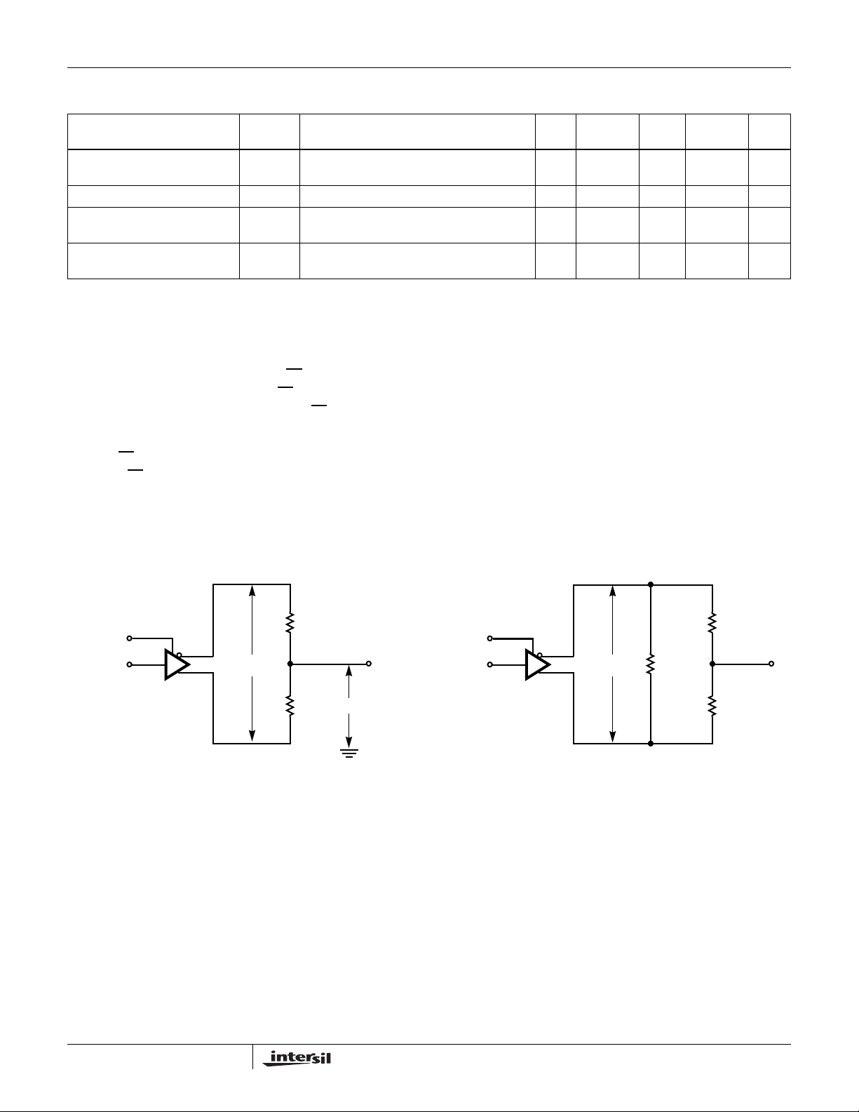
Test Circuits and Waveforms
DE
V
CC
DI
Z
D
Y
V
OD
FIGURE 1A. VOD AND V
RL/2
V
V
/2
R
OC
OC
L
FIGURE 1. DC DRIVER TEST CIRCUITS
DE
CC
DI
Z
D
Y
V
OD
RL = 60Ω
FIGURE 1B. VOD WITH COMMON MODE LOAD
375Ω
VCM
-7V TO +12V
375Ω
6
FN6587.1
February 18, 2008
Page 7
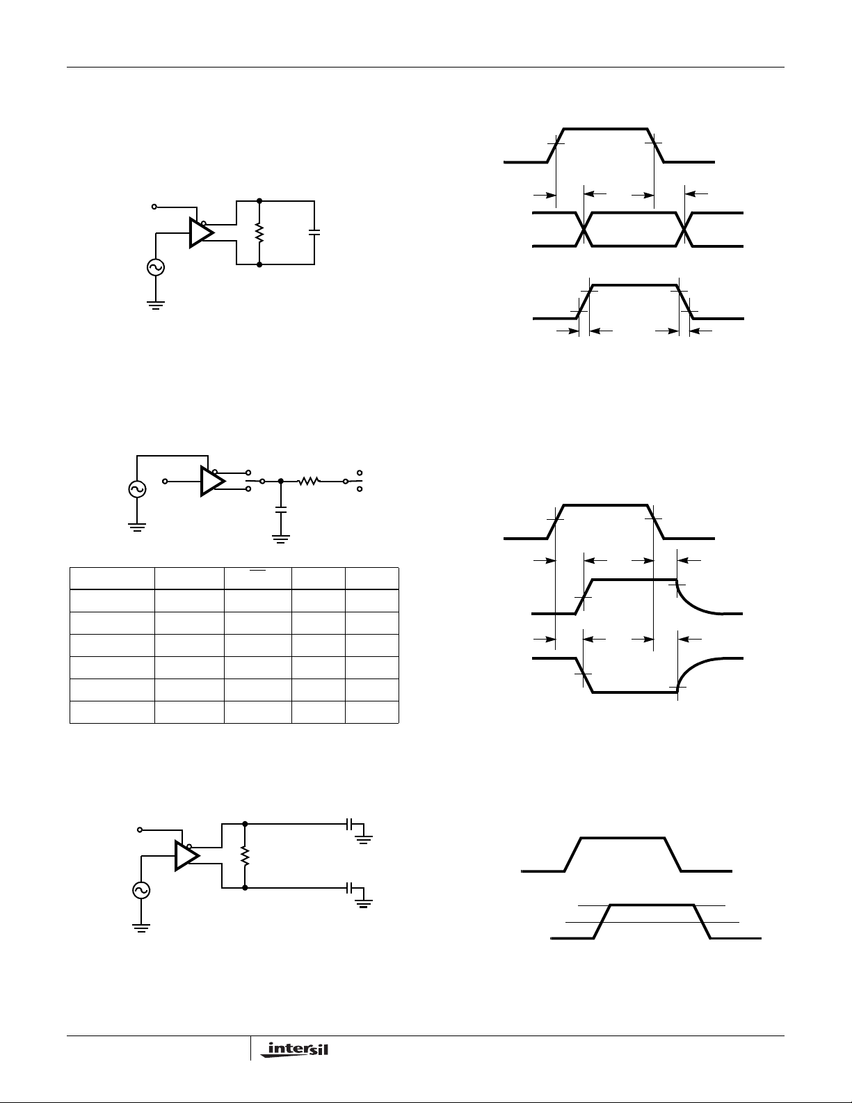
Test Circuits and Waveforms (Continued)
ISL3259E
3V
DI
1.5V1.5V
0V
DE
V
CC
SIGNAL
GENERATOR
DI
Z
D
Y
R
D
C
D
FIGURE 2A. TEST CIRCUIT
FIGURE 2. DRIVER PROPAGATION DELAY AND DIFFERENTIAL TRANSITION TIMES
DE
SIGNAL
GENERATOR
DI
Z
D
Y
110Ω
SW
50pF
PARAMETER OUTPUT RE DI SW
t
HZ
t
LZ
t
ZH
t
ZL
t
HZ(SHDN)
t
LZ(SHDN)
Y/Z X 1/0 GND
Y/Z X 0/1 V
Y/Z 0 (Note 8) 1/0 GND
Y/Z 0 (Note 8) 0/1 V
Y/Z 1 (Note 11) 1/0 GND
Y/Z 1 (Note 11) 0/1 V
V
CC
GND
CC
CC
CC
OUT (Z)
OUT (Y)
DIFF OUT (Y - Z)
FIGURE 2B. MEASUREMENT POINTS
DE
(NOTE 10)
tZH, t
ZH(SHDN)
(NOTE 10)
OUT (Y, Z)
, t
t
ZL
ZL(SHDN)
(NOTE 10)
OUT (Y, Z)
PLH
- t
t
PHL
t
t
PHL
|
1.5V1.5V
HZ
VOH - 0.5V
LZ
VOL + 0.5V
t
PLH
90% 90%
10% 10%
t
R
SKEW = |t
OUTPUT HIGH
50%
50%
OUTPUT LOW
V
OH
V
OL
+V
OD
-V
OD
t
F
3V
0V
V
OH
0V
V
CC
V
OL
V
CC
SIGNAL
GENERATOR
FIGURE 3A. TEST CIRCUIT
FIGURE 3B. MEASUREMENT POINTS
FIGURE 3. DRIVER ENABLE AND DISABLE TIMES
DE
DI
Z
D
Y
54Ω
+
C
L
V
OD
-
C
L
DI
DIFF OUT (Y - Z)
-V
OD
FIGURE 4A. TEST CIRCUIT FIGURE 4B. MEASUREMENT POINTS
FIGURE 4. DRIVER DATA RATE
7
3V
0V
+V
OD
0V
FN6587.1
February 18, 2008
Page 8
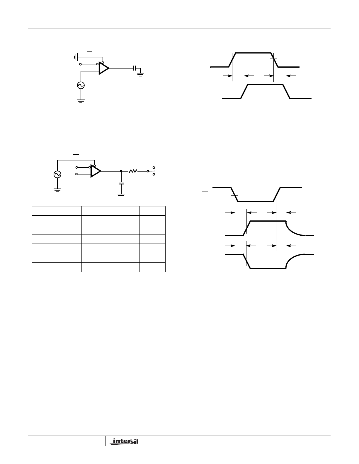
Test Circuits and Waveforms (Continued)
ISL3259E
RE
B
+1.5V
SIGNAL
GENERATOR
A
RO
R
FIGURE 5A. TEST CIRCUIT FIGURE 5B. MEASUREMENT POINTS
RE
B
A
RO
R
15pF
SIGNAL
GENERATOR
GND
PARAMETER DE A SW
t
HZ
t
LZ
t
(Note 9) 0 +1.5V GND
ZH
t
(Note 9) 0 -1.5V V
ZL
t
HZ(SHDN)
t
LZ(SHDN)
(Note 12) 0 +1.5V GND
(Note 12) 0 -1.5V V
0 +1.5V GND
0-1.5VV
15pF
A
RO
FIGURE 5. RECEIVER PROPAGATION DELAY
1kΩ
SW
CC
CC
CC
V
CC
GND
RE
tZH, t
ZH(SHDN)
(NOTE 10)
RO
t
, t
ZL
ZL(SHDN)
(NOTE 10)
RO
(NOTE 10)
t
PLH
1.7V 1.7V
OUTPUT HIGH
1.5V
1.5V
OUTPUT LOW
t
1.5V1.5V
PHL
t
t
1.5V1.5V
HZ
LZ
+3V
0V
3V
0V
VOH - 0.5V
VOL + 0.5V
V
CC
0V
V
OH
0V
V
CC
V
OL
FIGURE 6A. TEST CIRCUIT FIGURE 6B. MEASUREMENT POINTS
FIGURE 6. RECEIVER ENABLE AND DISABLE TIMES
8
FN6587.1
February 18, 2008
Page 9

ISL3259E
Application Information
RS-485 and RS-422 are differential (balanced) data
transmission standards for use in long haul or noisy
environments. RS-422 is a subset of RS-485, so RS-485
transceivers are also RS-422 compliant. RS-422 is a
point-to-multipoint (multidrop) standard, which allows only
one driver and up to 10 (assuming one unit load devices)
receivers on each bus. RS-485 is a true multipoint standard,
which allows up to 32 one unit load devices (any mix of
drivers and receivers) on each bus. To allow for multipoint
operation, the RS-485 spec requires that drivers must
handle bus contention without sustaining any damage.
Another important advantage of RS-485 is the extended
common mode range (CMR), which specifies that the driver
outputs and receiver inputs withstand signals that range from
+12V to -7V. RS-422 and RS-485 are intended for runs as
long as 4000’ (~1200m), so the wide CMR is necessary to
handle ground potential differences, as well as voltages
induced in the cable by external fields.
Receiver (Rx) Features
This transceiver utilizes a differential input receiver for
maximum noise immunity and common mode rejection. Input
sensitivity is ±200mV , as re quired by the RS-42 2 and RS-485
specifications. Receiver inputs function with common mode
voltages as great as 7V outside the power supplies (i.e.,
+12V and -7V), making them ideal for long networks, or
industrial environments, where induced voltages are a
realistic concern.
The receiver input resistance of 50kΩ surpasses the RS-422
spec of 4kΩ, and is 5x the RS-485 “Unit Load” (UL)
requirement of 12kΩ minimum. Thus, the ISL3259E is
known as a “one-fifth UL” transceiver, and there can be up to
160 devices on the RS-485 bus while still complying with the
RS-485 loading specification.
The receiver is a “full fail-safe” version that guarantees a
high level receiver output if the receiver inputs are
unconnected (floating), shorted together, or connected to a
terminated bus with all the transmitters disabled
(terminated/undriven).
Rx outputs deliver large low state currents (typically >30mA)
at V
= 1V, to ease the design of optically coupled isolated
OL
networks.
Receivers easily meet the 100Mbps data rate supported by
the driver, and the receiver output is tri-statable via the active
low RE
input.
Driver (Tx) Features
The RS-485/RS-422 driver is a differential output device that
delivers at least 2.1V across a 54Ω load (RS-485/
PROFIBUS), and at least 2.6V across a 100Ω load (RS-422)
even with V
delay skew to maximize bit width, and to minimize EMI.
= 4.75V. The drivers feature low propagation
CC
Outputs of the drivers are not slew rate limited, so faster
output transition times allow data rates up to100Mbps. Driver
outputs are tri-statable via the active high DE input.
For parallel applications, bit-to-bit skews between any two
ISL3259E transmitter and receiver pairs are guaranteed to
be no worse than 8ns (4ns max for any two Tx, 4ns max for
any two Rx).
High V
Improves Noise Immunity and Flexibilit y
OD
The ISL3259E driver design delivers larger differential output
voltages (VOD) than the RS-485 standard requires, or than
most RS-485 transmitters can deliver. The minimum ±2.1V
V
guarantees at least ±600mV more noise immunity than
OD
networks built using standard 1.5V V
transmitters.
OD
Another advantage of the large VOD is the ability to drive more
than two bus terminations, which allows for utilizing the
ISL3259E in “star” and other multi-terminated, “non-standard”
network topologies. Figure 8, details the transmitter’s V
I
characteristic, and includes load lines for four (30Ω) and
OUT
OD
vs
six (20Ω) 120Ω terminations. The figure shows that the driver
typically delivers 1.9/1.5V into 4/6 terminations, even at +85
The RS-485 standard requires a minimum 1.5V V
OD
°C.
into two
terminations, but the ISL3259E typically delivers RS-485
voltage levels with 2x to 3x the number of terminations.
ESD Protection
All pins on the ISL3259E include class 3 (>9kV) Human
Body Model (HBM) ESD protection structures, but the
RS-485 pins (driver outputs and receiver inputs)
incorporate advanced structures allowing them to survive
ESD events in excess of ±16.5kV HBM and ±15kV
IEC61000-4-2. The RS-485 pins are particularly vulnerable
to ESD strikes because they typically connect to an
exposed port on the exterior of the finished product. Simply
touching the port pins, or connecting a cable, can cause an
ESD event that might destroy unprotected ICs. These new
ESD structures protect the device whether or not it is
powered up, and without degrading the RS-485 common
mode range of -7V to +12V. This built-in ESD protection
eliminates the need for board level protection structures
(e.g., transient suppression diodes), and the associated,
undesirable capacitive load they present.
IEC61000-4-2 Testing
The IEC61000 test method applies to finished equipment,
rather than to an individual IC. Therefore, the pins most likely
to suffer an ESD event are those that are exposed to the
outside world (the RS-485 pins in this case), and the IC is
tested in its typical application configuration (power applied)
rather than testing each pin-to-pin combination. The
IEC61000 standard’s lower current limiting resistor coupled
with the larger charge storage capacitor yields a test that is
much more severe than the HBM test. The extra ESD
protection built into this device’s RS-485 pins allows the
design of equipment meeting level 4 criteria without the need
for additional board level protection on the RS-485 port.
9
FN6587.1
February 18, 2008
Page 10
ISL3259E
AIR-GAP DISCHARGE TEST METHOD
For this test method, a charged probe tip moves toward the
IC pin until the voltage arcs to it. The current waveform
delivered to the IC pin depends on approach speed,
humidity, temperature, etc., so it is more difficult to obtain
repeatable results. The ISL3259E RS-485 pins withstand
±15kV air-gap discharges.
CONTACT DISCHARGE TEST METHOD
During the contact discharge test, the probe contacts the
tested pin before the probe tip is energized, thereby
eliminating the variables associated with the air-gap
discharge. The result is a more repeatable and predictable
test, but equipment limits prevent testing devices at voltages
higher than ±9kV. The RS-485 pins of the ISL3259E survive
±8kV contact discharges.
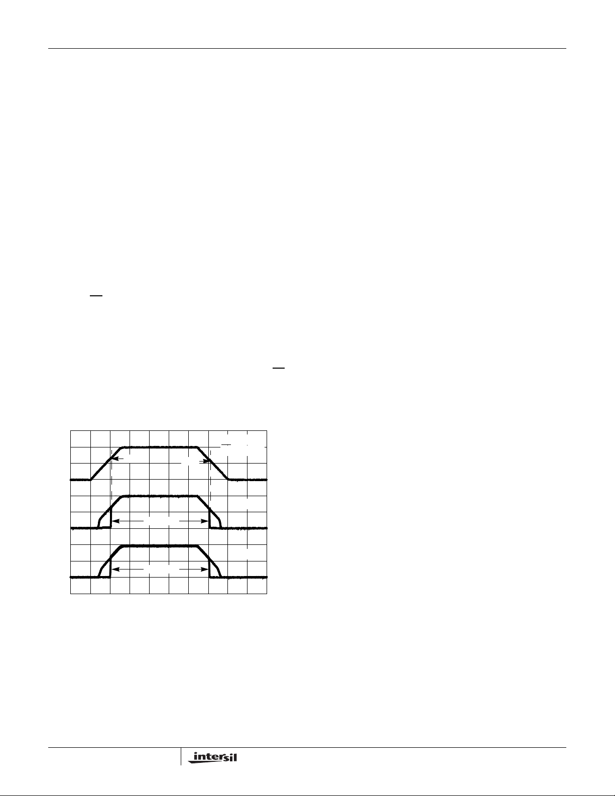
Hot Plug Function
When a piece of equipment powers up, there is a period of
time where the processor or ASIC driving the RS-485 control
lines (DE, RE
) is unable to ensure that the RS-485 Tx and
Rx outputs are kept disabled. If the equipment is connected
to the bus, a driver activating prematurely during power-up
may crash the bus. To avoid this scenario, the ISL3259E
incorporates a “Hot Plug” function. Circuitry monitoring V
CC
ensures that, during power-up and power-down, the Tx and Rx
outputs remain disabled, regardless of the state of DE and RE
if V
is less than ~3.2V . This gives the processor/ASIC a
CC
chance to stabilize and drive the RS-485 control lines to the
proper states.
DE, DI = V
3.3V
V
CC
5.0
2.5
A/Y
0
DRIVER Y OUTPUT (V)
RO
FIGURE 7. HOT PLUG PERFORMANCE (ISL3259E) vs
ISL83088E WITHOUT HOT PLUG CIRCUITRY
ISL3259E
ISL3259E
TIME (40μs/DIV)
3.1V
RE = GND
CC
RL = 1kΩ
RL = 1kΩ
5.0
2.5
0
5.0
2.5
0
Data Rate, Cables, and Terminations
Twisted pair is the cable of choice for RS-485, RS-422, and
PROFIBUS networks. Twisted pair cables tend to pick up
noise and other electromagnetically induced voltages as
common mode signals, which are effectively rejected by the
differential receivers in these ICs.
According to guidelines in the RS-422 and PROFIBUS
specifications, networks operating at data rates in excess of
3Mbps should be limited to cable lengths of 100m (328 ft) or
less, and the PROFIBUS specification recommends that the
more expensive “Type A” (22AWG) cable be used. The
ISL3259E’s large differential output swing, fast transition
times, and high drive-current output stages allow operation
even at 100Mbps over standard “CAT-5” cables up to 31m
(100 ft). Figures 16 and 17 detail the ISL3259E performance
at this condition, with a 120Ω termination resistor at both the
driver and the receiver ends. Note that the differential signal
delivered to the receiver at the end of the cable (A - B) still
exceeds 1V, so even longer cables could be driven if lower
noise margins are acceptable. Of course, jitter or some other
criteria may limit the network to shorter cable lengths than
those discussed here. If more noise margin is desired,
shorter cables may produce a larger receiver input signal.
Performance should be even better if the “Type A” cable is
utilized.
The ISL3259E may also be used at slower data rates over
longer cables, but there are some limitations. The Rx is
optimized for high speed operation, so its output may glitch if
the Rx input differential transition times are too slow.
Keeping the transition times below 500ns, (which equates to
the Tx driving a 1000’ (305m) CAT-5 cable) yields excellent
performance over the full operating temperature range.
,
T o minimize refle ctions, proper terminat ion is imperative when
using this high data rate transceiver. In point-to-point, or pointto-multipoint (single driver on bus) networks, the main cable
should be terminated in its characteristic impe dance (typically
120Ω for “CAT-5”, and 220Ω for “Type A”) at the end farthest
from the driver. In multi-receiver applications, stubs
(V)
CC
V
connecting receivers to the main cable should be kept as
short as possible. Multipoint (multi-driver) systems require that
the main cable be terminated in its characteristic impedance
at both ends. Stubs connecting a tra nsceiver to the main cable
should be kept as short as possible.
Built-In Driver Overload Protection
As stated previously, the RS-485 specification requires that
drivers survive worst case bus contentions undamaged.
These transmitters meet this requirement via driver output
short circuit current limits, and on-chip thermal shutdown
circuitry.
RECEIVER OUTPUT (V)
The driver output stages incorporate short circuit current limiting
circuitry, which ensures that the output current never exceeds
the RS-485 specification, even at the common mode voltage
range extremes. In the event of a major short circuit condition,
the device also includes a thermal shutdown feature that
disables the drivers whenever the die temperature becomes
excessive. This eliminates the power dissipation, allowing the
die to cool. The drivers automatically reenable after the die
temperature drops about +15°. If the contention persists, the
thermal shutdown/re-enable cycle repeats until the fault is
cleared. Receivers stay operational during thermal shutdown.
10
FN6587.1
February 18, 2008
Page 11
ISL3259E
Low Power Shutdown Mode
This BiCMOS transceiver uses a fraction of the power
required by their bipolar counterparts, but it also includes a
shutdown feature that reduces the already low quiescent I
to a 50nA trickle. It enters shutdown whenever the receiver
and driver are simultaneously disabled (RE
=VCC and
DE = GND) for a period of at least 600ns. Disabling both the
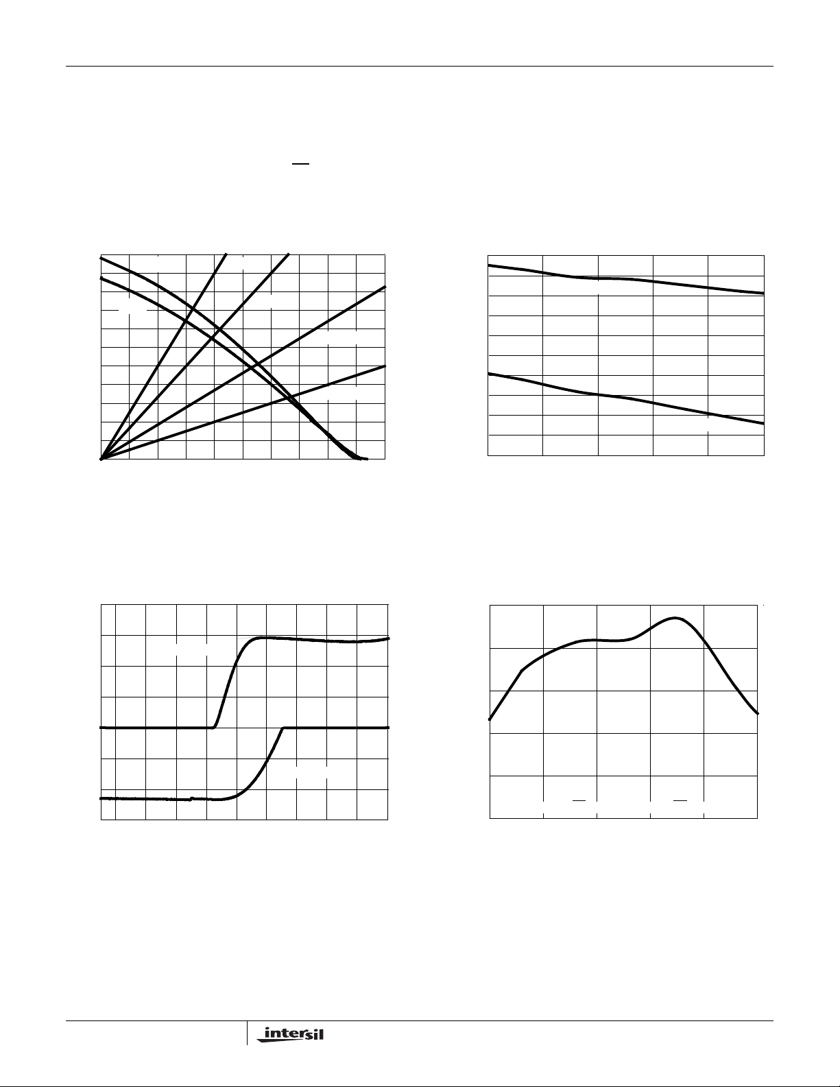
Typical Performance Curves V
DRIVER OUTPUT CURRENT (mA)
110
100
90
80
70
60
50
40
30
20
10
0
+25°C
+85°C
0 0.5 1.0 1.5 2.0 2.5 3.0 3.5 4.0 4.5 5.0
DIFFERENTIAL OUTPUT VOLTAGE (V)
FIGURE 8. DRIVER OUTPUT CURRENT vs DIFFERENTIAL
OUTPUT VOLTAGE
RD = 20Ω
RD = 30Ω
= 5V, TA = +25°C; Unless Otherwise Specified
CC
RD = 54Ω
RD = 100Ω
CC
driver and the receiver for less than 60ns guarantees that
the transceiver will not enter shutdown.
Note that receiver and driver enable times increase when
the transceiver enables from shutdown. Refer to Notes 8, 9,
10, 11 and 12, at the end of the “Electrical Specifications”
table on page 6, for more information.
3.5
3.4
3.3
3.2
3.1
3.0
2.9
2.8
2.7
2.6
DIFFERENTIAL OUTPUT VOLTAGE (V)
2.5
-40 -15 10 35 60 85
FIGURE 9. DRIVER DIFFERENTIAL OUTPUT VOLTAGE vs
TEMPERATURE
RD = 100Ω
RD = 54Ω
TEMPERATURE (°C)
200
150
Y OR Z = LOW
100
50
0
-50
OUTPUT CURRENT (mA)
-100
-150
-7 -6 -4 -2 0 2 4 6 8 10 12
OUTPUT VOLTAGE (V)
Y OR Z = HIGH
FIGURE 10. DRIVER OUTPUT CURRENT vs SHORT CIRCUIT
VOLTAGE
2.55
2.50
2.45
(mA)
CC
I
2.40
2.35
2.30
-40 -15 10 35 60 85
DE = VCC, RE = X OR DE = GND, RE = GND
TEMPERATURE (°C)
FIGURE 11. SUPPLY CURRENT vs TEMPERATURE
11
FN6587.1
February 18, 2008
Page 12
ISL3259E
Typical Performance Curves V
9.0
8.8
8.6
8.4
8.2
8.0
7.8
7.6
PROPAGATION DELAY (ns)
7.4
7.2
7.0
-40 -15 10 35 60 85
t
PHL
t
PLH
TEMPERATURE (°C)
= 5V, TA = +25°C; Unless Otherwise Specified (Continued)
CC
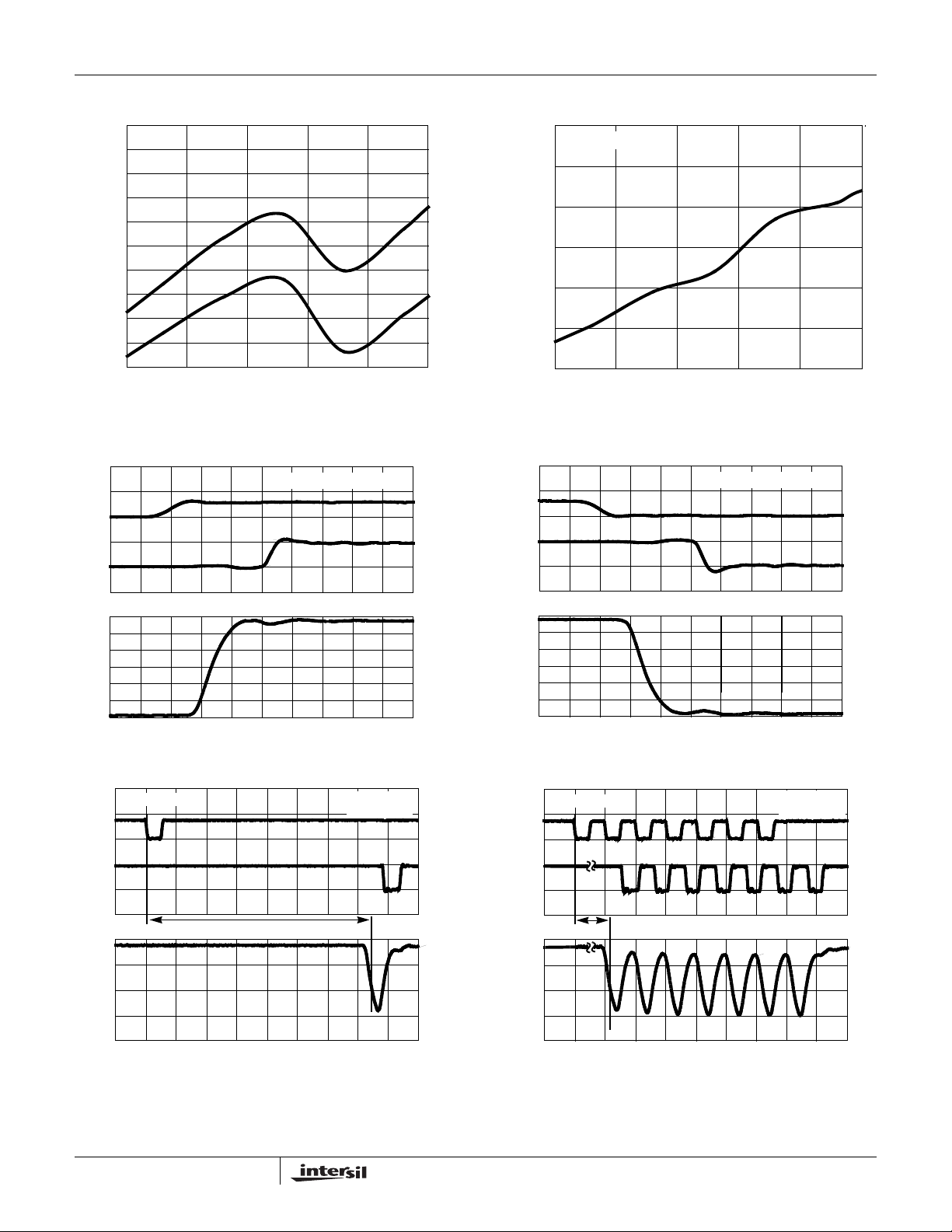
FIGURE 12. DRIVER DIFFERENTIAL PROPAGATION DELAY
vs TEMPERATURE
R
= 54Ω, CD = 50pF
DIFF
DI
5
0
RECEIVER OUTPUT (V)
RO
0.9
|t
- t
PHL
|
TEMPERATURE (°C)
PLH
0.8
0.7
0.6
SKEW (ns)
0.5
0.4
0.3
-40 -15 10 35 60 85
FIGURE 13. DRIVER DIFFERENTIAL SKEW vs
TEMPERATURE
R
= 54Ω, CD = 50pF
5
0
DRIVER INPUT (V)
5
0
RECEIVER OUTPUT (V)
DI
DIFF
RO
5
0
DRIVER INPUT (V)
3
2
1
0
Y-Z
-1
-2
DRIVER OUTPUT (V)
-3
TIME (5ns/DIV)
FIGURE 14. DRIVER AND RECEIVER WAVEFORMS
5.0
RECEIVER OUTPUT (V)
3.0
1.5
-1.5
-3.0
RECEIVER INPUT (V)
DI = 100Mbps
0
A - B
0
RO
DRIVER + CABLE DELAY (~150ns)
TIME (20ns/DIV)
= 4.75V
V
CC
T = +85°C
FIGURE 16. WORST CASE (NEGATIVE) SINGLE PULSE
DRIVER AND RECEIVER WAVEFORMS DRIVING
100 FEET (31 METERS) OF CAT5 CABLE
(DOUBLE TERMINATED WITH 120Ω)
3
2
1
0
Y-Z
-1
-2
-3
DRIVER OUTPUT (V)
TIME (5ns/DIV)
FIGURE 15. DRIVER AND RECEIVER WAVEFORMS
V
5
0
DRIVER INPUT (V)
DI = 100Mbps
5.0
RO
0
RECEIVER OUTPUT (V)
3.0
1.5
0
A - B
-1.5
-3.0
RECEIVER INPUT (V)
DRIVER + CABLE DELAY (~150ns)
TIME (20ns/DIV)
= 4.75V
CC
T = +85°C
5
0
DRIVER INPUT (V)
FIGURE 17. DRIVER AND RECEIVER SEVEN PULSE
WAVEFORMS DRIVING 100 FEET (31 METERS)
OF CAT5 CABLE (DOUBLE TERMINATED WITH
120Ω)
12
FN6587.1
February 18, 2008
Page 13
ISL3259E
Typical Performance Curves V
70
60
VOH, +25°C
50
40
30
20
10
RECEIVER OUTPUT CURRENT (mA)
0
012 3 45
RECEIVER OUTPUT VOLTAGE (V)
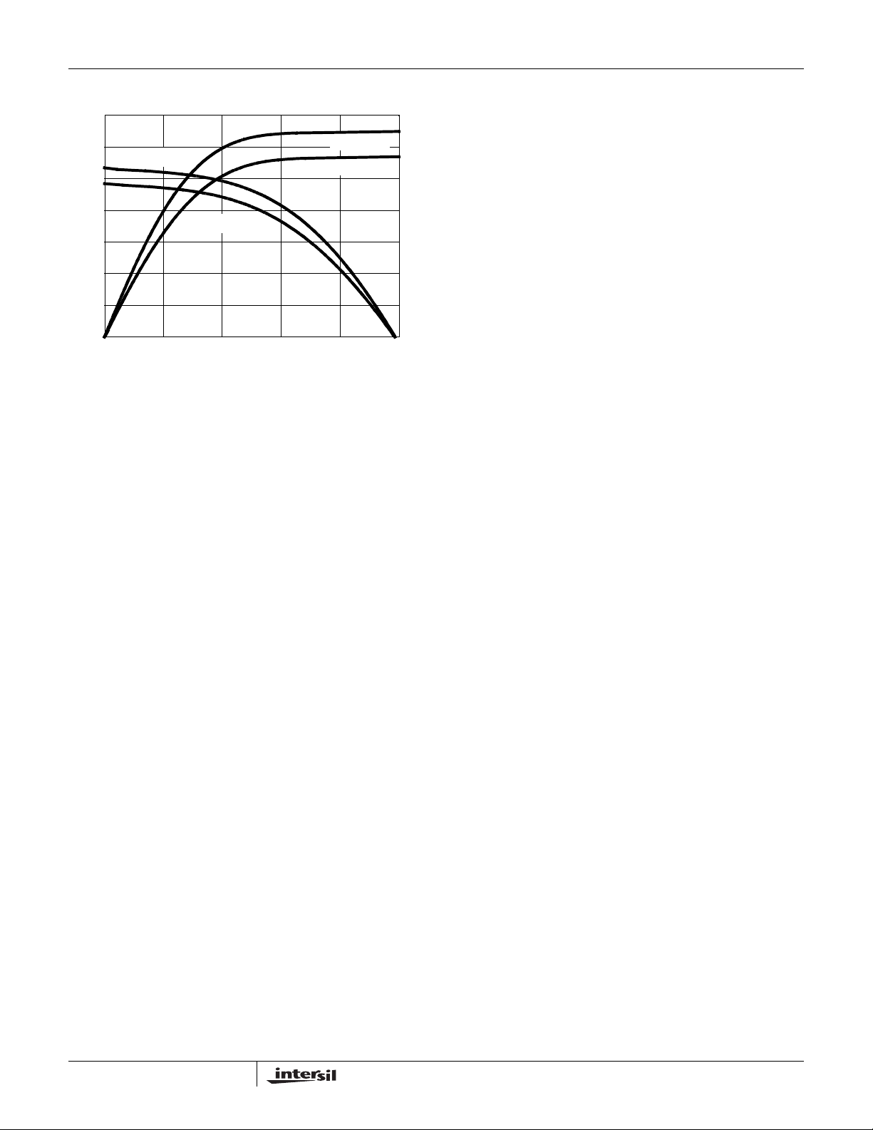
FIGURE 18. RECEIVER OUTPUT CURRENT vs RECEIVER
OUTPUT VOLTAGE
VOH, +85°C
= 5V, TA = +25°C; Unless Otherwise Specified (Continued)
CC
VOL, +25°C
VOL, +85°C
Die Characteristics
SUBSTRATE AND DFN THERMAL PAD POTENTIAL
(POWERED UP):
GND
TRANSISTOR COUNT:
768
PROCESS:
Si Gate BiCMOS
13
FN6587.1
February 18, 2008
Page 14
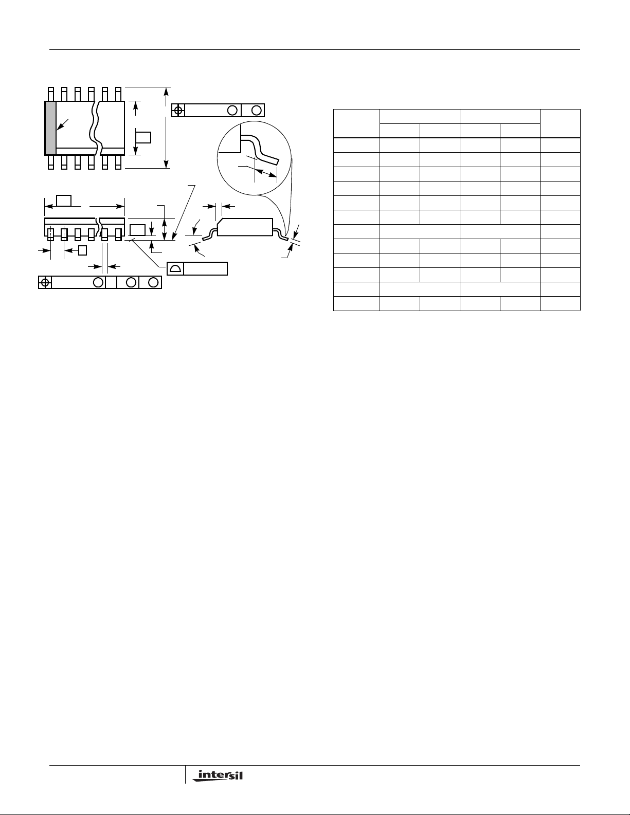
Small Outline Plastic Packages (SOIC)
ISL3259E
N
INDEX
AREA
123
-A-
E
-B-
SEATING PLANE
D
A
-C-
0.25(0.010) BM M
H
L
h x 45°
α
e
B
0.25(0.010) C AM BS
M
NOTES:
1. Symbols are defined in the “MO Series Symbol List” in Section 2.2 of
Publication Number 95.
2. Dimensioning and tolerancing per ANSI Y14.5M-1982.
3. Dimension “D” does not include mold flash, protrusions or gate burrs.
Mold flash, protrusion and gate burrs shall not exceed 0.15mm (0.006
inch) per side.
4. Dimension “E” does not include interlead flash or protrusions. Interlead flash and protrusions shall not exceed 0.25mm (0.010 inch) per
side.
5. The chamfer on the body is optional. If it is not present, a visual index
feature must be located within the crosshatched area.
6. “L” is the length of terminal for soldering to a substrate.
7. “N” is the number of terminal positions.
8. Terminal numbers are shown for reference only.
9. The lead width “B”, as measured 0.36mm (0.014 inch) or greater
above the seating plane, shall not exceed a maximum value of
0.61mm (0.024 inch).
10. Controlling dimension: MILLIMETER. Converted inch dimensions
are not necessarily exact.
A1
C
0.10(0.004)
M8.15 (JEDEC MS-012-AA ISSUE C)
8 LEAD NARROW BODY SMALL OUTLINE PLASTIC PACKAGE
INCHES MILLIMETERS
SYMBOL
A 0.0532 0.0688 1.35 1.75 -
A1 0.0040 0.0098 0.10 0.25 -
B 0.013 0.020 0.33 0.51 9
C 0.0075 0.0098 0.19 0.25 -
D 0.1890 0.1968 4.80 5.00 3
E 0.1497 0.1574 3.80 4.00 4
e 0.050 BSC 1.27 BSC -
H 0.2284 0.2440 5.80 6.20 -
h 0.0099 0.0196 0.25 0.50 5
L 0.016 0.050 0.40 1.27 6
N8 87
α
0° 8° 0° 8° -
NOTESMIN MAX MIN MAX
Rev. 1 6/05
14
FN6587.1
February 18, 2008
Page 15
ISL3259E
Mini Small Outline Plastic Packages (MSOP)
N
EE1
INDEX
AREA
AA1A2
TOP VIEW
-H-
SIDE VIEW
12
b
e
D
NOTES:
1. These package dimensions are within allowable dimensions of
JEDEC MO-187BA.
2. Dimensioning and tolerancing per ANSI Y14.5M-1994.
3. Dimension “D” does not include mold flash, protrusions or gate
burrs and are measured at Datum Plane. Mold flash, protrusion
and gate burrs shall not exceed 0.15mm (0.006 inch) per side.
4. Dimension “E1” does not include interlead flash or protrusions
and are measured at Datum Plane. Interlead flash and
protrusions shall not exceed 0.15mm (0.006 inch) per side.
5. Formed leads shall be planar with respect to one another within
0.10mm (0.004) at seating Plane.
6. “L” is the length of terminal for soldering to a substrate.
7. “N” is the number of terminal positions.
8. Terminal numbers are shown for reference only.
9. Dimension “b” does not include dambar protrusion. Allowable
dambar protrusion shall be 0.08mm (0.003 inch) total in excess
of “b” dimension at maximum material condition. Minimum space
between protrusion and adjacent lead is 0.07mm (0.0027 inch).
- H -
-A -
.
10. Datums and to be determined at Datum plane
11. Controlling dimension: MILLIMETER. Converted inch dimensions are for reference only.
-B-
0.20 (0.008) A
GAUGE
PLANE
SEATING
PLANE
0.10 (0.004) C
-A-
0.20 (0.008) C
- B -
0.25
(0.010)
-C-
SEATING
PLANE
a
0.20 (0.008) C
- H -
B
4X θ
C
D
4X θ
L1
C
L
E
1
END VIEW
R1
R
L
C
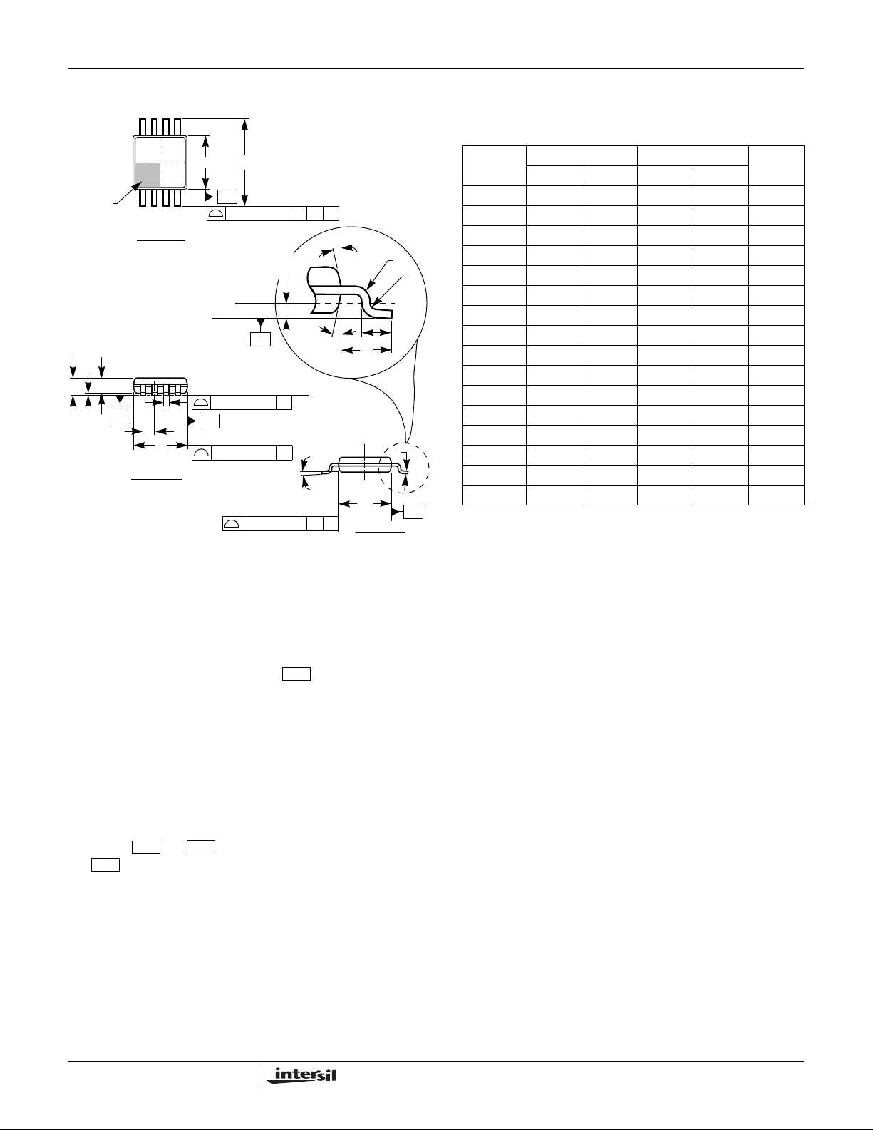
-B-
M8.118 (JEDEC MO-187AA)
8 LEAD MINI SMALL OUTLINE PLASTIC PACKAGE
INCHES MILLIMETERS
SYMBOL
A 0.037 0.043 0.94 1.10 A1 0.002 0.006 0.05 0.15 A2 0.030 0.037 0.75 0.95 -
b 0.010 0.014 0.25 0.36 9
c 0.004 0.008 0.09 0.20 -
D 0.116 0.120 2.95 3.05 3
E1 0.116 0.120 2.95 3.05 4
e 0.026 BSC 0.65 BSC -
E 0.187 0.199 4.75 5.05 -
L 0.016 0.028 0.40 0.70 6
L1 0.037 REF 0.95 REF -
N8 87
R 0.003 - 0.07 - R1 0.003 - 0.07 - -
0 5
α
o
o
0
15
o
o
6
o
5
o
0
15
o
o
6
Rev. 2 01/03
NOTESMIN MAX MIN MAX
-
-
15
FN6587.1
February 18, 2008
Page 16
Dual Flat No-Lead Plastic Package (DFN)
ISL3259E
(DAT UM B )
6
INDEX
AREA
(DATUM A)
NX (b)
5
SECTION "C-C"
6
INDEX
AREA
SEATING
PLANE
NX L
8
A
C
D
TOP
VIEW
SIDE VIEW
D2
D2/2
12
N
N-1
e
(Nd-1)Xe
REF .
BOTTOM VIEW
(A1)
2X
A3
E2/2
NX b
5
C
L
e
CC
FOR ODD TERMINAL/SIDE
87
0.10
ABC0.10
2X
0.10
E
//
A
NX k
E2
M
9
TERMINAL TIP
0.10
0.08
L
CB
BAC
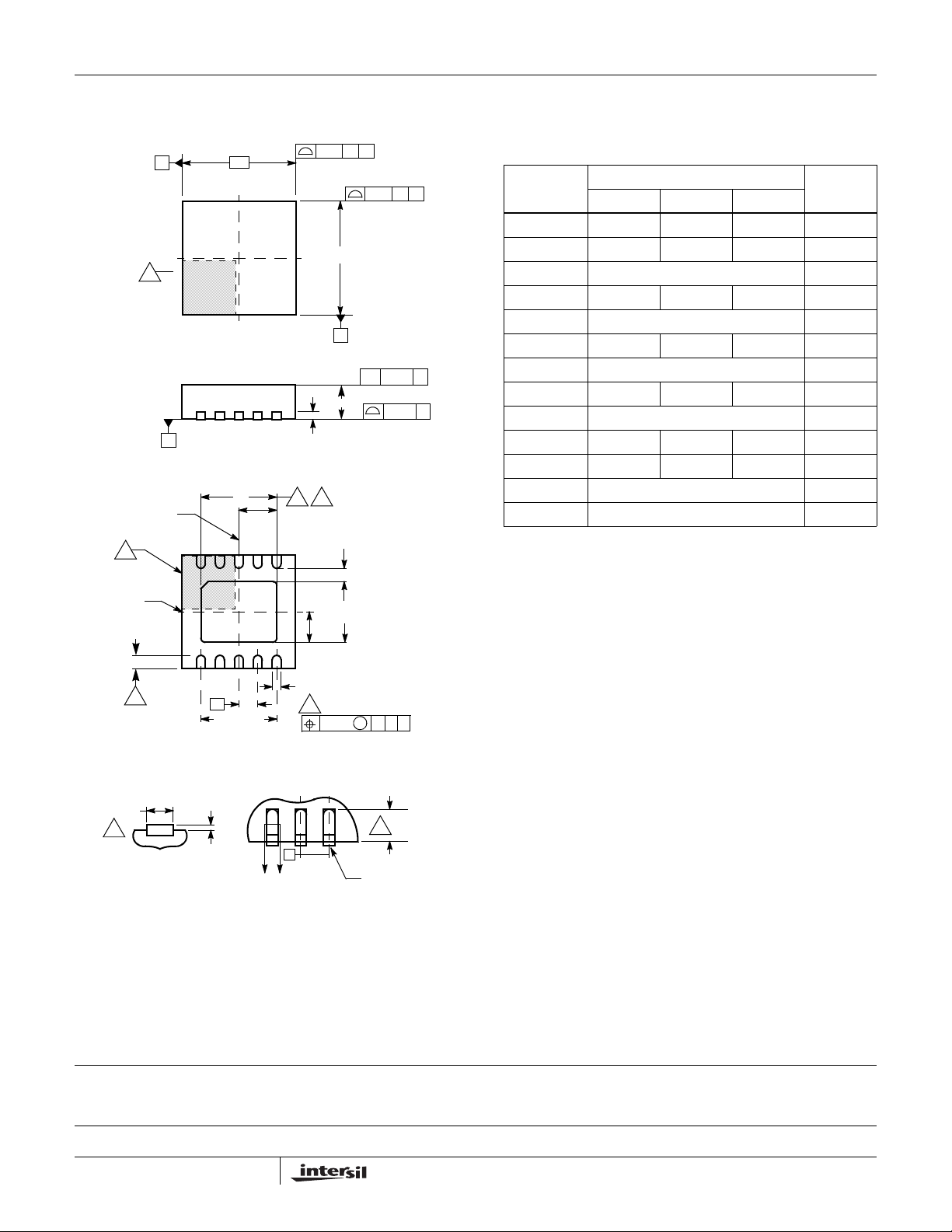
L10.3x3C
10 LEAD DUAL FLAT NO-LEAD PLASTIC PACKAGE
MILLIMETERS
SYMBOL
A 0.85 0.90 0.95 A1 - - 0.05 A3 0.20 REF -
b 0.20 0.25 0.30 5, 8
D 3.00 BSC D2 2.33 2.38 2.43 7, 8
C
E 3.00 BSC E2 1.59 1.64 1.69 7, 8
C
e 0.50 BSC k0.20- - L 0.35 0.40 0.45 8
N102
Nd 5 3
NOTES:
1. Dimensioning and tolerancing conform to ASME Y14.5-1994.
2. N is the number of terminals.
3. Nd refers to the number of terminals on D.
4. All dimensions are in millimeters. Angles are in degrees.
5. Dimension b applies to the metallized terminal and is measured
between 0.15mm and 0.30mm from the terminal tip.
6. The configuration of the pin #1 identifier is optional, but must be
located within the zone indicated. The pin #1 identi fier may be
either a mold or mark feature.
7. Dimensions D2 and E2 are for the exposed pads which provide
improved electrical and thermal performance.
8. Nominal dimensions are provided to assist with PCB Land
Pattern Design efforts, see Intersil Technical Brief TB389.
9. COMPLIANT TO JEDEC MO-229-WEED-3 except for
dimensions E2 & D2.
NOTESMIN NOMINAL MAX
Rev. 1 4/06
All Intersil U.S. products are manufactured, assembled and tested utilizing ISO9000 quality systems.
Intersil Corporation’s quality certifications can be viewed at www.intersil.com/design/quality
Intersil products are sold by description only. Intersil Corporation reserves the right to make changes in circuit design, software and/or specifications at any time without
notice. Accordingly, the reader is cautioned to verify that data sheets are current before placing orders. Information furnished by Intersil is believed to be accurate and
reliable. However, no responsibility is assumed by Intersil or its subsidiaries for its use; nor for any infringements of patents or other rights of third parties which may result
from its use. No license is granted by implicat ion or oth erwise u nde r any p a tent or p at ent r ights of Intersil or its subsidiaries.
For information regarding Intersil Corporation and its products, see www.intersil.com
16
FN6587.1
February 18, 2008
 Loading...