

Page 1

查询ISL28488FAZ供应商
®
ISL28288, ISL28488
Data Sheet June 28, 2007
Dual and Quad Micropower Single Supply
Rail-to-Rail Input and Output (RRIO)
Op-Amp
The ISL28288 and ISL28488 are dual and quad channel
micropower operational amplifiers optimized for single
supply operation over the 2.4V to 5V range. They can be
operated from one lithium cell or two Ni-Cd batteries. For
equivalent performance in a single channel op-amp
reference EL8188.
These devices feature an Input Range Enhancement Circuit
(IREC) which enables them to maintain CMRR performance
for input voltages 10% above the positive supply rail and to
100mV below the negative supply. The output operation is
rail to rail.
The ISL28288 and ISL28488 draw minimal supply current
while meeting excellent DC-accuracy, AC-performance,
noise and output drive specifications. The ISL28288
contains a power down enable pin that reduces the power
supply current to typically less than 4µA in the disabled
state.
Pinouts
ISL28288
(10 LD MSOP)
TOP VIEW
IN+_A
1
EN
_A
2
V-
3
EN
_B
4
IN+_B IN-_B
5 6
ISL28488
(16 LD QSOP)
TOP VIEW
1
OUT_A
IN-_A
2
-
IN+_A
3
V+
4
IN+_B IN+_C
5
IN-_B
6
+
+
-
10
IN-_A
-
9
+
+
-
OUT_A
8
V+
OUT_B
7
16
OUT_D
IN-_D
15
+
-
IN+_D
14
V-
13
12
-
+
IN-_C
11
FN6339.1
Features
• Low power 120µA typical supply current
• 1.5mV max offset voltage
• 30pA max input bias current
• 300kHz typical gain-bandwidth product
• 105dB typical PSRR
• 100dB typical CMRR
• Single supply operation down to 2.4V
• Input is capable of swinging above V+ and below V(ground sensing)
• Rail-to-rail input and output (RRIO)
• Enable Pin (ISL28288 only)
• Pb-free plus anneal available (RoHS compliant)
Applications
• Battery- or solar-powered systems
• 4mA to 25mA current loops
• Handheld consumer products
• Medical devices
• Thermocouple amplifiers
• Photodiode pre-amps
• pH probe amplifiers
Ordering Information
PART NUMBER
(Note)
ISL28288FUZ 8288Z 10 Ld MSOP MDP0043
ISL28288FUZ-T7 8288Z 10 Ld MSOP MDP0043
ISL28488FAZ 28488 FAZ 16 Ld QSOP MDP0040
ISL28488FAZ-T7 28488 FAZ 16 Ld QSOP MDP0040
*“-T7” suffix is for tape and reel. Please refer to TB347 for details on
reel specifications.
NOTE: Intersil Pb-free plus anneal products employ special Pb-free
material sets; molding compounds/die attach materials and 100%
matte tin plate termination finish, which are RoHS compliant and
compatible with both SnPb and Pb-free soldering operations.
Intersil Pb-free products are MSL classified at Pb-free peak reflow
temperatures that meet or exceed the Pb-free requirements of
IPC/JEDEC J STD-020.
PART
MARKING
PACKAGE
(Pb-Free)
PKG. DWG.
#
OUT_B
7
NC NC
8 9
1
10
OUT_C
CAUTION: These devices are sensitive to electrostatic discharge; follow proper IC Handling Procedures.
1-888-INTERSIL or 1-888-468-3774
| Intersil (and design) is a registered trademark of Intersil Americas Inc.
Copyright Intersil Americas Inc. 2006, 2007. All Rights Reserved
All other trademarks mentioned are the property of their respective owners.
Page 2

ISL28288, ISL28488
Absolute Maximum Ratings (T
Supply Voltage. . . . . . . . . . . . . . . . . . . . . . . . . . . . . . . . . . . . . . 5.5V
Supply Turn On Voltage Slew Rate . . . . . . . . . . . . . . . . . . . . . 1V/μs
Differential Input Current . . . . . . . . . . . . . . . . . . . . . . . . . . . . . . 5mA
Differential Input Voltage . . . . . . . . . . . . . . . . . . . . . . . . . . . . . . 0.5V
Input Voltage . . . . . . . . . . . . . . . . . . . . . . . . . V-
ESD Tolerance
Human Body Model . . . . . . . . . . . . . . . . . . . . . . . . . . . . . . . . .3kV
Machine Model. . . . . . . . . . . . . . . . . . . . . . . . . . . . . . . . . . . .300V
= +25°C) Thermal Information
A
Thermal Resistance θ
10 Ld MSOP Package . . . . . . . . . . . . . . . . . . . . . . . 115
16 Ld QSOP Package . . . . . . . . . . . . . . . . . . . . . . . 112
- 0.5V to V+ + 0.5V
Output Short-Circuit Duration . . . . . . . . . . . . . . . . . . . . . . .Indefinite
Ambient Operating Temperature Range . . . . . . . . .-40°C to +125°C
Storage Temperature Range . . . . . . . . . . . . . . . . . .-65°C to +150°C
Operating Junction Temperature . . . . . . . . . . . . . . . . . . . . . +125°C
Pb-free reflow profile . . . . . . . . . . . . . . . . . . . . . . . . . .see link below
(°C/W)
JA
http://www.intersil.com/pbfree/Pb-FreeReflow.asp
CAUTION: Do not operate at or near the maximum ratings listed for extended periods of time. Exposure to such conditions may adversely impact product reliability and
result in failures not covered by warranty.
IMPORTANT NOTE: All parameters having Min/Max specifications are guaranteed. Typical values are for information purposes only. Unless otherwise noted, all tests
are at the specified temperature and are pulsed tests, therefore: T
Operating Junction
Electrical Specifications V
= 5V, V- = 0V, VCM = 2.5V, RL = Open, TA = +25°C unless otherwise specified.
+
= TC = T
J
A
Boldface limits apply over the operating temperature range, -40°C to +125°C. Temperature data
established by characterization
PARAMETER DESCRIPTION CONDITIONS
MIN
(Note 1) TYP
MAX
(Note 1) UNIT
DC SPECIFICATIONS
V
OS
ΔV
OS
------------------
ΔTi me
ΔV
OS
--------------- -
ΔT
I
OS
I
B
Input Offset Voltage -1.5
-2
±0.05 1.5
mV
2
Long Term Input Offset Voltage Stability ISL28288 1.2 µV/Mo
Input Offset Voltage vs Temperature 0.9 µV/°C
Input Offset Current
-40°C to +85°C
Input Bias Current
-40°C to +85°C
-30
-80
-30
-80
±530
80
±10 30
80
pA
pA
CMIR Common-Mode Voltage Range Guaranteed by CMRR 05V
CMRR Common-Mode Rejection Ratio V
PSRR Power Supply Rejection Ratio V
= 0V to 5V 80
CM
= 2.4V to 5V 85
+
75
100 dB
105 dB
80
A
V
VOL
OUT
Large Signal Voltage Gain VO = 0.5V to 4.5V, RL = 100kΩ 200
190
V
= 0.5V to 4.5V, RL = 1kΩ 60 V/mV
O
Maximum Output Voltage Swing Output low, RL = 100kΩ 3630mV
300 V/mV
I
S,ON
Output low, R
Output high, R
= 1kΩ 130 175
L
= 100kΩ 4.990
L
4.996 V
225
4.97
Output high, R
= 1kΩ 4.800
L
4.750
4.880 V
Quiescent Supply Current, Enabled ISL28288, All channels enabled. 120 156
175
ISL28488, All channels enabled. 240 315
350
2
mV
µA
µA
FN6339.1
June 28, 2007
Page 3

ISL28288, ISL28488
Electrical Specifications V
= 5V, V- = 0V, VCM = 2.5V, RL = Open, TA = +25°C unless otherwise specified.
+
Boldface limits apply over the operating temperature range, -40°C to +125°C. Temperature data
established by characterization (Continued)
MIN
PARAMETER DESCRIPTION CONDITIONS
I
S,OFF
+ Short Circuit Sourcing Capability RL = 10Ω 29
I
O
I
- Short Circuit Sinking Capability RL = 10Ω 24
O
Quiescent Supply Current, Disabled
(ISL28288)
All channels disabled. 4 7
(Note 1) TYP
24
20
V
SUPPLY
V
ENH
V
ENL
I
ENH
I
ENL
Supply Operating Range V+ to V- 2.4 5.0 V
EN Pin High Level (ISL28288) 2 V
EN Pin Low Level (ISL28288) 0.8 V
EN Pin Input High Current (ISL28288) VEN = V
EN Pin Input Low Current (ISL28288) VEN = V
+
-
AC SPECIFICATIONS
GBW Gain Bandwidth Product A
e
n
Input Noise Voltage Peak-to-Peak f = 0.1Hz to 10Hz 5.4 µV
= 100, RF = 100kΩ, RG = 1kΩ,
V
R
= 10kΩ to V
L
CM
Input Noise Voltage Density fO = 1kHz 48 nV/√Hz
i
n
CMRR @ 60Hz Input Common Mode Rejection Ratio V
PSRR+ @
120Hz
PSRR- @
120Hz
Input Noise Current Density fO = 1kHz 0.1 pA/√Hz
= 1V
, RL = 10kΩ to V
P-P
= 1V
, RL = 10kΩ to V
P-P
= 1V
, RL = 10kΩ to V
P-P
CM
CM
CM
Power Supply Rejection Ratio (V
Power Supply Rejection Ratio (V
CM
)V
+
)V
-
, V- = ±1.2V and ±2.5V,
+
V
SOURCE
, V- = ±1.2V and ±2.5V
+
V
SOURCE
TRANSIENT RESPONSE
SR Slew Rate
t
EN
Enable to Output Turn-on Delay Time,
10% EN
Enable to Output Turn-off Delay Time,
10% EN
to 10% Vout, (ISL28288)
to 10% Vout, (ISL28288)
VEN
= 5V to 0V, AV = -1,
RG = RF = RL = 1k
= 0V to 5V, AV = -1,
VEN
RG = RF = RL = 1k
to V
to V
±0.12
±0.09
CM
CM
±0.14 ±0.16
NOTE:
1. Parts are 100% tested at +25°C. Over temperature limits established by characterization and are not production tested.
MAX
(Note 1) UNIT
µA
9
31 mA
26 mA
0.8 1
µA
1.5
0 +0.1 µA
300 kHz
P-P
-70 dB
-80 dB
-60 dB
V/µs
±0.21
2µs
0.1 µs
3
FN6339.1
June 28, 2007
Page 4

ISL28288, ISL28488
Typical Performance Curves V
+1
0
-1
-2
-3
-4
GAIN (dB)
-5
V
AV = 1
-6
C
R
-7
8
1k
V+, V-= ±2.5V
RL = 1k
V+, V- = ±2.5V
RL = 10k
= 50mV
OUT
= 3pF
L
= 0, RG = INF
F
P-P
10k 100k 1M
FREQUENCY (Hz)
= 5V, V- = 0V, VCM = 2.5V, RL = Open
+
V+, V- = ±1.2V
RL = 1k
V+, V- = ±1.2V
RL = 10k
5M
FIGURE 1. FREQUENCY RESPONSE vs SUPPLY VOLTAGE
120
80
40
GAIN (dB)
0
-40
-80
11k100k10M
10
FREQUENCY (Hz)
FIGURE 3. A
vs FREQUENCY @ 100kΩ LOAD
VOL
10k 1M100
80
40
0
-40
-80
-120
45
40
35
30
25
20
AV = 100
GAIN (dB)
15
= 10kΩ
R
L
C
= 3pF
L
10
= 100kΩ
R
F
= 1kΩ
R
G
5
0
100 10k 100k 1M
V+, V- = ±1.0V
1k
FREQUENCY (Hz)
V+, V- = ±2.5V
V+, V- = ±1.2V
FIGURE 2. FREQUENCY RESPONSE vs SUPPLY VOLTAGE
100
80
60
PHASE (°)
40
GAIN (dB)
20
0
-20
10 10k 1M
FIGURE 4. A
100
FREQUENCY (Hz)
VOL
PHASE
GAIN
100k1k
vs FREQUENCY @ 1kΩ LOAD
200
150
100
50
0
-50
-100
-150
PHASE (°)
10
= 5VDC
V
+
0
V
-10
RL = 10kΩ
-20
A
-30
-40
-50
PSRR (dB)
-60
-70
-80
-90
-100
10 100 1k 10k 100k
SOURCE
= +1
V
= 1V
P-P
PSRR -
FREQUENCY (Hz)
PSRR +
1M
10
0
, V- = ±2.5VDC
V
+
V
-10
RL = 10kΩ
-20
-30
-40
-50
-60
CMRR (dB)
-70
-80
-90
-100
10 100 1k 10k 100k
SOURCE
= 1V
P-P
FREQUENCY (Hz)
FIGURE 5. PSRR vs FREQUENCY FIGURE 6. CMRR vs FREQUENCY
4
1M
FN6339.1
June 28, 2007
Page 5
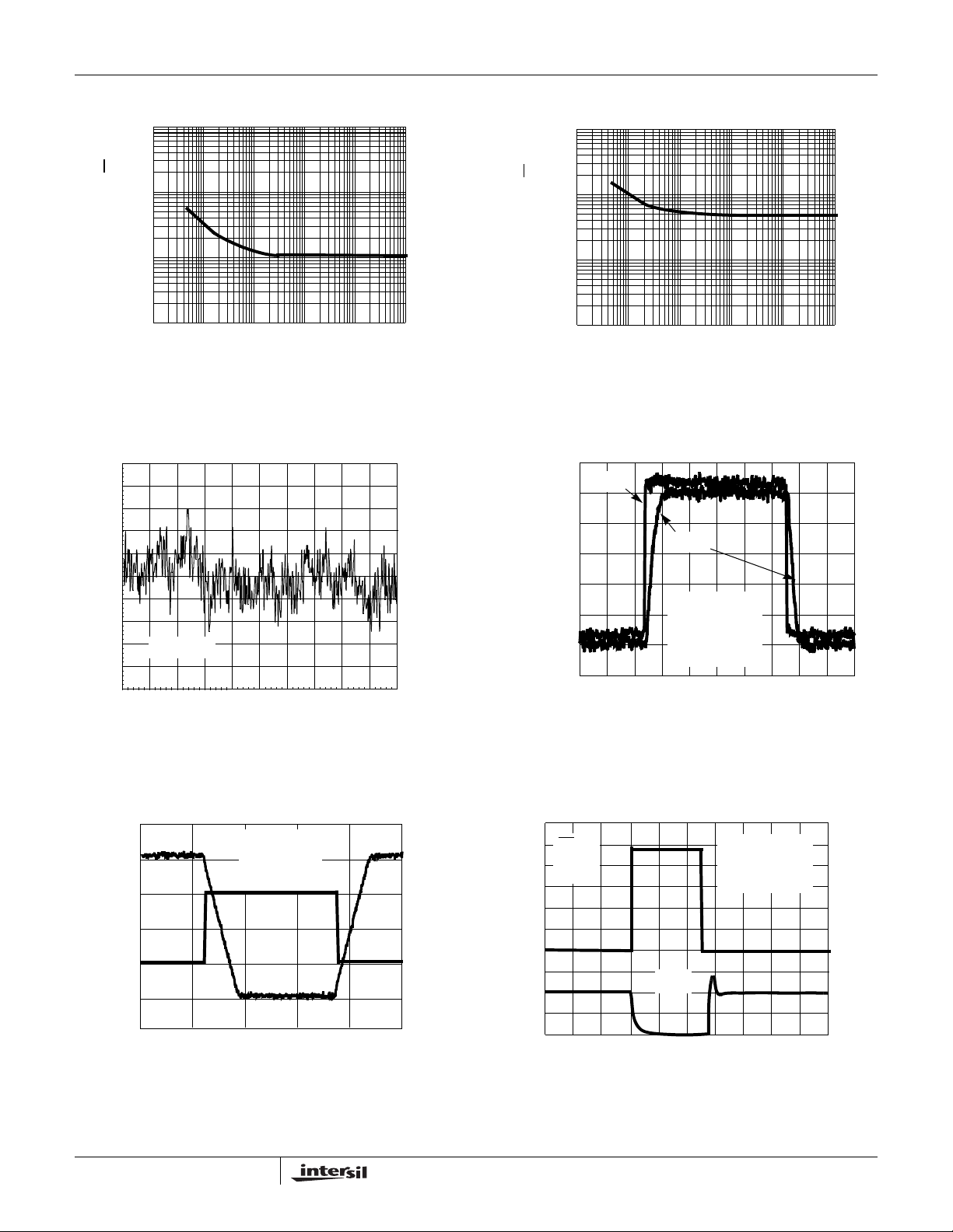
ISL28288, ISL28488
Typical Performance Curves V
10.00
1.00
0.10
CURRENT NOISE (pA/√Hz)
0.01
1 10 100 1k 10k
FREQUENCY (Hz)
FIGURE 7. CURRENT NOISE vs FREQUENCY FIGURE 8. VOLTAGE NOISE vs FREQUENCY
= 5V, V- = 0V, VCM = 2.5V, RL = Open (Continued)
+
1k
100
10
VOLTAGE NOISE (nV/√Hz)
100k
1
1 10 100 10k 100k
2.56
V
2.54
2.52
2.50
IN
1k
FREQUENCY (Hz)
V
OUT
2.48
= 5VDC
V
+
V
= 0.1V
OUT
RL = 1kΩ
A
= +1
V
TIME (µs)
P-P
VOLTAGE NOISE (1µV/DIV)
5.4µV
P-P
TIME (1s/DIV)
VOLTS (V)
2.46
2.44
2.42
0 2 4 6 8 101214161820
FIGURE 9. 0.1Hz TO 10Hz INPUT VOLTAGE NOISE FIGURE 10. SMALL SIGNAL TRANSIENT RESPONSE
VOLTS (V)
5.0
4.0
3.0
2.0
1.0
0
V
= 5VDC
+
V
= 2V
OUT
RL = 1kΩ
A
= -2
V
P-P
V
V
OUT
IN
EN
INPUT
1V/DIV0.1V/DIV
0
V
OUT
AV = -1
= 200mV
V
IN
V+ = 5V
= 0V
V
-
P-P
0 50 100 150 200 250
TIME (µs)
FIGURE 11. LARGE SIGNAL TRANSIENT RESPONSE
5
0
10µs/DIV
FIGURE 12. ENABLE TO OUTPUT DELAY TIME
FN6339.1
June 28, 2007
Page 6
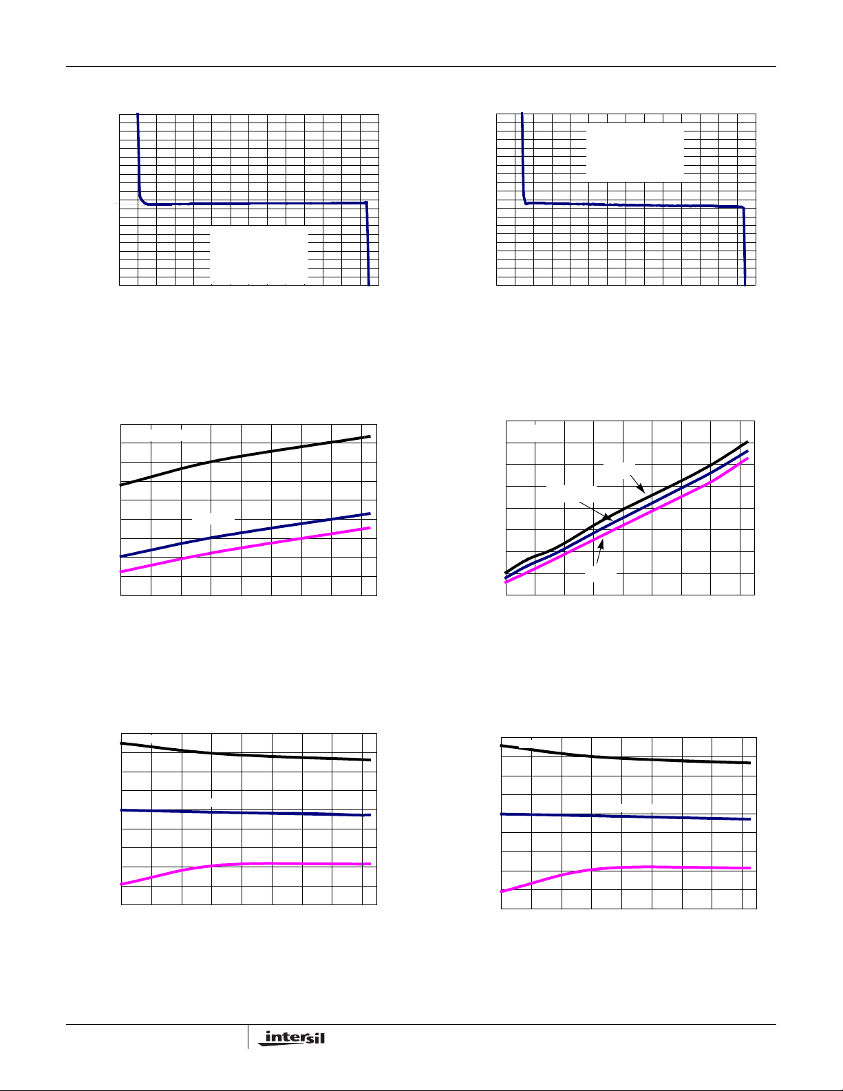
ISL28288, ISL28488
Typical Performance Curves V
1000
800
600
400
200
(µV)
0
OS
V
-200
-400
-600
-800
-1000
-10123456
V+ = 5V
= OPEN
R
L
= 100k, RG = 100
R
F
= +1000
A
V
(V)
V
CM
= 5V, V- = 0V, VCM = 2.5V, RL = Open (Continued)
+
FIGURE 13. INPUT OFFSET VOLTAGE vs COMMON MODE
INPUT VOLTAGE
350
N = 1000
330
310
290
270
250
CURRENT (µA)
230
210
190
170
-40 -20 0 20 40 60 80 100 120
MAX
MEDIAN
MIN
TEMPERATURE (°C)
FIGURE 15. ISL28488 SUPPL Y CURRENT vs TEMPERA TURE
V
, V- = ±2.5V ENABLED, RL = INF
+
100
80
60
40
20
(pA)
0
-20
-BIAS
I
-40
-60
-80
-100
-10123456
V+ = 5V
= OPEN
R
L
= 100k, RG = 100
R
F
A
= +1000
V
V
(V)
CM
FIGURE 14. INPUT BIAS CURRENT vs COMMON-MODE
INPUT VOLTAGE
4.8
n = 12
4.6
4.4
4.2
4
3.8
CURRENT (µA)
3.6
3.4
3.2
-40-200 20406080100120
MEDIAN
MAX
MIN
TEMPERATURE (°C)
FIGURE 16. ISL28288 SUPPL Y CURRENT vs TEMPERA TURE
V
, V- = ±2.5V DISABLED, RL = INF
+
2
N = 1000
1.5
1
0.5
(mV)
0
OS
V
-0.5
-1
-1.5
-2
-2.5
-40-200 20406080100120
FIGURE 17. V
vs TEMPERATURE, V
OS
MAX
MEDIAN
MIN
TEMPERATURE (°C)
= 0V, V+, V- = ±2.5V
IN
6
2
N = 1000
1.5
1
0.5
(mV)
0
OS
V
-0.5
-1
-1.5
-2
-2.5
-40 -20 0 20 40 60 80 100 120
TEMPERATURE (°C)
FIGURE 18. V
vs TEMPERATURE V
OS
MAX
MEDIAN
MIN
IN
= 0V, V+, V- = ±1.2V
FN6339.1
June 28, 2007
Page 7
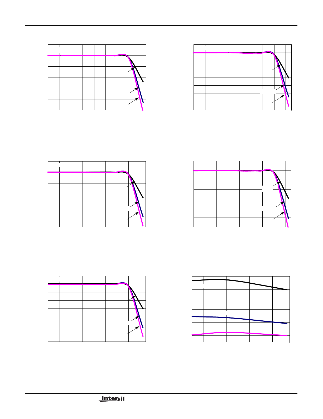
ISL28288, ISL28488
Typical Performance Curves V
500
n = 1000
0
-500
(pA)
-1000
BIAS+
I
-1500
-2000
-2500
-40 -20 0 20 40 60 80 100 120
TEMPERATURE (°C)
FIGURE 19. I
500
n = 1000
0
-500
(pA)
-1000
BIAS+
I
-1500
-2000
-2500
-40 -20 0 20 40 60 80 100 120
FIGURE 21. I
vs TEMPERATURE V+, V- = ±2.5V FIGURE 20. I
BIAS+
TEMPERATURE (°C)
+ vs TEMPERATURE V+, V- = ±1.2V
BIAS
= 5V, V- = 0V, VCM = 2.5V, RL = Open (Continued)
+
200
n = 1000
0
-200
MAX
MEDIAN
MIN
MAX
MEDIAN
MIN
-400
(pA)
-600
BIAS-
-800
I
-1000
-1200
-1400
-40 -20 0 20 40 60 80 100 120
200
n = 1000
0
-200
-400
(pA)
-600
BIAS-
I
-800
-1000
-1200
-40 -20 0 20 40 60 80 100 120
FIGURE 22. I
MEDIAN
TEMPERATURE (°C)
- vs TEMPERATURE V+, V- = ±2.5V
BIAS
MAX
MEDIAN
TEMPERATURE (°C)
- vs TEMPERATURE V+, V- = ±-1.2V
BIAS
MAX
MIN
MIN
200
n = 1000
0
-200
-400
(pA)
-600
OS
I
-800
-1000
-1200
-1400
-40 -20 0 20 40 60 80 100 120
TEMPERATURE (°C)
FIGURE 23. I
vs TEMPERATURE V+, V- = ±2.5V
OS
MEDIAN
7
MAX
MIN
650
600
n = 1000
550
500
450
(V/mV)
400
VOL
350
A
300
250
200
150
-40 -20 0 20 40 60 80 100 120
FIGURE 24. A
vs TEMPERATURE V+, V- = ±2.5V , RL=100k
VOL
MAX
MEDIAN
MIN
TEMPERATURE (°C)
FN6339.1
June 28, 2007
Page 8
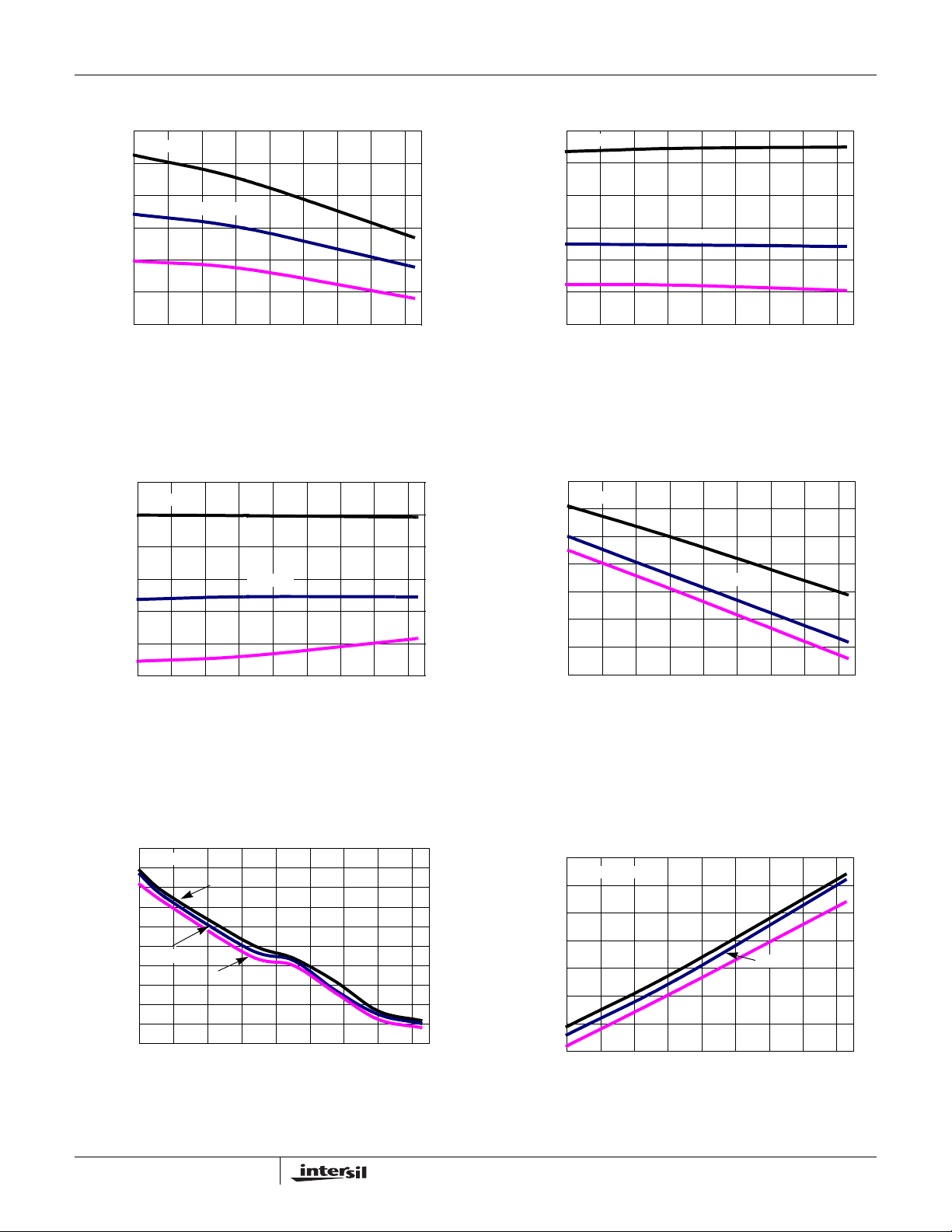
ISL28288, ISL28488
Typical Performance Curves V
90
n = 1000
80
70
60
(V/mV)
VOL
A
50
40
30
-40 -20 0 20 40 60 80 100 120
FIGURE 25. A
140
130
120
110
PSRR (dB)
100
90
MEDIAN
vs TEMPERATURE, V+, V- = ±2.5V, RL=1k
VOL
n = 1000
MAX
MIN
TEMPERATURE (°C)
MAX
MEDIAN
MIN
= 5V, V- = 0V, VCM = 2.5V, RL = Open (Continued)
+
135
n = 1000
125
115
105
CMRR (dB)
95
85
75
-40 -20 0 20 40 60 80 100 120
FIGURE 26. CMRR vs TEMPERATURE V
V
, V- = ±2.5V
+
4.91
n = 1000
VOUT (V)
4.90
4.89
4.88
4.87
4.86
4.85
MAX
MEDIAN
MIN
TEMPERATURE (°C)
CM
MAX
MEDIAN
MIN
= +2.5V TO -2.5V ,
80
-40 -20 0 20 40 60 80 100 120
TEMPERATURE (°C)
FIGURE 27. PSRR vs TEMPERATURE, V
4.9984
4.9982
4.9980
4.9978
4.9976
4.9974
4.9972
VOUT (V)
4.9970
4.9968
4.9966
4.9964
FIGURE 29. V
n = 12
MAX
MEDIAN
MIN
-40 -20 0 20 40 60 80 100 120
TEMPERATURE (°C)
HIGH vs TEMPERATURE,
OUT
V
= ±2.5V, RL= 100k
+, V-
= ±1.2V TO ±2.75V
+, V-
4.84
-40 -20 0 20 40 60 80 100 120
TEMPERATURE (°C)
FIGURE 28. V
170
160
150
140
130
VOUT (mV)
120
110
100
-40 -20 0 20 40 60 80 100 120
FIGURE 30. V
HIGH vs TEMPERATURE,
OUT
V
= ±2.5V, RL= 1k
+, V-
n = 1000
MIN
TEMPERATURE (°C)
LOW vs TEMPERATURE,
OUT
V
= ±2.5V, RL= 1k
+, V-
MAX
MEDIAN
8
FN6339.1
June 28, 2007
Page 9
ISL28288, ISL28488
Typical Performance Curves V
4.3
n = 12
4.2
4.1
4.0
3.9
(mV)
3.8
OUT
V
3.7
3.6
3.5
3.4
-40 -20 0 20 40 60 80 100 120
FIGURE 31. V
MEDIAN
LOW vs TEMPERATURE,
OUT
V
= ±2.5V, RL= 100k
+, V-
MAX
MIN
TEMPERATURE (°C)
= 5V, V- = 0V, VCM = 2.5V, RL = Open (Continued)
+
39
n = 1000
37
35
33
(mA)
31
29
27
+OUTPUT SHORT CIRCUIT CURRENT
25
-40 -20 0 20 40 60 80 100 120
FIGURE 32. +OUTPUT SHORT CIRCUIT CURRENT vs
TEMPERATURE V
V
+, V-
-21
n = 1000
-23
-25
MAX
TEMPERATURE (°C)
= ±2.5V
MAX
MEDIAN
MIN
= +2.5V, RL = 10,
IN
-27
(mA)
-29
-31
-33
-OUTPUT SHORT CIRCUIT CURRENT
-40-200 20406080100120
MIN
TEMPERATURE (°C)
FIGURE 33. -OUTPUT SHORT CIRCUIT CURRENT vs TEMPERATURE V
Pin Descriptions
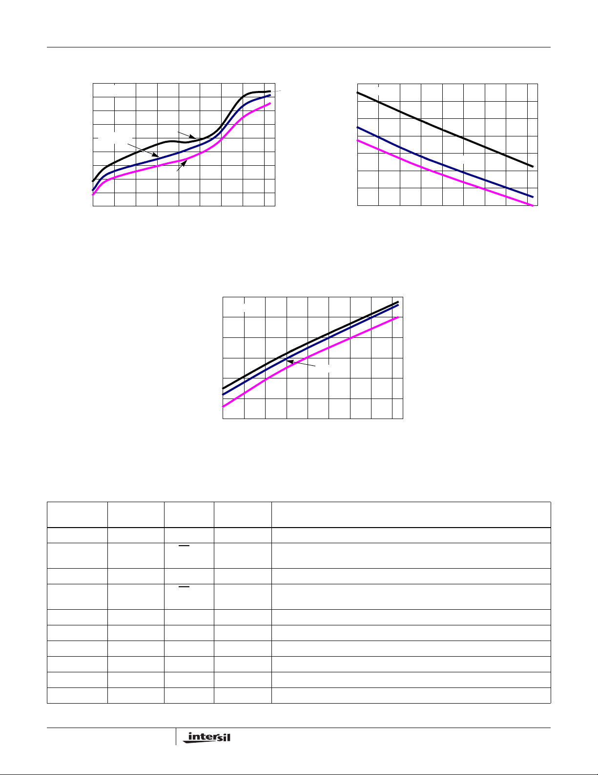
ISL28288
(10 LD MSOP)
1 3 IN+_A Circuit 1 Amplifier A non-inverting input
2EN
3 13 V- Circuit 4 Negative power supply
4EN
5 5 IN+_B Circuit 1 Amplifier B non-inverting input
6 6 IN-_B Circuit 1 Amplifier B inverting input
7 7 OUT_B Circuit 3 Amplifier B output
8 4 V+ Circuit 4 Positive power supply
9 1 OUT_A Circuit 3 Amplifier A output
10 2 IN-_A Circuit 1 Amplifier A inverting input
ISL28488
(16 LD Q SOP) PIN NAME
_A Circuit 2 Amplifier A enable pin internal pull-down; Logic “1” selects the disabled state;
_B Circuit 2 Amplifier B enable pin with internal pull-down; Logic “1” selects the disabled state;
EQUIVALENT
CIRCUIT DESCRIPTION
Logic “0” selects the enabled state.
Logic “0” selects the enabled state.
MEDIAN
= -2.5V, RL = 10, V
IN
+, V-
= ±2.5V
9
FN6339.1
June 28, 2007
Page 10
Pin Descriptions (Continued)
ISL28288, ISL28488
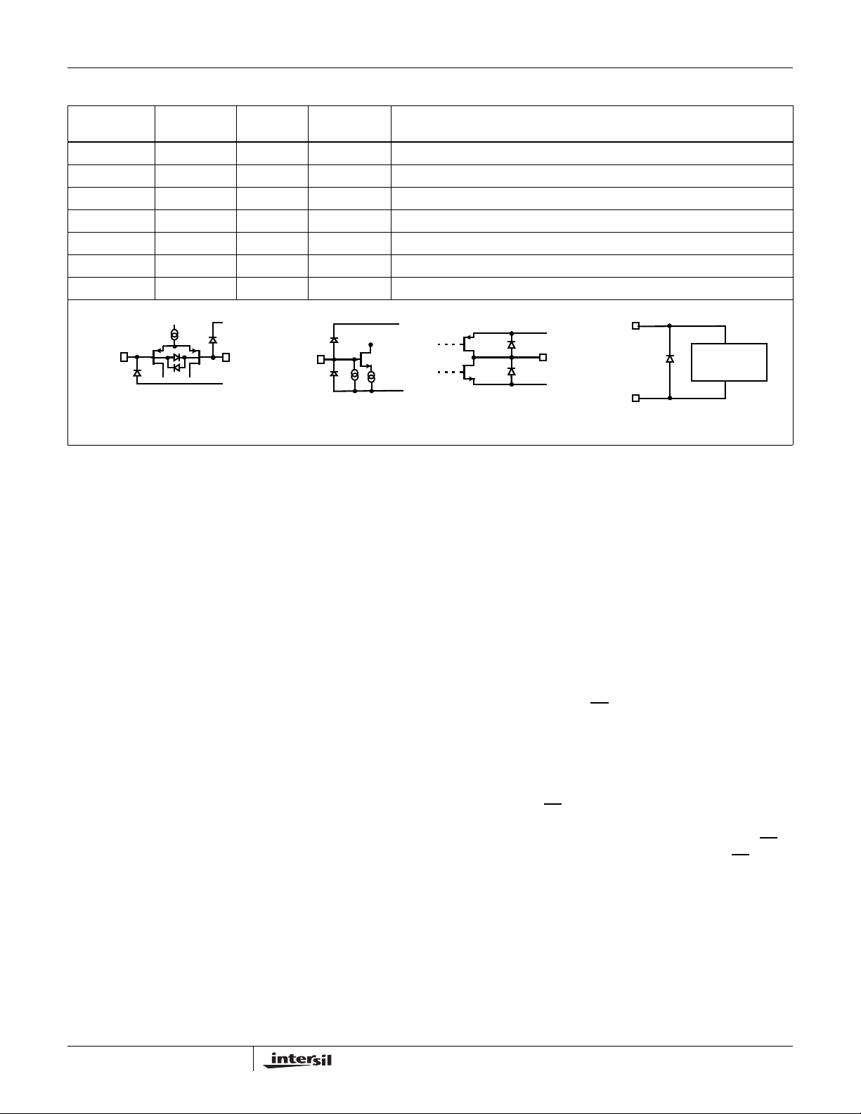
ISL28288
(10 LD MSOP)
IN-
ISL28488
(16 LD Q SOP) PIN NAME
10 OUT_C Circuit 3 Amplifier C output
11 IN-_C Circuit 1 Amplifier C inverting input
12 IN+_C Circuit 1 Amplifier C non-inverting input
14 IN+_D Circuit 1 Amplifier D non-inverting input
15 IN-_D Circuit 1 Amplifier D inverting input
16 OUT_D Circuit 3 Amplifier D output
8, 9 NC - No internal connection
V+
IN+
V-
CIRCUIT 1
EQUIVALENT
CIRCUIT DESCRIPTION
LOGIC
PIN
CIRCUIT 2
Applications Information
Introduction
The ISL28288 and ISL28488 are dual and quad CMOS
rail-to-rail input, output (RRIO) micropower operational
amplifiers. These devices are designed to operate from a
single supply (2.4V to 5.0V) or dual supplies (±1.2V to
±2.5V) while drawing only 120μA of supply current. This
combination of low power and precision performance makes
these devices suitable for solar and battery power
applications.
Rail-to-Rail Input
Many rail-to-rail input stages use two differential input pairs,
a long-tail PNP (or PFET) and an NPN (or NFET). Severe
penalties have to be paid for this circuit topology. As the
input signal moves from one supply rail to another, the
operational amplifier switches from one input pair to the
other causing drastic changes in input offset voltage and an
undesired change in magnitude and polarity of input offset
current.
The ISL28288 achieves input rail-to-rail without sacrificing
important precision specifications and degrading distortion
performance. The devices’ input offset voltage exhibits a
smooth behavior throughout the entire common-mode input
range. The input bias current versus the common-mode
voltage range gives us an undistorted behavior from typically
100mV below the negative rail and 10% higher than the V+
rail (0.5V higher than V+ when V+ equals 5V).
Input Protection
All input terminals have internal ESD protection diodes to both
positive and negative supply rails, limiting the input volt age to
V+
V-
V+
OUT
V-
CIRCUIT 3
V+
V-
CIRCUIT 4
CAPACITIVELY
COUPLED
ESD CLAMP
within one diode beyond the supply rails. There is an
additional pair of back-to-back diodes across the input
terminals. For applications where the input differential voltage
is expected to exceed 0.5V, external series resistors must be
used to ensure the input currents never exceed 5mA.
Rail-to-Rail Output
A pair of complementary MOSFET devices are used to achieve
the rail-to-rail output swing. The NMOS sinks current to swing
the output in the negative direction. The PMOS sources current
to swing the output in the positive direction. The ISL28288 with
a 100kΩ load will swing to within 4mV of the positive supply rail
and within 3mV of the negative supply rail.
Enable/Disable Feature
The ISL28288 offers an EN pin that disables the device
when pulled up to at least 2.0V. In the disabled state (output
in a high impedance state), the part consumes typically 4µA.
By disabling the part, multiple ISL28288 parts can be
connected together as a MUX. In this configuration, the
outputs are tied together in parallel and a channel can be
selected by the EN
pin. The loading effects of the feedback
resistors of the disabled amplifier must be considered when
multiple amplifier outputs are connected together. The EN
pin also has an internal pull down. If left open, the EN
pin will
pull to the negative rail and the device will be enabled by
default.
Using Only One Channel
The ISL28288 is a dual op amp. If the application only
requires one channel, the user must configure the unused
channel to prevent it from oscillating. The unused channel
will oscillate if the input and output pins are floating. This will
result in higher than expected supply currents and possible
10
FN6339.1
June 28, 2007
Page 11
ISL28288, ISL28488
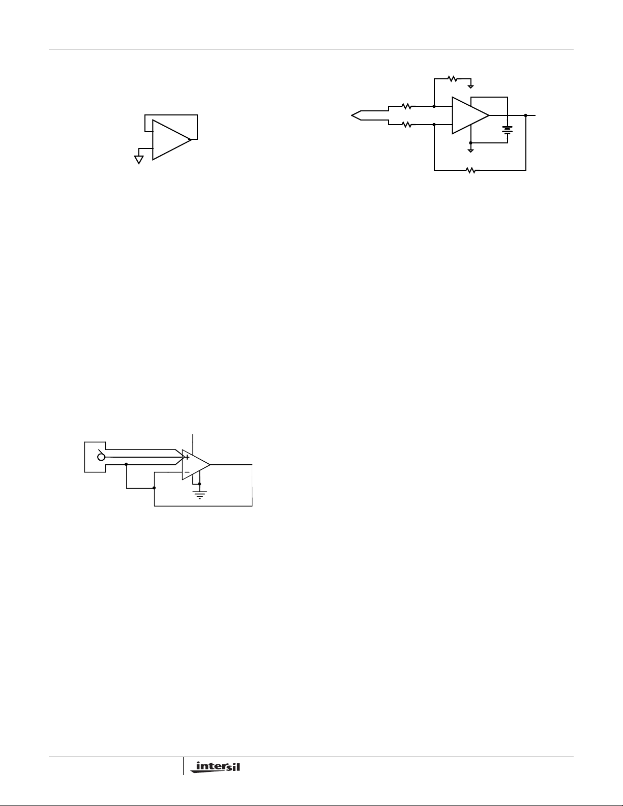
noise injection into the channel being used. The proper wa y
to prevent this oscillation is to short the output to the
negative input and ground the positive input (as shown in
Figure 34).
ISL28288
+
FIGURE 34. PREVENTING OSCILLATIONS IN UNUSED
CHANNELS
Proper Layout Maximizes Performance
To achieve the maximum performance of the high input
impedance and low offset voltage of the ISL28288, care
should be taken in the circuit board layout. The PC board
surface must remain clean and free of moisture to avoid
leakage currents between adjacent traces. Surface coating
of the circuit board will reduce surface moisture and provide
a humidity barrier, reducing parasitic resistance on the
board. When input leakage current is a concern, the use of
guard rings around the amplifier inputs will further reduce
leakage currents. Figure 35 shows a guard ring example for
a unity gain amplifier that uses the low impedance amplifier
output at the same voltage as the high impedance input to
eliminate surface leakage. The guard ring does not need to
be a specific width, but it should form a continuous loop
around both inputs. For further reduction of leakage
currents, components can be mounted to the PC board
using Teflon standoff insulators.
HIGH IMPEDANCE INPUT
IN
FIGURE 35. GUARD RING EXAMPLE FOR UNITY GAIN
AMPLIFIER
V+
Example Application
Thermocouples are the most popular temperature-sensing
device because of their low cost, interchangeability, and
ability to measure a wide range of temperatures. The
ISL28288 (Figure 36) is used to convert the differential
thermocouple voltage into single-ended signal with 10X gain.
The ISL28288's rail-to-rail input characteristic allows th e
thermocouple to be biased at ground and the amplifier to run
from a single 5V supply.
.
K TYPE
THERMOCOUPLE
FIGURE 36. THERMOCOUPLE AMPLIFIER
10kΩR
3
10kΩR
2
R
4
100kΩ
+
ISL28X88
-
V+
V-
R
1
100kΩ
+
410µV/°C
5V
Current Limiting
The ISL28288 has no internal current-limiting circuitry. If the
output is shorted, it is possible to exceed the Absolute
Maximum Rating for output current or power dissipation,
potentially resulting in the destruction of the device.
Power Dissipation
It is possible to exceed the +150°C maximum junction
temperatures under certain load and power-supply
conditions. It is therefore important to calculate the
maximum junction temperature (T
to determine if power supply voltages, load conditions, or
package type need to be modified to remain in the safe
operating area. These parameters are related in Equation 1:
T
JMAXTMAXθJA
xPD
()+=
MAXTOTAL
where:
•P
DMAXTOTAL
is the sum of the maximum power
dissipation of each amplifier in the package (PD
•PD
PD
for each amplifier is calculated in Equation 2:
MAX
MAX
2*VSI
( - V
SMAXVS
where:
•T
• θ
•PD
•V
•I
•V
= Maximum ambient temperature
MAX
= Thermal resistance of the package
JA
= Maximum power dissipation of 1 amplifier
MAX
= Supply voltage (Magnitude of V+ and V-)
S
= Maximum supply current of 1 amplifier
MAX
OUTMAX
= Maximum output voltage swing of the
application
•R
= Load resistance
L
) for all applications
JMAX
V
----------------------------
)
OUTMAX
×+×=
MAX
OUTMAX
R
L
(EQ. 1)
)
(EQ. 2)
11
FN6339.1
June 28, 2007
Page 12
ISL28288, ISL28488
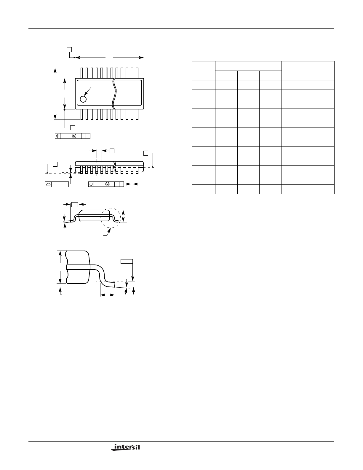
Quarter Size Outline Plastic Packages Family (QSOP)
E E1
0.010 C A B
C
SEATING
PLANE
0.004 C
A
N
PIN #1
I.D. MARK
1
B
L1
c
SEE DETAI L "X"
D
e
0.007 C A B
(N/2)+1
A
(N/2)
MDP0040
QUARTER SIZE OUTLINE PLASTIC PACKAGES FAMILY
INCHES
SYMBOL
A 0.068 0.068 0.068 Max. A1 0.006 0.006 0.006 ±0.002 A2 0.056 0.056 0.056 ±0.004 -
b 0.010 0.010 0.010 ±0.002 -
c 0.008 0.008 0.008 ±0.001 -
D 0.193 0.341 0.39 0 ±0.004 1, 3
E 0.236 0.236 0.236 ±0.008 -
H
E1 0.154 0.154 0.154 ±0.004 2, 3
e 0.025 0.025 0.025 Basic -
L 0.025 0.025 0.025 ±0.009 -
b
L1 0.041 0.041 0.041 Basic -
N 16 24 28 Reference -
NOTES:
1. Plastic or metal protrusions of 0.006” maximum per side are not
included.
2. Plastic interlead protrusions of 0.010” maximum per side are not
included.
3. Dimensions “D” and “E1” are measured at Datum Plane “H”.
4. Dimensioning and tolerancing per ASME Y14.5M-1994.
TOLERANCE NOTESQSOP16 QSOP24 QSOP28
Rev. F 2/07
A2
A1
DETAIL X
GAUGE
PLANE
L
0.010
4°±4°
12
FN6339.1
June 28, 2007
Page 13
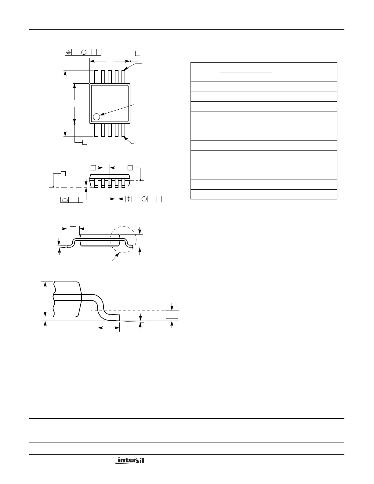
Mini SO Package Family (MSOP)
M
C
SEATING
PLANE
0.10 C
N LEADS
c
0.25 C A B
E1E
B
e
L1
SEE DETAIL "X"
D
N
1
b
A
(N/2)+1
PIN #1
I.D.
(N/2)
H
M
0.08 C A B
A
ISL28288, ISL28488
MDP0043
MINI SO PACKAGE FAMILY
SYMBOL
A1.101.10 Max. A1 0.10 0.10 ±0.05 A2 0.86 0.86 ±0.09 -
b 0.33 0.23 +0.07/-0.08 -
c0.180.18 ±0.05 D 3.00 3.00 ±0.10 1, 3
E4.904.90 ±0.15 -
E1 3.00 3.00 ±0.10 2, 3
e0.650.50 Basic -
L0.550.55 ±0.15 -
L1 0.95 0.95 Basic -
N 8 10 Reference -
NOTES:
1. Plastic or metal protrusions of 0.15mm maximum per side are not
included.
2. Plastic interlead protrusions of 0.25mm maximum per side are
not included.
3. Dimensions “D” and “E1” are measured at Datum Plane “H”.
4. Dimensioning and tolerancing per ASME Y14.5M-1994.
MILLIMETERS
TOLERANCE NOTESMSOP8 MSOP10
Rev. D 2/07
A2
GAUGE
A1
L
DETAIL X
PLANE
3° ±3°
0.25
All Intersil U.S. products are manufactured, assembled and tested utilizing ISO9000 quality systems.
Intersil Corporation’s quality certifications can be viewed at www.intersil.com/design/quality
Intersil products are sold by description only. Intersil Corporation reserves the right to make changes in circuit design, software and/or specifications at any time without
notice. Accordingly, the reader is cautioned to verify that data sheets are current before placing orders. Information furnished by Intersil is believed to be accurate and
reliable. However, no responsibility is assumed by Intersil or its subsidiaries for its use; nor for any infringements of patents or other rights of third parties which may result
from its use. No license is granted by implicat ion or oth erwise u nde r any p a tent or p at ent r ights of Intersil or its subsidiari es.
For information regarding Intersil Corporation and its products, see www.intersil.com
13
FN6339.1
June 28, 2007
 Loading...