

Page 1
®
Dual Digitally Controlled Potentiometer (XDCP™)
ISL22426
Data Sheet July 17, 2006
Low Noise, Low Power, SPI® Bus, 128 Taps
The ISL22426 integrates two digitally controlled
potentiometers (DCP) and non-volatile memory on a
monolithic CMOS integrated circuit.
The digitally controlled potentiometers are implemented with
a combination of resistor elements and CMOS switches. The
position of the wipers are controlled by the user through the
SPI serial interface. Each potentiometer has an associated
volatile Wiper Register (WR) and a non-volatile Initial Value
Register (IVR) that can be directly written to and read by the
user. The contents of the WR controls the position of the
wiper. At power-up the device recalls the contents of the
DCP’s IVR to the corresponding WR.
The DCPs can be used as three-terminal potentiometers or
as two-terminal variable resistors in a wide variety of
applications including control, parameter adjustments, and
signal processing.
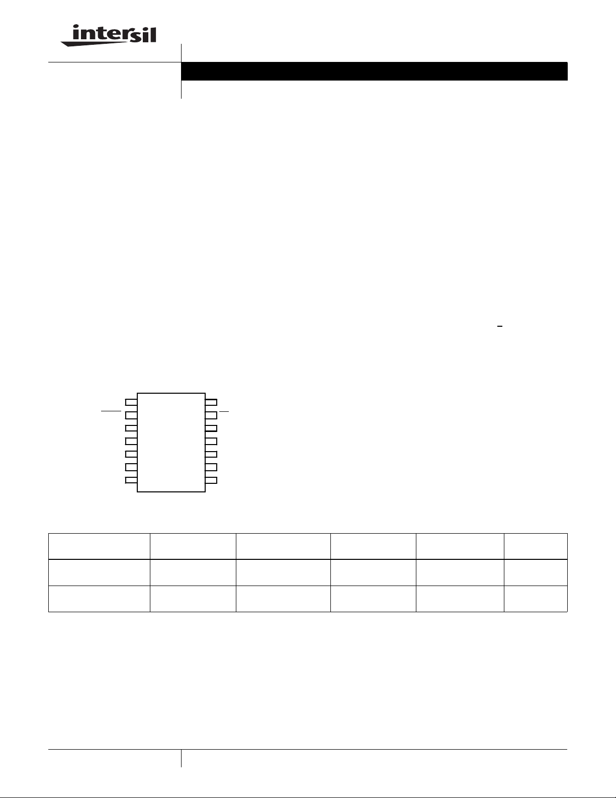
Pinout
ISL22426
(14 LEAD TSSOP)
TOP VIEW
14
CC
SHDN
RH0
RL0
RW0
NC
1
2
3
4
5
6
7
SDIV
CS
13
RH1
12
11
RL1
RW1
10
9
GND
SDOSCK 8
FN6180.0
Features
• Two potentiometers in one package
• 128 resistor taps
• SPI serial interface
• Non-volatile storage of wiper position
• Wiper resistance: 70Ω typical @ 3.3V
• Shutdown mode
• Shutdown current 5µA max
• Power supply: 2.7V to 5.5V
•50kΩ or 10kΩ total resistance
• High reliability
- Endurance: 1,000,000 data changes per bit per register
- Register data retention: 50 years @ T <
• 14 Lead TSSOP
• Pb-free plus anneal product (RoHS compliant)
55°C
Ordering Information
RESISTANCE OPTION
PART NUMBER PART MARKING
ISL22426UFV14Z
(Notes 1, 2)
ISL22426WFV14Z
(Notes 1, 2)
NOTES:
1. Intersil Pb-free plus anneal products employ special Pb-free material sets; molding compounds/die attach materials and 100% matte tin plate
termination finish, which are RoHS compliant and compatible with both SnPb and Pb-free soldering operations. Intersil Pb-free products are
MSL classified at Pb-free peak reflow temperatures that meet or exceed the Pb-free requirements of IPC/JEDEC J STD-020.
2. Add “-TK” suffix for 1,000 Tape and Reel option
22426 UFVZ 50 -40 to +125 14 Ld TSSOP
22426 WFVZ 10 -40 to +125 14 Ld TSSOP
1
1-888-INTERSIL or 1-888-468-3774
(kΩ)
CAUTION: These devices are sensitive to electrostatic discharge; follow proper IC Handling Procedures.
TEMP. RANGE
(°C) PACKAGE PKG. DWG. #
(Pb-free)
(Pb-free)
| Intersil (and design) and XDCP are registered trademarks of Intersil Americas Inc.
All other trademarks mentioned are the property of their respective owners.
Copyright Intersil Americas Inc. 2005. All Rights Reserved
M14.173
M14.173
Page 2
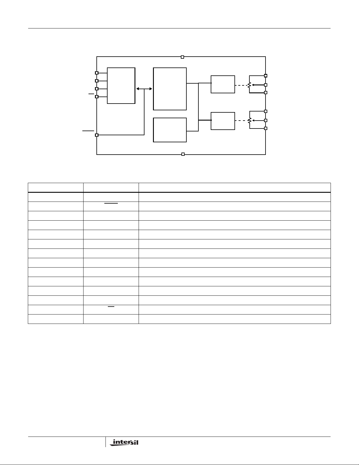
Block Diagram
ISL22426
V
CC
SCK
SDI
SDO
CS
SHDN
SPI
INTERFACE
POWER UP
INTERFACE,
CONTROL
AND STA TUS
LOGIC
NON-
VOLATILE
REGISTERS
GND
Pin Descriptions
TSSOP PIN SYMBOL DESCRIPTION
1V
CC
2SHDNShutdown active low input
3 RH0 “High” terminal of DCP0
4 RL0 “Low” terminal of DCP0
5 RW0 “Wiper” terminal of DCP0
6NC
7 SCK SPI interface clock input
8 SDO Open drain SPI interface Data Output
9 GND Device ground pin
10 RW1 “Wiper” terminal of DCP1
11 RL1 “Low” terminal of DCP1
12 RH1 “High” terminal of DCP1
13 CS
14 SDI SPI interface Data Input
Power supply pin
Chip Select active low input
WR1
WR0
RH1
RW1
RL1
RH0
RW0
RL0
2
FN6180.0
July 17, 2006
Page 3
ISL22426
Absolute Maximum Ratings Thermal Information
Storage Temperature. . . . . . . . . . . . . . . . . . . . . . . .-65°C to +150°C
Voltage at any Digital Interface Pin
with Respect to GND . . . . . . . . . . . . . . . . . . . . . -0.3V to V
V
. . . . . . . . . . . . . . . . . . . . . . . . . . . . . . . . . . . . . . . .-0.3V to +6V
CC
Voltage at any DCP pin with Respect to GND. . . . . . . -0.3V to V
Lead Temperature (Soldering, 10s) . . . . . . . . . . . . . . . . . . . . .300°C
I
(10s) . . . . . . . . . . . . . . . . . . . . . . . . . . . . . . . . . . . . . . . . . . ±6mA
W
Latchup (Note 4) . . . . . . . . . . . . . . . . . . Class II, Level B @ +125°C
CC
+0.3
CC
ESD (HBM) . . . . . . . . . . . . . . . . . . . . . . . . . . . . . . . . . . . . . . . 2.5kV
(CDM) . . . . . . . . . . . . . . . . . . . . . . . . . . . . . . . . . . . . . . . . .1kV
CAUTION: Stresses above those listed in “Absolute Maximum Ratings” may cause permanent damage to the device. This is a stress only rating and operation of the
device at these or any other conditions above those indicated in the operational sections of this specification is not implied.
NOTE:
θ
is measured with the component mounted on a high effective thermal conductivity test board in free air. See Tech Brief TB379 for details.
3.
JA
4. Jedec Class II pulse conditions and failure criterion used. Level B exceptions are: using a max positive pulse of 6.5V on the SHDN pin, and using
a max negative pulse of -0.8V for all pins.
Analog Specifications Over recommended operating conditions unless otherwise stated.
SYMBOL PARAMETER TEST CONDITIONS MIN
R
TOTALRH
to RL resistance W option 10 kΩ
U option 50 kΩ
R
to RL resistance tolerance W and U option -20 +20 %
H
End-to-End Temperature Coefficient W option ±50 ppm/°C
U option ±80 ppm/°C
V
, VRLVRH and VRL Terminal Voltages VRH and VRL to GND 0 V
RH
R
C
H/CL/CW
(Note 21)
I
LkgDCP
VOLTAGE DIVIDER MODE (0V @ R
INL
Wiper resistance VCC = 3.3V @ +25°C, wiper current =
W
Potentiometer capacitance
Leakage on DCP pins
i; VCC @ RHi; measured at RWi, unloaded; i = 0 or 1)
L
V
CC/RTOTAL
Voltage at pin from GND to V
Integral non-linearity Monotonic over all tap positions -1 1 LSB
(Note 10)
DNL
Differential non-linearity Monotonic over all tap positions -0.5 0.5 LSB
(Note 9)
ZSerror
(Note 7)
FSerror
(Note 8)
V
MATCH
(Note 11)
TC
(Note 12)
Zero-scale error W option 0 1 5 LSB
U option 0 0.5 2
Full-scale error W option -5 -1 0 LSB
U option -2 -1 0
DCP to DCP matching Any two DCPs at same tap position, same
voltage at all RH terminals, and same voltage
at all R
terminals
L
Ratiometric temperature coefficient DCP register set to 40 hex ±4 ppm/°C
V
Thermal Resistance (Typical, Note 3)
θ
JA
(°C/W)
14 Lead TSSOP. . . . . . . . . . . . . . . . . . . . . . . . . . . . 100
Recommended Operating Conditions
Temperature Range (Extended Industrial). . . . . . . .-40°C to +125°C
Power Rating . . . . . . . . . . . . . . . . . . . . . . . . . . . . . . . . . . . . . .5mW
Maximum Junction Temperature . . . . . . . . . . . . . . . . . . . . . .+150°C
V
. . . . . . . . . . . . . . . . . . . . . . . . . . . . . . . . . . . . . . . . 2.7V to 5.5V
CC
Wiper Current . . . . . . . . . . . . . . . . . . . . . . . . . . . . . . . . . . . .±3.0mA
TYP
(NOTE 5) MAX UNIT
(Note 21)
(Note 21)
V
(Note 6)
(Note 6)
(Note 6)
(Note 6)
(Note 6)
CC
CC
70 200 Ω
10/10/25 pF
0.1 1 µA
-2 2 LSB
3
FN6180.0
July 17, 2006
Page 4
ISL22426
Analog Specifications Over recommended operating conditions unless otherwise stated. (Continued)
SYMBOL PARAMETER TEST CONDITIONS MIN
RESISTOR MODE (Measurements between RWi and RLi with RHi not connected, or between RWi and RHi with RLi not connected; i = 0 or 1)
RINL
(Note 16)
RDNL
(Note 15)
Roffset
Integral non-linearity DCP register set between 10h and 7Fh;
-1 1 MI
monotonic over all tap positions
Differential non-linearity DCP register set between 10h and 7Fh;
-0.5 0.5 MI
monotonic over all tap positions
Offset W option 0 1 7 MI
(Note 14)
U option 0 0.5 2 MI
R
MATCH
(Note 17)
DCP to DCP matching Any two DCPs at the same tap position with
the same terminal voltages
-2 2 MI
Operating Specifications Over the recommended operating conditions unless otherwise specified.
SYMBOL PARAMETER TEST CONDITIONS MIN
I
CC1
I
CC2
I
SB
I
SD
I
LkgDig
t
WRT
(Note 21)
t
ShdnRec
VCC supply current (volatile
write/read)
VCC supply current (non-volatile
write/read)
VCC current (standby) V
VCC current (shutdown) V
Leakage current, at pins SHDN, SCK,
SDI, SDO and CS
Wiper Response Time after SPI write
to WR register
DCP recall time from shutdown mode From rising edge of SHDN
(Note 21)
Vpor Power-on recall voltage Minimum V
VccRamp V
t
D
ramp rate 0.2 V/ms
CC
Power-up delay VCC above Vpor, to DCP Initial Value
f
= 5MHz; (for SPI Active, Read and
SCK
Volatile Write states only)
f
= 5MHz; (for SPI Active, Read and Non-
SCK
volatile Write states only)
= +5.5V @ +85°C, SPI interface in
CC
standby state
V
= +5.5V @ +125°C, SPI interface in
CC
standby state
V
= +3.6V @ +85°C, SPI interface in
CC
standby state
= +3.6V @ +125°C, SPI interface in
V
CC
standby state
= +5.5V @ +85°C, SPI interface in
CC
standby state
V
= +5.5V @ +125°C, SPI interface in
CC
standby state
= +3.6V @ +85°C, SPI interface in
V
CC
standby state
V
= +3.6V @ +125°C, SPI interface in
CC
standby state
Voltage at pin from GND to V
CC
signal to wiper
stored position and RH connection
SCK rising edge of last bit of ACR data byte
to wiper stored position and RH connection
at which memory recall occurs 2.0 2.6 V
CC
Register recall completed, and SPI Interface
in standby state
-1 1 µA
TYP
(NOTE 5) MAX UNIT
(Note 13)
(Note 13)
(Note 13)
(Note 13)
(Note 13)
TYP
(NOTE 5) MAX UNIT
0.5 mA
3mA
5µA
7µA
3µA
5µA
3µA
5µA
2µA
4µA
1.5 µs
1.5 µs
1.5 µs
3ms
4
FN6180.0
July 17, 2006
Page 5
ISL22426
Operating Specifications Over the recommended operating conditions unless otherwise specified. (Continued)
SYMBOL PARAMETER TEST CONDITIONS MIN
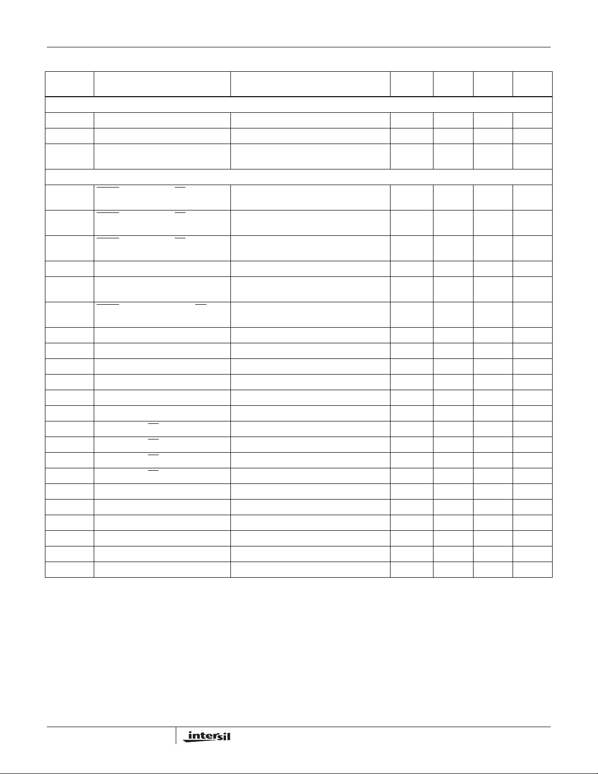
EEPROM SPECIFICATION
EEPROM Endurance 1,000,000 Cycles
t
WC
EEPROM Retention Temperature °C 50 Years
Non-volatile Write cycle time 12 20 ms
T55≤
(Note 19)
SERIAL INTERFACE SPECIFICATIONS
V
SHDN, SCK, SDI, and CS input buffer
IL
-0.3 0.3*V
LOW voltage
V
Hysteresis
V
R
(Note 20)
Cpin
(Note 21)
f
SCK
t
CYC
t
WH
t
WL
t
LEAD
t
LAG
t
SU
t
t
t
t
DIS
t
t
HO
t
RO
t
FO
t
CS
SHDN, SCK, SDI, and CS input buffer
IH
HIGH voltage
SHDN, SCK, SDI, and CS input buffer
hysteresis
SDO output buffer LOW voltage IOL = 4mA 0 0.4 V
OL
SDO pull-up resistor off-chip Maximum is determined by t
pu
SHDN
, SCK, SDI, SDO and CS pin
maximum bus load Cb = 30pF, f
and tFO with
RO
= 5MHz
SCK
0.7*V
0.05*
V
CC
capacitance
SPI frequency 5MHz
SPI clock cycle time 200 ns
SPI clock high time 100 ns
SPI clock low time 100 ns
Lead time 250 ns
Lag time 250 ns
SDI, SCK and CS input setup time 50 ns
SDI, SCK and CS input hold time 50 ns
H
SDI, SCK and CS input rise time 10 ns
RI
SDI, SCK and CS input fall time 10 20 ns
FI
SDO output Disable time 0 100 ns
SDO output valid time 350 ns
V
SDO output hold time 0 ns
SDO output rise time Rpu = 2k, Cb = 30pF 60 ns
SDO output fall time Rpu = 2k, Cb = 30pF 60 ns
CS deselect time 2µs
NOTES:
5. Typical values are for T
6. LSB: [V(R
incremental voltage when changing from one tap to an adjacent tap.
– V(RW)0]/127. V(RW)
W)127
7. ZS error = V(RW)
8. FS error = [V(RW)
9. DNL = [V(RW)
10. INL = [V(RW)
11. V
MATCH
12. for i = 16 to 112 decimal, T = -40°C to +125°C. Max( ) is the maximum value of the wiper
TC
V
– V(RW)
i
– i • LSB – V(RW)]/LSB for i = 1 to 127
i
= [V(RWx)i – V(RWy)i]/LSB, for i = 1 to 127, x = 0 or 1 and y = 0 or 1.
Max V RW()
()Min V RW()
----------------------------------------------------------------------------------------------
()Min V RW()
Max V RW()
= +25°C and 3.3V supply voltage.
A
and V(RW)0 are V(RW) for the DCP register set to 7F hex and 00 hex respectively. LSB is the
127
/LSB.
0
– VCC]/LSB.
127
]/LSB-1, for i = 1 to 127. i is the DCP register setting.
i-1
()–
i
i
()+[]2⁄
i
i
---------------- -
×=
165°C
6
10
voltage and Min ( ) is the minimum value of the wiper voltage over the temperature range.
TYP
(NOTE 5) MAX UNIT
CC
VCC+0.3 V
2kΩ
10 pF
CC
V
V
5
FN6180.0
July 17, 2006
Page 6
ISL22426
13. MI = |RW
00 hex respectively.
14. Roffset = RW
Roffset = RW
15. RDNL = (RW
16. RINL = [RW
17. R
MATCH
18. for i = 16 to 1 12, T = -40°C to +125°C. Max( ) is the maximum value of the resistance and Min ( ) is
TC
R
is the time from the end of a Write sequence of SPI serial interface, to the end of the self-timed internal non-volatile write cycle.
19. t
WC
– RW
127
= (RW
Max Ri()Min Ri()–[]
--------------------------------------------------------------- -
Max Ri()Min Ri()+[]2⁄
|/127. MI is a minimum increment. RW
0
/MI, when measuring between RW and RL.
0
/MI, when measuring between RW and RH.
127
– RW
i
– (MI • i) – RW0]/MI, for i = 1 to 127.
i
)/MI, for i = 1 to 127.
i-1
– RW
i,x
)/MI, for i = 1 to 127, x = 0 or 1 and y = 0 or 1.
i,y
---------------- -
×=
165°C
6
10
the minimum value of the resistance over the temperature range.
and RW0 are the measured resistances for the DCP register set to 7F hex and
127
20. Rpu is specified for the highest data rate transfer for the device. Higher value pull-up can be used at lower data rates.
21. This parameter is not 100% tested.
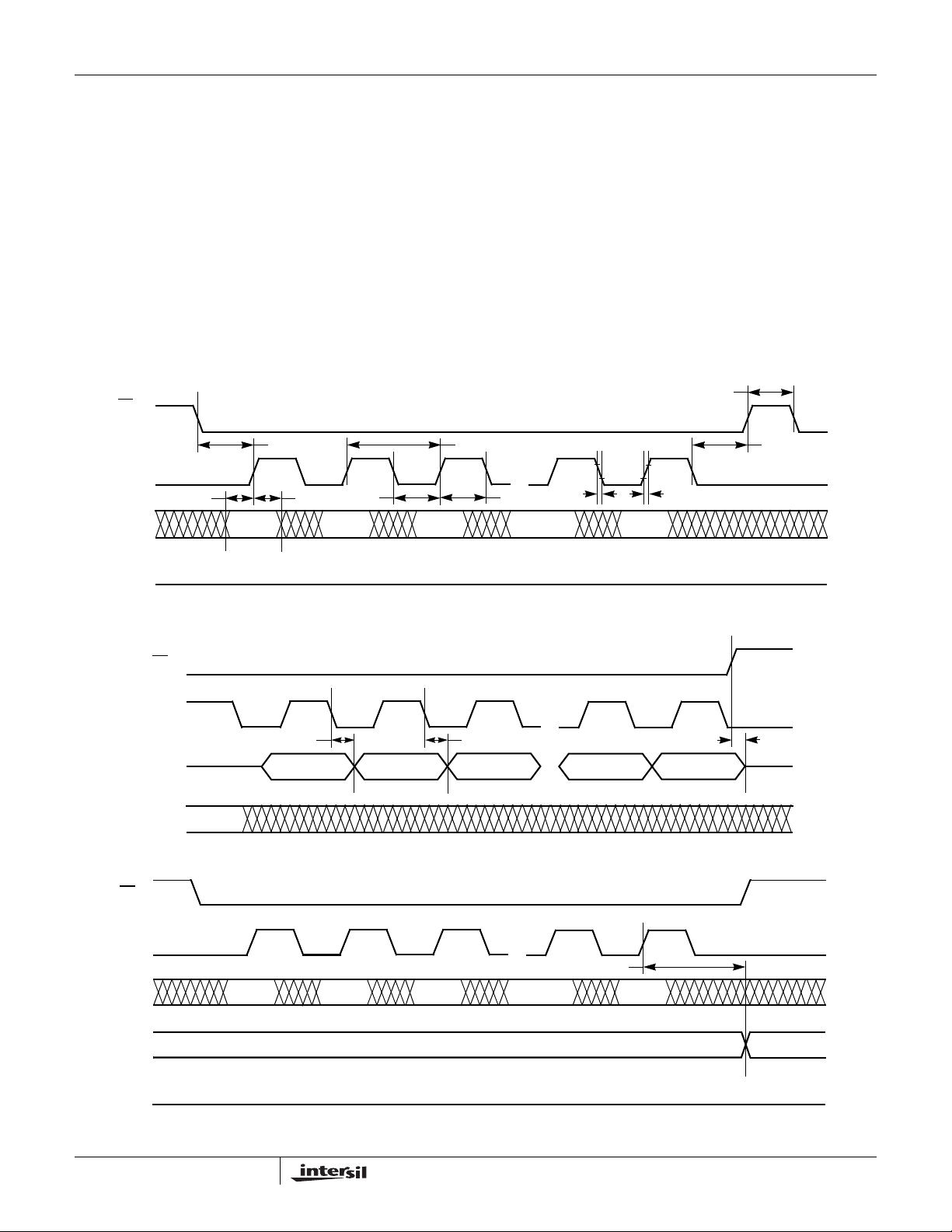
Timing Diagrams
Input Timing
t
CS
SCK
SDI
t
LEAD
t
CYC
...
t
SU
MSB LSB
t
H
t
WL
t
WH
...
t
FI
CS
t
LAG
t
RI
SDO
HIGH IMPEDANCE
Output Timing
CS
SCK
t
V
SDO
SDI
ADDR
MSB LSB
XDCP Timing (for All Load Instructions)
CS
SCK
SDI
MSB LSB
t
HO
t
DIS
...
...
...
t
WRT
...
V
SDO
W
HIGH IMPEDANCE
6
FN6180.0
July 17, 2006
Page 7
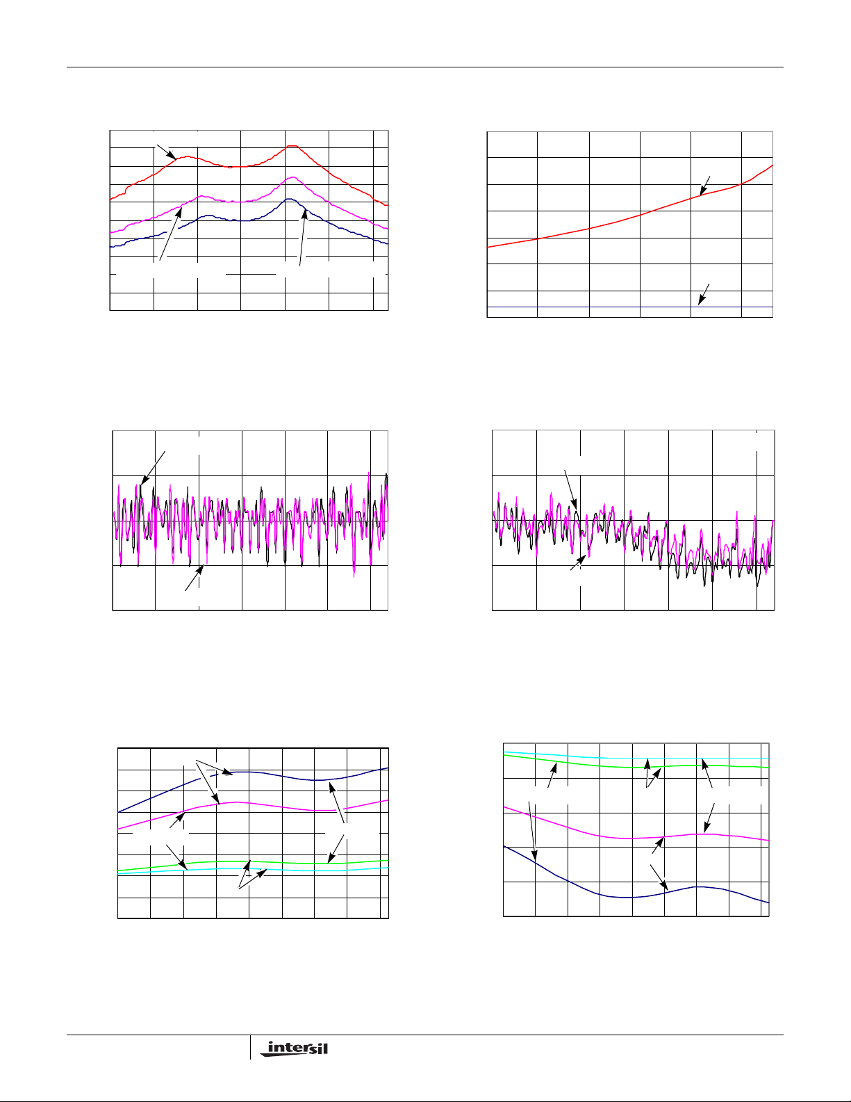
Typical Performance Curves
VCC
100
Vcc = 3.3V, T = 125ºC
90
80
70
60
50
40
30
Vcc = 3.3V, T = 20ºC
WIPER RESISITANCE (Ω)
20
10
0
0 20406080100120
TAP PO SITION ( D E C I MAL )
Vcc = 3.3V, T = -40º C
ISL22426
1.4
1.2
1
VCC
0.8
0.6
Isb (µA)
0.4
0.2
0
2.73.23.74.24.75.2
T = 1 25
T = 25
ºC
ºC
Vcc, V
FIGURE 1. WIPER RESISTANCE vs T AP POSITION
[ I(RW) = V
CC/RTOTAL
] FOR 10kΩ (W)
0.2
Vcc = 2.7V
T = 25ºC
0.1
0
DNL (LSB)
-0. 1
Vcc = 5.5V
-0. 2
0 20 40 60 80 100 120
TAP PO S I T I ON (D E C I MAL )
FIGURE 3. DNL vs TAP POSITION IN VOLTAGE DIVIDER
MODE FOR 10kΩ (W)
1.30
10k
1.10
0.90
0.70
0.50
0.30
ZSerror (LSB)
Vcc = 5.5 V
Vcc = 2.7 V
0.10
-0.10
50k
-0.30
-40 -20 0 20 40 60 80 100 120
TEMPERATURE (ºC)
FIGURE 2. STANDBY I
CC
vs V
CC
0.2
T = 25ºC
0.1
Vcc = 2.7 V
0
INL (LSB)
-0.1
Vcc = 5.5V
-0.2
0 20406080100120
TAP PO SITION ( D E C I MAL )
FIGURE 4. INL vs TAP POSITION IN VOL TAGE DIVIDER
MODE FOR 10kΩ (W)
0.00
-0. 30
Vcc = 2.7V Vcc = 5.5V
50k
-0. 60
-0. 90
FSerror (LSB)
10k
-1. 20
-1. 50
-40-200 20406080100120
TEMPERATURE (ºC)
FIGURE 5. ZSerror vs TEMPERATURE
7
FIGURE 6. FSerror vs TEMPERATURE
FN6180.0
July 17, 2006
Page 8
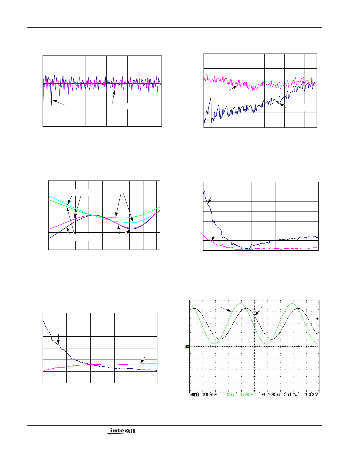
Typical Performance Curves (Continued)
V
C
V
ISL22426
0.4
T = 25º
0.2
0
-0 .2
DNL (LSB)
Vcc = 2.7
Vcc = 5.5
-0 .4
-0 .6
16 36 56 76 96 116
TAP PO S ITIO N (D EC IMAL)
FIGURE 7. DNL vs TAP POSITION IN Rheostat MODE FOR
10kΩ (W)
1.00
50k
0.50
CHANGE (%)
0.00
TOTAL
Vcc = 2.7V
0.4
T = 25ºC
0.2
0
Vcc = 5 .5 V
-0.2
INL (LSB)
Vcc = 2.7V
-0.4
-0.6
16 36 56 76 96 116
TAP POSI TI ON (DE CIMAL)
FIGURE 8. INL vs TAP POSITION IN Rheostat MODE FOR
10kΩ (W)
105
90
10k
75
60
45
-0.50
END TO END R
-1.00
Vcc = 5.5V
10k
-40 -20 0 20 40 60 80 100 120
TEMPERATURE (º C)
FIGURE 9. END TO END R
TEMPERATURE
300
250
200
150
TCr (ppm/°C)
100
50
10k
0
16 36 56 76 96
TAP PO S I TI O N (D E C I MAL)
FIGURE 11. TC FOR Rheostat MODE IN ppm
% CHANGE vs
TOTAL
50k
TCv (ppm/°C)
30
50k
15
0
16 36 56 76 96
TAP PO SI TION (DEC IMAL)
FIGURE 10. TC FOR VOLTAGE DIVIDER MODE IN ppm
INPUT
Wiper at Mid Point (position 40h)
Rtotal = 9.5kΩ
FIGURE 12. FREQUENCY RESPONSE (2.6MHz)
OUTPUT
8
FN6180.0
July 17, 2006
Page 9
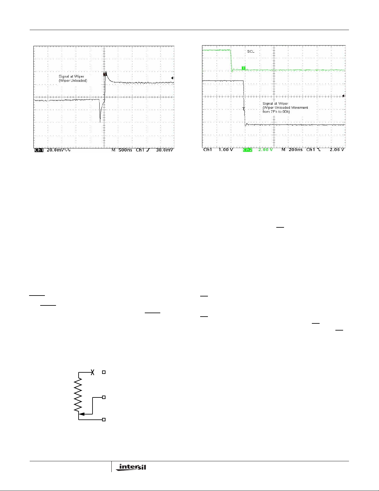
Typical Performance Curves (Continued)
Wiper Mid Point Movement
from 3Fh to 40h
ISL22426
FIGURE 13. MIDSCALE GLITCH, CODE 3Fh TO 40h
Pin Description
Potentiometer Pins
RHi and RLi (i = 0, 1)
The high (RHi) and low (RLi) terminals of the ISL22426 are
equivalent to the fixed terminals of a mechanical
potentiometer. RHi and RLi are referenced to the relative
position of the wiper and not the voltage potential on the
terminals. With WRi set to 127 decimal, the wiper will be
closest to RHi, and with the WRi set to 0, the wiper is closest
to RLi.
RWi (i = 0, 1)
RWi is the wiper terminal and is equivalent to the movable
terminal of a mechanical potentiometer. The position of the
wiper within the array is determined by the WRi register.
SHDN
The SHDN pin forces the resistor to end-to-end open circuit
condition on RHi and shorts RWi to RLi. When SHDN
returned to logic high, the previous latch settings put RWi at
the same resistance setting prior to shutdown. This pin is
logically ORed with SHDN bit in ACR register. SPI interface
is still available in shutdown mode and all registers are
accessible. This pin must remain HIGH for normal operation.
is
FIGURE 14. LARGE SIGNAL SETTLING TIME
Bus Interface Pins
Serial Clock (SCK)
This is the serial clock input of the SPI serial interface.
Serial Data Output (SDO)
The SDO is an open drain serial data ou tput pin. During a
read cycle, the data bits are shifted out at the falling edge of
the serial clock SCK, while the CS input is low.
SDO requires an external pull-up resistor for proper
operation.
Serial Data Input (SDI)
The SDI is the serial data input pin for the SPI interface. It
receives device address, operation code, wiper address and
data from the SPI external host device. The data bits are
shifted in at the rising edge of the serial clock SCK, while the
CS
input is low.
Chip Select (CS)
LOW enables the ISL22426, placing it in the active
CS
power mode. A HIGH to LOW transition on CS
prior to the start of any operation after power up. When CS
HIGH, the ISL22426 is deselected and the SDO pin is at
high impedance, and (unless an internal write cycle is
underway) the device will be in the standby state.
is required
is
RHi
RWi
RLi
FIGURE 15. DCP CONNECTION IN SHUTDOWN MODE
9
Principles of Operation
The ISL22426 is an integrated circuit incorporating two
DCPs with its associated registers, non-volatile memory and
the SPI serial interface providing direct communication
between host and potentiometers and memory. The resistor
array is comprised of individual resistors connected in
series. At either end of the array and between each resistor
is an electronic switch that transfers the potential at that
point to the wiper.
FN6180.0
July 17, 2006
Page 10

ISL22426
The electronic switches on the device operate in a “make
before break” mode when the wiper changes tap positions.
When the device is powered down, the last value stored in
IVRi will be maintained in the non-volatile memory. When
power is restored, the contents of the IVRi is recalled and
loaded into the corresponding WRi to set the wiper to the
initial value.
DCP Description
Each DCP is implemented with a combination of resistor
elements and CMOS switches. The physical ends of each
DCP are equivalent to the fixed terminals of a mechanical
potentiometer (RH and RL pins). The RW pin of each DCP is
connected to intermediate nodes, and is equivalent to the
wiper terminal of a mechanical potentiometer. The position
of the wiper terminal within the DCP is controlled by volatile
Wiper Register (WR). Each DCP has its own WR. When the
WR of a DCP contains all zeroes (WR[6:0]= 00h), its wiper
terminal (RW) is closest to its “Low” terminal (RL). When the
WR register of a DCP contains all ones (WR[6:0]= 7Fh), its
wiper terminal (RW) is closest to its “High” terminal (RH). As
the value of the WR increases from all zeroes (0) to all ones
(127 decimal), the wiper moves monotonically from the
position closest to RL to the closest to RH. At the same time,
the resistance between RW and RL increases monotonically,
while the resistance between RH and RW decreases
monotonically.
While the ISL22426 is being powered up, all four WRs are
reset to 40h (64 decimal), which locates RW roughly at the
center between RL and RH. After the power supply voltage
becomes large enough for reliable non-volatile memory
reading, all WRs will be reload with the value stored in
corresponding non-volatile Initial Value Registers (IVRs).
The WRs can be read or written to directly using the SPI
serial interface as described in the following sections. The
SPI interface register address bits have to be set to 0000b or
0001b to access the WR of DCP0 or DCP1 respectively. The
WRi and IVRi can be read or written to directly using the SPI
serial interface as described in the following sections.
Memory Description
The ISL22426 contains seven non-volatile and three volatile
8-bit registers. The memory map of ISL22426 is on Table 1.
The two non-volatile registers (IVRi) at address 0 and 1,
contain initial wiper value and volatile registers (WRi) contain
current wiper position. In addition, five non-volatile General
Purpose registers from address 2 to address 6 are available.
TABLE 1. MEMORY MAP
ADDRESS NON-VOLATILE VOLATILE
8— ACR
7 Reserved
TABLE 1. MEMORY MAP
ADDRESS NON-VOLATILE VOLATILE
6
5
4
3
2
1
0
General Purpose
General Purpose
General Purpose
General Purpose
General Purpose
IVR1
IVR0
Not Available
Not Available
Not Available
Not Available
Not Available
WR1
WR0
The non-volatile IVRi and volatile WRi registers are
accessible with the same address.
The Access Control Register (ACR) contains information
and control bits described below in Table 2.
The VOL bit (ACR[7]) determines whether the access is to
wiper registers WR or initial value registers IVR.
TABLE 2. ACCESS CONTROL REGISTER (ACR)
BIT #76543210
Bit Name VOL SHDN WIP
00000
If VOL bit is 0, the non-volatile IVR register is accessible. If
VOL bit is 1, only the volatile WR is accessible. Note, value
is written to IVR register also is written to the WR. The
default value of this bit is 0.
The SHDN bit (ACR[6]) disables or enables Shutdown
mode. This bit is logically ORed with SHDN
pin. When this
bit is 0, DCP is in Shutdown mode. The default value of
SHDN bit is 1.
The WIP bit (ACR[5]) is read only bit. It indicates that nonvolatile write operation is in progress. The WIP bit can be
read repeatedly after a non-volatile write to determine if the
write has been completed. It is impossible to write to the
IVRi, WRi or ACR while WIP bit is 1.
SPI Serial Interface
The ISL22426 supports an SPI serial protocol, mode 0. The
device is accessed via the SDI input and SDO output with
data clocked in on the rising edge of SCK, and clocked out
on the falling edge of SCK. CS
communication with the ISL22426. SCK and CS
controlled by the host or master. The ISL22426 operates
only as a slave device.
All communication over the SPI interface is conducted by
sending the MSB of each byte of data first.
must be LOW during
lines are
10
FN6180.0
July 17, 2006
Page 11
ISL22426
Protocol Conventions
The first byte sent to the ISL22426 from the SPI host is the
Identification Byte. A valid Identification Byte contains 0101
as the four MSBs, with the following four bits set to 0.
TABLE 3. IDENTIFICATION BYTE FORMAT
01010000
(MSB) (LSB)
The next byte sent to the ISL22426 contains the instruction
and register pointer information. The four MSBs are the
instruction and four LSBs are register address (see Table 4).
TABLE 4. IDENTIFICATION BYTE FORMAT
76543210
I3 I2 I1 I0 R3 R2 R1 R0
There are only two valid instruction sets:
1011(binary) - is a Read operation
1 100(binary) - is a Write operation
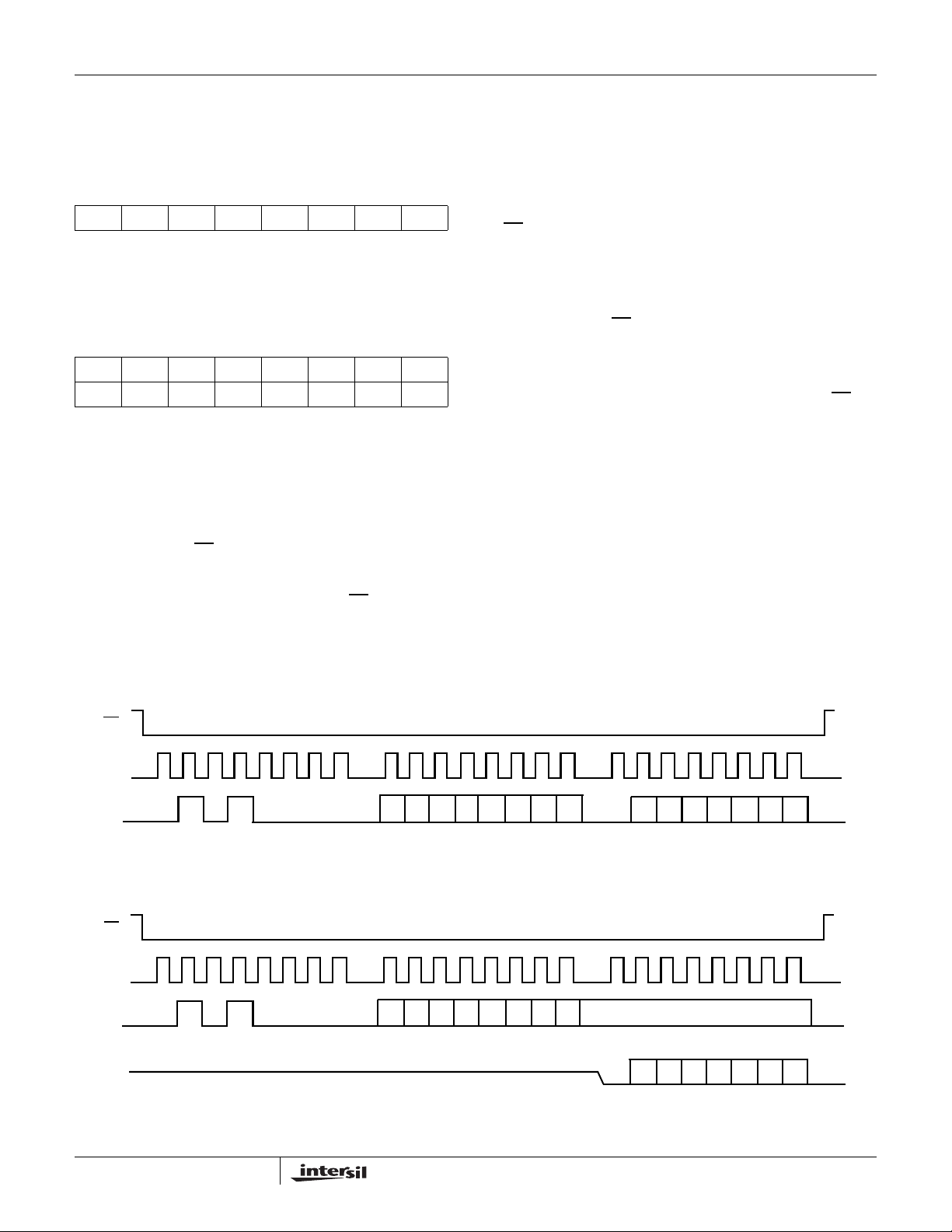
Write Operation
A Write operation to the ISL22426 is a three-byte operation.
It requires first, the CS transition from HIGH to LOW, then a
valid Identification Byte, then a valid instruction byte
following by Data Byte is sent to SDI pin. The host
terminates the write operation by pulling the CS
LOW to HIGH. For a write to addresses 0000b or 0001b, the
MSB at address 8 (ACR[7]) determines if the Data Byte is to
pin from
be written to volatile or both volatile and non-volatile
registers. Refer to “Memory Description” and Figure 16.
Device can receive more than one byte of data by auto
incrementing the address after each received byte. Note
after reaching the address 0110b, the internal pointer “rolls
over” to address 0000b.
The internal non-volatile write cycle starts after rising edge of
and takes up to 20ms. Thus, non-volatile registers must
CS
be written individually.
Read Operation
A read operation to the ISL22426 is a three-byte operation. It
requires first, the CS
valid Identification Byte, then a valid instruction byte
following by “dummy” Data Byte is sent to SDI pin. The SPI
host reads the data from SDO pin on falling edge of SCK.
The host terminates the read operation by pulling the CS
from LOW to HIGH (see Figure 17).
The ISL22426 will provide the Data Bytes to the SDO pin as
long as SCK is provided by the host from the registers
indicated by an internal pointer. This pointer initial value is
determined by the register address in the Read operation
instruction, and increments by one during transmission of
each Data Byte. After reaching the memory location 0110b,
the pointer “rolls over” to 0000b, and the device continues to
output the data for each received SCK clock.
In order to read back the non-volatile IVR, it is recommended
that the application reads the ACR first to verify the WIP bit
is 0. If the WIP bit (ACR[5]) is not 0, the host should repeat
its reading sequence again.
transition from HIGH to LOW, then a
pin
CS
SCK
SDI
CS
SCK
SDI
SDO
0 1 0 1 0 0 I3 I2 I1 I0 R3 R2 R1 R0
0101 00 I3 I2 I1 I0 R3 R2 R1 R0
00
00
0
FIGURE 16. THREE BYTE WRITE SEQUENCE
0
FIGURE 17. THREE BYTE READ SEQUENCE
11
0 D6D5D4 D3D2 D1D0
DON’T CARE
0 D6D5D4 D3D2 D1D0
FN6180.0
July 17, 2006
Page 12
A
xxxxxxx
x
ISL22426
Applications Information
any non-volatile memory changes. This is done by setting
MSB bit at address 1000b to 1.
Communicating with ISL22426
Communication with ISL22426 proceeds using SPI interface
through the ACR (address 1000b), IVRi (addresses 0000b,
0001b) and WRi (addresses 0000b, 0001b) registers.
The wiper of the potentiometer is controlled by the WRi
register. Writes and reads can be made directly to these
registers to control and monitor the wiper position without
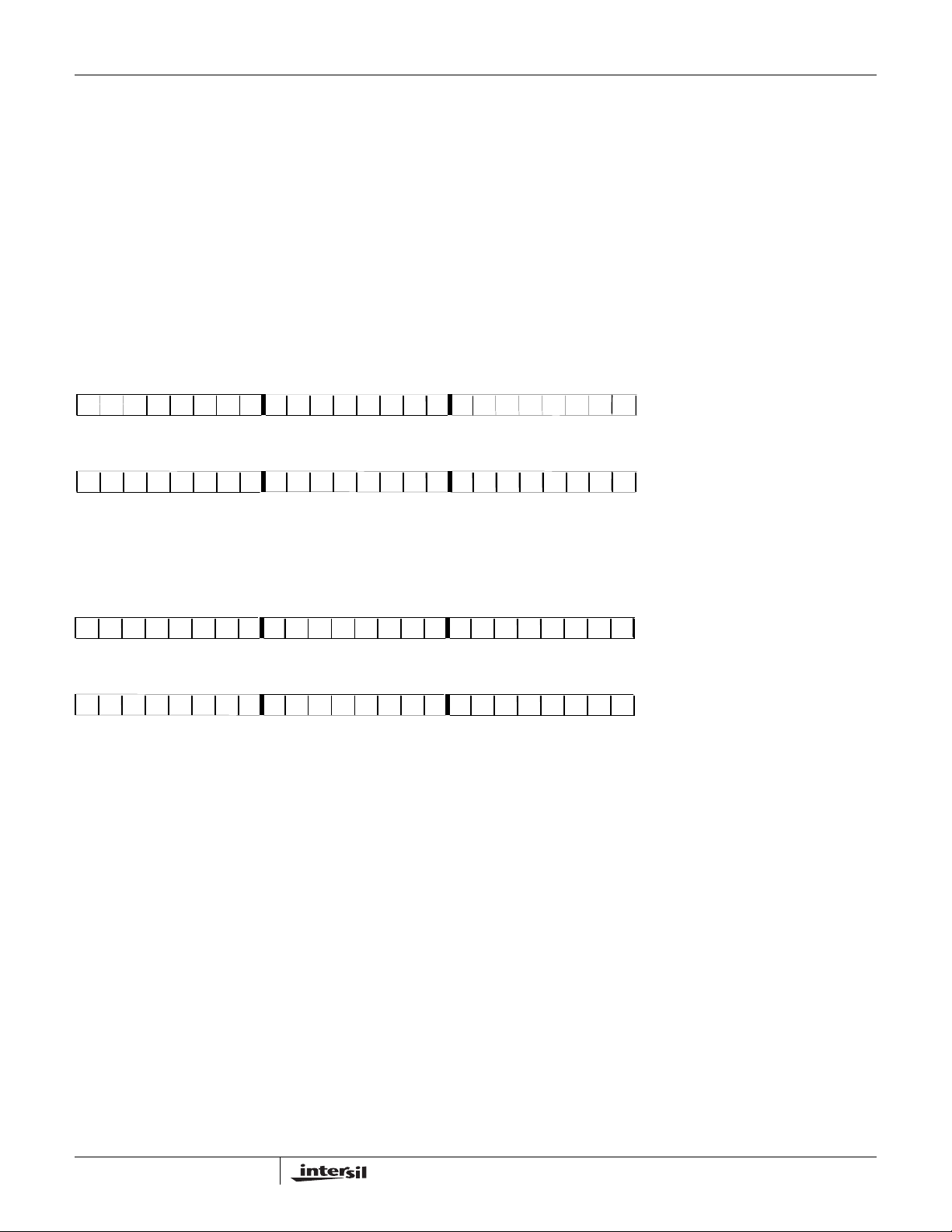
Examples:
Examples:
The non-volatile IVRi stores the power up value of the wiper.
IVRs are accessible when MSB bit at address 1000b is set
to 0. Writing a new value to the IVRi register will set a new
power up position for the wiper. Also, writing to this register
will load the same value into the corresponding WRi as the
IVRi. Reading from the IVRi will not change the WRi, if its
contents are different.
. Writing to the IVR:
This sequence will write a new value (77h) to the IVR0(non-volatile):
Set the ACR (Addr 1000b) for NV write (40h)
Send the ID byte, Instruction Byte, then the Data byte
0 1 0 1 0 0 0 0 1 1 0 0 1 00001000000
(Sent to DI)
Set the IVR0 (Addr 0000b) to 77h
Send the ID byte, Instruction Byte, then the Data byte
0 1 0 1 0 0 0 0 1 1 0 0 0 00001110111
(Sent to DI)
B. Reading from the WR:
This sequence will read the value from the WR1 (volatile):
Write to ACR first to access the volatile WRs
Send the ID byte, Instruction Byte, then the Data byte
0 1 0 1 0 0 0 0 1 1 0 0 1 0 0 0 1 1 0 0 0 0 0 0
(Sent to DI)
Read the data from WR1 (Addr 0001b)
Send the ID byte, Instruction Byte, then Read the Data byte
0 1 0 1 0 0 0 0 1 0 1 1 0 0 0 1
(Out on DO)
12
FN6180.0
July 17, 2006
Page 13
ISL22426
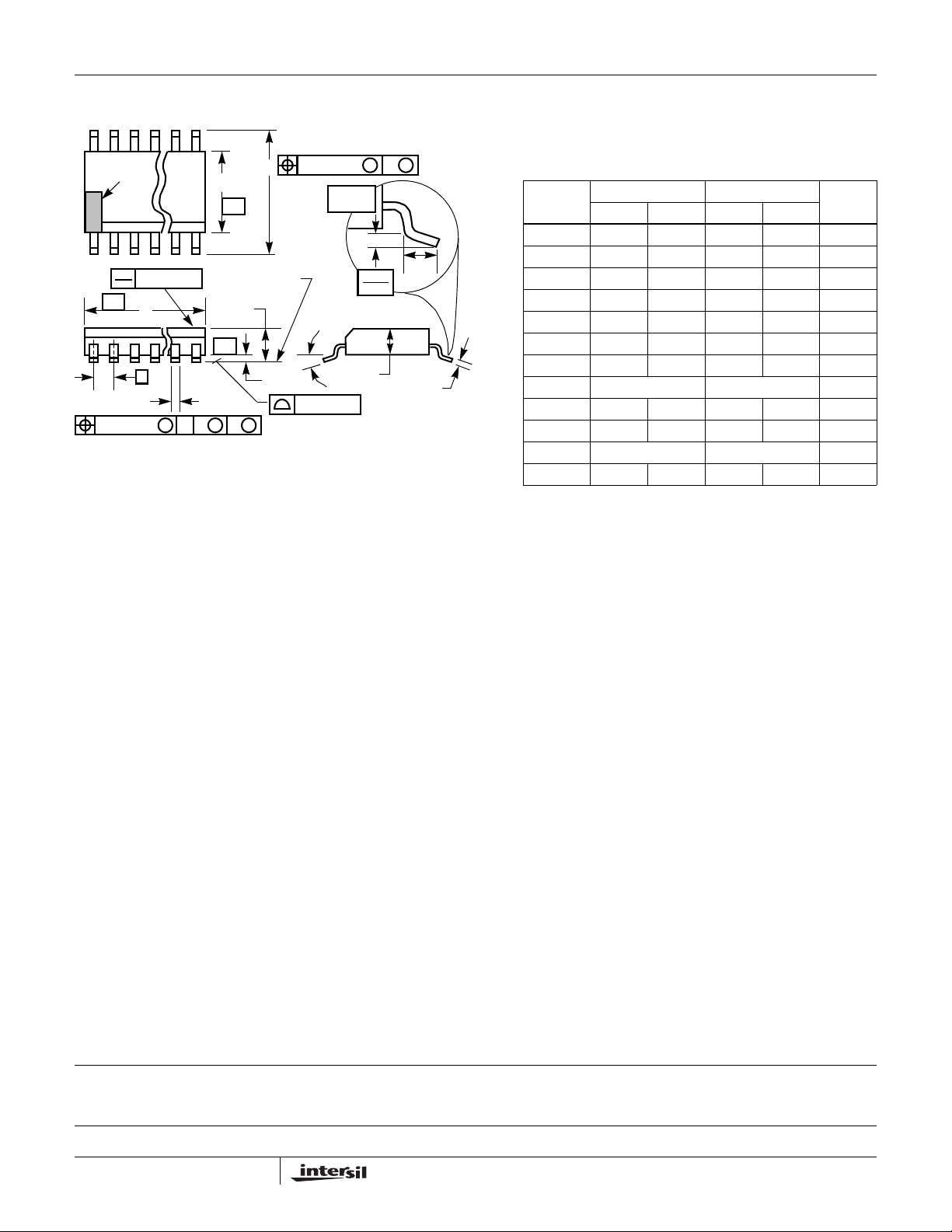
hin Shrink Small Outline Plastic Packages (TSSOP)
N
INDEX
AREA
123
-A-
0.05(0.002)
D
SEATING PLANE
e
b
0.10(0.004) C AM BS
M
E1
-B-
A
-C-
0.25(0.010) BM M
E
α
A1
0.10(0.004)
GAUGE
PLANE
0.25
0.010
A2
L
c
NOTES:
1. These package dimensions are within allowable dimensions of
JEDEC MO-153-AC, Issue E.
2. Dimensioning and tolerancing per ANSI Y14.5M-1982.
3. Dimension “D” does not include mold flash, protrusions or gate burrs.
Mold flash, protrusion and gate burrs shall not exceed 0.15mm
(0.006 inch) per side.
4. Dimension “E1” does not include interlead flash or protrusions. Interlead flash and protrusions shall not exceed 0.15mm (0.006 inch) per
side.
5. The chamfer on the body is optional. If it is not present, a visual index
feature must be located within the crosshatched area.
6. “L” is the length of terminal for soldering to a substrate.
7. “N” is the number of terminal positions.
8. Terminal numbers are shown for reference only.
9. Dimension “b” does not include dambar protrusion. Allowable dambar
protrusion shall be 0.08mm (0.003 inch) total in excess of “b” dimension at maximum material condition. Minimum space between protrusion and adjacent lead is 0.07mm (0.0027 inch).
10. Controlling dimension: MILLIMETER. Converted inch dimensions
are not necessarily exact. (Angles in degrees)
M14.173
14 LEAD THIN SHRINK SMALL OUTLINE PLASTIC
PACKAGE
INCHES MILLIMETERS
SYMBOL
A - 0.047 - 1.20 -
A1 0.002 0.006 0.05 0.15 -
A2 0.031 0.041 0.80 1.05 -
b 0.0075 0.0118 0.19 0.30 9
c 0.0035 0.0079 0.09 0.20 -
D 0.195 0.199 4.95 5.05 3
E1 0.169 0.177 4.30 4.50 4
e 0.026 BSC 0.65 BSC -
E 0.246 0.256 6.25 6.50 -
L 0.0177 0.0295 0.45 0.75 6
N14 147
o
α
0
o
8
o
0
o
8
NOTESMIN MAX MIN MAX
-
Rev. 2 4/06
All Intersil U.S. products are manufactured, assembled and tested utilizing ISO9000 quality systems.
Intersil Corporation’s quality certifications can be viewed at www.intersil.com/design/quality
Intersil products are sold by description only. Intersil Corporation reserves the right to make changes in circuit design, software and/or specifications at any time without
notice. Accordingly, the reader is cautioned to verify that data sheets are current before placing orders. Information furnished by Intersil is believed to be accurate and
reliable. However, no responsibility is assumed by Intersil or its subsidiaries for its use; nor for any infringements of patents or other rights of third parties which may result
from its use. No license is granted by implicat ion or oth erwise u nde r any p a tent or p at ent r ights of Intersil or its subsidiaries.
For information regarding Intersil Corporation and its products, see www.intersil.com
13
FN6180.0
July 17, 2006
 Loading...