

Page 1
查询ISL12028IBAZ供应商
®
ISL12029
New Features
Data Sheet FN6206.1
Real Time Clock/Calendar with EEPROM
The ISL12029 device is a low power real time clock with
clock/calender, power-fail indicator, clock output and crystal
compensation, two periodic or polled alarms (open drain
output), intelligent battery backup switching, CPU
Supervisor, integrated 512 x 8 bit EEPROM configured in 16
byte per page.
The oscillator uses an external, low-cost 32.768kHz crystal.
The real time clock tracks time with separate registers for
hours, minutes, and seconds. The device has calendar
registers for date, month, year and day of the week. The
calendar is accurate through 2099, with automatic leap year
correction.
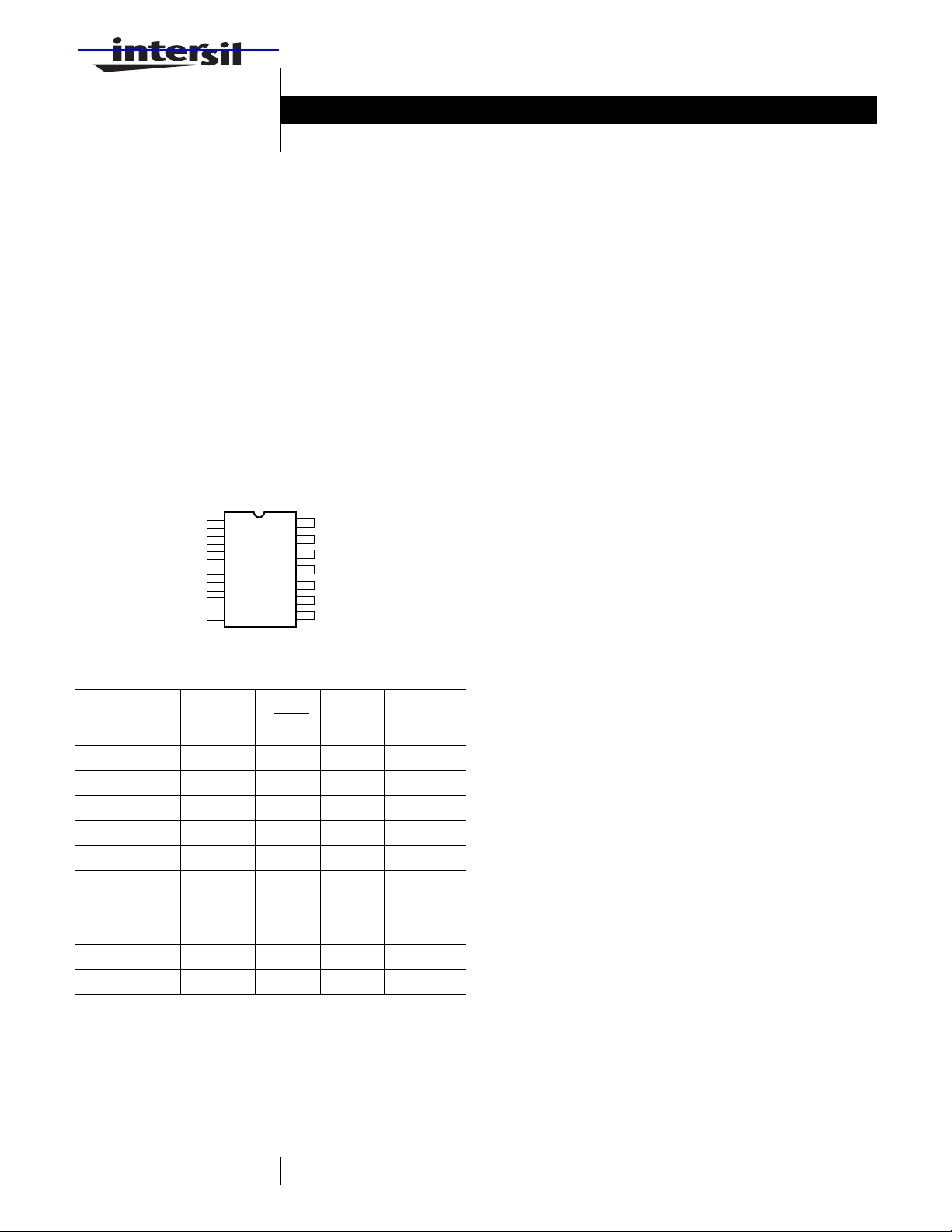
Pinout
14 LD TSSOP/SOIC
TOP VIEW
1
X1
2
X2
NC
NC
NC
RESET
GND
3
4
5
6
7
NC = No internal connection
V
14
13
12
11
10
DD
V
BAT
F
/IRQ
OUT
NC
NC
9
SCL
8
SDA
Ordering Information
TEMP.
PAR T N U MBER
(Note)
ISL12029IB27Z 12029IB27Z 2.63V -40 to +85 14 Ld SOIC
ISL12029IB27AZ* 2.92V -40 to +85 14 Ld SOIC
ISL12029IB30AZ* 3.09V -40 to +85 14 Ld SOIC
ISL12029IBZ 12029IBZ 4.38V -40 to +85 14 Ld SOIC
ISL12029IBAZ* 4.64V -40 to +85 14 Ld SOIC
ISL12029IV27Z 12029IV27Z 2.63V -40 to +85 14 Ld TSSOP
ISL12029IV27AZ* 2.92V -40 to +85 14 Ld TSSOP
ISL12029IV30AZ* 3.09V -40 to +85 14 Ld TSSOP
ISL12029IVZ 12029IVZ 4.38V -40 to +85 14 Ld TSSOP
ISL12029IVAZ* 4.64V -40 to +85 14 Ld TSSOP
NOTE: Intersil Pb-free plus anneal products employ special Pb-free
material sets; molding compounds/die attach materials and 100% matte tin
plate termination finish, which are RoHS compliant and compatible with
both SnPb and Pb-free soldering operations. Intersil Pb-free products are
MSL classified at Pb-free peak reflow temperatures that meet or exceed the
Pb-free requirements of IPC/JEDEC J STD-020.
Add “-T” suffix for Tape & Reel after the part number.
* Contact Factory for availability
PART
MARKING
V
RESET
VOLTAGE
RANGE
(°C)
PACKAGE
(Pb-free)
February 9, 2006
Features
• Real Time Clock/Calendar
- Tracks Time in Hours, Minutes, and Seconds
- Day of the Week, Day, Month, and Year
- 3 Selectable Frequency Outputs
• Two Non-Volatile Alarms
- Settable on the Second, Minute, Hour, Day of the Week,
Day, or Month
- Repeat Mode (periodic interrupts)
• Automatic Backup to Battery or SuperCap
- Power Failure Detection
- 800nA Battery Supply Current
• On-Chip Oscillator Compensation:
- Internal Feedback Resistor and Compensation
Capacitors
- 64 Position Digitally Controlled Trim Capacitor
- 6 Digital Frequency Adjustment Settings to ±30ppm
• 512 x 8 Bits of EEPROM
- 16-Byte Page Write Mode (32 total pages)
- 8 Modes of Block Lock™ Protection
- Single Byte Write Capability
- Data Retention: 50 years
- Endurance: 500,000 Cycles Per Byte
• CPU Supervisor Functions
- Power-On Reset, Low Voltage Sense
- Watchdog Timer (0.25s, 0.75s, 1.5s)
2
C* Interface - 400kHz Data Transfer Rate
•I
• 14 Ld SOIC and TSSOP Packages
• Pb-Free Plus Anneal Available (RoHS Compliant)
Applications
• Utility Meters
• HVAC Equipment
• Audio/Video Components
• Modems
• Network Routers, Hubs, Switches, Bridges
• Cellular Infrastructure Equipment
• Fixed Broadband Wireless Equipment
• Pagers/PDA
• POS Equipment
• Test Meters/Fixtures
• Office Automation (Copiers, Fax)
• Home Appliances
• Computer Products
• Other Industrial/Medical/AutomotivePAR
1
CAUTION: These devices are sensitive to electrostatic discharge; follow proper IC Handling Procedures.
1-888-INTERSIL or 1-888-468-3774
2
*I
C is a Trademark of Philips. Copyright Intersil Americas Inc. 2005-2006. All Rights Reserved
| Intersil (and design) is a registered trademark of Intersil Americas Inc.
All other trademarks mentioned are the property of their respective owners.
Page 2
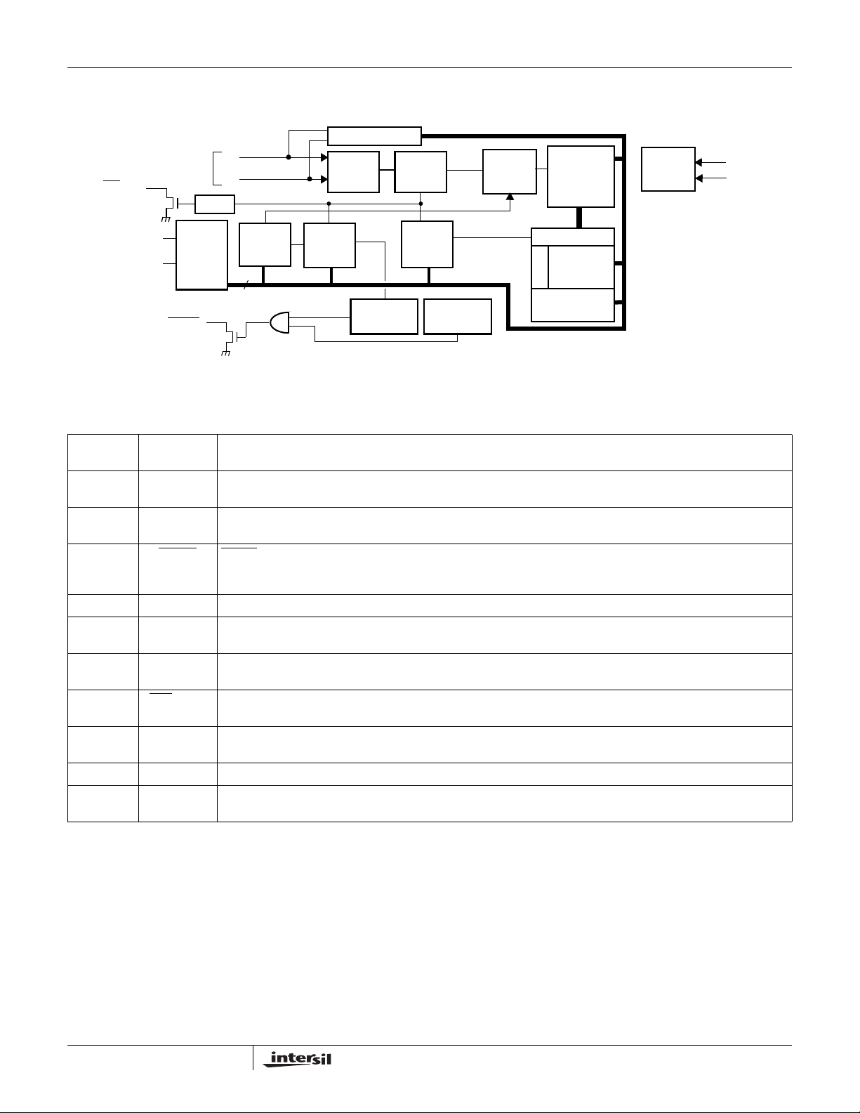
Block Diagram
32.768kHz
IRQ/F
OUT
Select
ISL12029
OSC Compensation
X1
X2
Oscillator
Frequency
Divider
1Hz
Timer
Calendar
Logic
Time
Keeping
Registers
(SRAM)
Battery
Switch
Circuitry
V
V
DD
BACK
Timer
Status
Registers
(SRAM)
Low Voltage
Reset
Alarm
Compare
Alarm Regs
Mask
EEPROM
(EEPROM)
4K
ARRAY
SCL
SDA
Interface
Decoder
RESET
Serial
Control
Decode
Logic
8
Control/
Registers
(EEPROM)
Watchdog
Pin Descriptions
PIN
NUMBER SYMBOL DESCRIPTION
1 X1 The X1 pin is the input of an inverting amplifier and is intended to be connected to one pin of an external 32.768kHz
quartz crystal.
2 X2 The X2 pin is the output of an inverting amplifier and is intended to be connected to one pin of an external 32.768kHz
quartz crystal.
6 RESET
7 GND Ground.
8 SDA Serial Data (SDA) is a bidirectional pin used to transfer serial data into and out of the device. It has an open drain
9 SCL The Serial Clock (SCL) input is used to clock all serial data into and out of the device. The input buffer on this pin is
12
13 V
14 V
3, 4, 5, 10,
IRQ/F
BAT
DD
N.C. No Internal Connection.
11
RESET. This is a reset signal output. This signal notifies a host processor that the “watchdog” time period has
expired or that the voltage has dropped below a fixed V
Recommended value for the pull-up resistor is 5kΩ, If unused, connect to ground.
threshold. It is an open drain active LOW output.
TRIP
output and may be wire OR’ed with other open drain or open collector outputs.
always active (not gated).
Interrupt Output/Frequency Output is a multi-functional pin that can be used as interrupt or frequency output pin. It
OUT
is an open drain output. The function is set via the configuration register.
This input provides a backup supply voltage to the device. V
V
supply fails. This pin should be tied to ground if not used.
DD
supplies power to the device in the event that the
BAT
Power Supply.
2
FN6206.1
February 9, 2006
Page 3
ISL12029
Absolute Maximum Ratings Thermal Information
Voltage on VDD, V
(respect to ground) . . . . . . . . . . . . . . . . . . . . . . . . . . -0.3V to 6.0V
, SCL, SDA, and IRQ/F
BAT
OUT
Pins
Voltage on X1 and X2 Pins
(respect to ground) . . . . . . . . . . . . . . . . . . . . . . . . . . -0.3V to 2.5V
ESD Rating
MIL-STD-883, Method 3014. . . . . . . . . . . . . . . . . . . . . . . . .>±2kV
Machine Model . . . . . . . . . . . . . . . . . . . . . . . . . . . . . . . . . . .>175V
CAUTION: Stresses above those listed in “Absolute Maximum Ratings” may cause permanent damage to the device. This is a stress only rating and operation of the
device at these or any other conditions above those indicated in the operational sections of this specification is not implied.
NOTE: θJA is measured with the component mounted on a high effective thermal conductivity test board in free air. See Tech Brief TB379 for details.
Thermal Resistance (Note) θ
(°C/W)
JA
14 Ld SOIC Package . . . . . . . . . . . . . . . . . . . . . . . . 100
14 Ld TSSOP Package . . . . . . . . . . . . . . . . . . . . . . 110
Storage Temperature . . . . . . . . . . . . . . . . . . . . . . . . -65°C to +150°C
Lead Temperature (Soldering, 10s) . . . . . . . . . . . . . . . . . . . . . 300°C
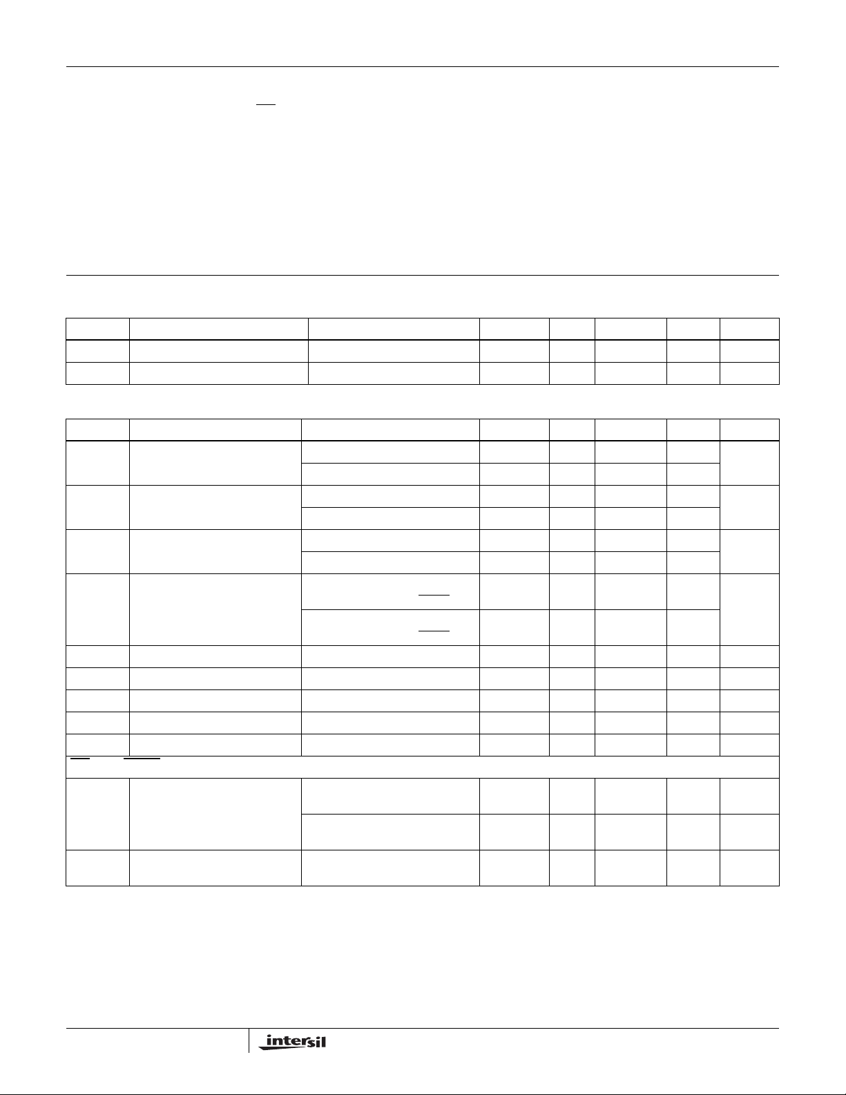
DC Electrical Specifications Unless otherwise noted, V
= 3.3V
V
DD
= +2.7V to +5.5V, TA= -40°C to +85°C, Typical values are at TA= 25°C and
DD
SYMBOL PARAMETER CONDITIONS MIN TYP MAX UNIT NOTES
V
V
BAT
Main Power Supply 2.7 5.5 V
DD
Backup Power Supply 1.8 5.5 V
Electrical Specifications
SYMBOL PARAMETER CONDITIONS MIN TYP MAX UNIT NOTES
I
DD1
I
DD2
I
DD3
I
BAT
I
BATLKG
V
TRIP
V
TRIPHYSVTRIP
V
BATHYSVBAT
V
DD SR-VDD
IRQ
/F
V
I
Supply Current with I2C Active VDD = 2.7V 500 µA 1, 2, 3
V
= 5.5V 800 µA
DD
Supply Current for Non-Volatile
Programming
Supply Current for Main
Timekeeping (Low Power Mode)
Battery Supply Current V
Battery Input Leakage VDD = 5.5V, V
V
Mode Threshold 1.8 2.2 2.6 V 5
BAT
VDD = 2.7V 2.5 mA 1, 2, 3
VDD = 5.5V 3.5 mA
VDD = V
VDD = V
BAT
V
DD
V
BAT
V
DD
SDA
SDA
= 1.8V,
= V
SDA
= 3.0V,
= V
SDA
= V
= 2.7V 10 µA 3
SCL
= V
= 5.5V 20 µA
SCL
800 1000 nA 1, 4, 5
= V
SCL
= V
RESET
= 0V
850 1200 nA
= V
= V
SCL
= 1.8V -100 100 nA
BAT
RESET
= 0V
Hysteresis 30 mV 5, 7
Hysteresis 50 mV 5, 7
Negative Slew Rate 10 V/ms 6
RESET OUTPUTS
OUT,
Output Low Voltage VDD = 5.5V
OL
Output Leakage Current VDD = 5.5V
LO
I
V
I
V
OL
DD
OL
OUT
= 3mA
= 2.7V
= 1mA
100 400 nA
=5.5V
0.4 V
0.4 V
, 3
3
FN6206.1
February 9, 2006
Page 4

ISL12029
Watchdog Timer/Low Voltage Reset Parameters
SYMBOL PARAMETER CONDITIONS MIN
t
RPD
t
PURST
V
RVALID
V
RESET
t
WDO
t
RST
t
RSP
EEPROM SPECIFICATIONS
VDD Detect to RESET LOW 500 ns 7
Power Up Reset Time-Out Delay 100 250 400 ms
Minimum VDD for Valid RESET
Output
ISL12029-4.5A Reset Voltage Level 4.59 4.64 4.69 V
ISL12029 Reset Voltage Level 4.33 4.38 4.43 V
ISL12029-3 Reset Voltage Level 3.04 3.09 3.14 V
ISL12029-2.7A Reset Voltage Level 2.87 2.92 2.97 V
ISL12029-2.7 Reset Voltage Level 2.58 2.63 2.68 V
Watchdog Timer Period 32.768kHz crystal between X1
and X2
Watchdog Timer Reset Time-Out
Delay
32.768kHz crystal between X1
and X2
I2C Interface Minimum Restart Time 1.2 µs
EEPROM Endurance 500,000 Cycles
EEPROM Retention Temperature ≤75°C 50 Years
TYP
(Note 5) MAX UNI TS NOTES
1.0 V
1.70 1.75 1.801 s
725 750 775 ms
225 250 275 ms
225 250 275 ms
Serial Interface (I2C) Specifications
DC/AC Characteristics
SYMBOL PARAMETER CONDITIONS MIN TYP MAX UNITS NOTES
V
V
SDA, and SCL Input Buffer LOW
IL
Voltage
SDA, and SCL Input Buffer HIGH
IH
Voltage
Hysteresis SDA and SCL Input Buffer
Hysteresis
V
I
I
SDA Output Buffer LOW Voltage IOL=4mA 0 0.4 V
OL
Input Leakage Current on SCL VIN= 5.5V 0.1 10 µA
LI
I/O Leakage Current on SDA VIN= 5.5V 0.1 10 µA
LO
TIMING CHARACTERISTICS
f
SCL
t
t
t
BUF
t
LOW
SCL Frequency 400 kHz
Pulse Width Suppression Time at
IN
SDA and SCL Inputs
SCL Falling Edge to SDA Output
AA
Data Valid
Time the Bus Must be Free Before
the Start of a New Transmission
Clock LOW Time Measured at the 30% of VDD
SBIB = 1 (Under VDD mode) -0.3 0.3 x V
SBIB = 1 (Under VDD mode) 0.7 x V
SBIB = 1 (Under V
mode) 0.05 x V
DD
Any pulse narrower than the max
DD
DD
VDD + 0.3 V
50 ns
spec is suppressed.
SCL falling edge crossing 30% of
V
, until SDA exits the 30% to
DD
70% of V
window.
DD
SDA crossing 70% of VDD during
1300 ns
900 ns
a STOP condition, to SDA
crossing 70% of V
following START condition.
during the
DD
1300 ns
crossing.
DD
V
V
4
FN6206.1
February 9, 2006
Page 5

ISL12029
Serial Interface (I2C) Specifications (Continued)
DC/AC Characteristics
SYMBOL PARAMETER CONDITIONS MIN TYP MAX UNITS NOTES
t
HIGH
t
SU:STA
t
HD:STA
t
SU:DAT
t
HD:DAT
t
SU:STO
t
HD:STO
t
DH
t
Clock HIGH Time Measured at the 70% of VDD
crossing.
START Condition Setup Time SCL rising edge to SDA falling
edge. Both crossing 70% of V
START Condition Hold Time From SDA falling edge crossing
30% of V
to SCL falling edge
DD
crossing 70% of V
Input Data Setup Time From SDA exiting the 30% to
70% of V
edge crossing 30% of V
window, to SCL rising
DD
Input Data Hold Time From SCL falling edge crossing
70% of V
30% to 70% of V
to SDA entering the
DD
STOP Condition Setup Time From SCL rising edge crossing
70% of V
, to SDA rising edge
DD
crossing 30% of V
STOP Condition Hold Time for
Read, or Volatile Only Write
From SDA rising edge to SCL
falling edge. Both crossing 70%
of V
.
DD
Output Data Hold Time From SCL falling edge crossing
30% of V
30% to 70% of V
SDA and SCL Rise Time From 30% to 70% of V
R
SDA and SCL Fall Time From 70% to 30% of V
t
F
, until SDA enters the
DD
DD
window.
DD
DD
window.
DD
DD
.
DD
.
DD
DD
Cb Capacitive Loading of SDA or SCL Total on-chip and off-chip 10 400 pF
Cpin SDA, and SCL Pin Capacitance 10 pF
t
WC
Non-Volatile Write Cycle Time 12 20 ms 8
600 ns
600 ns
.
600 ns
100 ns
0ns
600 ns
600 ns
0ns
20 +
250 ns
0.1 x Cb
20 +
250 ns
0.1 x Cb
NOTES:
F
1. IRQ/
2. V
3. V
Inactive (no frequency output and no alarms).
OUT
= VDD x 0.1, V
IL
= 2.63V (VDD must be greater than V
RESET
= VDD x 0.9, f
IH
SCL
= 400kHz.
RESET
), VBAT = 0V.
4. Bit BSW = 0 (Standard Mode), VBAT ≥ 1.8V.
5. Specified at 25°C.
6. In order to ensure proper timekeeping, the V
specification must be followed.
DD SR-
7. Parameter is not 100% tested.
is the minimum cycle time to be allowed for any non-volitile Write by the user, it is the time from valid STOP condition at the end of Write
8. t
WC
sequence of a serial interface Write operation, to the end of the self-timed internal non-volatile write cycle.
5
FN6206.1
February 9, 2006
Page 6
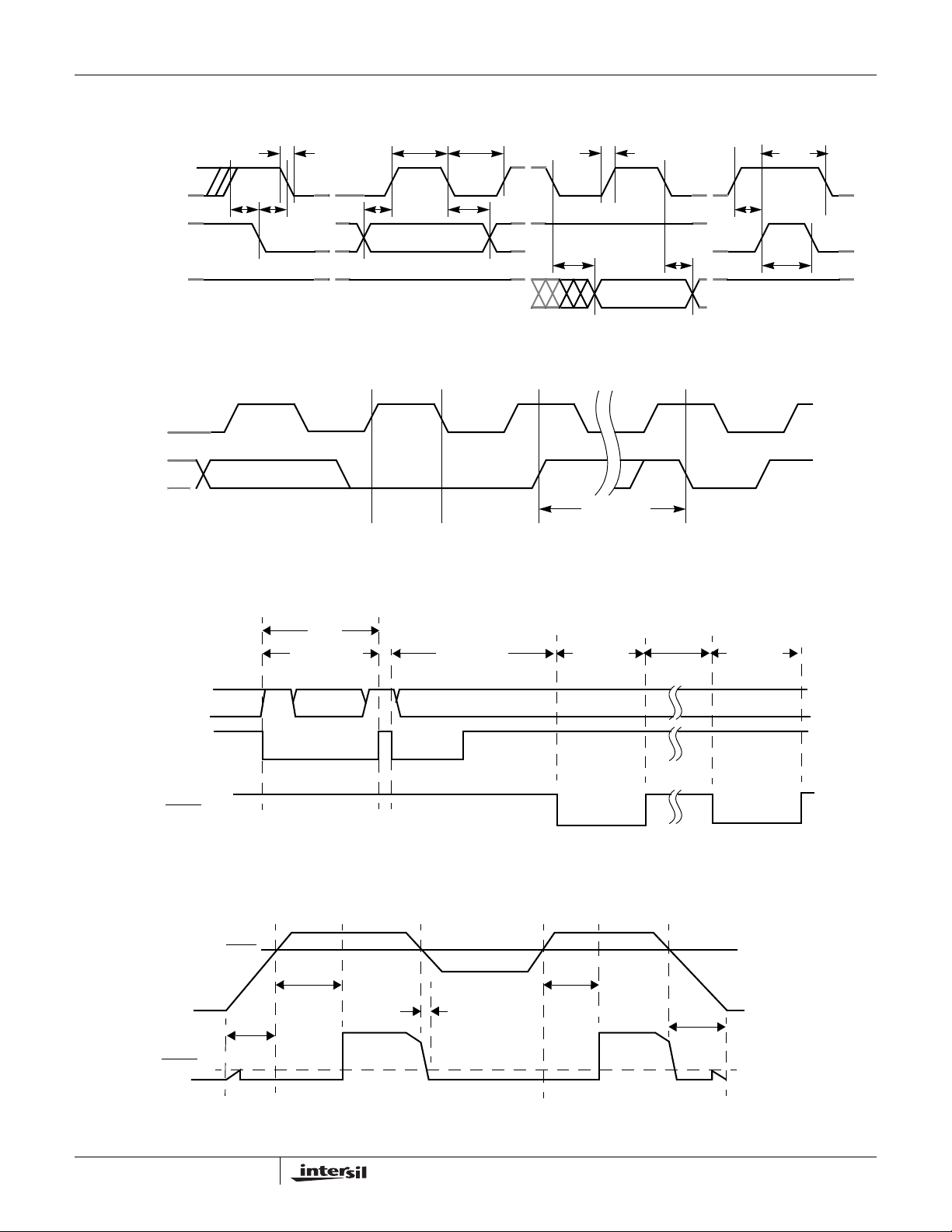
Timing Diagrams
ISL12029
SCL
SDA
(INPUT TIMING)
SDA
(OUTPUT TIMING)
SCL
SDA
t
F
t
SU:DAT
t
SU:STA
t
HD:STA
8TH BIT OF LAST BYTE ACK
t
HIGH
t
LOW
t
HD:DAT
FIGURE 1. BUS TIMING
STOP
CONDITION
FIGURE 2. WRITE CYCLE TIMING
t
R
t
DH
t
AA
t
WC
START
CONDITION
t
BUF
t
HD:STO
t
SU:STO
SCL
SDA
RESET
V
RESET
DD
V
RESET
t
RSP
t
RSP>tWDO
START
t
RSP<tWDO
STOP
START
Note: All inputs are ignored during the active reset period (t
FIGURE 3. WATCHDOG TIMING
t
PURST
t
R
t
RPD
t
PURST
t
RST
RST
t
RSP>tWDO
t
RST
).
t
F
V
RVALID
FIGURE 4. RESET TIMING
6
FN6206.1
February 9, 2006
Page 7
ISL12029
Typical Performance Curves Temperature is 25°C unless otherwise specified
0.90
4.00
3.50
3.00
2.50
2.00
Ibat (uA)
1.50
1.00
0.50
0.00
1.8 2.3 2.8 3.3 3.8 4.3 4.8 5.3
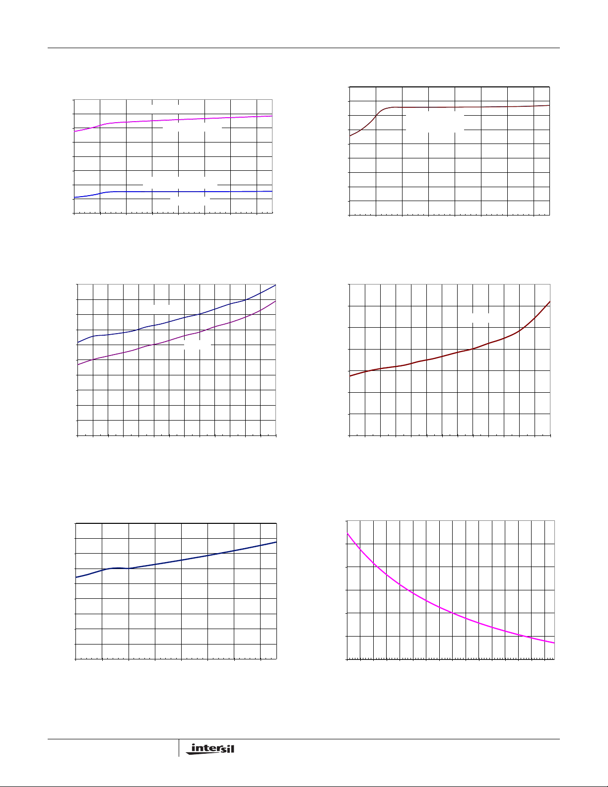
FIGURE 5. I
BSW = 0 or 1
SCL,SDA pullups = 0 V
SCL,SDA pul lups = Vbat
BSW = 0 or 1
Vbat (V)
BAT
vs V
SBIB = 0 FIGURE 6. I
BAT,
0.80
0.70
0.60
0.50
Ibat
0.40
0.30
0.20
0.10
0.00
1.80 2.30 2.80 3.30 3.80 4.30 4.80 5.30
SCL,SDA pullups = 0V
BSW = 0 or 1
Vbat(V)
vs V
BAT
BAT,
SBIB = 1
5.00
4.50
4.00
3.50
3.00
2.50
Idd (uA)
2.00
1.50
1.00
0.50
0.00
-45-35-25-15-5 5 1525354555657585
Vdd=5.5V
Vdd=3.3V
Temperature
FIGURE 7. I
4.50
4.00
3.50
3.00
2.50
2.00
Idd (uA)
1.50
1.00
0.50
0.00
1.8 2.3 2.8 3.3 3.8 4.3 4.8 5.3
vs TEMPERATURE FIGURE 8. I
DD3
Vdd (V)
1.40
1.20
Vbat = 3.0V
1.00
0.80
0.60
Ibat (uA)
0.40
0.20
0.00
-45-35-25-15-5 5 1525354555657585
Temperature
vs TEMPERATURE
BAT
80
60
40
20
0
PPM change from ATR=0
-20
-40
-32 -28 -24 -20 -16 -12 -8 -4 0 4 8 12 16 20 24 28
ATR set ti ng
FIGURE 9. I
DD3
7
vs V
DD
FIGURE 10. ∆F
vs ATR SETTING
OUT
FN6206.1
February 9, 2006
Page 8

ISL12029
Description
The ISL12029 device is a Real Time Clock with clock/calendar,
two polled alarms with integrated 512x8 EEPROM, oscillator
compensation, CPU Supervisor (Power-on Reset, Low Voltage
Sensing and Watchdog Timer) and battery backup switch.
The oscillator uses an external, low-cost 32.768kHz crystal.
All compensation and trim components are integrated on the
chip. This eliminates several external discrete components
and a trim capacitor, saving board area and component cost.
The Real-Time Clock keeps track of time with separate
registers for Hours, Minutes, Seconds. The Calendar has
separate registers for Date, Month, Year and Day-of-week.
The calendar is correct through 2099, with automatic leap
year correction.
The Dual Alarms can be set to any Clock/Calendar value for a
match. For instance, every minute, every Tuesday, or 5:23 AM
on March 21. The alarms can be polled in the Status Register
or can provide a hardware interrupt (IRQ
/F
Pin). There is a
OUT
repeat mode for the alarms allowing a periodic interrupt.
The IRQ
/F
pin may be software selected to provide a
OUT
frequency output of 1Hz, 4096Hz, or 32,768Hz or inactive.
The ISL12029 device integrates CPU Supervisory functions
(POR, WDT) and Battery Switch. There is Power-On-Reset
(RESET
VDD supply crosses the V
also assert RESET
V
) output with 250ms delay from power-on when the
threshold for the device. It will
RESET
when V
threshold for the device. The V
RESET
goes below the specified
DD
RESET
threshold is
selectable via VTS2/VTS1/VTS0 registers to five (5)
preselected levels. Their is WatchDog Timer (WDT) with 3
selectable time-out periods (0.25s, 0.75s and 1.75s) and
disabled setting. The WatchDog Timer activates the RESET
when it expires. Normally, the I
RESET
output is active, but this can be changed by using a
register bit to enable I
2
The device offers a backup power input pin. This V
2
C Interface is disabled when the
C operation in battery backup mode.
BAT
pin
pin
allows the device to be backed up by battery or SuperCap. The
entire ISL12029 device is fully operational from 2.7 to 5.5V and
the clock/calendar portion of the ISL12029 device remains fully
operational down to 1.8V (Standby Mode).
The ISL12029 device provides 4K bits of EEPROM with 8
modes of BlockLock™ control. The BlockLock allows a safe,
secure memory for critical user and configuration data, while
allowing a large user storage area.
Pin Descriptions
Serial Clock (SCL)
The SCL input is used to clock all data into and out of the
device. The input buffer on this pin is always active (not
gated). The pull-up resistor on this pin must use the same
voltage source as V
DD
.
Serial Data (SDA)
SDA is a bidirectional pin used to transfer data into and out
of the device. It has an open drain output and may be wire
ORed with other open drain or open collector outputs. The
input buffer is always active (not gated).
This open drain output requires the use of a pull-up resistor.
The pull-up resistor on this pin must use the same voltage
source as V
. The output circuitry controls the fall time of the
DD
output signal with the use of a slope controlled pull-down. The
circuit is designed for 400kHz I
V
BAT
2
C interface speed.
This input provides a backup supply voltage to the device.
V
supplies power to the device in the event the VDD
BAT
supply fails. This pin can be connected to a battery, a
SuperCap or tied to ground if not used.
IRQ/F
(Interrupt Output/Frequency Output)
OUT
This dual function pin can be used as an interrupt or
frequency output pin. The IRQ
/F
mode is selected via
OUT
the frequency out control bits of the control/status register.
• Interrupt Mode. The pin provides an interrupt signal
output. This signal notifies a host processor that an alarm
has occurred and requests action. It is an open drain
active low output.
• Frequency Output Mode. The pin outputs a clock signal
which is related to the crystal frequency. The frequency
output is user selectable and enabled via the I
2
C bus. It is
an open drain output.
The IRQ
/F
pin is an open drain output requiring a pullup
OUT
resistor which was intended to be used for clocking
applications for microcontrollers. Choose the pullup resistor
with care, since low values will cause high currents to flow in
the V
and ground traces around the device which can
DD
contribute to faulty oscillator function. For a 32kHz output,
values up to 10kΩ can be used with some degradation of the
square waveform.
RESET
The RESET signal output can be used to notify a host
processor that the watchdog timer has expired or the VDD
voltage supply has dipped below the V
threshold. It is
RESET
an open drain, active LOW output. Recommended value for
the pullup resistor is 10kΩ. If unused it can be tied to ground.
X1, X2
The X1 and X2 pins are the input and output, respectively, of
an inverting amplifier. An external 32.768kHz quartz crystal is
used with the ISL12029 to supply a timebase for the real time
clock. Internal compensation circuitry provides high accuracy
over the operating temperature range from -40°C to +85°C.
This oscillator compensation network can be used to calibrate
the crystal timing accuracy over temperature either during
manufacturing or with an external temperature sensor and
microcontroller for active compensation. X2 is intended to
drive a crystal only, and should not drive any external circuit.
8
FN6206.1
February 9, 2006
Page 9

ISL12029
NO EXTERNAL COMPENSATION RESISTORS OR
CAPACITORS ARE NEEDED OR ARE RECOMMENDED
TO BE CONNECTED TO THE X1 AND X2 PINS.
X1
X2
FIGURE 11. RECOMMENDED CRYSTAL CONNECTION
Real Time Clock Operation
The Real Time Clock (RTC) uses an external 32.768kHz
quartz crystal to maintain an accurate internal representation
of the second, minute, hour, day, date, month, and year. The
RTC has leap-year correction. The clock also corrects for
months having fewer than 31 days and has a bit that controls
24 hour or AM/PM format. When the ISL12029 powers up
after the loss of both V
operate until at least one byte is written to the clock register.
Reading the Real Time Clock
The RTC is read by initiating a Read command and
specifying the address corresponding to the register of the
Real Time Clock. The RTC Registers can then be read in a
Sequential Read Mode. Since the clock runs continuously
and read takes a finite amount of time, there is a possibility
that the clock could change during the course of a read
operation. In this device, the time is latched by the read
command (falling edge of the clock on the ACK bit prior to
RTC data output) into a separate latch to avoid time changes
during the read operation. The clock continuoes to run.
Alarms occuring during a read are unaffected by the read
operation.
Writing to the Real Time Clock
The time and date may be set by writing to the RTC
registers. RTC Register should be written ONLY with Page
Write. To avoid changing the current time by an uncompleted
write operation, write to the all 8 bytes in one write
operation. When writing the RTC registers, the new time
value is loaded into a separate buffer at the falling edge of
the clock during the Acknowledge. This new RTC value is
loaded into the RTC Register by a stop bit at the end of a
valid write sequence. An invalid write operation aborts the
time update procedure and the contents of the buffer are
discarded. After a valid write operation the RTC will reflect
the newly loaded data beginning with the next “one second”
clock cycle after the stop bit is written. The RTC continues to
update the time while an RTC register write is in progress
and the RTC continues to run during any nonvolatile write
sequences.
DD
and V
, the clock will not
BAT
Accuracy of the Real Time Clock
The accuracy of the Real Time Clock depends on the
accuracy of the quartz crystal that is used as the time base
for the RTC. Since the resonant frequency of a crystal is
temperature dependent, the RTC performance will also be
dependent upon temperature. The frequency deviation of
the crystal is a function of the turnover temperature of the
crystal from the crystal’s nominal frequency. For example, a
>20ppm frequency deviation translates into an accuracy of
>1 minute per month. These parameters are available from
the crystal manufacturer. Intersil’s RTC family provides onchip crystal compensation networks to adjust loadcapacitance to tune oscillator frequency from -34ppm to
+80ppm when using a 12.5pF load crystal. For more detailed
information see the Application section.
Clock/Control Registers (CCR)
The Control/Clock Registers are located in an area separate
from the EEPROM array and are only accessible following a
slave byte of “1101111x” and reads or writes to addresses
[0000h:003Fh]. The clock/control memory map has memory
addresses from 0000h to 003Fh. The defined addresses are
described in Table 2. Writing to and reading from the
undefined addresses are not recommended.
CCR Access
The contents of the CCR can be modified by performing a
byte or a page write operation directly to any address in the
CCR. Prior to writing to the CCR (except the status register),
however, the WEL and RWEL bits must be set using a three
step process (See section “Writing to the Clock/Control
Registers.”)
The CCR is divided into 5 sections. These are:
1. Alarm 0 (8 bytes; non-volatile)
2. Alarm 1 (8 bytes; non-volatile)
3. Control (5 bytes; non-volatile)
4. Real Time Clock (8 bytes; volatile)
5. Status (1 byte; volatile)
Each register is read and written through buffers. The nonvolatile portion (or the counter portion of the RTC) is updated
only if RWEL is set and only after a valid write operation and
stop bit. A sequential read or page write operation provides
access to the contents of only one section of the CCR per
operation. Access to another section requires a new
operation. A read or write can begin at any address in the
CCR.
It is not necessary to set the RWEL bit prior to writing the
status register. Section 5 (status register) supports a single
byte read or write only. Continued reads or writes from this
section terminates the operation.
The state of the CCR can be read by performing a random
read at any address in the CCR at any time. This returns the
contents of that register location. Additional registers are
9
FN6206.1
February 9, 2006
Page 10

ISL12029
read by performing a sequential read. The read instruction
latches all Clock registers into a buffer, so an update of the
clock does not change the time being read. A sequential
read of the CCR will not result in the output of data from the
memory array. At the end of a read, the master supplies a
stop condition to end the operation and free the bus. After a
read of the CCR, the address remains at the previous
address +1 so the user can execute a current address read
of the CCR and continue reading the next Register.
Real Time Clock Registers (Volatile)
SC, MN, HR, DT, MO, YR: Clock/Calendar Registers
These registers depict BCD representations of the time. As
such, SC (Seconds) and MN (Minutes) range from 00 to 59,
HR (Hour) is 1 to 12 with an AM or PM indicator (H21 bit) or
0 to 23 (with MIL = 1), DT (Date) is 1 to 31, MO (Month) is 1
to 12, YR (Year) is 0 to 99.
DW: Date of the Week Register
This register provides a Day of the Week status and uses
three bits DY2 to DY0 to represent the seven days of the
week. The counter advances in the cycle 0-1-2-3-4-5-6-0-12-… The assignment of a numerical value to a specific day
of the week is arbitrary and may be decided by the system
software designer. The default value is defined as ‘0’.
Y2K: Year 2000 Register
Can have value 19 or 20. As of the date of the introduction of
this device, there would be no real use for the value 19 in a
true real time clock, however.
24 Hour Time
If the MIL bit of the HR register is 1, the RTC uses a 24-hour
format. If the MIL bit is 0, the RTC uses a 12-hour format and
H21 bit functions as an AM/PM indicator with a ‘1’,
representing PM. The clock defaults to standard time with
H21 = 0.
Leap Years
Leap years add the day February 29 and are defined as
those years that are divisible by 4.
Status Register (SR) (Volatile)
The Status Register is located in the CCR memory map at
address 003Fh. This is a volatile register only and is used to
control the WEL and RWEL write enable latches, read power
status and two alarm bits. This register is separate from both
the array and the Clock/Control Registers (CCR).
TABLE 1. STATUS REGISTER (SR)
ADDR 7 6 5 4 3 2 1 0
003Fh BAT AL1 AL0 OSCF 0 RWEL WEL RTCF
Default 0 0 0 0 0 0 0 1
BAT: Battery Supply
This bit set to “1” indicates that the device is operating from
V
, not VDD. It is a read-only bit and is set/reset by
BAT
hardware (ISL12029 internally). Once the device begins
operating from V
, the device sets this bit to “0”.
DD
AL1, AL0: Alarm Bits
These bits announce if either alarm 0 or alarm 1 match the
real time clock. If there is a match, the respective bit is set to
‘1’. The falling edge of the last data bit in a SR Read
operation resets the flags. Note: Only the AL bits that are set
when an SR read starts will be reset. An alarm bit that is set
by an alarm occurring during an SR read operation will
remain set after the read operation is complete.
OSCF: Oscillator Fail Indicator
This bit is set to “1” if the oscillator is not operating. The bit is
set to “0” only if the oscillator is functioning. This bit is read
only, and is set /reset by hardware.
RWEL: Register Write Enable Latch
This bit is a volatile latch that powers up in the LOW
(disabled) state. The RWEL bit must be set to “1” prior to any
writes to the Clock/Control Registers. Writes to RWEL bit do
not cause a nonvolatile write cycle, so the device is ready for
the next operation immediately after the stop condition. A
write to the CCR requires both the RWEL and WEL bits to be
set in a specific sequence.
WEL: Write Enable Latch
The WEL bit controls the access to the CCR during a write
operation. This bit is a volatile latch that powers up in the
LOW (disabled) state. While the WEL bit is LOW, writes to
the CCR address will be ignored, although acknowledgment
is still issued. The WEL bit is set by writing a “1” to the WEL
bit and zeroes to the other bits of the Status Register. Once
set, WEL remains set until either reset to 0 (by writing a “0”
to the WEL bit and zeroes to the other bits of the Status
Register) or until the part powers up again. Writes to WEL bit
do not cause a nonvolatile write cycle, so the device is ready
for the next operation immediately after the stop condition.
RTCF: Real Time Clock Fail Bit
This bit is set to a ‘1’ after a total power failure. This is a
read only bit that is set internally when the device powers
up after having lost all power to the device (both V
V
= 0V). The bit is set regardless of whether VDD or
BAT
V
is applied first. The loss of only one of the supplies
BAT
does not result in setting the RTCF bit. The first valid write
to the RTC after a complete power failure (writing one byte
is sufficient) resets the RTCF bit to ‘0’.
DD
and
Unused Bits:
Bit 3 in the SR is not used, but must be zero. The Data Byte
output during a SR read will contain a zero in this bit
location.
10
FN6206.1
February 9, 2006
Page 11
ISL12029
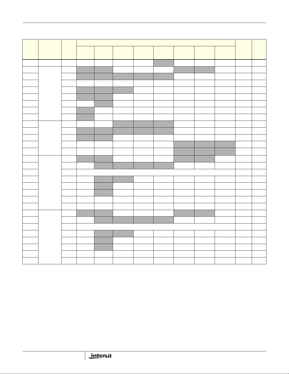
TABLE 2. CLOCK/CONTROL MEMORY MAP (Shaded cells indicate that NO other value is to be written to that bit. X indicates the bits are set
according to the product variation, see device ordering information)
BIT
REG
ADDR. TYPE
003F Status SR BAT AL1 AL0 OSCF
0037 RTC
0036 DW
0035 YR Y23 Y22 Y21 Y20 Y13 Y12 Y11 Y10 0-99 00h
0034 MO
0033 DT
0032 HR MIL
0031 MN
0030 SC
0014 Control
0013 DTR
0012 ATR
0011 INT IM AL1E AL0E FO1 FO0
0010 BL BP2 BP1 BP0 WD1 WD0
000F Alarm1
000E DWA1 EDW1
000D YRA1 Unused - Default = RTC Year value (No EEPROM) - Future expansion
000C MOA1 EMO1
000B DTA1 EDT1
000A HRA1 EHR1
0009 MNA1 EMN1 A1M22 A1M21 A1M20 A1M13 A1M12 A1M11 A1M10 0-59 00h
0008 SCA1 ESC1 A1S22 A1S21 A1S20 A1S13 A1S12 A1S11 A1S10 0-59 00h
0007 Alarm0
0006 DWA0 EDW0
0005 YRA0 Unused - Default = RTC Year value (No EEPROM) - Future expansion
0004 MOA0 EMO0
0003 DTA0 EDT0
0002 HRA0 EHR0
0001 MNA0 EMN0 A0M22 A0M21 A0M20 A0M13 A0M12 A0M11 A0M10 0-59 00h
0000 SCA0 ESC0 A0S22 A0S21 A0S20 A0S13 A0S12 A0S11 A0S10 0-59 00h
(SRAM)
(EEPROM)
(EEPROM)
(EEPROM)
NAME
Y2K
PWR SBIB BSW
Y2K1
Y2K0
7 6 5 4 3 2 1 0
0 0 Y2K21 Y2K20 Y2K13 0 0 Y2K10 19/20 20h
0 0 0 0 0 DY2 DY1 DY0 0-6 00h
0 0 0 G20 G13 G12 G11 G10 1-12 01h
0 0 D21 D20 D13 D12 D11 D10 1-31 00h
0 M22 M21 M20 M13 M12 M11 M10 0-59 00h
0 S22 S21 S20 S13 S12 S11 S10 0-59 00h
0 0 0 0 0 DTR2DTR1DTR0 00h
0 0 ATR5 ATR4 ATR3 ATR2 ATR1 ATR0 00h
0 0 A1Y2K21 A1Y2K20 A1Y2K13 0 0 A1Y2K10 19/20 20h
0 0 A0Y2K21 A0Y2K20 A0Y2K13 0 0 A0Y2K10 19/20 20h
RANGE
0 RWEL WEL RTCF 01h
0 H21 H20 H13 H12 H11 H10 0-23 00h
0 0 0 VTS2VTS1VTS0 4Xh
0 0 0 00h
0 0 0 18h
0 0 0 0 DY2 DY1 DY0 0-6 00h
0 0 A1G20 A1G13 A1G12 A1G11 A1G10 1-12 00h
0 A1D21 A1D20 A1D13 A1D12 A1D11 A1D10 1-31 00h
0 A1H21 A1H20 A1H13 A1H12 A1H11 A1H10 0-23 00h
0 0 0 0 DY2 DY1 DY0 0-6 00h
0 0 A0G20 A0G13 A0G12 A0G11 A0G10 1-12 00h
0 A0D21 A0D20 A0D13 A0D12 A0D11 A0D10 1-31 00h
0 A0H21 A0H20 A0H13 A0H12 A0H11 A0H10 0-23 00h
DEFAULT
Alarm Registers (Non-Volatile)
Addresses 0Ch to 0Fh
The alarm register bytes are set up identical to the RTC
register bytes, except that the MSB of each byte functions as
an enable bit (enable = “1”). These enable bits specify which
alarm registers (seconds, minutes, etc.) are used to make
the comparison. Note that there is no alarm byte for year.
The alarm function works as a comparison between the
alarm registers and the RTC registers. As the RTC
advances, the alarm will be triggered once a match occurs
between the alarm registers and the RTC registers. Any one
alarm register, multiple registers, or all registers can be
11
enabled for a match. See the Device Operation and
Application section for more information.
Control Registers (Non-Volatile)
The Control Bits and Registers described under this section
are nonvolatile.
BL Register
BP2, BP1, BP0 - Block Protect Bits
The Block Protect Bits, BP2, BP1 and BP0, determine which
blocks of the array are write protected. A write to a protected
block of memory is ignored. The block protect bits will
FN6206.1
February 9, 2006
Page 12
ISL12029
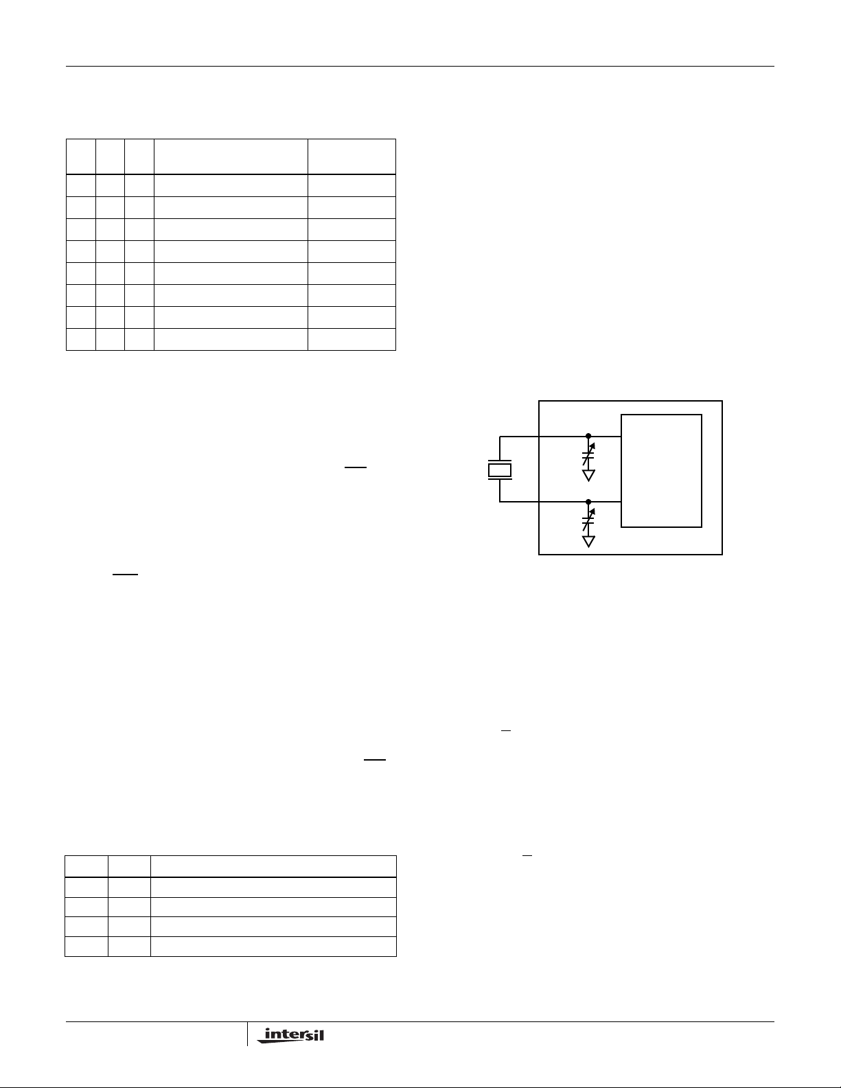
prevent write operations to one of eight segments of the
array. The partitions are described in Table 3.
TABLE 3.
PROTECTED ADDRESSES
BP2
BP1
BP0
0 0 0 None (Default) None
0 0 1 180
0 1 0 100
0 1 1 000
100 000h – 03F
101 000
1 1 0 000
1 1 1 000
ISL12029 ARRAY LOCK
– 1FF
h
– 1FF
h
– 1FF
h
– 07F
h
– 0FF
h
– 1FF
h
h
h
h
h
h
h
h
Upper 1/4
Upper 1/2
Full Array
First 4 Pages
First 8 Pages
First 16 Pages
Full Array
INT Register: Interrupt Control and
Frequency Output Register
IM, AL1E, AL0E - Interrupt Control and Status Bits
There are two Interrupt Control bits, Alarm 1 Interrupt Enable
(AL1E) and Alarm 0 Interrupt Enable (AL0E) to specifically
enable or disable the alarm interrupt signal output (IRQ
F
). The interrupts are enabled when either the AL1E or
OUT
AL0E or both bits are set to ‘1’ and both the FO1 and FO0
bits are set to 0 (Fout disabled).
/
Oscillator Compensation Registers
There are two trimming options.
- ATR. Analog Trimming Register
- DTR. Digital Trimming Register
These registers are non-volatile. The combination of analog
and digital trimming can give up to -64 to +110 ppm of total
adjustment.
ATR Register - AT R 5, AT R 4, AT R3 , ATR2, ATR1,
ATR0: Analog Trimming Register
Six analog trimming bits, ATR0 to ATR5, are provided in
order to adjust the on-chip load capacitance value for
frequency compensation of the RTC. Each bit has a different
weight for capacitance adjustment. For example, using a
Citizen CFS-206 crystal with different ATR bit combinations
provides an estimated ppm adjustment range from -34 to
+80ppm to the nominal frequency compensation.
X1
C
X1
X2
C
X2
Crystal
Oscillator
The IM bit enables the pulsed interrupt mode. To enter this
mode, the AL0E or AL1E bits are set to “1”, and the IM bit to
“1”. The IRQ/
F
output will now be pulsed each time an
OUT
alarm occurs. This means that once the interrupt mode
alarm is set, it will continue to alarm for each occurring
match of the alarm and present time. This mode is
convenient for hourly or daily hardware interrupts in
microcontroller applications such as security cameras or
utility meter reading.
In the case both Alarms are enabled.
FO1, FO0 - Programmable Frequency Output Bits
These are two output control bits. They select one of three
divisions of the internal oscillator, that is applied to the IRQ
F
output pin. Table 4 shows the selection bits for this
OUT
output. When using this function, the Alarm output function is
disabled.
TABLE 4. PROGRAMMABLE FREQUENCY OUTPUT BITS
FO1 FO0 OUTPUT FREQUENCY
0 0 Alarm output (F
0 1 32.768kHz
1 0 4096Hz
11 1Hz
OUT
disabled)
FIGURE 12. DIAGRAM OF ATR
The effective on-chip series load capacitance, C
LOAD
,
ranges from 4.5pF to 20.25pF with a mid-scale value of
12.5pF (default). C
controlled capacitors, C
and X2 pins to ground (see Figure 11). The value of C
C
is given by the following formula:
X2
C
16 b5⋅ 8b4 4b3 2b2 1b1 0.5b0 9+⋅+⋅+⋅+⋅+⋅+()pF=
X
/
The effective series load capacitance is the combination of
is changed via two digitally
LOAD
and CX2, connected from the X1
X1
X1
and
CX1 and CX2:
C
LOAD
C
LOAD
For example, C
C
(ATR = 100000) = 4.5pF, and C
LOAD
1
=
---------------------------------- -
=
1
1
---------- -
---------- -+
C
C
X1
X2
⋅ 8 b4 4 b3 2 b2 1 b1 0.5 b0 9+⋅+⋅+⋅+⋅+⋅+
16 b5
----------------------------------------------------------- ----------------------------------------------------------- -------
(ATR = 00000) = 12.5pF,
LOAD
2
(ATR = 011111)
LOAD
pF
= 20.25pF. The entire range for the series combination of
load capacitance goes from 4.5pF to 20.25pF in 0.25pF
steps. Note that these are typical values.
12
FN6206.1
February 9, 2006
Page 13

ISL12029
DTR Register - DTR2, DTR1, DTR0: Digital
Trimming Register
The digital trimming Bits DTR2, DTR1 and DTR0 adjust the
number of counts per second and average the ppm error to
achieve better accuracy.
DTR2 is a sign bit. DTR2 = 0 means frequency
compensation is > 0. DTR2 = 1 means frequency
compensation is < 0.
DTR1 and DTR0 are scale bits. DTR1 gives 10ppm
adjustment and DTR0 gives 20ppm adjustment.
A range from -30ppm to +30ppm can be represented by
using three bits above.
TABLE 5. DIGITAL TRIMMING REGISTERS
DTR REGISTER
000 0
010 +10
001 +20
011 +30
100 0
110 -10
101 -20
111 -30
ESTIMATED FREQUENCY
PPMDTR2 DTR1 DTR0
PWR Register: SBIB, BSW, VTS2, VTS1, VTS0
SBIB: - Serial Bus Interface (Enable)
The serial bus can be disabled in battery backup mode by
setting this bit to “1”. This will minimize power drain on the
battery. The Serial Interface can be enabled in battery
backup mode by setting this bit to “0”. (default is “0”). See
Reset and Power Control section.
BSW: Power Control Bit
The Power Control bit, BSW, determines the conditions for
switching between V
options.
Option 1. Standard: Set “BSW = 0”
Option 2. Legacy/Default Mode: Set “BSW = 1”
See Power Control Operation later in this document for more
details. Also see “I
backup and LVR Operation” in the Applications section for
important details.
VTS2, VTS1, VTS0: V
The ISL12029 is shipped with a default VDD threshold
(V
a nonvolatile with no protection, therefore any writes to this
location can change the default value from that marked on
the package. If not changed with a nonvolatile write, this
) per the ordering information table. This register is
RESET
and Back Up Battery. There are two
DD
2
C Communications During Battery
Select Bits
RESET
value will not change over normal operating and storage
conditions. However, ISL12029 has four (4) additional
selectable levels to fit the customers application. Levels are:
4.64V(default), 4.38V, 3.09V, 2.92V and 2.63V. The V
RESET
selection is via 3 bits (VTS2, VTS1 and VTS0). See Table 6
below.
TABL E 6 .
VTS2 VTS1 VTS0 V
0 0 0 4.64V
0 0 1 4.38V
0 1 0 3.09V
0 1 1 2.92V
1 0 0 2.63V
RESET
Device Operation
Writing to the Clock/Control Registers
Changing any of the bits of the clock/control registers
requires the following steps:
1. Write a 02h to the Status Register to set the Write Enable
Latch (WEL). This is a volatile operation, so there is no
delay after the write. (Operation preceded by a start and
ended with a stop).
2. Write a 06h to the Status Register to set both the Register
Write Enable Latch (RWEL) and the WEL bit. This is also
a volatile cycle. The zeros in the data byte are required.
(Operation proceeded by a start and ended with a stop).
Write all eight bytes to the RTC registers, or one byte to the
SR, or one to five bytes to the control registers. This
sequence starts with a start bit, requires a slave byte of
“11011110” and an address within the CCR and is terminated
by a stop bit. A write to the EEPROM registers in the CCR
will initiate a nonvolatile write cycle and will take up to 20ms
to complete. A write to the RTC registers (SRAM) will require
much shorter cycle time (t = t
have no effect. The RWEL bit is reset by the completion of a
write to the CCR, so the sequence must be repeated to
again initiate another change to the CCR contents. If the
sequence is not completed for any reason (by sending an
incorrect number of bits or sending a start instead of a stop,
for example) the RWEL bit is not reset and the device
remains in an active mode. Writing all zeros to the status
register resets both the WEL and RWEL bits. A read
operation occurring between any of the previous operations
will not interrupt the register write operation.
Alarm Operation
Since the alarm works as a comparison between the alarm
registers and the RTC registers, it is ideal for notifying a host
processor of a particular time event and trigger some action
as a result. The host can be notified by either a hardware
interrupt (the IRQ
(SR) Alarm bits. These two volatile bits (AL1 for Alarm 1 and
/F
pin) or by polling the Status Register
OUT
). Writes to undefined areas
BUF
13
FN6206.1
February 9, 2006
Page 14

ISL12029
AL0 for Alarm 0), indicate if an alarm has happened. The bits
are set on an alarm condition regardless of whether the IRQ
F
interrupt is enabled. The AL1 and AL0 bits in the status
OUT
register are reset by the falling edge of the eighth clock of
status register read.
There are two alarm operation modes: Single Event and
periodic Interrupt Mode:
1. Single Event Mode is enabled by setting the AL0E or
AL1E bit to “1”, the IM bit to “0”, and disabling the
frequency output. This mode permits a one-time match
between the alarm registers and the RTC registers. Once
this match occurs, the AL0 or AL1 bit is set to “1” and the
IRQ/
F
output will be pulled low and will remain low
OUT
until the AL0 or AL1 bit is read, which will automatically
resets it. Both Alarm registers can be set at the same time
F
to trigger alarms. TheIRQ/
output will be set by
OUT
either alarm, and will need to be cleared to enable
triggering by a subsequent alarm. Polling the SR will
reveal which alarm has been set.
2. Interrupt Mode (or “Pulsed Interrupt Mode” or PIM) is
enabled by setting the AL0E or AL1E bit to “1” the IM bit
to “1”, and disabling the frequency output. If both AL0E
and AL1E bits are set to 1, then only the AL0E PIM alarm
F
will function (AL0E overrides AL1E). The IRQ/
OUT
output will now be pulsed each time an alarm occurs. This
means that once the interrupt mode alarm is set, it will
continue to alarm for each occurring match of the alarm
and present time. This mode is convenient for hourly or
daily hardware interrupts in microcontroller applications
such as security cameras or utility meter reading.
Interrupt Mode CANNOT be used for general periodic
alarms, however, since a specific time period cannot be
programmed for interrupt, only matches to a specific time
of day. The interrupt mode is only stopped by disabling
the IM bit or the Alarm Enable bits.
Power Control Operation
The power control circuit accepts a VDD and a V
Many types of batteries can be used with Intersil RTC
products. For example, 3.0V or 3.6V Lithium batteries are
appropriate, and battery sizes are available that can power
an Intersil RTC device for up to 10 years. Another option is
to use a SuperCap for applications where V
DD
for up to a month. See the Applications Section for more
information.
There are two options for setting the change-over conditions
from V
to Battery back-up mode. The BSW bit in the PWR
DD
register controls this operation.
input.
BAT
is interrupted
OPTION 1- STANDARD POWER CONTROL MODE
/
In the Standard mode, the supply will switch over to the
battery when
V
drops below VTRIP or VBAT, whichever is
DD
lower. In this mode, accidental operation from the battery is
prevented since the battery backup input will only be used
when the
V
supply is shut off.
DD
To select Option 1, BSW bit in the Power Register must be
set to “BSW = 0”. A description of power switchover follows
Standard Mode Power Switchover
• Normal Operating Mode (V
(V
)
BAT
To transition from the V
DD
) to Battery Backup Mode
DD
to V
mode, both of the
BAT
following conditions must be met:
- Condition 1:
V
< V
DD
where V
- V
BAT
BATHYS
BATHYS
≈ 50mV
- Condition 2:
V
< V
DD
where V
• Battery Backup Mode (V
The ISL12029 device will switch from the V
TRIP
TRIP
≈ 2.2V
) to Normal Mode (VDD)
BAT
BAT
to VDD mode
when one of the following conditions occurs:
- Condition 1:
V
> V
DD
where V
+ V
BAT
BATHYS
BATHYS
≈ 50mV
- Condition 2:
> V
V
DD
where V
+ V
TRIP
TRIPHYS
TRIPHYS
≈ 30mV
There are two discrete situations that are possible when
using Standard Mode: V
BAT
< V
TRIP
and V
BAT
>V
TRIP
.
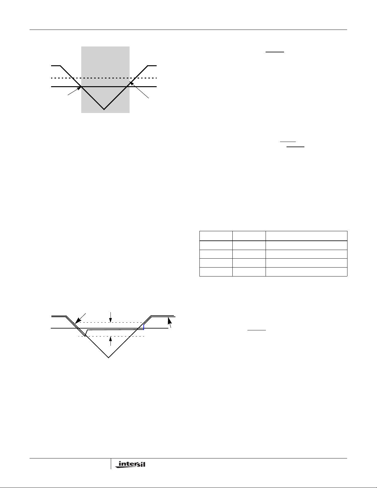
These two power control situations are illustrated in Figures
13 and 14.
BATTERY BACKUP
MODE
V
BAT
+ V
2.2V
1.8V
BATHYS
V
V
TRIP
V
BAT
DD
V
BAT
- V
BATHYS
- Option 1 - Standard Mode
- Option 2 - Legacy Mode (Default)
Note that the I
2
C bus may or may not be operational during
battery backup, that function is controlled by the SBIB bit.
That operation is covered after the power control section.
14
FIGURE 13. BATTERY SWITCHOVER WHEN V
< V
BAT
TRIP
FN6206.1
February 9, 2006
Page 15
BATTERY BACKUP
V
DD
V
BAT
V
TRIP
V
TRIP
FIGURE 14. BATTERY SWITCHOVER WHEN V
MODE
V
TRIP
+ V
BAT
3.0V
2.2V
TRIPHYS
> V
TRIP
OPTION 2 - LEGACY POWER CONTROL MODE
(DEFAULT)
The Legacy Mode follows conditions set in X1226 products.
In this mode, switching from VDD to VBAT is simply done by
comparing the voltages and the device operates from
whichever is the higher voltage.
To select the Option 2, BSW bit in the Power Register must
be set to “BSW = 1”
• Normal Mode (V
To transition from the V
) to Battery Backup Mode (V
DD
DD
to V
mode, the following
BAT
BAT
)
conditions must be met:
V
< V
DD
• Battery Backup Mode (V
The device will switch from the V
BAT
- V
BATHYS
) to Normal Mode (VDD)
BAT
to VDD mode when the
BAT
following condition occurs:
V
> V
DD
BAT +VBATHYS
The Legacy Mode power control conditions are illustrated in
Figure 15.
V
DD
V
BAT
OFF
FIGURE 15. BATTERY SWITCHOVER IN LEGACY MODE
VOLTAGE
ON
IN
ISL12029
Power-on Reset
Application of power to the ISL12029 activates a Power-on
Reset Circuit that pulls the RESET
pin active. This signal
provides several benefits.
- It prevents the system microprocessor from starting to
operate with insufficient voltage.
- It prevents the processor from operating prior to
stabilization of the oscillator.
- It allows time for an FPGA to download its configuration
prior to initialization of the circuit.
- It prevents communication to the EEPROM, greatly
reducing the likelihood of data corruption on power up.
When VDD exceeds the device V
typically 250ms the circuit releases RESET
threshold value for
RESET
, allowing the
system to begin operation. Recommended slew rate is
between 0.2V/ms and 50V/ms.
Watchdog Timer Operation
The watchdog timer timeout period is selectable. By writing a
value to WD1 and WD0, the watchdog timer can be set to 3
different time out periods or off. When the Watchdog timer is
set to off, the watchdog circuit is configured for low power
operation (See Table 7).
TABL E 7 .
WD1 WD0
1 1 disabled
1 0 250ms
0 1 750ms
0 0 1.75s
DURATION
Watchdog Timer Restart
The Watchdog Timer is started by a falling edge of SDA
when the SCL line is high (START condition). The start
signal restarts the watchdog timer counter, resetting the
period of the counter back to the maximum. If another
START fails to be detected prior to the watchdog timer
expiration, then the RESET
time out period. In the event that the start signal occurs
during a reset time out period, the start will have no effect.
When using a single START to refresh watchdog timer, a
STOP condition should be followed to reset the device back
to stand-by mode. See Figure 3.
pin becomes active for one reset
15
FN6206.1
February 9, 2006
Page 16
ISL12029
Low Voltage Reset (LVR) Operation
When a power failure occurs, a voltage comparator
compares the level of the V
voltage (V
below V
V
V
RESET
line rises above V
DD
, then the RESET output will remain asserted low.
RESET
), then generates a RESET pulse if it is
RESET
. The reset pulse will timeout 250ms after the
line versus a preset threshold
DD
. If the VDD remains below
RESET
Power up and power down waveforms are shown in
Figure 4. The LVR circuit is to be designed so the RESET
signal is valid down to V
DD
=1.0V.
When the LVR signal is active, unless the part has been
switched into the battery mode
, the completion of an in-
progress nonvolatile write cycle is unaffected, allowing a
nonvolatile write to continue as long as possible (down to the
Reset Valid Voltage). The LVR signal, when active, will
terminate any in-progress communications to the device and
prevents new commands from disrupting any current write
operations. See “I
2
C Communications During Battery backup
and LVR Operation”.
Serial Communication
The device supports the I2C bidirectional serial bus protocol.
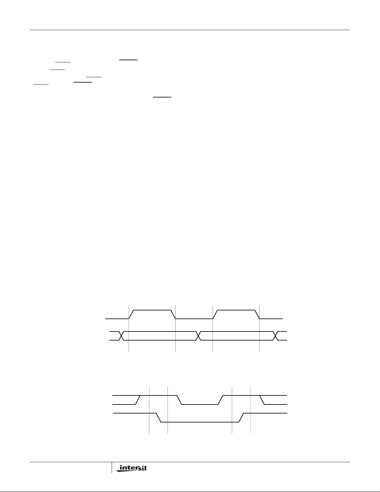
CLOCK AND DATA
Data states on the SDA line can change only during SCL
LOW. SDA state changes during SCL HIGH are reserved for
indicating start and stop conditions. See Figure 16.
START CONDITION
All commands are preceded by the start condition, which is a
HIGH to LOW transition of SDA when SCL is HIGH. The
device continuously monitors the SDA and SCL lines for the
start condition and will not respond to any command until
this condition has been met. See Figure 17.
STOP CONDITION
All communications must be terminated by a stop condition,
which is a LOW to HIGH transition of SDA when SCL is
HIGH. The stop condition is also used to place the device
into the Standby power mode after a read sequence. A stop
condition can only be issued after the transmitting device
has released the bus. See Figure 17.
ACKNOWLEDGE
Acknowledge is a software convention used to indicate
successful data transfer. The transmitting device, either
master or slave, will release the bus after transmitting eight
bits. During the ninth clock cycle, the receiver will pull the
SDA line LOW to acknowledge that it received the eight bits of
data. Refer to Figure 18.
The device will respond with an acknowledge after
recognition of a start condition and if the correct Device
Identifier and Select bits are contained in the Slave Address
Byte. If a write operation is selected, the device will respond
with an acknowledge after the receipt of each subsequent
eight bit word. The device will not acknowledge if the slave
address byte is incorrect.
In the read mode, the device will transmit eight bits of data,
release the SDA line, then monitor the line for an
acknowledge. If an acknowledge is detected and no stop
condition is generated by the master, the device will continue
to transmit data. The device will terminate further data
transmissions if an acknowledge is not detected. The master
must then issue a stop condition to return the device to
Standby mode and place the device into a known state.
SCL
SDA
SCL
SDA
16
DATA STABLE DATA CHANGE DATA STABLE
FIGURE 16. VALID DATA CHANGES ON THE SDA BUS
START
FIGURE 17. VALID START AND STOP CONDITIONS
STOP
FN6206.1
February 9, 2006
Page 17
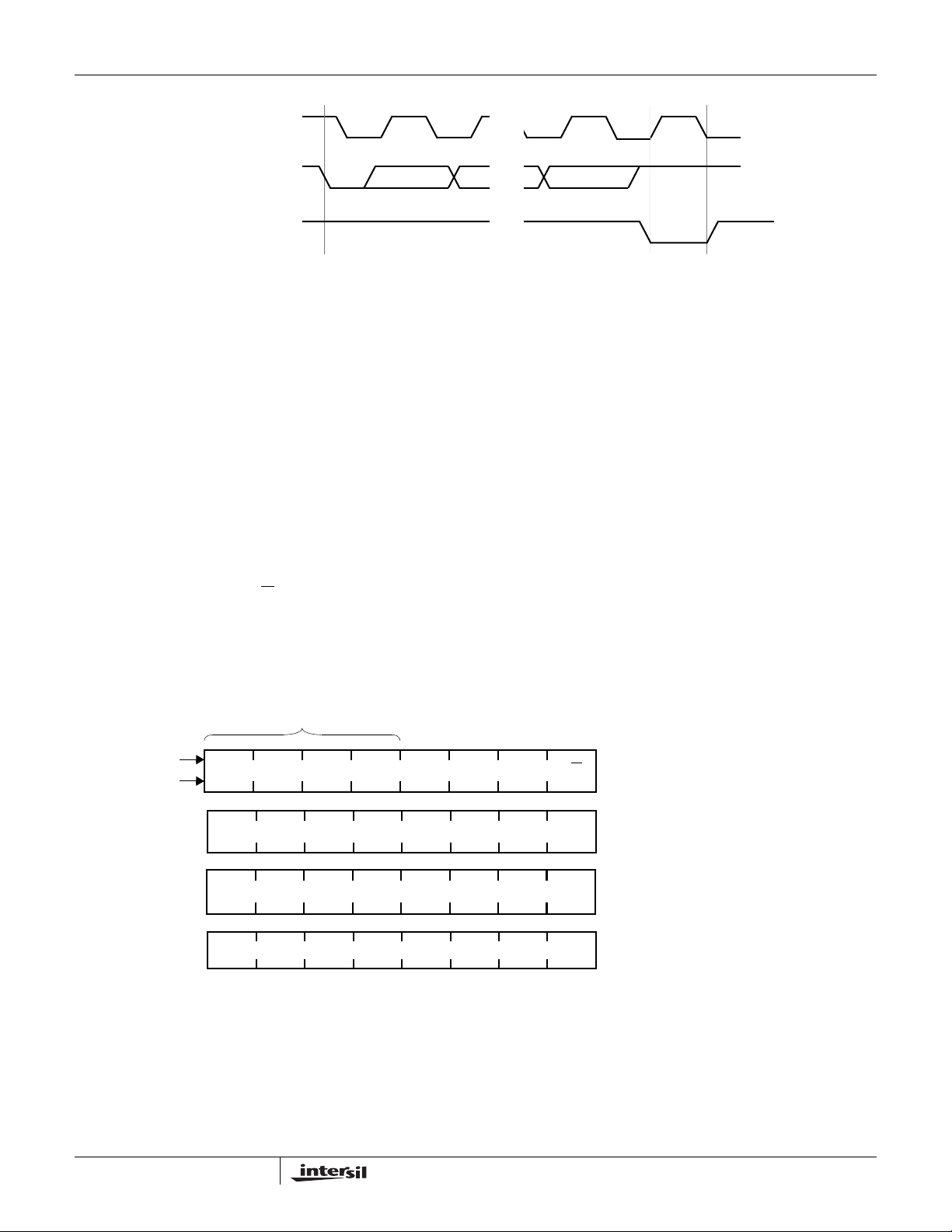
SCL FROM
MASTER
DATA OUTPUT
FROM TRANSMITTER
DATA OUTPUT
FROM RECEIVER
ISL12029
1
START ACKNOWLEDGE
8
FIGURE 18. ACKNOWLEDGE RESPONSE FROM RECEIVER
9
Device Addressing
Following a start condition, the master must output a Slave
Address Byte. The first four bits of the Slave Address Byte
specify access to either the EEPROM array or to the CCR.
Slave bits ‘1010’ access the EEPROM array. Slave bits
‘1101’ access the CCR.
When shipped from the factory, EEPROM array is
UNDEFINED, and should be programmed by the customer
to a known state.
Bit 3 through Bit 1 of the slave byte specify the device select
bits. These are set to ‘111’.
The last bit of the Slave Address Byte defines the operation
to be performed. When this R/W
operation is selected. A zero selects a write operation. Refer
to Figure 19.
After loading the entire Slave Address Byte from the SDA
bus, the ISL12029 compares the device identifier and device
Array
CCR
1
1
bit is a one, then a read
DEVICE IDENTIFIER
0
1
1
0
0
1
1
select bits with ‘1010111’ or ‘1101111’. Upon a correct
compare, the device outputs an acknowledge on the SDA
line.
Following the Slave Byte is a two byte word address. The
word address is either supplied by the master device or
obtained from an internal counter. On power up the internal
address counter is set to address 0h, so a current address
read of the EEPROM array starts at address 0. When
required, as part of a random read, the master must supply
the 2 Word Address Bytes as shown in Figure 19.
In a random read operation, the slave byte in the “dummy
write” portion must match the slave byte in the “read”
section. That is if the random read is from the array the slave
byte must be 1010111x in both instances. Similarly, for a
random read of the Clock/Control Registers, the slave byte
must be 1101111x in both places.
1
1
R/W
SLAVE ADDRESS BYTE
BYTE 0
00 0 0 0A80
A6 A5
D7 D6 D5 D2D4 D3 D1 D0
0
A0A7 A2A4 A3 A1
WORD ADDRESS 1
BYTE 1
WORD ADDRESS 0
BYTE 2
DATA BYTE
BYTE 3
FIGURE 19. SLAVE ADDRESS, WORD ADDRESS, AND DATA BYTES (64 BYTE PAGES)
17
FN6206.1
February 9, 2006
Page 18
ISL12029
Write Operations
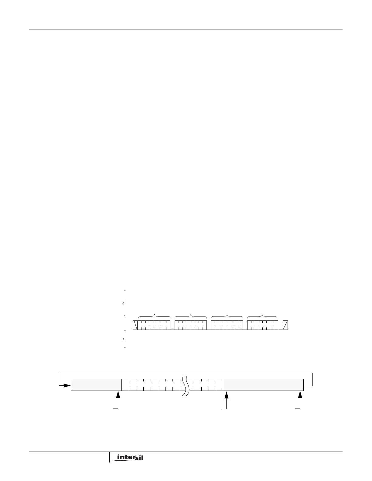
BYTE WRITE
For a write operation, the device requires the Slave Address
Byte and the Word Address Bytes. This gives the master
access to any one of the words in the array or CCR. (Note:
Prior to writing to the CCR, the master must write a 02h, then
06h to the status register in two preceding operations to
enable the write operation. See “Writing to the Clock/Control
Registers.”) Upon receipt of each address byte, the
ISL12029 responds with an acknowledge. After receiving
both address bytes the ISL12029 awaits the eight bits of
data. After receiving the 8 data bits, the ISL12029 again
responds with an acknowledge. The master then terminates
the transfer by generating a stop condition. The ISL12029
then begins an internal write cycle of the data to the
nonvolatile memory. During the internal write cycle, the
device inputs are disabled, so the device will not respond to
any requests from the master. The SDA output is at high
impedance. See Figure 20.
A write to a protected block of memory is ignored, but will still
receive an acknowledge. At the end of the write command,
the ISL12029 will not initiate an internal write cycle, and will
continue to ACK commands.
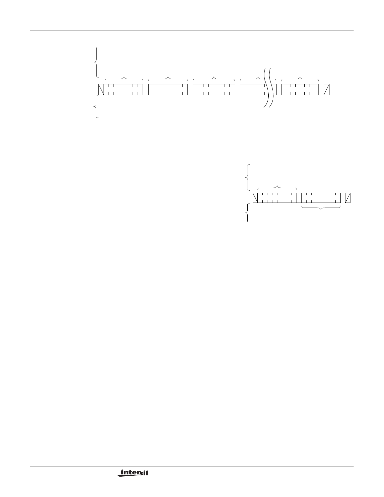
PAGE WRITE
The ISL12029 has a page write operation. It is initiated in the
same manner as the byte write operation; but instead of
terminating the write cycle after the first data byte is
transferred, the master can transmit up to 15 more bytes to
the memory array and up to 7 more bytes to the clock/control
registers. The RTC registers require a page write (8 bytes),
individual register writes are not allowed. (Note: Prior to
writing to the CCR, the master must write a 02h, then 06h to
the status register in two preceding operations to enable the
write operation. See “Writing to the Clock/Control
Registers.”)
After the receipt of each byte, the ISL12029 responds with
an acknowledge, and the address is internally incremented
by one. The address pointer remains at the last address byte
written. When the counter reaches the end of the page, it
“rolls over” and goes back to the first address on the same
page. This means that the master can write 16 bytes to a
memory array page or 8 bytes to a CCR section starting at
any location on that page. For example, if the master begins
writing at location 10 of the memory and loads 15 bytes, then
the first 6 bytes are written to addresses 10 through 15, and
the last 6 bytes are written to columns 0 through 5.
Afterwards, the address counter would point to location 6 on
the page that was just written. If the master supplies more
than the maximum bytes in a page, then the previously
loaded data is over-written by the new data, one byte at a
time. Refer to Figure 21.The master terminates the Data
Byte loading by issuing a stop condition, which causes the
ISL12029 to begin the nonvolatile write cycle. As with the
byte write operation, all inputs are disabled until completion
of the internal write cycle. Refer to Figure 22 for the address,
acknowledge, and data transfer sequence.
STOPS AND WRITE MODES
Stop conditions that terminate write operations must be sent
by the master after sending at least 1 full data byte and it’s
associated ACK signal. If a stop is issued in the middle of a
data byte, or before 1 full data byte + ACK is sent, then the
ISL12029 resets itself without performing the write. The
contents of the array are not affected.
S
SIGNALS FROM
THE MASTER
SDA BUS
SIGNALS FROM
THE SLAVE
6 BYTES
ADDRESS=5
ADDRESS POINTER ENDS
AT ADDR= 5
.
FIGURE 21. WRITING 12 BYTES TO A 16-BYTE MEMORY PAGE STARTING AT ADDRESS 10
18
T
A
SLAVE
R
T
ADDRESS
1111
FIGURE 20. BYTE WRITE SEQUENCE
WORD
ADDRESS 1
0
0000000
A
C
K
ADDRESS
WORD
ADDRESS 0
A
C
K
10
A
C
K
6 BYTES
DATA
S
T
O
P
A
C
K
ADDRESS
15
FN6206.1
February 9, 2006
Page 19
ISL12029
S
SIGNALS FROM
THE MASTER
SDA BUS
SIGNALS FROM
THE SLAVE
T
A
R
T
SLAVE
ADDRESS
0
1111
0000000
A
C
K
WORD
ADDRESS 1
FIGURE 22. PAGE WRITE SEQUENCE
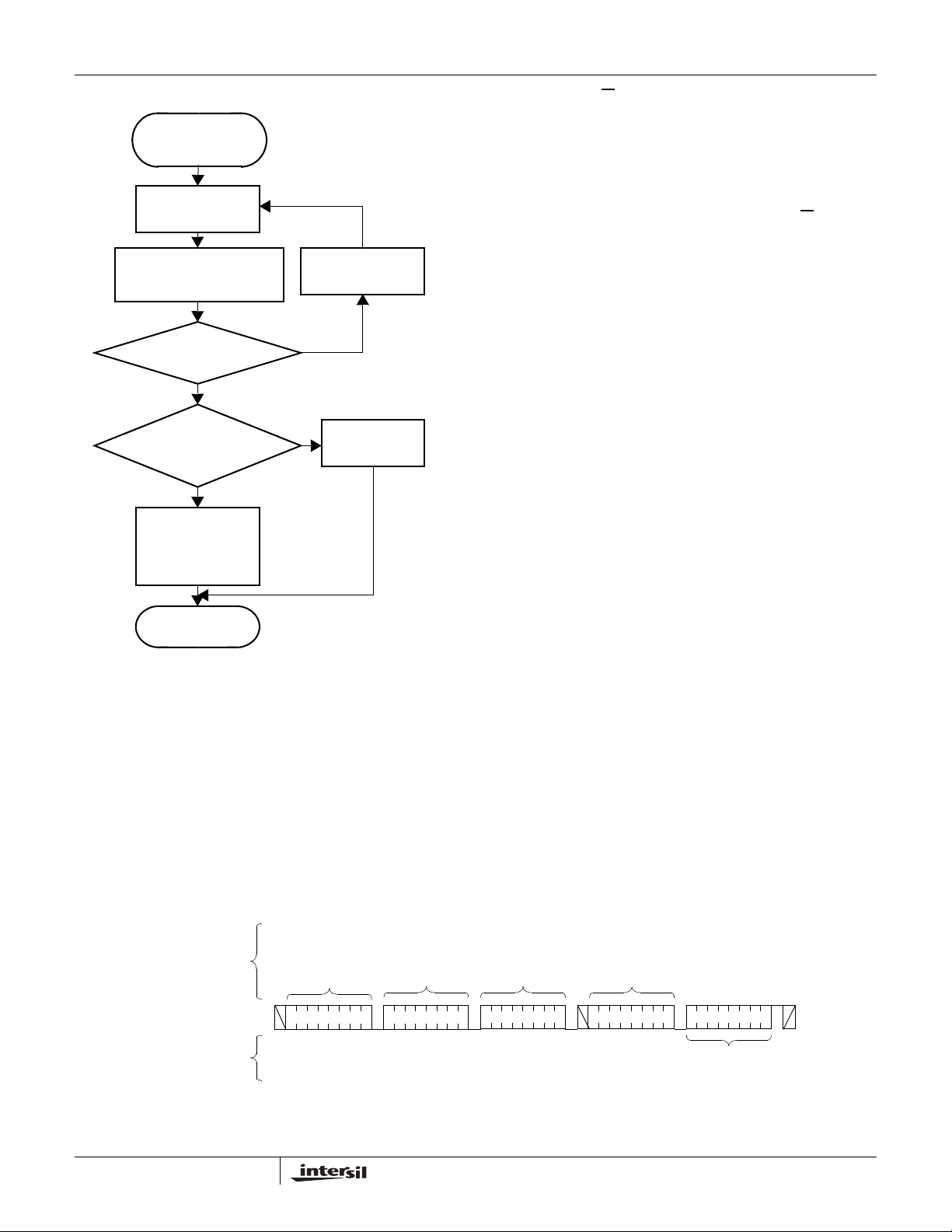
ACKNOWLEDGE POLLING
Disabling of the inputs during nonvolatile write cycles can be
used to take advantage of the typical 5ms write cycle time.
Once the stop condition is issued to indicate the end of the
master’s byte load operation, the ISL12029 initiates the
internal nonvolatile write cycle. Acknowledge polling can
begin immediately. To do this, the master issues a start
condition followed by the Memory Array Slave Address Byte
for a write or read operation (AEh or AFh). If the ISL12029 is
still busy with the nonvolatile write cycle then no ACK will be
returned. When the ISL12029 has completed the write
operation, an ACK is returned and the host can proceed with
the read or write operation. Refer to the flow chart in
Figure 24. Note: Do not use the CCR Slave byte (DEh or
DFh) for Acknowledge Polling.
A
C
K
ADDRESS 0
1 ≤ n ≤ 16 for EEPROM array
1 ≤ n ≤ 8 for CCR
WORD
SIGNALS FROM
THE MASTER
SDA BUS
SIGNALS FROM
THE SLAVE
DATA
(1)
A
C
K
S
T
SLAVE
A
R
ADDRESS
T
DATA
11111
(n)
A
C
DATA
K
FIGURE 23. CURRENT ADDRESS READ SEQUENCE
S
T
O
P
A
C
K
S
T
O
P
READ OPERATIONS
There are three basic read operations: Current Address
Read, Random Read, and Sequential Read.
Current Address Read
Internally the ISL12029 contains an address counter that
maintains the address of the last word read incremented by
one. Therefore, if the last read was to address n, the next
read operation would access data from address n+1. On
power up, the sixteen bit address is initialized to 0h. In this
way, a current address read immediately after the power-on
reset can download the entire contents of memory starting at
the first location.Upon receipt of the Slave Address Byte with
the R/W
acknowledge, then transmits eight data bits. The master
terminates the read operation by not responding with an
acknowledge during the ninth clock and issuing a stop
condition. Refer to Figure 23 for the address, acknowledge,
and data transfer sequence.
bit set to one, the ISL12029 issues an
19
FN6206.1
February 9, 2006
Page 20
ISL12029
Byte load completed
by issuing STOP.
Enter ACK Polling
Issue START
Issue Memory Array Slave
Address Byte
AFh (Read) or AEh (Write)
ACK
returned?
YES
nonvolatile write
Cycle complete. Continue
command sequence?
YES
Continue normal
Read or Write
command
sequence
PROCEED
Issue STOP
NO
NO
Issue STOP
FIGURE 24. ACKNOWLEDGE POLLING SEQUENCE
Byte with the R/W
bit set to zero, the master must first
perform a “dummy” write operation.
The master issues the start condition and the slave address
byte, receives an acknowledge, then issues the word
address bytes. After acknowledging receipt of each word
address byte, the master immediately issues another start
condition and the slave address byte with the R/W
bit set to
one. This is followed by an acknowledge from the device and
then by the eight bit data word. The master terminates the
read operation by not responding with an acknowledge and
then issuing a stop condition. Refer to Figure 25 for the
address, acknowledge, and data transfer sequence.
In a similar operation called “Set Current Address,” the
device sets the address if a stop is issued instead of the
second start shown in Figure 25. The ISL12029 then goes
into standby mode after the stop and all bus activity will be
ignored until a start is detected. This operation loads the new
address into the address counter. The next Current Address
Read operation will read from the newly loaded address.
This operation could be useful if the master knows the next
address it needs to read, but is not ready for the data.
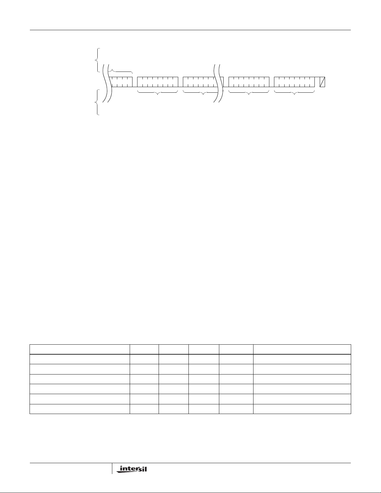
SEQUENTIAL READ
Sequential reads can be initiated as either a current address
read or random address read. The first data byte is
transmitted as with the other modes; however, the master
now responds with an acknowledge, indicating it requires
additional data. The device continues to output data for each
acknowledge received. The master terminates the read
operation by not responding with an acknowledge and then
issuing a stop condition.
It should be noted that the ninth clock cycle of the read
operation is not a “don’t care.” To terminate a read operation,
the master must either issue a stop condition during the
ninth cycle or hold SDA HIGH during the ninth clock cycle
and then issue a stop condition.
RANDOM READ
Random read operations allow the master to access any
location in the ISL12029. Prior to issuing the Slave Address
S
SIGNALS FROM
THE MASTER
SDA BUS
SIGNALS FROM
THE SLAVE
T
A
R
T
SLAVE
ADDRESS
1111
ADDRESS 1
0
0000000
A
C
K
WORD
FIGURE 25. RANDOM ADDRESS READ SEQUENCE
The data output is sequential, with the data from address n
followed by the data from address n + 1. The address
counter for read operations increments through all page and
column addresses, allowing the entire memory contents to
be serially read during one operation. At the end of the
address space the counter “rolls over” to the start of the
address space and the ISL12029 continues to output data
for each acknowledge received. Refer to Figure 26 for the
acknowledge and data transfer sequence.
S
ADDRESS 0
A
C
K
WORD
A
C
K
T
A
R
T
SLAVE
ADDRESS
1111
1
A
C
K
DATA
S
T
O
P
20
FN6206.1
February 9, 2006
Page 21
ISL12029
SIGNALS FROM
THE MASTER
SDA BUS
SIGNALS FROM
THE SLAVE
SLAVE
ADDRESS
1
A
C
K
DATA
(1)
FIGURE 26. SEQUENTIAL READ SEQUENCE
Application Section
Crystal Oscillator and Temperature Compensation
Intersil has now integrated the oscillator compensation
circuity on-chip, to eliminate the need for external
components and adjust for crystal drift over temperature and
enable very high accuracy time keeping (<5ppm drift).
The Intersil RTC family uses an oscillator circuit with on-chip
crystal compensation network, including adjustable loadcapacitance. The only external component required is the
crystal. The compensation network is optimized for operation
with certain crystal parameters which are common in many
of the surface mount or tuning-fork crystals available today.
Table 8 summarizes these parameters.
Table 9 contains some crystal manufacturers and part
numbers that meet the requirements for the Intersil RTC
products.
The turnover temperature in Table 8 describes the
temperature where the apex of the of the drift vs.
temperature curve occurs. This curve is parabolic with the
drift increasing as (T-T0)
example, the turnover temperature is typically 25°C, and a
peak drift of >110ppm occurs at the temperature extremes of
2
. For an Epson MC-405 device, for
A
C
K
DATA
(2)
A
C
K
DATA
(n-1)
(n is any integer greater than 1)
A
C
K
DATA
(n)
S
T
O
P
-40 and +85°C. It is possible to address this variable drift by
adjusting the load capacitance of the crystal, which will result
in predictable change to the crystal frequency. The Intersil
RTC family allows this adjustment over temperature since
the devices include on-chip load capacitor trimming. This
control is handled by the Analog Trimming Register, or ATR,
which has 6 bits of control. The load capacitance range
covered by the ATR circuit is approximately 3.25pF to
18.75pF, in 0.25pF increments. Note that actual capacitance
would also include about 2pF of package related
capacitance. In-circuit tests with commercially available
crystals demonstrate that this range of capacitance allows
frequency control from +116ppm to -37ppm, using a 12.5pF
load crystal.
In addition to the analog compensation afforded by the
adjustable load capacitance, a digital compensation feature
is available for the Intersil RTC family. There are three bits
known as the Digital Trimming Register or DTR, and they
operate by adding or skipping pulses in the clock signal. The
range provided is ±30ppm in increments of 10ppm. The
default setting is 0ppm. The DTR control can be used for
coarse adjustments of frequency drift over temperature or for
crystal initial accuracy correction.
TABLE 8. CRYSTAL PARAMETERS REQUIRED FOR INTERSIL RTCs
PARAMETER MIN TYP MAX UNITS NOTES
Frequency 32.768 kHz
Frequency Tolerance ±100 ppm Down to 20ppm if desired
Turnover Temperature 20 25 30 °C Typically the value used for most crystals
Operating Temperature Range -40 85 °C
Parallel Load Capacitance 12.5 pF
Equivalent Series Resistance 50 k
21
Ω For best oscillator performance
FN6206.1
February 9, 2006
Page 22
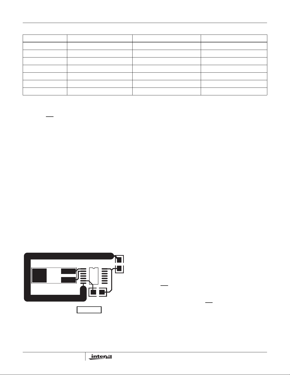
ISL12029
TABLE 9. CRYSTAL MANUFACTURERS
MANUFACTURER PART NUMBER TEMP RANGE (°C) +25°C FREQUENCY TOLERANCE
Citizen CM201, CM202, CM200S -40 to +85 ±20ppm
Epson MC-405, MC-406 -40 to +85 ±20ppm
Raltron RSM-200S-A or B -40 to +85 ±20ppm
SaRonix 32S12A or B -40 to +85 ±20ppm
Ecliptek ECPSM29T-32.768K -10 to +60 ±20ppm
ECS ECX-306/ECX-306I -10 to +60 ±20ppm
Fox FSM-327 -40 to +85 ±20ppm
A final application for the ATR control is in-circuit calibration
for high accuracy applications, along with a temperature
sensor chip. Once the RTC circuit is powered up with battery
backup, the IRQ
/F
output is set at 32.768kHz and
OUT
frequency drift is measured. The ATR control is then
adjusted to a setting which minimizes drift. Once adjusted at
a particular temperature, it is possible to adjust at other
discrete temperatures for minimal overall drift, and store the
resulting settings in the EEPROM. Extremely low overall
temperature drift is possible with this method. The Intersil
evaluation board contains the circuitry necessary to
implement this control.
For more detailed operation see Intersil’s application note
AN154 on Intersil’s website at www.intersil.com.
Layout Considerations
The crystal input at X1 has a very high impedance and will
pick up high frequency signals from other circuits on the
board. Since the X2 pin is tied to the other side of the crystal,
it is also a sensitive node. These signals can couple into the
oscillator circuit and produce double clocking or misclocking, seriously affecting the accuracy of the RTC. Care
needs to be taken in layout of the RTC circuit to avoid noise
pickup. Figure 27 shows a suggested layout for the
ISL12029 or ISL12028 devices.
C1
0.1µF
The X1 and X2 connections to the crystal are to be kept as
short as possible. A thick ground trace around the crystal is
advised to minimize noise intrusion, but ground near the X1
and X2 pins should be avoided as it will add to the load
capacitance at those pins. Keep in mind these guidelines for
other PCB layers in the vicinity of the RTC device. A small
decoupling capacitor at the V
pin of the chip is mandatory,
DD
with a solid connection to ground.
For other RTC products, the same rules stated above should
be observed, but adjusted slightly since the packages and
pinouts are slightly different.
Oscillator Measurements
When a proper crystal is selected and the layout guidelines
above are observed, the oscillator should start up in most
circuits in less than one second. Some circuits may take slightly
longer, but startup should definitely occur in less than 5
seconds. When testing RTC circuits, the most common impulse
is to apply a scope probe to the circuit at the X2 pin (oscillator
output) and observe the waveform. DO NOT DO THIS!
Although in some cases you may see a usable waveform, due
to the parasitics (usually 10pF to ground) applied with the
scope probe, there will be no useful information in that
waveform other than the fact that the circuit is oscillating. The
X2 output is sensitive to capacitive impedance so the voltage
levels and the frequency will be affected by the parasitic
elements in the scope probe. Applying a scope probe can
possibly cause a faulty oscillator to start up, hiding other issues
(although in the Intersil RTCs, the internal circuitry assures
startup when using the proper crystal and layout).
R1 10k
XTAL1
32.768kGz
FIGURE 27. SUGGESTED LAYOUT FOR INTERSIL RTC IN
SO-14
U1
ISL12029
X1228
22
The best way to analyze the RTC circuit is to power it up and
read the real time clock as time advances, or if the chip has
the IRQ
/F
output, look at the output of that pin on an
OUT
oscilloscope (after enabling it with the control register, and
using a pull-up resistor for the open-drain output).
Alternatively, the ISL12029 IRQ
/F
- output can be
OUT
checked by setting an alarm for each minute. Using the
pulse interrupt mode setting, the once-per-minute interrupt
functions as an indication of proper oscillation.
FN6206.1
February 9, 2006
Page 23
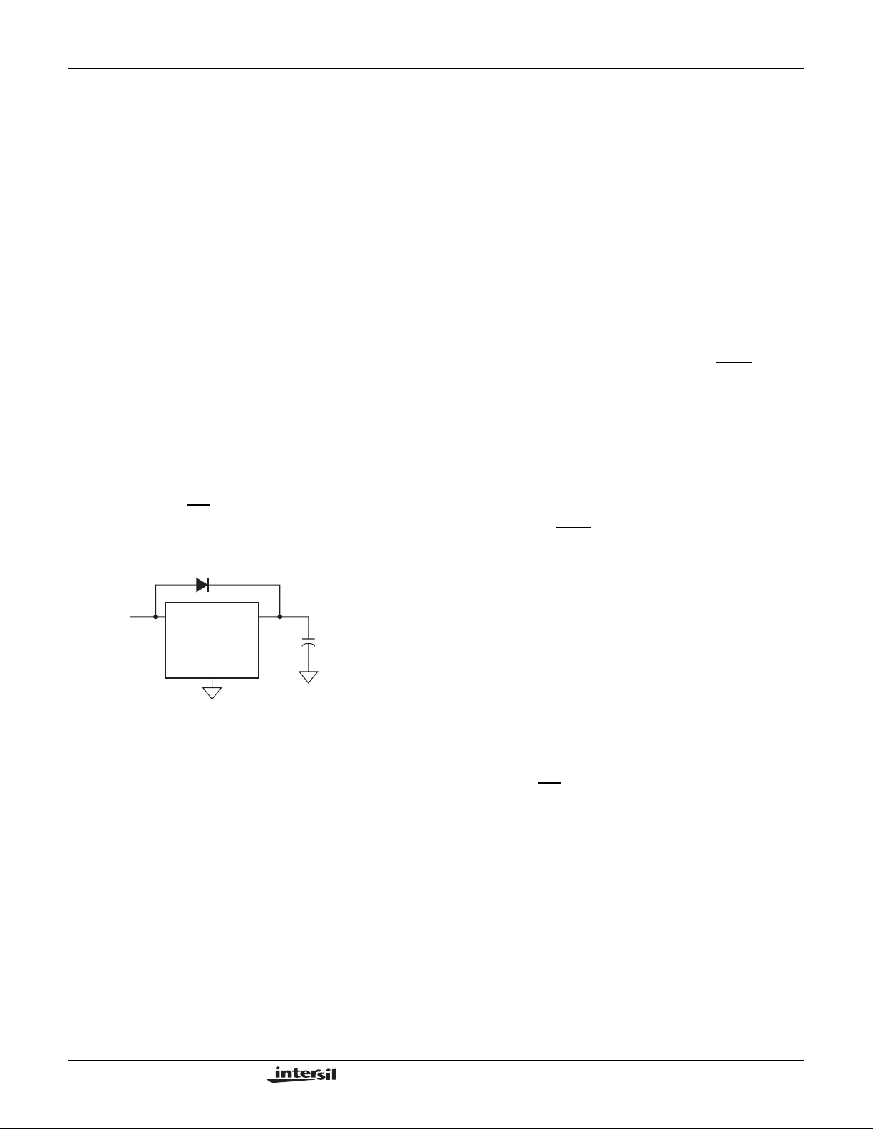
ISL12029
Backup Battery Operation
Many types of batteries can be used with the Intersil RTC
products. 3.0V or 3.6V Lithium batteries are appropriate, and
sizes are available that can power a Intersil RTC device for up
to 10 years. Another option is to use a supercapacitor for
applications where V
periods of time. Depending on the value of supercapacitor
used, backup time can last from a few days to two weeks (with
>1F). A simple silicon or Schottky barrier diode can be used in
series with V
DD
connected to the V
very low leakages, <1µA desireable. Do not use the diode to
charge a battery (especially lithium batteries!).
There are two possible modes for battery backup operation,
Standard and Legacy mode. In Standard mode, there are no
operational concerns when switching over to battery backup
since all other devices functions are disabled. Battery drain
is minimal in Standard mode, and return to Normal V
powered operationis predicatable. In Legacy modes the
V
pin can power the chip if the voltage is above V
BAT
V
This makes it possible to generate alarms and
TRIP .
communicate with the device under battery backup, but the
supply current drain is much higher than the Standard mode
and backup time is reduced. In this case if alarms are used
in backup mode, the IRQ
connected to V
BAT
the default mode is the Sandard mode.
2.7-5.5V
FIGURE 28. SUPERCAPACITOR CHARGING CIRCUIT
may disappear intermittently for short
DD
to charge the supercapacitor, which is
pin. Try to use Schottky diodes with
BAT
/F
pull up resistor must be
OUT
voltage source. During initial power-up
V
CC
V
back
Supercapacitor
V
SS
DD
DD
and
I2C Communications During Battery Backup and
LVR Operation
Operation in Battery Backup mode and LVR is affected by
the BSW and SBIB bits as described earlier. These bits allow
flexible operation of the serial bus and EEPROM in battery
backup mode, but certain operational details need to be
clear before utilizing the different modes. The most
significant detail is that once VDD goes below VRESET, then
2
I
C communications cease regardless of whether the device
is programmed for I
Table 10 describes 4 different modes possible with using the
BSW and SBIB bits, and how they are affect LVR and battery
backup operation.
• Mode A - In this mode selection bits indicate a low VDD
switchover combined with I
mode. In actuality the VDD will go below V
switching to battery backup, which will disable I2C
ANYTIME the device goes into battery backup mode.
Regardless of the battery voltage, the I
to the V
RESET
• Mode B - In this mode the selection bits indicate
switchover to battery backup at V
communications in battery backup. In order to
communicate in battery backup mode, the V
must be less than the VBAT voltage AND V
greater than V
must go to V
as the normal operating mode of the X1228 device
• Mode C - In this mode the selection bits indicate a low
VDD switchover combined with no communications in
battery backup. Operation is actually identical to Mode A
2
C communications down to VDD=V
with I
communications (see Figure 29).
• Mode D - In this mode the selection bits indicate
switchover to battery backup at V
communications in battery backup. This mode is unique in
that there is I
than VRESET or VBAT, whichever is greater. This mode is
the safest for guaranteeing I
there is a Valid V
Note that the IRQ
backup for all modes. This should be considered if the load
on this pin is powered down, and could draw current from
the PMOS transistor and drain the battery. If that is the case,
the designer should consider the ISL12029 device which has
an open-drain output and avoids excessive curent draw in
battery backup.
2
C operation in battery backup mode.
2
C operation in battery backup
before
RESET
2
C will work down
voltage (See Figure 29).
DD<VBAT
. Also, pullups on the I2C bus pins
RESET
to communicate. This mode is the same
BAT
DD<VBAT
2
C communication as long as VDD is higher
2
C communications only when
. (see Figure 30)
DD
/F
CMOS output pin is active in battery
OUT
, and I2C
voltage
RESET
must be
DD
, then no
RESET
, and no I2C
23
FN6206.1
February 9, 2006
Page 24
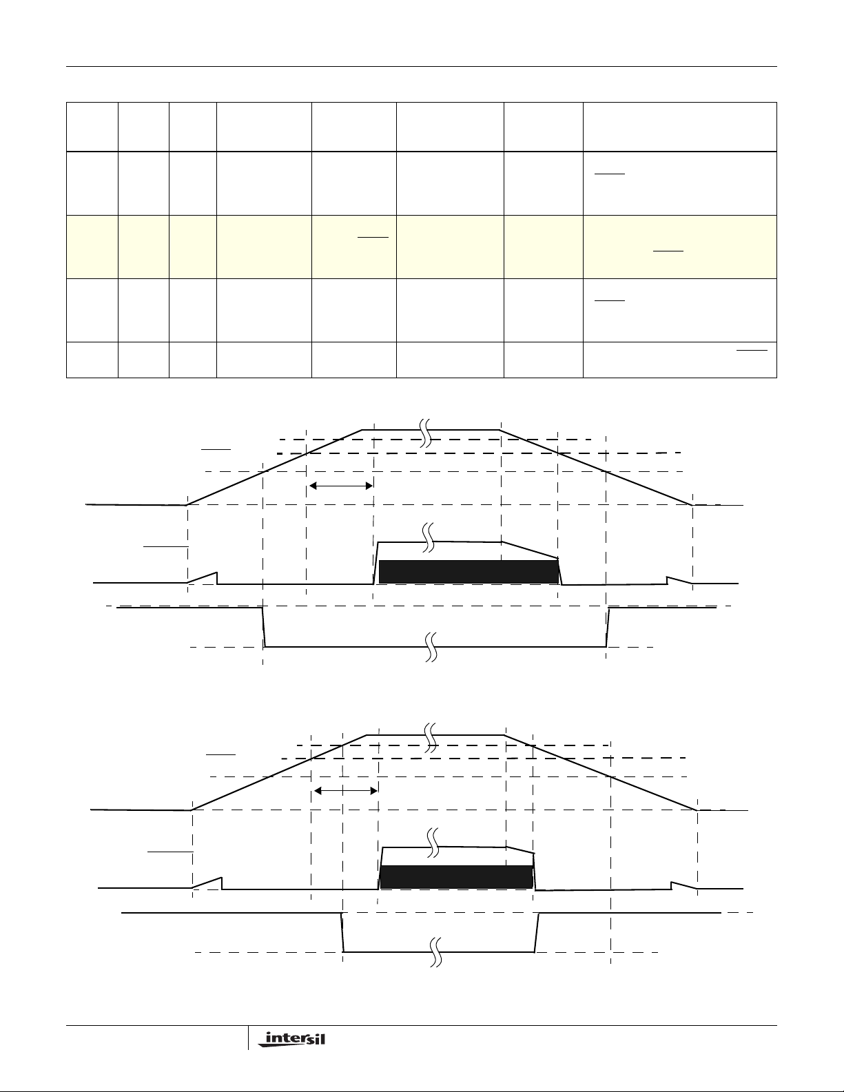
ISL12029
TABLE 10. I2C, LV RESET, AND BATTERY BACKUP OPERATION SUMMARY (SHADED ROW IS SAME AS X1228 OPERATION)
2
VBAT
SWITCHOVER
VOLTAGE
MODE
SBIB
BIT
BSW
BIT
A 0 0 Standard Mode,
V
= 2.2V typ
TRIP
B
(X1228
0 1 Legacy Mode,
V
< V
DD
mode)
C 1 0 Standard Mode,
V
= 2.2V typ
TRIP
D 1 1 Legacy Mode,
V
< V
DD
V
(3.0V)
V
DD
V
TRIP
(2.2V)
V
RESET
BAT
(2.63V)
BAT
BAT
I
C ACTIVE IN
BATTERY
BACKUP?
NO NO YES Operation of I
YES, only if
V
BAT>VRESET
NO NO YES Operation of I2C bus down to VDD =
NO NO YES Operation of I2C busdown to V
tPURST
EE PROM WRITE/
READ IN BATTERY
BACKUP?
FREQ/IRQ
ACTIVE? NOTES
2
V
RESET
communications. Battery switchover
at V
TRIP
C bus down to VDD =
, then below that no
.
YES YES Operation of I2C bus into battery
backup mode, but only for
V
BAT>VDD>VRESET
Bus must have pullups to V
V
, then below that no
RESET
communications. Battery switchover
at V
.
TRIP
or V
, whichever is higher.
BAT
.
BAT
.
RESET
RESET
I
BAT
V
DD
RESET
I
BAT
V
TRIP
(2.2V)
I2C Bus Active
(VDD power, V
not connected)
BAT
FIGURE 29. EXAMPLE RESET OPERATION IN MODE A OR C
V
(3.0V)
V
RESET
BAT
(2.63V)
tPURST
I2C Bus Active
(Battery backup mode)
(Battery backup mode)
24
FIGURE 30. RESET OPERATION IN MODE D
FN6206.1
February 9, 2006
Page 25
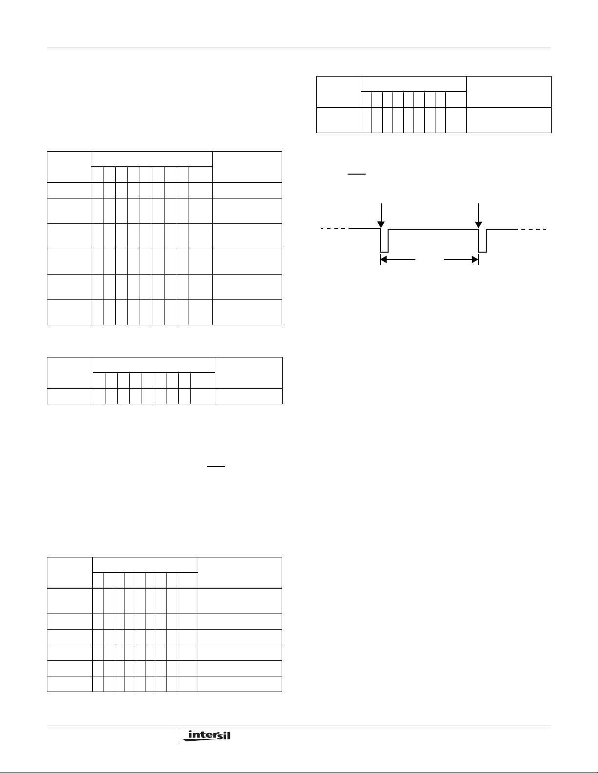
ISL12029
Alarm Operation Examples
Below are examples of both Single Event and periodic
Interrupt Mode alarms.
Example 1 – Alarm 0 set with single interrupt (IM = ”0”)
A single alarm will occur on January 1 at 11:30am.
A. Set Alarm 0 registers as follows:
ALARM0
REGISTER
SCA0 00000000 00hSeconds disabled
MNA0 10110000 B0hMinutes set to 30,
HRA0 10010001 91hHours set to 11,
DTA0 10000001 81hDate set to 1,
MOA0 10000001 81hMonth set to 1,
DWA0 00000000 00hDay of week
B. Also the AL0E bit must be set as follows:
BIT
DESCRIPTION76543210HEX
enabled
enabled
enabled
enabled
disabled
B. Set the Interrupt register as follows:
CONTROL
REGISTER
INT 1 0 1 x x 0 0 0 x0h Enable Alarm and Int
BIT
DESCRIPTION76543210HEX
Mode
XX indicate other control bits
Once the registers are set, the following waveform will be
seen at IRQ/
F
-:
OUT
RTC and alarm registers are both “30” sec
60 sec
Note that the status register AL0 bit will be set each time the
alarm is triggered, but does not need to be read or cleared.
CONTROL
REGISTER
INT 00100000 x0hEnable Alarm
BIT
DESCRIPTION76543210HEX
After these registers are set, an alarm will be generated when
the RTC advances to exactly 11:30am on January 1 (after
seconds changes from 59 to 00) by setting the AL0 bit in the
status register to “1” and also bringing the IRQ/
F
OUT
output
low.
Example 2 – Pulsed interrupt once per minute (IM = ”1”)
Interrupts at one minute intervals when the seconds register
is at 30 seconds.
A. Set Alarm 0 registers as follows:
ALARM0
REGISTER
SCA0 10110000B0hSeconds set to 30,
MNA0 0000000000hMinutes disabled
HRA0 00000000 00hHours disabled
DTA0 00000000 00hDate disabled
MOA0 00000000 00hMonth disabled
DWA0 00000000 00hDay of week disabled
BIT
DESCRIPTION76543210HEX
enabled
25
FN6206.1
February 9, 2006
Page 26
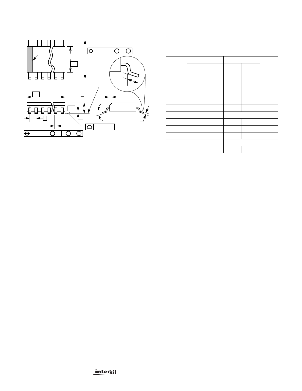
Small Outline Plastic Packages (SOIC)
ISL12029
N
INDEX
AREA
123
-A-
E
-B-
SEATING PLANE
D
A
-C-
0.25(0.010) BM M
H
L
h x 45
o
α
e
B
0.25(0.010) C AM BS
M
NOTES:
1. Symbols are defined in the “MO Series Symbol List” in Section 2.2 of
Publication Number 95.
2. Dimensioning and tolerancing per ANSI Y14.5M-1982.
3. Dimension “D” does not include mold flash, protrusions or gate burrs.
Mold flash, protrusion and gate burrs shall not exceed 0.15mm (0.006
inch) per side.
4. Dimension “E” does not include interlead flash or protrusions. Interlead
flash and protrusions shall not exceed 0.25mm (0.010 inch) per side.
5. The chamfer on the body is optional. If it is not present, a visual index
feature must be located within the crosshatched area.
6. “L” is the length of terminal for soldering to a substrate.
7. “N” is the number of terminal positions.
8. Terminal numbers are shown for reference only.
9. The lead width “B”, as measured 0.36mm (0.014 inch) or greater
above the seating plane, shall not exceed a maximum value of
0.61mm (0.024 inch).
10. Controlling dimension: MILLIMETER. Converted inch dimensions
are not necessarily exact.
A1
C
0.10(0.004)
M14.15 (JEDEC MS-012-AB ISSUE C)
14 LEAD NARROW BODY SMALL OUTLINE PLASTIC
PACKAGE
INCHES MILLIMETERS
SYMBOL
A 0.0532 0.0688 1.35 1.75 -
A1 0.0040 0.0098 0.10 0.25 -
B 0.013 0.020 0.33 0.51 9
C 0.0075 0.0098 0.19 0.25 D 0.3367 0.3444 8.55 8.75 3
E 0.1497 0.1574 3.80 4.00 4
e 0.050 BSC 1.27 BSC H 0.2284 0.2440 5.80 6.20 -
h 0.0099 0.0196 0.25 0.50 5
L 0.016 0.050 0.40 1.27 6
N14 147
o
α
0
o
8
o
0
o
8
Rev. 0 12/93
NOTESMIN MAX MIN MAX
-
26
FN6206.1
February 9, 2006
Page 27
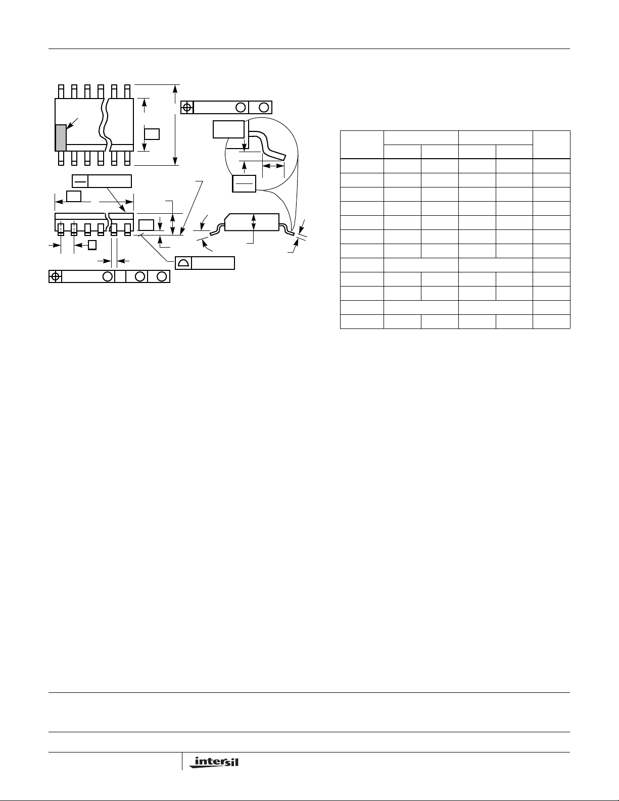
ISL12029
Thin Shrink Small Outline Plastic Packages (TSSOP)
N
INDEX
AREA
123
-A-
0.05(0.002)
D
SEATING PLANE
e
b
0.10(0.004) C AM BS
M
E1
-B-
A
-C-
0.25(0.010) BM M
E
α
A1
0.10(0.004)
GAUGE
PLANE
0.25
0.010
A2
L
c
NOTES:
1. These package dimensions are within allowable dimensions of
JEDEC MO-153-AC, Issue E.
2. Dimensioning and tolerancing per ANSI Y14.5M-1982.
3. Dimension “D” does not include mold flash, protrusions or gate burrs.
Mold flash, protrusion and gate burrs shall not exceed 0.15mm
(0.006 inch) per side.
4. Dimension “E1” does not include interlead flash or protrusions. Interlead flash and protrusions shall not exceed 0.15mm (0.006 inch) per
side.
5. The chamfer on the body is optional. If it is not present, a visual index
feature must be located within the crosshatched area.
6. “L” is the length of terminal for soldering to a substrate.
7. “N” is the number of terminal positions.
8. Terminal numbers are shown for reference only.
9. Dimension “b” does not include dambar protrusion. Allowable dambar
protrusion shall be 0.08mm (0.003 inch) total in excess of “b” dimension at maximum material condition. Minimum space between protrusion and adjacent lead is 0.07mm (0.0027 inch).
10. Controlling dimension: MILLIMETER. Converted inch dimensions
are not necessarily exact. (Angles in degrees)
M14.173
14 LEAD THIN SHRINK SMALL OUTLINE PLASTIC
PACKAGE
INCHES MILLIMETERS
SYMBOL
A - 0.047 - 1.20 A1 0.002 0.006 0.05 0.15 A2 0.031 0.051 0.80 1.05 -
b 0.0075 0.0118 0.19 0.30 9
c 0.0035 0.0079 0.09 0.20 -
D 0.195 0.199 4.95 5.05 3
E1 0.169 0.177 4.30 4.50 4
e 0.026 BSC 0.65 BSC -
E 0.246 0.256 6.25 6.50 -
L 0.0177 0.0295 0.45 0.75 6
N14 147
o
α
0
o
8
o
0
o
8
NOTESMIN MAX MIN MAX
-
Rev. 1 6/00
All Intersil U.S. products are manufactured, assembled and tested utilizing ISO9000 quality systems.
Intersil Corporation’s quality certifications can be viewed at www.intersil.com/design/quality
Intersil products are sold by description only. Intersil Corporation reserves the right to make changes in circuit design, software and/or specifications at any time without
notice. Accordingly, the reader is cautioned to verify that data sheets are current before placing orders. Information furnished by Intersil is believed to be accurate and
reliable. However, no responsibility is assumed by Intersil or its subsidiaries for its use; nor for any infringements of patents or other rights of third parties which may result
from its use. No license is granted by implication or otherwise under any patent or patent rights of Intersil or its subsidiaries.
For information regarding Intersil Corporation and its products, see www.intersil.com
27
FN6206.1
February 9, 2006
 Loading...