

Page 1

ISD1600 SERIES
SINGLE-MESSAGE
SINGLE-CHIP
6.6- TO 40-SECOND DURATION
VOICE RECORD/PLAYBACK DEVICE
Publication Release Date: November 4, 2004
- 1 - Revision 1
Page 2
ISD1600 SERIES
1. GENERAL DESCRIPTION
Winbond’s ISD1600 Series ChipCorder® is a single-message, single chip, record/playback solution
with selectable durations from 6.6 to 40 seconds. The CMOS device includes an on-chip oscillator (via
external control), microphone preamplifier, automatic gain control, anti-aliasing filter, Multi-Level
Storage (MLS) array, smoothing filter, PWM Class D speaker amplifier for standard 8Ω speaker or
buzzer, plus an extra current output. Recording is stored into the embedded Flash memory cells,
providing zero-power message storage. This unique single-chip solution ultilizes Winbond’s patented
MLS technology. Therefore, voice or audio data are stored directly into the memory in their natural
form without any compressions alike digital approach, providing high-quality, solid-state audio
reproduction. The device enters into standby mode automatically once an operation is completed for
power saving purposes.
Moreover, a minimum record/playback subsystem can be configured with a microphone, a speaker or
buzzer, several passive components, two push buttons, and a power source.
2. FEATURES
• User-friendly single-chip, single-message voice record/playback solution
• Wide operating voltage range: 2.4V to 5.5V
• Push-button interface
o Playback is either edge- or level-triggered
o Record is level-triggered
• Variable duration selected by external oscillator resistor
Sample Rate 12 KHz 8 KHz 6.4 KHz 5.3 KHz 4 HKz
Rosc
ISD1610 6.6 secs 10 secs 12.5 secs 15 secs 20 secs
ISD1612 8 secs 12 secs 15 secs 18 secs 24 secs
ISD1616 10.6 secs 16 secs 20 secs 24 secs 32 secs
ISD1620 13.3 secs 20 secs 25 secs 30 secs 40 secs
• Automatic power-down mode
o Enters standby mode immediately after a record or playback cycle
o 1µA standby current (maximum) at room temperature
• PWM Class D speaker amplifier and AUD output driver simultaneously
o Direct drive an 8 speaker or typical buzzer
o AUD current output to drive external power transistor
• High-quality, natural voice/audio reproduction
• Zero-power message storage
o Eliminates battery backup circuits
• 100-year message retention (typical)
• 10,000 record cycles (typical)
• On-chip oscillator
• Available in die, 16L 150mil SOIC and 16L 300mil PDIP
• Temperature options:
o Commercial: 0°C to +50°C (Die); 0°C to +70°C (Packaged)
o Industrial: -40°C to +85°C (Packaged)
60 kΩ 80 kΩ 100 kΩ 120 kΩ 160 kΩ
- 2 -
Page 3
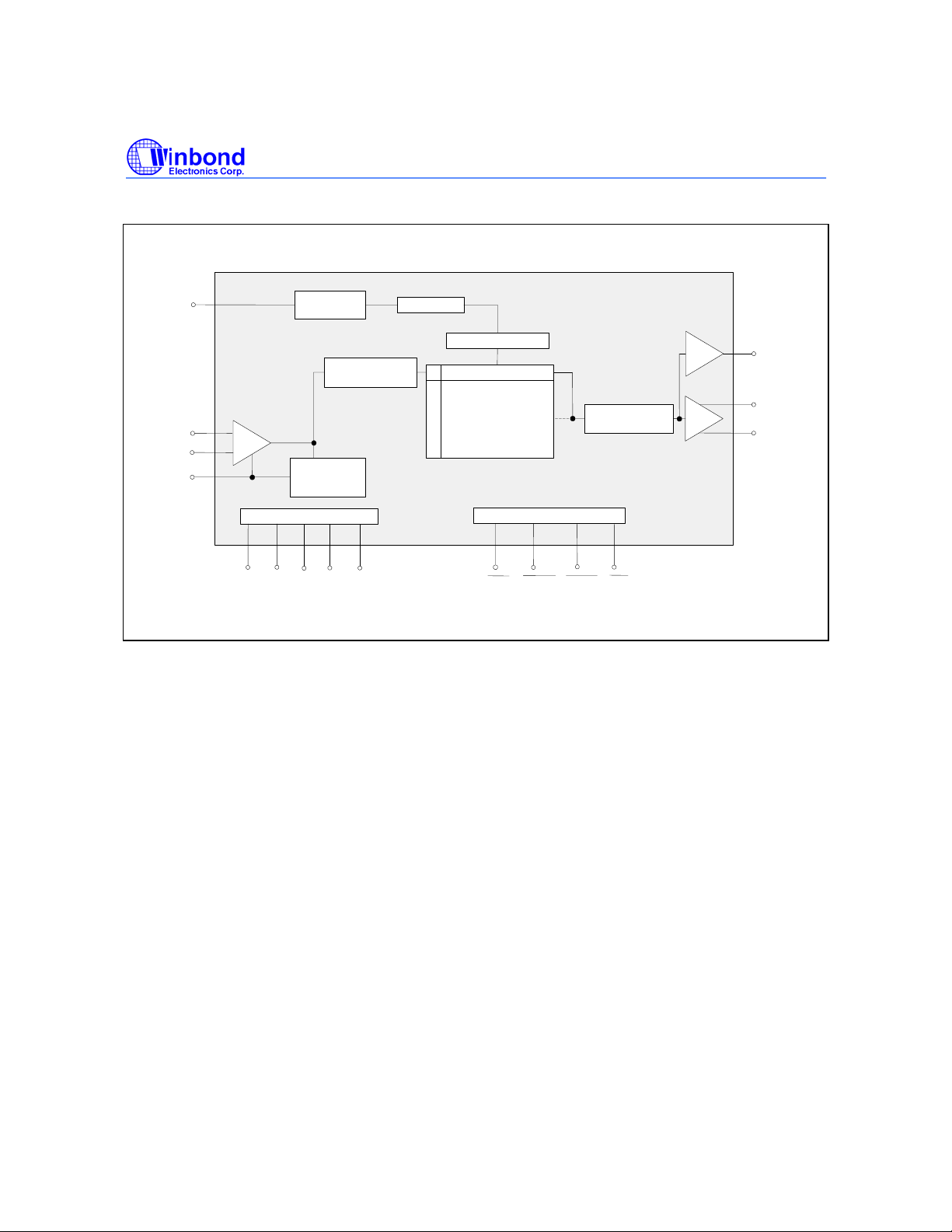
3. BLOCK DIAGRAM
ISD1600 SERIES
R
OSC
MIC+
MIC-
AGC
AGC
Amp
Power Conditioning
V
CCAVSSA
Internal
Clock
Antialiasing Filter
Auto mati c
Gain Control
(AGC)
V
V
SSD
SSAD
Acti ve
V
CCD
Timing
Sampling Clock
Analog Transceivers
Multilevel Storage
Decoders
Nonvolatile
Arra y
Device Control
PLAYEREC
Acti ve
Smoothing Filter
LEDPLAYL
Amp
Amp
AUD
SP+
SP-
Publication Release Date: November 4, 2004
- 3 - Revision 1
Page 4

ISD1600 SERIES
4. TABLE OF CONTENTS
1. GENERAL DESCRIPTION.................................................................................................................. 2
2. FEATURES ......................................................................................................................................... 2
3. BLOCK DIAGRAM .............................................................................................................................. 3
4. TABLE OF CONTENTS ...................................................................................................................... 4
5. PIN CONFIGURATION ....................................................................................................................... 5
6. PIN DESCRIPTION............................................................................................................................. 6
7. FUNCTIONAL DESCRIPTION............................................................................................................ 8
7.1. Detailed Description.................................................................................................................. 8
8. TIMING DIAGRAMS.......................................................................................................................... 10
9. ABSOLUTE MAXIMUM RATINGS
[1]
................................................................................................ 12
9.1 Operating Conditions ............................................................................................................... 13
10. ELECTRICAL CHARACTERISTICS ............................................................................................... 14
10.1. DC Parameters...................................................................................................................... 14
10.2. AC Parameters...................................................................................................................... 15
11. TYPICAL APPLICATION CIRCUIT.................................................................................................16
12. PACKAGE DRAWING AND DIMENSIONS .................................................................................... 17
12.1. 16-Lead 150mil Small Outline IC (SOIC) Package.......................................................... 17
12.2. 16-Lead 300mil Plastic Dual Inline Package (PDIP) ....................................................... 18
12.3. Die Physical Layout .............................................................................................................. 19
13. ORDERING INFORMATION........................................................................................................... 20
14. VERSION HISTORY ....................................................................................................................... 21
- 4 -
Page 5
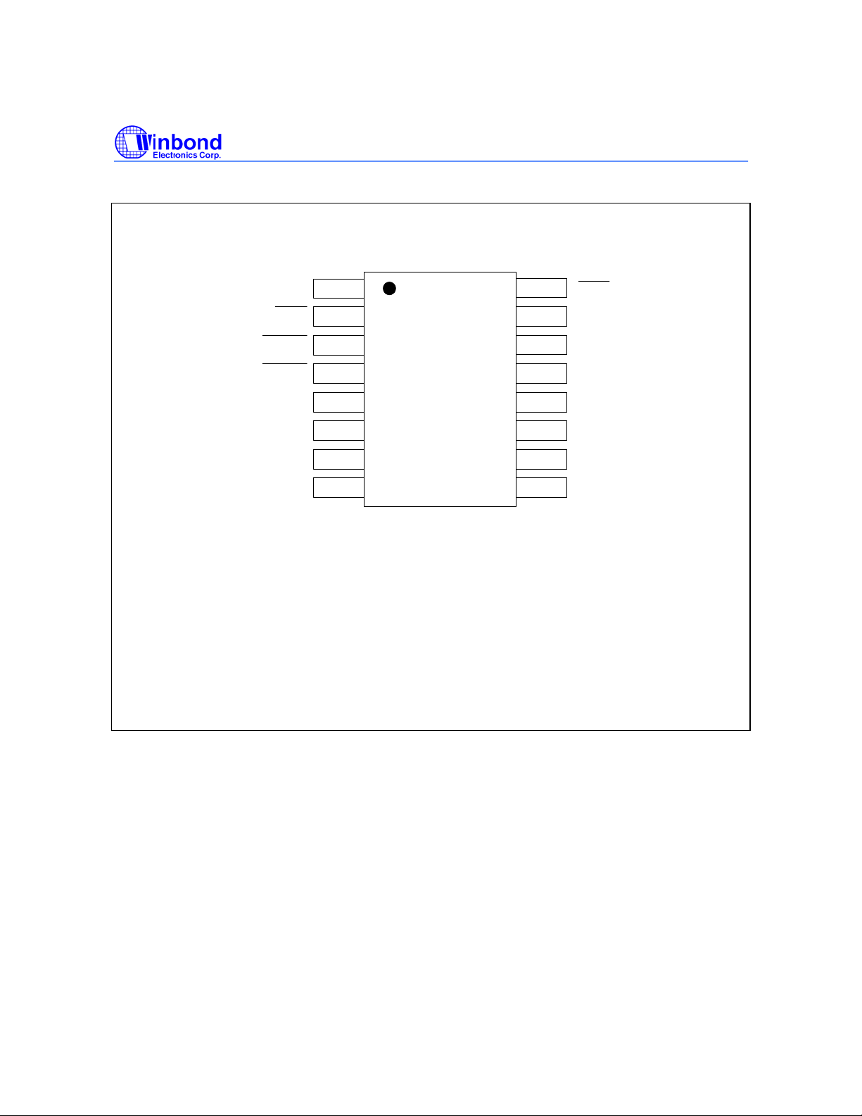
5. PIN CONFIGURATION
ISD1600 SERIES
V
SSD
REC
PLAYE
PLAYL
V
SSA
MIC+
MIC-
SP-
1
2
3
4
5
6
7
I1600
16
15
14
13
12
11
10
98
LED
V
CCD
R
OSC
AUD
AGC
Sp+
V
CCA
V
SSAD
SOIC / PDIP
Publication Release Date: November 4, 2004
- 5 - Revision 1
Page 6
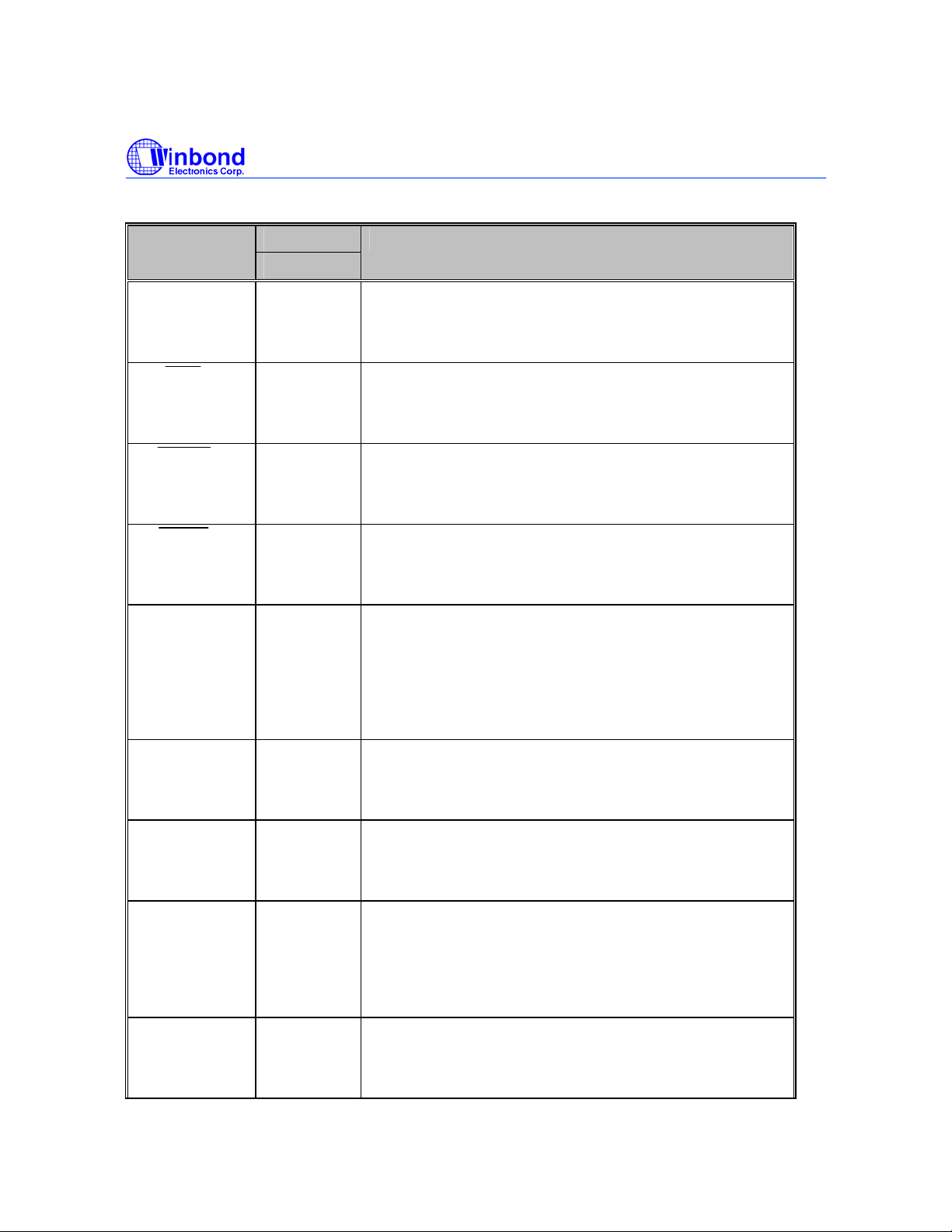
6. PIN DESCRIPTION
ISD1600 SERIES
SOIC / PDIP PIN NAME
PIN NO.
V
, V
SSD
V
SSAD
REC
PLAYE
PLAYL
,
SSA
[1]
2
[1]
3
[1]
4
1, 5, 9
MIC+ 6
FUNCTIONS
Ground: V
is the ground for digital circuits. V
SSD
ground for analog circuits, whereas V
is the ground for
SSAD
is the
SSA
PWM speaker driver. They should be separate ground paths
connecting to ground of power supply to minimize noises.
Record: The device starts recording whenever REC transits
from HIGH to LOW and stays at LOW. Recording stops
when the signal returns to HIGH. This pin has an internal
pull-up device
[2]
.
Edge-trigger Playback: A playback operation starts when
this input detects a LOW going signal exceeding the
specified debounced time. This pin has an internal pull-up
[2]
device
.
Level-trigger Playback: A playback operation begins when
this input detects a LOW going signal and remains at LOW.
Playback stops when the signal returns to HIGH. This pin
has an internal pull-up device
[2]
.
Microphone Positive Input: The input transfers the signals
to the preamplifier. The internal Automatic Gain Control
(AGC) circuit controls the gain of the preamplifier. An
external microphone should be AC coupled to this pin via a
series capacitor. The capacitor value, together with an
internal 10 K resistance on this pin, determines the lowfrequency cutoff for the ISD1600 passband.
MIC- 7
SP- 8
V
, V
CCA
10, 15
CCD
SP+ 11
Microphone Negative Input: This is the inverting input to
the microphone preamplifier. It provides input noisecancellation, or common-mode rejection, when the
microphone is connected differentially to the device.
Speaker Negative : The SP-, Class D PWM output, provide
a differential output with SP+ pin to drive 8 speaker or
buzzer. During power down or recording, this pin is tristated.
Supply Voltages: Internal analog and digital circuits use
separate power busses to minimize noises inside the chip.
These power busses are brought out to separate pads and
should be tied together as close to the power supply as
possible. It is important that the power supplies are
decoupled as close as possible to the device.
Speaker Positive : The SP+, Class D PWM output, provide
a differential output with SP- pin to drive an 8 speaker or
buzzer directly. During power down or recording, this pin is
tri-stated.
- 6 -
Page 7
ISD1600 SERIES
Note:
SOIC / PDIP PIN NAME
FUNCTIONS
PIN NO.
AGC 12
Automatic Gain Control: The AGC dynamically adjusts the
gain of the preamplifier to compensate the wide range of
microphone input levels. The AGC allows the full range of
signal to be recorded with minimal distortion. Nominal
values of 4.7 µF give satisfactory results in most cases.
Connecting this pin to ground provides maximum gain to the
preamplifier circuitry. Conversely, connecting this pin to
power supply provides minimum gain to the preamplifier
circuitry.
AUD 13
AUD: The AUD provides a single-ended current output to
drive an external amplifier. During standby or recording, this
pin is tri-stated.
R
14
OSC
Oscillator Resistor: This enables the user to vary the
record and/or playback duration of the device. A resistor
connected between the R
pin and VSS determines the
OSC
sample frequency for the ISD1600 device. Please refer to
the Duration Section in Section 7.1.
16 : This output is LOW during a record cycle and blinks
LED
LED
during playback cycle. It can be used to drive an LED to
indicate either a record or playback cycle is in progress.
[1]
The REC and Play signal are internally debounced on the falling edge to prevent a false re-triggering
from a push-button switch.
[2]
The internal pull-up resistors are 600kΩ (typical).
Publication Release Date: November 4, 2004
- 7 - Revision 1
Page 8
ISD1600 SERIES
7. FUNCTIONAL DESCRIPTION
7.1. DETAILED DESCRIPTION
Audio Quality
®
Winbond’s patented ChipCorder
solution on a single chip. The input audio signals are stored directly into the non-volatile memory and
are reproduced in its natural form without any compression artifacts caused by the digital speech
solutions. A complete sample is stored in a single cell, minimizing the memory needed to store a
single message.
Duration
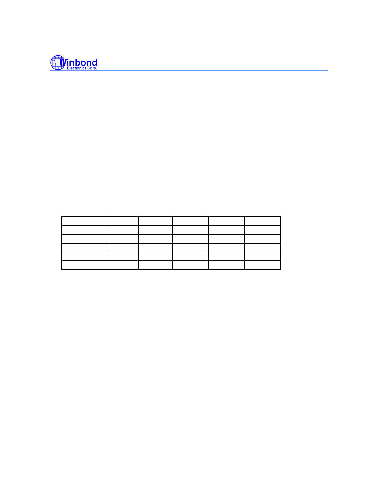
The ISD1600 series offer single-chip solution with record/playback duration from 6.6 seconds to 40
seconds. Sampling rate and duration are determined by an external resistor connected to the Rosc
pin.
Sample Rate
12 KHz
8 KHz
6.4 KHz
5.3 KHz
4 KHz
Rosc
60 kΩ
80 kΩ
100 kΩ
120 kΩ
160 kΩ
MLS technology provides natural high quality record and playback
ISD1610 ISD1612 ISD1616 ISD1620
6.6 secs 8 secs 10.6 secs 13.3 secs
10 secs 12 secs 16 secs 20 secs
12.5 secs 15 secs 20 secs 25 secs
15 secs 18 secs 24 secs 30 secs
20 secs 24 secs 32 secs 40 secs
Flash Storage
The ISD1600 product utilizes the on-chip Flash memory providing zero-power message storage. The
message is retained for up to 100 years without power. In addition, the device can be re-recorded
typically over 10,000 times.
Basic Operation
®
The ISD1600 ChipCorder
device is controlled by either the REC pin, or one of the two playback
modes, PLAYE and PLAYL. The ISD1600 parts are configured for design simplicity in a singlemessage application. Device operation is explained in Section 7.2.
Automatic Power-Down Mode
At the end of a playback or record cycle, the
ISD1600 device automatically enters into a low-power
standby mode, consuming typically 0.5µA, provided that PLAY and REC pins are HIGH (see DC
parameters, Section 10). During a playback cycle, the device powers down automatically at the end of
the message. During a record cycle, the device powers down immediately after REC is released to
HIGH.
- 8 -
Page 9

ISD1600 SERIES
7.2. Functional Description Example
The following example operating sequences demonstrate the functionality of the ISD1600 series.
1. Record a message
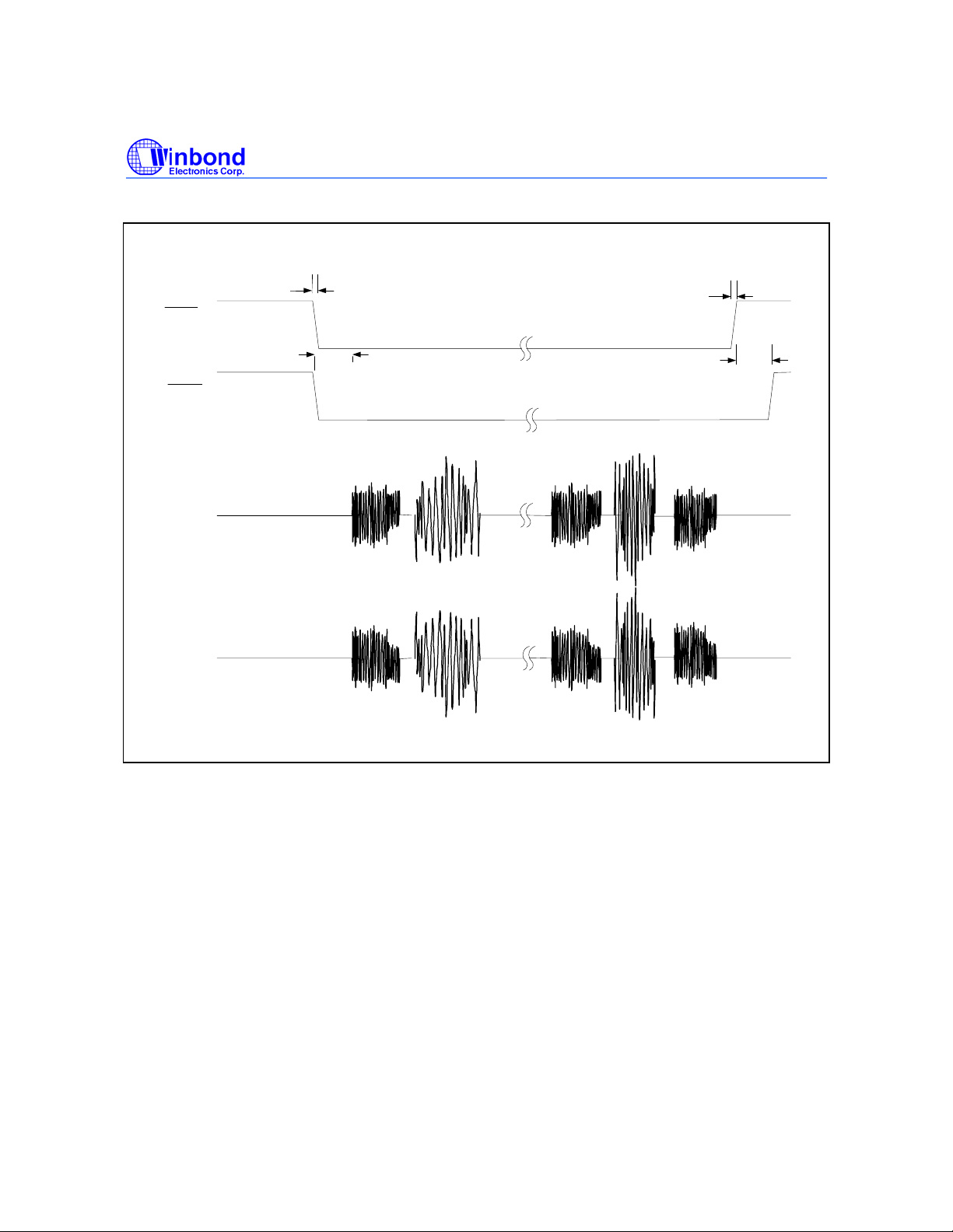
The device starts recording from the beginning of the memory when REC transits from HIGH to LOW
and stays at LOW. A record cycle is completed when REC is pulled to HIGH or entire memory is filled
up. Then an End-of-Message (EOM) marker is written at the end of message, enabling a subsequent
playback cycle to terminate appropriately. Hence, the device automatically enters into standby mode.
REC takes precedence over any playback operations. If REC is pulled LOW during a playback cycle,
the playback immediately halts and recording starts from the beginning of the memory.
The REC pin has an internal pull-up device
standby current consumption.
2. Edge-trigger playback
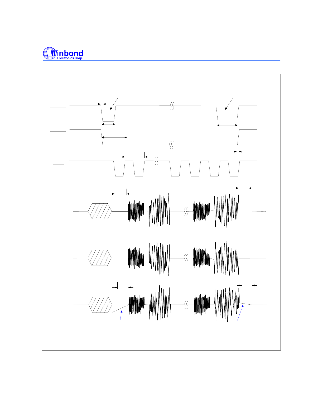
A playback operation starts from the beginning of the memory when PLAYE detects a LOW going
signal exceeding the specified debounced time. Playback continues until an EOM marker is
encountered. Upon completion of a playback cycle, the device automatically powers down and enters
into standby mode.
During playback, a subsequent LOW going signal will terminate the current playback operation.
This pin has an internal pull-up device
standby current consumption.
3. Level- trigger playback
When PLAYL switches from HIGH to LOW and stays at LOW, a playback starts from the beginning of
the memory until either an EOM marker is reached, then it automatically powers down.
If PLAYL is pulled HIGH any time during playback, the playback operation stops immediately and the
device enters into the power-down mode.
4. LED operation
The output pin provides an active-LOW signal during recording, which is used to turn on an LED
LED
as a “record-in-progress” indicator. However, during playback, the LED blinks a few times per second
to indicate a “playback-in-progress” operation. It returns to a HIGH state when operation stops.
5. R
operation
OSC
The duration of the device can be varied by changing the value of R
the flexibility to choose different sampling frequency, up to 12 KHz, depending upon the needs.
This feature allows frequency shifting where a recorded audio can be played back faster or slower
than normal for special sound effects.
Another feature is a “Pause” function that can be activated by taking the R
playback momentarily, and to resume when the resistor is switched back to ground.
[2]
. Holding this pin LOW after recording cycle will increase
[2]
. Holding this pin LOW after playback operation will increase
. This means the designer has
OSC
resistor to V
OSC
to stop
CC
Publication Release Date: November 4, 2004
- 9 - Revision 1
Page 10
8. TIMING DIAGRAMS
ISD1600 SERIES
Rec
LED
Mic+
Mic-
Tf
Tr
TRS
TDb1
FIGURE 1: RECORD OPERATION
- 10 -
Page 11
ISD1600 SERIES
PlayE
PlayL
LED
Sp+
Odd # pulses starts playback
Tf
TDb2
TDb1
Tcyc
TRU
Even # pulses stops playback
TDb1
Tr
TPS1 or TPS2
Sp-
TPS1 or TPS2
Aud
TRU
Ramps up gradually to analog ground
to eliminate the "pop" at the beginning
Slowly returns to analog ground
to eliminate the "pop" at the end
FIGURE 2: PLAYBACK OPERATION
Publication Release Date: November 4, 2004
- 11 - Revision 1
Page 12
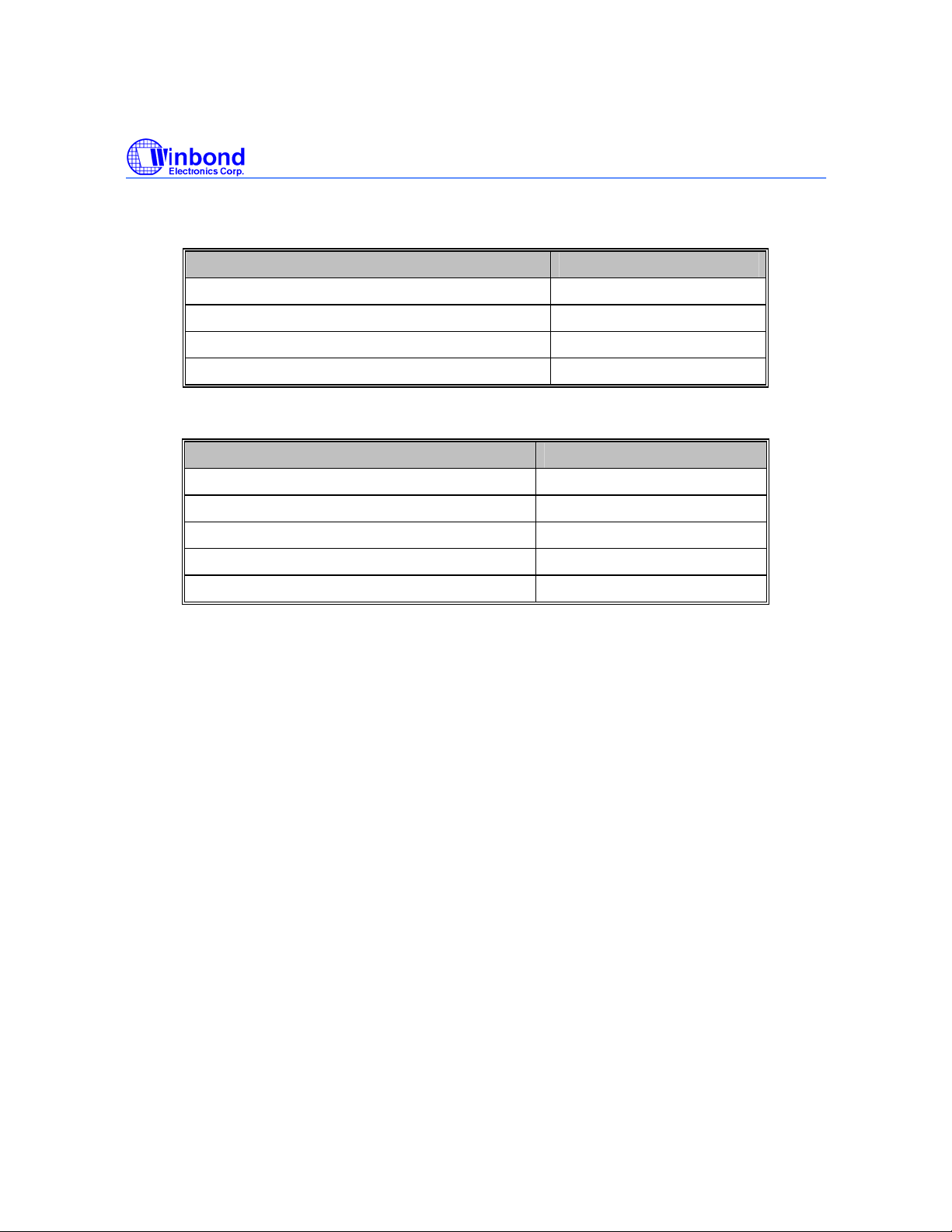
9. ABSOLUTE MAXIMUM RATINGS
ABSOLUTE MAXIMUM RATINGS (DIE)
CONDITIONS VALUES
Junction temperature 150°C
Storage temperature range -65°C to +150°C
Voltage applied to any pins (VSS –0.3V) to (VDD +0.3V)
Power supply voltage to ground potential -0.3V to +7.0V
ABSOLUTE MAXIMUM RATINGS (PACKAGED PARTS)
CONDITIONS VALUES
Junction temperature 150°C
Storage temperature range -65°C to +150°C
Voltage applied to any pins (VSS –0.3V) to (VDD +0.3V)
Lead temperature (Soldering – 10 sec) 300°C
ISD1600 SERIES
[1]
Power supply voltage to ground potential -0.3V to +7.0V
[1]
Stresses above those listed may cause permanent damage to the device. Exposure to the
absolute maximum ratings may affect device reliability and performance. Functional operation is
not implied at these conditions.
- 12 -
Page 13
ISD1600 SERIES
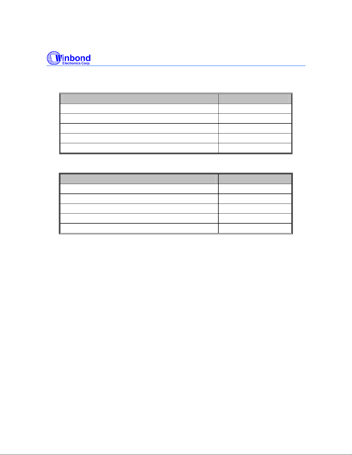
9.1 OPERATING CONDITIONS
OPERATING CONDITIONS (DIE)
CONDITIONS VALUES
Operating temperature range 0°C to +50°C
Supply voltage (VDD)
Ground voltage (VSS)
Input voltage (VDD)
Voltage applied to any pins (VSS –0.3V) to (VDD +0.3V)
Operating temperature range (Case temperature) -40°C to +85°C
Supply voltage (VDD)
Ground voltage (VSS)
Input voltage (VDD)
[1]
+2.4V to +5.5V
[2]
0V
[1]
0V to 5.5V
OPERATING CONDITIONS (PACKAGED PARTS)
CONDITIONS VALUES
[1]
+2.4V to +5.5V
[2]
0V
[1]
0V to 5.5V
Voltage applied to any pins (VSS –0.3V) to (VDD +0.3V)
[1]
VDD = V
[2]
VSS = V
CCA
SSA
= V
= V
CCD
SSD
= V
SSAD
Publication Release Date: November 4, 2004
- 13 - Revision 1
Page 14
10. ELECTRICAL CHARACTERISTICS
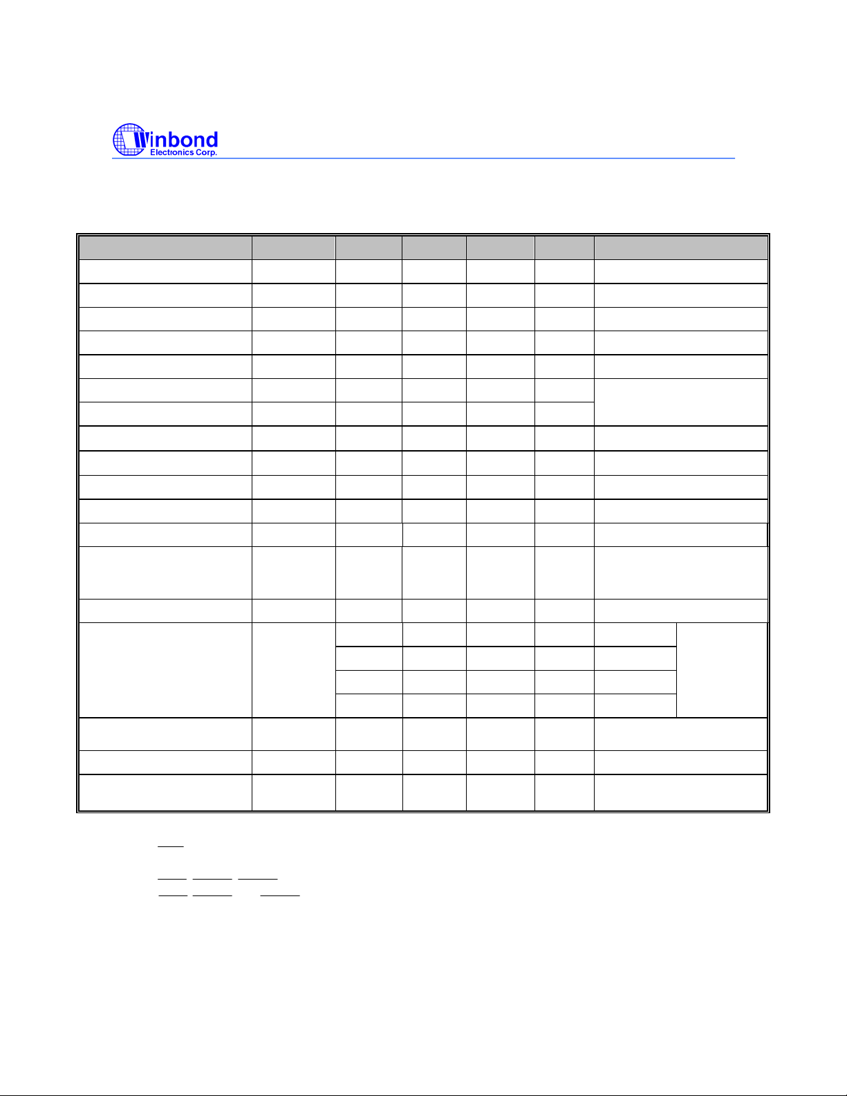
10.1. DC PARAMETERS
ISD1600 SERIES
PARAMETER SYMBOL MIN TYP
[1]
MAX UNITS CONDITIONS
Supply Voltage VDD 2.4 5.5 V
Input Low Voltage VIL V
-0.3 0.3xVDD V
SS
Input High Voltage VIH 0.7xVDD VDD V
Output Low Voltage VOL V
Output High Voltage VOH 0.7xVDD VDD V I
Record Current I
Playback Current I
DD_Record
DD_Playback
20 mA
20 mA
Standby Current ISB 0.5 1 µA
Input Leakage Current I
Input Current HIGH I
Preamp Input Resistance R
ILPD1
-3 -10 µA Force V
ILPD2
MIC+,RMIC-
20 K Across both pins
-0.3 0.3xVDD V I
SS
±1
µA Force V
= 4.0 mA
OL
= -1.6 mA
OH
V
= 5.5V, No load,
DD
Sampling freq = 12 kHz
V
= 5.5V, T=25°C
DD
[5]
DD
[5]
SS
MIC Input Voltage VIN 15 300 mV Peak-to-Peak
Gain from MIC to SP+/- A
6 40 dB VIN = 15 to 300mV,
MSP
AGC = 4.7µF,
V
= 2.4V to 5.5V
DD
Output Load Impedance R
Speaker Output Power Pout
Speaker Output Voltage Vout VDD V
8 Speaker Load
EXT
= 5.5V
V
670 mW
313 mW
117 mW
49 mW
DD
= 4.4V
V
DD
= 3V
V
DD
= 2.4V
V
DD
= 8 (Speaker),
R
EXT
70mH-160 (Buzzer)
AUD I
Total Harmonic Distortion THD 1 %
Notes:
[1]
Conditions: VCC = 4.5V, 8kHz sampling frequency and TA = 25°C, unless otherwise stated.
[2]
LED output during Record operation.
[3]
V
and V
CCA
[4]
REC, PLAYL, PLAYE must be at V
[5]
REC, PLAYL and PLAYE are forced to specified condition.
[6]
Balanced input signal applied between MIC and MIC REF as shown in the applications example. Single-
ended MIC or MIC REF recommended to be less than 100 mV peak to peak.
[7]
For industrial grade, the maximum limit is 10µA.
are connected together. V
CCD
-3.0 mA V
AUD
, V
CCD
SSAD
and V
SSA
.
are connected together.
SSD
=4.5V, R
DD
15mV p-p 1KHz sinewave,
Cmessage weighted
[2]
[2]
[3] [4] [7]
[6]
15mVp-p
1kHz freq
sinewave,
= 8;
R
EXT
= 100
EXT
- 14 -
Page 15
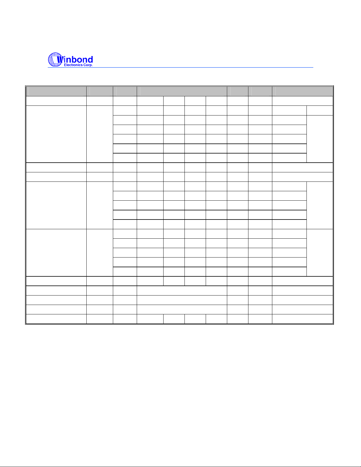
10.2. AC PARAMETERS
ISD1600 SERIES
CHARACTERISTIC SYMBOL MIN TYP
Sampling Frequency
Duration
[3]
Dur
[2]
FS 4 12 KHz Vcc=2.4V~5.5V
I1610 I1612 I1616 I1620
6.6 8 10.6 13.3 Sec SF=12kHz
10 12 16 20 Sec SF=8kHz
[1]
MAX UNITS CONDITIONS
Vcc=2.4
V~5.5V
12.5 15 20 25 Sec SF=6.4kHz
15 18 24 30 Sec SF=5.3kHz
20 24 32 40 Sec SF=4kHz
Rising time Tr 0 100 nsec
Falling Time Tf 0 100 nsec
Debounce Time
(Record & PlayL)
T
Db1
26.6 26.6 26.6 26.6 msec SF=12kHz
40 40 40 40 msec SF=8kHz
Vcc=2.4
V~5.5V
50 50 50 50 msec SF=6.4kHz
60.4 60.4 60.4 60.4 msec SF=5.3kHz
80 80 80 80 msec SF=4kHz
Debounce Time
(PlayE)
T
Db2
13.3 13.3 13.3 13.3 msec SF=12kHz
20 20 20 20 msec SF=8kHz
Vcc=2.4
V~5.5V
25 25 25 25 msec SF=6.4kHz
30.2 30.2 30.2 30.2 msec SF=5.3kHz
40 40 40 40 msec SF=4kHz
Signal Ramp Up Time TRU 100 msec Vcc=2.4V~5.5V
Record Stop Time TRS 2 Sample Clock Vcc=2.4V~5.5V
PlayL Stop Time T
PlayE Stop Time T
LED Cycle frequency T
T
PS1
2 X T
PS2
1 6 Hz Playback at any SF
Cyc
msec Vcc=2.4V~5.5V
Db1
msec Vcc=2.4V~5.5V
Db1
Notes:
[1]
Typical values : VCC = 4.5V, SF = 8 kHz and @ TA = 25°C, unless otherwise stated.
[2]
Sampling Frequency can vary as much as ±2.25 percent over the commercial temperature and voltage
ranges, and –6/+4 percent over the industrial temperature and voltage ranges.
[6]
Duration can vary as much as ±2.25 percent over the commercial temperature and voltage ranges, and –
6/+4 percent over the industrial temperature and voltage ranges.
Publication Release Date: November 4, 2004
- 15 - Revision 1
Page 16
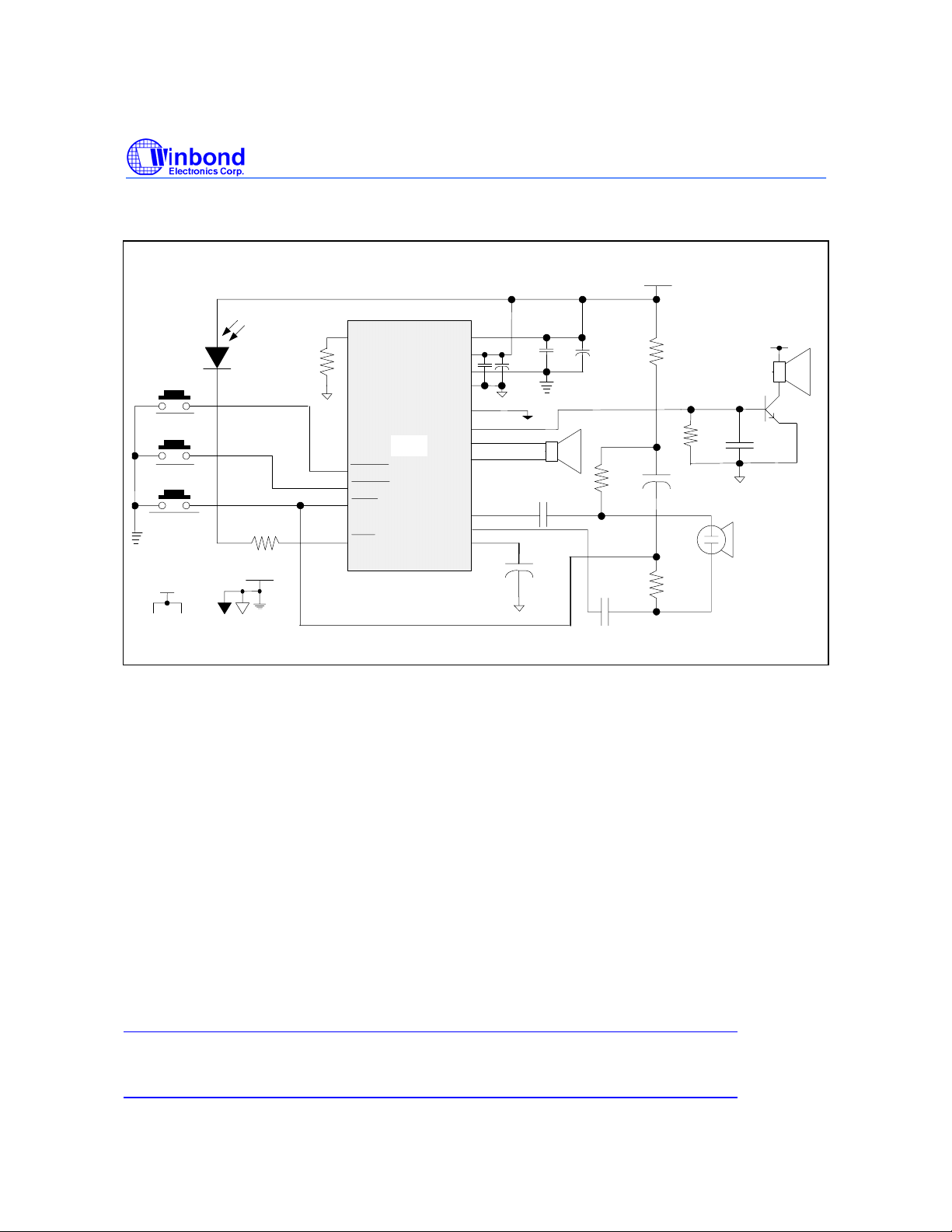
11. TYPICAL APPLICATION CIRCUIT
ISD1600 SERIES
V
CC
PLAYL
PLAYE
RECORD
V
CC
V
CCD
V
DI
LED
CCA
C3
µ
0.1 F
0.1 F
C9 *
µ
10 F
C4
0.1 F
µ
C6
4.7 F
µ
C8 *
µ
10 F
Speaker or
Buzzer
R3
4.7 K
C5
0.1 F
µ
1 K
R1
Ω
Q1
8050
R5
390
Ω
C1
µ
4.7 F
Ω
R4
4.7 K
ELECTRET
MICROPHONE
Ω
V
R
OSC
R2
Ω
80 K
I1800
1600
PLAYL
PLAYE
R6
1 K
Ω
V
SS
V
V
V
SSAD
SSD
SSA
REC
LED
V
V
V
V
SSAD
AUD
SP+
SP-
MIC+
MIC -
AGC
CCD
CCA
SSD
SSA
C2
µ
V
CC
C7
0.1 F
8
Speaker
µ
Ω
Schematic shows both speaker and AUD outputs
* C8 and C9 may be needed in order to optimize for the best voice quality, which is also depended upon the layout
of the PCB. Please refer to ChipCorder Applications section or consult Winbond for layout advice.
The above example represents a typical implementation of ISD1600 in most applications.
In addition, it is important to have a separate path for each ground (V
SSD
, V
SSA
& V
) back to the
SSAD
ground terminal of power source to minimize the noises. Please refer to the ChipCorder Applications
section in our website.
Good Audio Design Practices
Winbond products are very high-quality single-chip voice recording and playback systems. To ensure
the highest quality voice reproduction, it is important that good audio design practices on layout and
power supply decoupling be followed. See Application Information or below links for details.
Good Audio Design Practices
http://www.winbond-usa.com/products/isd_products/chipcorder/applicationinfo/apin11.pdf
Single-Chip Board Layout Diagrams
http://www.winbond-usa.com/products/isd_products/chipcorder/applicationinfo/apin12.pdf
- 16 -
Page 17
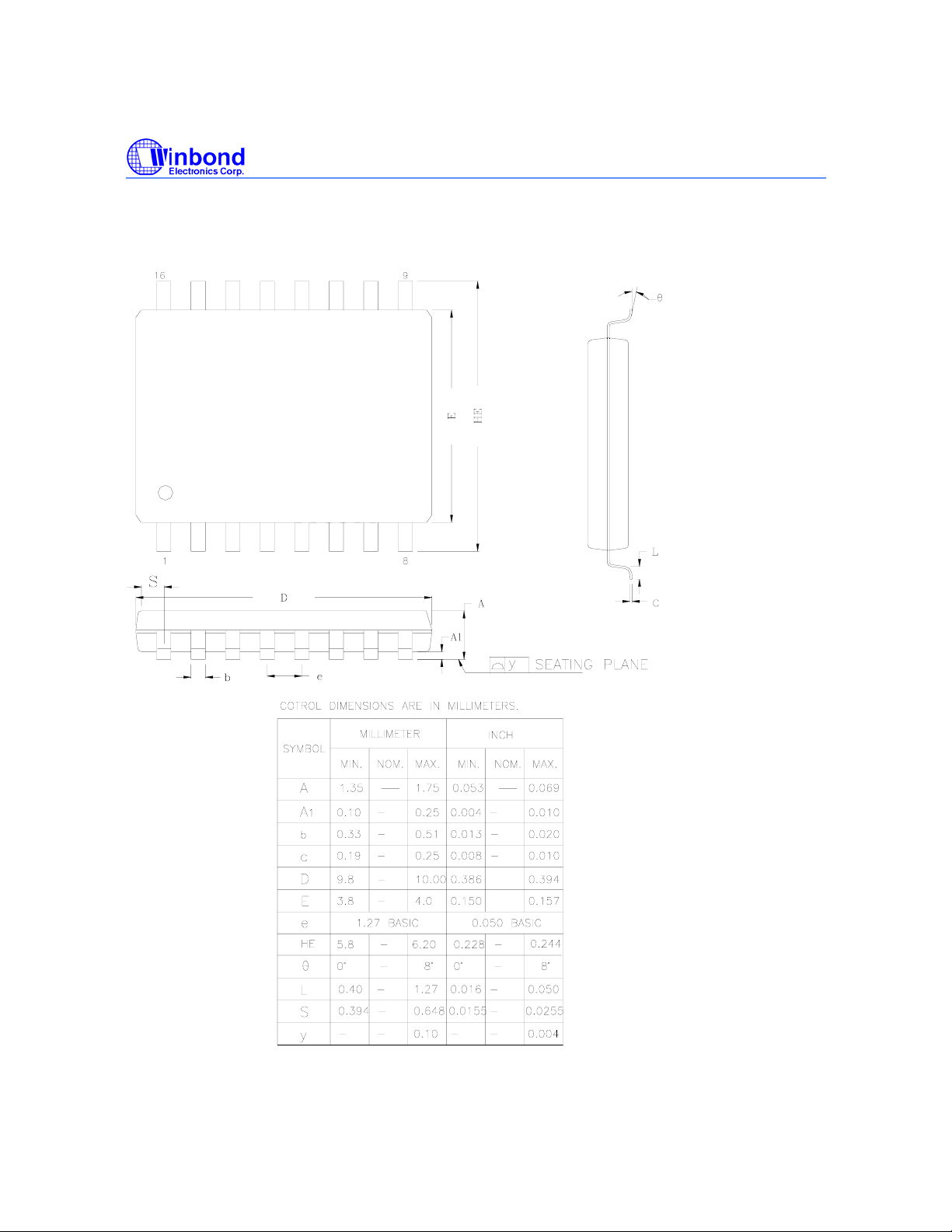
12. PACKAGE DRAWING AND DIMENSIONS
12.1. 16-LEAD 150MIL SMALL OUTLINE IC (SOIC) PACKAGE
ISD1600 SERIES
Publication Release Date: November 4, 2004
- 17 - Revision 1
Page 18
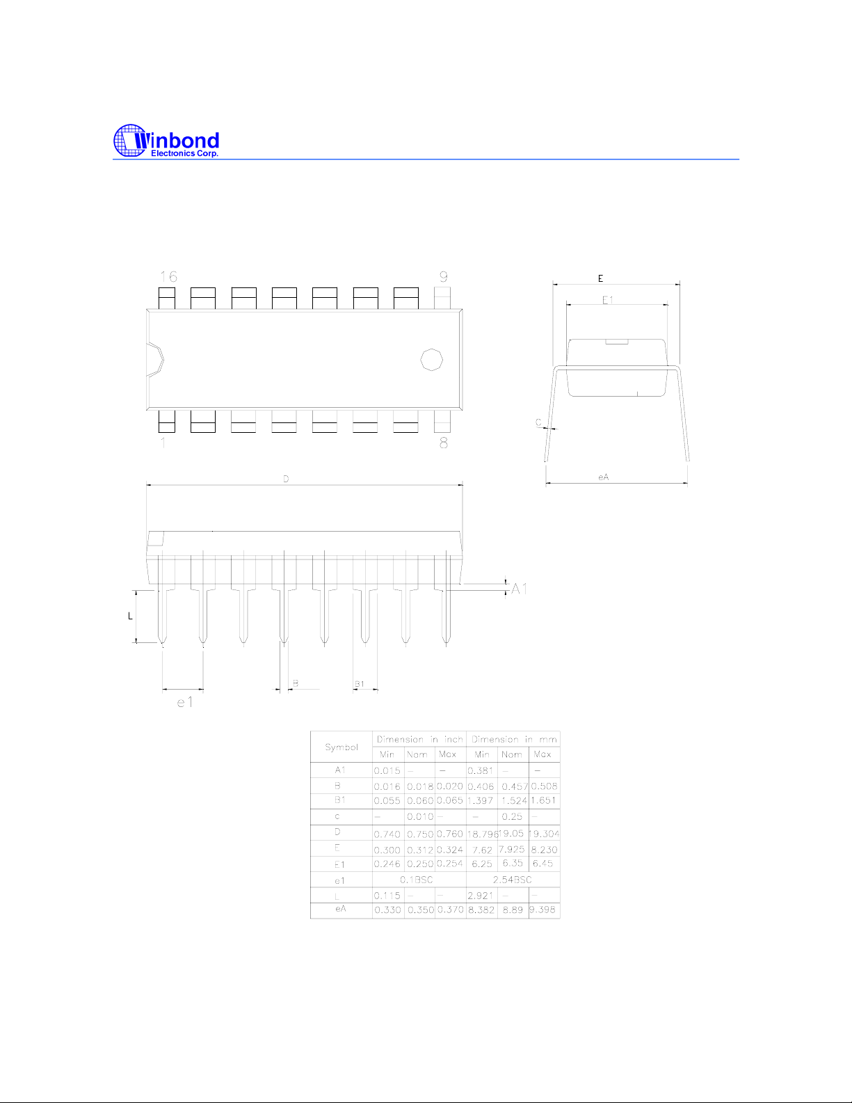
12.2. 16-Lead 300mil Plastic Dual Inline Package (PDIP)
ISD1600 SERIES
- 18 -
Page 19
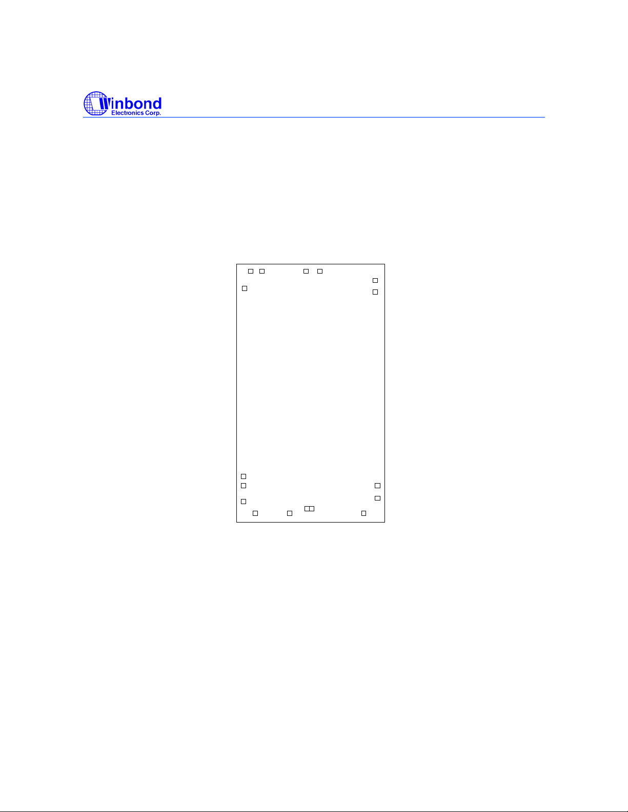
ISD1600 SERIES
12.3. DIE PHYSICAL LAYOUT
ISD1610 / 1612 / 1616 / 1620
REC
PLAYE
PLAYL
V
SSA
MIC+
MIC-
SP-
Notes:
[1]
The backside of die is internally connected to VSS. It MUST NOT be connected to any other potential or damage may occur.
SSAD
V
V
SSD
V
CCA
LED
CCA
V
SP+
V
CCD
R
OSC
AUD
AGC
Publication Release Date: November 4, 2004
- 19 - Revision 1
Page 20
ISD1600 SERIES
13. ORDERING INFORMATION
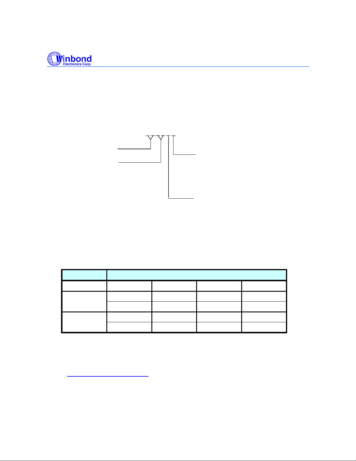
Product Number Descriptor Key
When ordering, please refer to the following part numbers that are supported in volume for this
product series. Consult the local Winbond Sales Representative or Distributor for availability
information.
I1600 Series
Duration:
I1610 : 6.6 – 20 secs
I1612 : 8 – 24 secs
I1616 : 10.6 – 30 secs
I1620 : 13.3 – 40 secs
I16xxxx
Temperature:
I = Industrial (-40°C to +85°C)
Blank = Commerical
• Die (0°C to +50°C)
• Package (0°C to +70°C)
Package Type:
X = Die
S = Small Outline Integrated Circuit
(SOIC) Package
P = Plastic Dual Inline Package (PDIP)
Die / Package Ordering Part Number
Die I1610X I1612X I1616X I1620X
I1610P I1612P I1616P I1620P PDIP
I1610PI I1612PI I1616PI I1620PI
I1610S I1612S I1616S I1620S SOIC
I1610SI I1612SI I1616SI I1620SI
For the latest product information, access Winbond’s worldwide website at
http://www.winbond-usa.com
- 20 -
Page 21

ISD1600 SERIES
14. VERSION HISTORY
VERSION DATE DESCRIPTION
0.1 July 2004
1 Nov. 2004
Initial draft
Revise Ground description
Revise application diagram
Revise die information
Publication Release Date: November 4, 2004
- 21 - Revision 1
Page 22

ISD1600 SERIES
f
f
r
r
A
A
The contents of this document are provided only as a guide for the applications of Winbond products. Winbond
makes no representation or warranties with respect to the accuracy or completeness of the contents of this
publication and reserves the right to discontinue or make changes to specifications and product descriptions at
any time without notice. No license, whether express or implied, to any intellectual property or other right o
Winbond or others is granted by this publication. Except as set forth in Winbond's Standard Terms and
Conditions of Sale, Winbond assumes no liability whatsoever and disclaims any express or implied warranty o
merchantability, fitness for a particular purpose or infringement of any Intellectual property.
Winbond products are not designed, intended, authorized or warranted for use as components in systems o
equipments intended for surgical implantation, atomic energy control instruments, airplane or spaceship
instruments, transportation instruments, traffic signal instruments, combustion control instruments, or for othe
applications intended to support or sustain life. Furthermore, Winbond products are not intended for applications
wherein failure of Winbond products could result or lead to a situation wherein personal injury, death or severe
property or environmental injury could occur.
pplication examples and alternative uses of any integrated circuit contained in this publication are for illustration
only and Winbond makes no representation or warranty that such applications shall be suitable for the use
specified.
The 100-year retention and 10K record cycle projections are based upon accelerated reliability tests, as published
in the Winbond Reliability Report, and are neither warranted nor guaranteed by Winbond. This product
incorporates SuperFlash
Information contained in this Winbond ChipCorder
products published by ISD® prior to August, 1998.
This datasheet and any future addendum to this data sheet is(are) the complete and controlling ISD
product specifications. In the event any inconsistencies exist between the information in this and other product
documentation, or in the event that other product documentation contains information in addition to the information
in this, the information contained herein supersedes and governs such other information in its entirety.
Copyright© 2003, Winbond Electronics Corporation. All rights reserved. ISD
trademarks of Winbond Electronics Corporation. SuperFlash
ll other trademarks are properties of their respective owners.
®
technology.
®
datasheet supersedes all data for the ISD® ChipCorder
®
ChipCorder
®
®
is the trademark of Silicon Storage Technology, Inc.
and ChipCorder® are registered
®
®
Headquarters Winbond Electronics Corporation America Winbond Electronics (Shanghai) Ltd.
No. 4, Creation Rd. III 2727 North First Street, San Jose, 27F, 299 Yan An W. Rd. Shanghai,
Science-Based Industrial Park, CA 95134, U.S.A. 200336 China
Hsinchu, Taiwan TEL: 1-408-9436666 TEL: 86-21-62365999
TEL: 886-3-5770066 FAX: 1-408-5441797 FAX: 86-21-62356998
FAX: 886-3-5665577 http://www.winbond-usa.com/
http://www.winbond.com.tw/
Taipei Office Winbond Electronics Corporation Japan Winbond Electronics (H.K.) Ltd.
9F, No. 480, Pueiguang Rd. 7F Daini-ueno BLDG. 3-7-18 Unit 9-15, 22F, Millennium City,
Neihu District Shinyokohama Kohokuku, No. 378 Kwun Tong Rd.,
Taipei, 114 Taiwan Yokohama, 222-0033 Kowloon, Hong Kong
TEL: 886-2-81777168 TEL: 81-45-4781881 TEL: 852-27513100
FAX: 886-2-87153579 FAX: 81-45-4781800 FAX: 852-27552064
Please note that all data and specifications are subject to change without notice.
All the trademarks of products and companies mentioned in this datasheet belong to their respective owners.
- 22 -
 Loading...