

Page 1
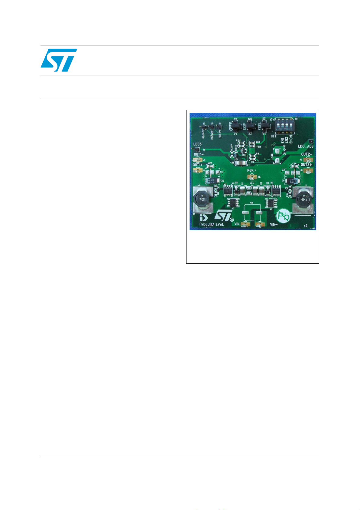
Demonstration board for the PM6680A dual synchronous
step-down controller with adjustable output voltages plus LDO
Features
■ Constant on-time control allows very fast load
transients
■ 6 V to 36 V input voltage range
■ 5 V auxiliary output voltage
■ Adjustable switching outputs
■ Lossless current sensing
■ Negative current limit
■ Soft-start internally fixed at 2.8 ms
■ Soft-end for output discharge
■ 200 kHz / 300 kHz, 300 kHz / 400 kHz, 400 kHz
/ 500 kHz (OUT1 / OUT2 selectable switching
frequency)
■ Selectable pulse skip and no-audible skip
modes at light loads
■ Independent power good signals
STEVAL-ISA053V2
Data Brief
STEVAL-ISA053V2
Description
The PM6680A is a dual step-down controller with
adjustable output voltages. This demonstration
board is designed to test the performance of the
PM6680A by employing a typical application
circuit which allows testing of all the PM6680A
device functions. The kit features two switching
sections, with (typically) 3.3 V and 1.8 V outputs,
from a 6 V to 36 V input voltage.
The typical operating switching frequency of the
two switching sections is 200 kHz / 300 kHz,
respectively. Each switching section delivers more
than 2.5 A of output current.
Moreover, an internal linear regulator can provide
5 V @ 100 mA peak current.
June 2008 Rev 1 1/4
For further information contact your local STMicroelectronics sales office.
www.st.com
4
Page 2
Circuit schematic STEVAL-ISA053V2
LDO_FB
BOOT2
BOOT1
BOOT2
BOOT1
FB1
FB1
LDO_FB
PGND
PGND
VIN
V5SW
OUT5V
OUT5V
SGND
V+
V+
VIN
SGND
SGND
V+
SGND
SGND
SGND
PGND
PGND
SGND
V+
V+
V+
SGND
SGND
SGND
PGND
PGND
VIN
OUT5V
V5SW
PGND
SGND
SGND
PGND
PGND
PGND
SGND
SGND
SGND
V+
SGND
SGND
SGND
SGND
SGND
LIKE 4-PIN JUMPER
A - S12 CLOSED
B - S14 CLOSED
C - S12.1 TO S14.2
M1
MOSFET-N-SO8
M1
MOSFET-N-SO8
C9
100n
C9
100n
C17
NM
C17
NM
J3
LDO5V+
J3
LDO5V+
C27
1uF
C27
1uF
J10
PGND
J10
PGND
500R
500R
3V3L1L1
3V3
C4
15u
C4
15u
R251K1K
R251K1K
D2
SMA
D2
SMA
R1
100K
R1
100K
R6
NM
R6
NM
J9
OUT2-
J9
OUT2-
C19
100n
C19
100n
C12
330uF
C12
330uF
C13
NM
C13
NM
C24
100n
C24
100n
M2
MOSFET-N-SO8
M2
MOSFET-N-SO8
C20
1uF
C20
1uF
J6
PGOOD1
J6
PGOOD1
R31
R31
C5
100n
C5
100n
CIN
NM
CIN
NM
C22
220nF
C22
220nF
R27
R27
R4
NM
R4
NM
C3
15u
C3
15u
R29
R29
C15
150pF
C15
150pF
C8
NM
C8
NM
R32
R32
R10
10R
R10
10R
15uC1C1
15u
PGOOD2J7J7
PGOOD2
R33
R33
CREF
100n
CREF
100n
L2
5V
L2
5V
S1
JP2SO
S1
JP2SO
S10
JP4I
S10
JP4I
C26
4u7
C26
4u7
R24
1K
R24
1K
R16
100K
R16
100K
C6
100n
C6
100n
R9
47R
R9
47R
J4
OUT1+
J4
OUT1+
JP3SO
JP3SO
R17
560K
R17
560K
C25
100n
C25
100n
15uC2C2
15u
C16
100pF
C16
100pF
R14
100K
R14
100K
C10
100n
C10
100n
C21
4u7
C21
4u7
RLD5V
100K
RLD5V
100K
D3
SMA
D3
SMA
R28
R28
R30
R30
C14
NM
C14
NM
D1
BAT54A/SOT
D1
BAT54A/SOT
R8
500R
R8
500R
C11
330uF
C11
330uF
-VINJ2J2
-VIN
R11
10R
R11
10R
M4
MOSFET-N-SO8
M4
MOSFET-N-SO8
R20
0R
R20
0R
S4
JP2SO
S4
JP2SO
J8
OUT1-
J8
OUT1-
R3
NM
R3
NM
S3
JP4I
S3
JP4I
R22
0R
R22
0R
S1
JP2SO
S1
JP2SO
R26
3R9
R26
3R9
R18
560K
R18
560K
S9
JP3SO
S9
JP3SO
C18
NM
C18
NM
M3
MOSFET-N-SO8
M3
MOSFET-N-SO8
J11
EXT5V
J11
EXT5V
C7
NM
C7
NM
+VINJ5J5
+VIN
S5
JP2SO
S5
JP2SO
LDO_ADJ
LDO_ADJ
C28
4u7
C28
4u7
JP3SOS8S8
JP3SO
R23
0R
R23
0R
R19
560K
R19
560K
U1
PM6681_VFQFPN32
U1
PM6681_VFQFPN32
BOOT1
23
HGATE1
22
PHASE1
21
CSENSE1
20
V5SW
17
OUT1
29
COMP1
30
LDO_FB
16
LGATE1
15
PGOOD1
26
PGOOD2
27
SHDN
SKI
FSE
LDO
BOOT2
HGATE2
10
PHASE2
11
CSENSE2
12
PGND
14
SGND
OUT2
COMP2
FB2
FB1
28
LDO
LGATE2
13
C23
10pF
C23
10pF
R5
NM
R5
NM
R15
100K
R15
100K
R2
0R
R2
0R
S2
SWDIP-4
S2
SWDIP-4
J1
OUT2+
J1
OUT2+
R1
100K
R1
100K
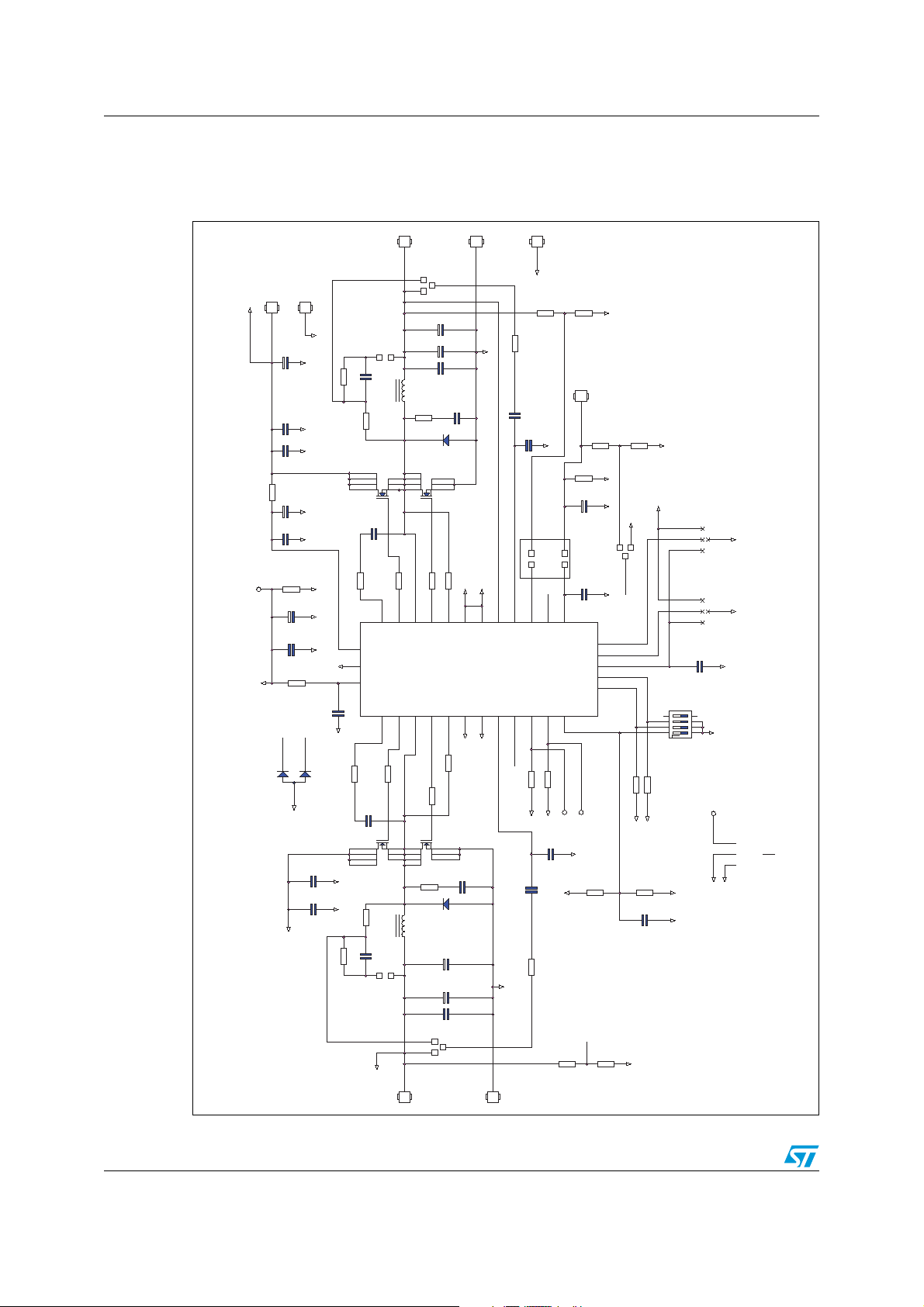
1 Circuit schematic
Figure 1. Schematic diagram
J10
OUT2+
OUT2+
J1
J1
1
J2J2-VIN
-VIN
J5J5+VIN
+VIN
VIN
2/4
LDO5V+
LDO5V+
J3
J3
R26
R26
V+
D1
D1
1
1
PGND
CIN
CIN
NM
NM
+
+
PGND
C2C215u
15u
PGND
C1C115u
15u
PGND
3R9
3R9
4u7
4u7
C26
C26
+
+
SGND
100n
100n
C19
C19
SGND
RLD5V
RLD5V
100K
100K
SGND
4u7
4u7
C21
C21
+
+
SGND
C20
1uF
C20
1uF
SGND
47R
47R
R9
R9
C22
C22
BOOT2
BOOT1
2
1
BAT54A/SOT
BAT54A/SOT
3
V+
15u
15u
C4
C4
15u
15u
C3
C3
VIN
S4
S4
JP2SO
JP2SO
1 2
C13
C13
R3
R3
8
7
6
51
BOOT2
10R
10R
U1
U1
VIN
5
10R
10R
C6
C6
51
6
7
8
R4
R4
C14
C14
NM
NM
NM
NM
C5
C5
LDO
VCC
100n
100n
NM
NM
NM
NM
OUT5V
M1
M1
MOSFET-N-SO8
MOSFET-N-SO8
4
100n
100n
9
BOOT2
BOOT1
23
R22
R22
4
M2
M2
MOSFET-N-SO8
MOSFET-N-SO8
S5
S5
JP2SO
JP2SO
2
L1L13V3
1
3
2
R20
R20
10
HGATE2
HGATE1
22
0R
0R
2
3
12
L2
L2
1 2
1
J4
J4
3V3
8
7
6
51
0R
0R
11
21
M4
M4
51
6
7
8
R5
R5
NM
NM
R11
R11
19
18
V+
31
220nF
220nF
SGND
R10
R10
BOOT1
PGND
PGND
R6
R6
NM
NM
S8S8JP3SO
JP3SO
3
1
560K
560K
R18
R18
M3
M3
MOSFET-N-SO8
MOSFET-N-SO8
4
1 0R
1 0R
R2
R2
13
PHASE2
PHASE1
15
R23
R23
4
MOSFET-N-SO8
MOSFET-N-SO8
5V
5V
S9
S9
3
1
OUT1+
OUT1+
2
C8
C8
NM
NM
+
+
C7
C7
NM
NM
+
+
C24
100n
C24
100n
D3
D3
SMA
SMA
12
3
2
R7 500R
R7 500R
12
LGATE2
LGATE1
20
R8
R8
0R
0R
2
3
R19
R19
560K
560K
12
D2
D2
SMA
SMA
C12
C12
330uF
330uF
+
+
C11
C11
330uF
330uF
+
+
C25
C25
JP3SO
JP3SO
C9
C9
CSENSE2
CSENSE1
100n
100n
2
J9
J9
1
100n
100n
PGND
14
PGND
V5SW
17
V5SW
500R
500R
100n
100n
C10
C10
J10
PGND
OUT2-
OUT2-
R25
R25
PGND
C15
C15
SGND
1
8
OUT2
SGND
COMP1
OUT1
29
30
OUT5V
1
J8
J8
PGND
1
PGND
R30
?
R30
?
?
?
R29
R29
SGND
LDO_ADJ
LDO_ADJ
NM
NM
SGND
A - S12 CLOSED
LIKE 4-PIN JUMPER
B - S14 CLOSED
FB1
28
FB1
PGOOD2
27
3 100K
3 100K
R1
R1
V+
C18
C18
100pF
100pF
1K
1K
+
+
C - S12.1 TO S14.2
12
3 JP2SO
3 JP2SO
S1
S1
7
LDO
SHDN
5
PGOOD1
PGOOD1
J7J7PGOOD2
J6
J6
NM
NM
VIN
R28
R28
?
?
1
R32
R32
?
?
R31
R31
?
?
SGND
R33
R33
?
?
SGND
4u7
4u7
C28
C28
SGND
C27
C27
1uF
1uF
SGND
FSE
L
3
SKI
P
24
VREF
32
EN1
25
EN2
4
PGOOD2
SGND
560K
560K
R17
R17
FB1
R27
R27
SGND
1
3
S1S1JP3SO
S1S1JP3SO
2
LDO_FB
PM6681_VFQFPN32
PM6681_VFQFPN32
R15
R15
100K
100K
V+V+V+
?
?
SGND
V+
JP4I
JP4I
S3
S3
4
31
2
JP4I
JP4I
S10
S10
4
31
2
SGND
100n
100n
CREF
CREF
4
5
3
6
2
7
1
8
S2
S2
R14
R14
100K
100K
R16
R16
100K
100K
C23
10pF
C23
10pF
SWDIP-4
SWDIP-4
SGND
SGND
SGND
J11
J11
EXT5V
EXT5V
V5SW
OUT5V
150pF
150pF
C17
C17
1
2 JP2SO
2 JP2SO
S1
S1
2
2
6
FB2
COMP2
LDO_FB
PGOOD1
26
16
LDO_FB
2 100K
2 100K
R1
R1
V+
C16
C16
R24
R24
PGND
OUT1-
OUT1-
Page 3
STEVAL-ISA053V2 Revision history
2 Revision history
Table 1. Document revision history
Date Revision Changes
06-June-2008 1 Initial release.
3/4
Page 4

STEVAL-ISA053V2
y
Please Read Carefully:
Information in this document is provided solely in connection with ST products. STMicroelectronics NV and its subsidiaries (“ST”) reserve the
right to make changes, corrections, modifications or improvements, to this document, and the products and services described herein at any
time, without notice.
All ST products are sold pursuant to ST’s terms and conditions of sale.
Purchasers are solely responsible for the choice, selection and use of the ST products and services described herein, and ST assumes no
liability whatsoever relating to the choice, selection or use of the ST products and services described herein.
No license, express or implied, by estoppel or otherwise, to any intellectual property rights is granted under this document. If any part of this
document refers to any third party products or services it shall not be deemed a license grant by ST for the use of such third party products
or services, or any intellectual property contained therein or considered as a warranty covering the use in any manner whatsoever of such
third party products or services or any intellectual property contained therein.
UNLESS OTHERWISE SET FORTH IN ST’S TERMS AND CONDITIONS OF SALE ST DISCLAIMS ANY EXPRESS OR IMPLIED
WARRANTY WITH RESPECT TO THE USE AND/OR SALE OF ST PRODUCTS INCLUDING WITHOUT LIMITATION IMPLIED
WARRANTIES OF MERCHANTABILITY, FITNESS FOR A PARTICULAR PURPOSE (AND THEIR EQUIVALENTS UNDER THE LAWS
OF ANY JURISDICTION), OR INFRINGEMENT OF ANY PATENT, COPYRIGHT OR OTHER INTELLECTUAL PROPERTY RIGHT.
UNLESS EXPRESSLY APPROVED IN WRITING BY AN AUTHORIZED ST REPRESENTATIVE, ST PRODUCTS ARE NOT
RECOMMENDED, AUTHORIZED OR WARRANTED FOR USE IN MILITARY, AIR CRAFT, SPACE, LIFE SAVING, OR LIFE SUSTAINING
APPLICATIONS, NOR IN PRODUCTS OR SYSTEMS WHERE FAILURE OR MALFUNCTION MAY RESULT IN PERSONAL INJURY,
DEATH, OR SEVERE PROPERTY OR ENVIRONMENTAL DAMAGE. ST PRODUCTS WHICH ARE NOT SPECIFIED AS "AUTOMOTIVE
GRADE" MAY ONLY BE USED IN AUTOMOTIVE APPLICATIONS AT USER’S OWN RISK.
Resale of ST products with provisions different from the statements and/or technical features set forth in this document shall immediately void
any warranty granted by ST for the ST product or service described herein and shall not create or extend in any manner whatsoever, an
liability of ST.
ST and the ST logo are trademarks or registered trademarks of ST in various countries.
Information in this document supersedes and replaces all information previously supplied.
The ST logo is a registered trademark of STMicroelectronics. All other names are the property of their respective owners.
© 2008 STMicroelectronics - All rights reserved
STMicroelectronics group of companies
Australia - Belgium - Brazil - Canada - China - Czech Republic - Finland - France - Germany - Hong Kong - India - Israel - Italy - Japan -
Malaysia - Malta - Morocco - Singapore - Spain - Sweden - Switzerland - United Kingdom - United States of America
www.st.com
4/4
 Loading...