

Datasheet IS82C600-9BI, IS82C600-9B, IS82C600-8BI, IS82C600-8B, IS82C600-10BI Datasheet (ISSI)
...
IS82C600
Integrated Silicon Solution, Inc. — 1-800-379-4774
1
PRELIMINARY TB001-0B
01/20/99
ISSI
®
This document contains PRELIMINARY DATA. ISSI reserves the right to make changes to its products at any time without notice in order to improve design and supply the best possible product.
We assume no responsibility for any errors which may appear in this publication. © Copyright 1999, Integrated Silicon Solution, Inc.
TRAILBLAZER
High-Speed SRAM with
Address Decoding and Ready Logic
FEATURES
• Zero wait-state performance on the Primary
Bus
— Point-to-point interface between the SRAM
and the high-speed processor
• Seamless interface to Texas Instruments’
TMS320LC54x high-speed processor
• Integrates the single-ported SRAM with a dualported interface
and handshake
— 9 ns access time to the SRAM
— Can also be used as a standalone, high-
speed SRAM
• Integrates the port-to-port bridge function
— Broadcasts all processor cycles from
Primary Bus to the Secondary Bus
— Programmability to only broadcast
non-SRAM cycles to the Secondary Bus
— Supports older, slower peripheral devices on
the Secondary Bus
— Allows the processor transparent access to
the devices on the Secondary Bus through
XCVR
pin
— Supports a Boot ROM on the Secondary Bus
GENERAL DESCRIPTION
The IS82C600 TrailBlazer simplifies high-speed system
design and layout, providing an SRAM with zero wait-state
performance up to 90 MHz, address coding, and “Ready”
logic. In many cases, TrailBlazer allows existing system
designs to be easily upgraded, enabling the re-use of
already available ASICs and glue logic.
A key benefit of the TrailBlazer device is its ability to relieve
high-performance processors from a necessity to drive
heavily loaded multidrop buses by providing a point-to-
• Features Address Decoding and Ready Logic
— A total of six Chip Selects
— Supports “Ready” logic signal generation for
memory and I/O
— Eliminates PALs for address decoding and
ready logic
— No “glue logic” interface for local peripherals
on the Secondary Bus processor
• Allows dynamic re-allocation of memory spaces
for transparent block moves
— Programmable memory decoding allows
memory blocks to be accessed as either
Program Space (PS) or Data Space (DS)
— Programmable registers to map the internal
SRAM memory and external secondary port
devices into Data Space (DS), Program
Space (PS) and I/O Space (IS)
• Can also be used as a standalone, high-speed
SRAM
• Allows the shadowing of the ROM on the
Secondary Bus into the on-board SRAM
IS82C600
point, low-load interconnect to the high-speed memory
and buffering of the slower speed devices. This could allow
the processors to operate at a maximum frequency with
zero wait-states. Also, it eases PCB timing and layoutrelated considerations, often allowing a reduction in the
number of PC board layers and the lowering of noise.
Programmable decodes and "Ready" generation logic
built into the TrailBlazer eliminates the need for expensive
PALs, other glue logic, and additional board space.
PRELIMINARY
JANUARY 1999
ISSI
®
2
Integrated Silicon Solution, Inc. — 1-800-379-4774
PRELIMINARY TB001-0B
01/20/99
IS82C600
ISSI
®
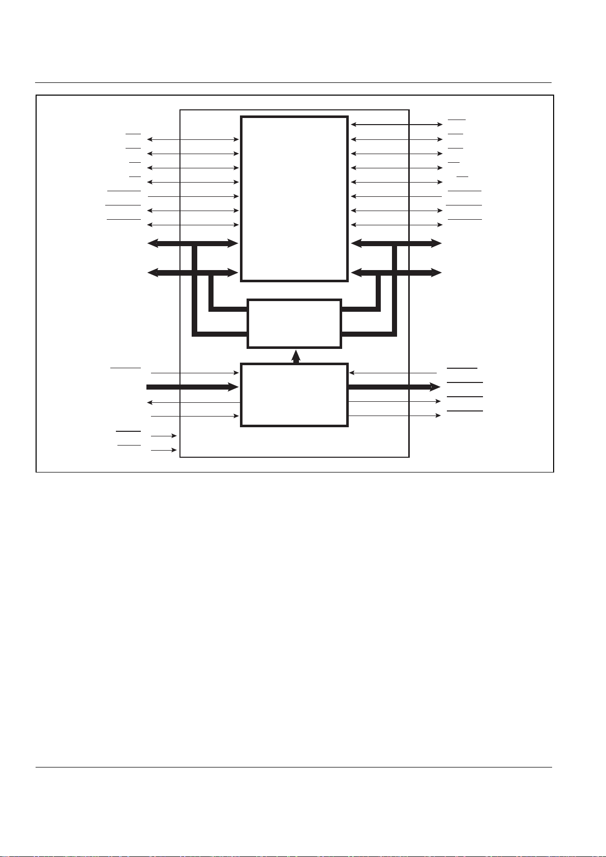
Figure 1. TrailBlazer Functional Block Diagram
PRODUCT OVERVIEW
The IS82C600 TrailBlazer integrates a high-speed 64K x
16 SRAM with a processor port-to-processor port bridge
function. This simplifies any high-speed designs by
providing a fast access time for the processor on the
Primary Port and enabling for a low-cost implementation of
a high-frequency system.
TrailBlazer combines a high-performance memory array,
programmable decodes, and "Ready" logic to achieve
maximum performance and flexibility, while keeping costs
at a minimum. In order to simplify system development,
TrailBlazer duplicates the Primary Bus signals on its
Secondary Bus to permit the use of existing system
components and ASICs together with a new generation of
high-performance processors.
On its Primary Bus, the TrailBlazer provides a high-speed
SRAM interface and then broadcasts the Primary Bus
cycles to its Secondary Bus, allowing the processor on its
Primary Bus to access peripherals on its Secondary Bus.
In many cases, since the peripherals are accessed by the
same signals, existing ASICs can be re-used.
TrailBlazer provides an optimized, seamless interface to
TI TMS320LC54x high-speed processor without the need
for any glue logic interfaces for local peripherals on the
Secondary Bus. TrailBlazer can also be used as shared
Local or Global Memory for a dual processor-based system
where the Chip Select logic on each bus allows for the
same data to be accessed at different locations in memory,
if so desired.
DECODER
SRAM
64K x 16
BUS
REPEATER
PSp
DSp
ISp
R/Wp
HOLDAp
IOSTRBp
MSTRBp
Dp[15:0]
Ap[15:0]
Ds[15:0]
As[15:0]
CSINTp
Ap[21:16]
RDY
CLK
PRGM
XCVR
CSINTs
CSMEMs[5:0]
WEMEMs
OEMEMs
PSs
DSs
ISs
R/Ws
HOLDAs
IOSTRBs
MSTRBs
PSp
DSp
ISp
R/Wp
HOLDAp
IOSTRBp
MSTRBp
WEs
PSs
DSs
ISs
R/Ws
HOLDAs
IOSTRBs
MSTRBs
IS82C600
Integrated Silicon Solution, Inc. — 1-800-379-4774
3
PRELIMINARY TB001-0B
01/20/99
ISSI
®
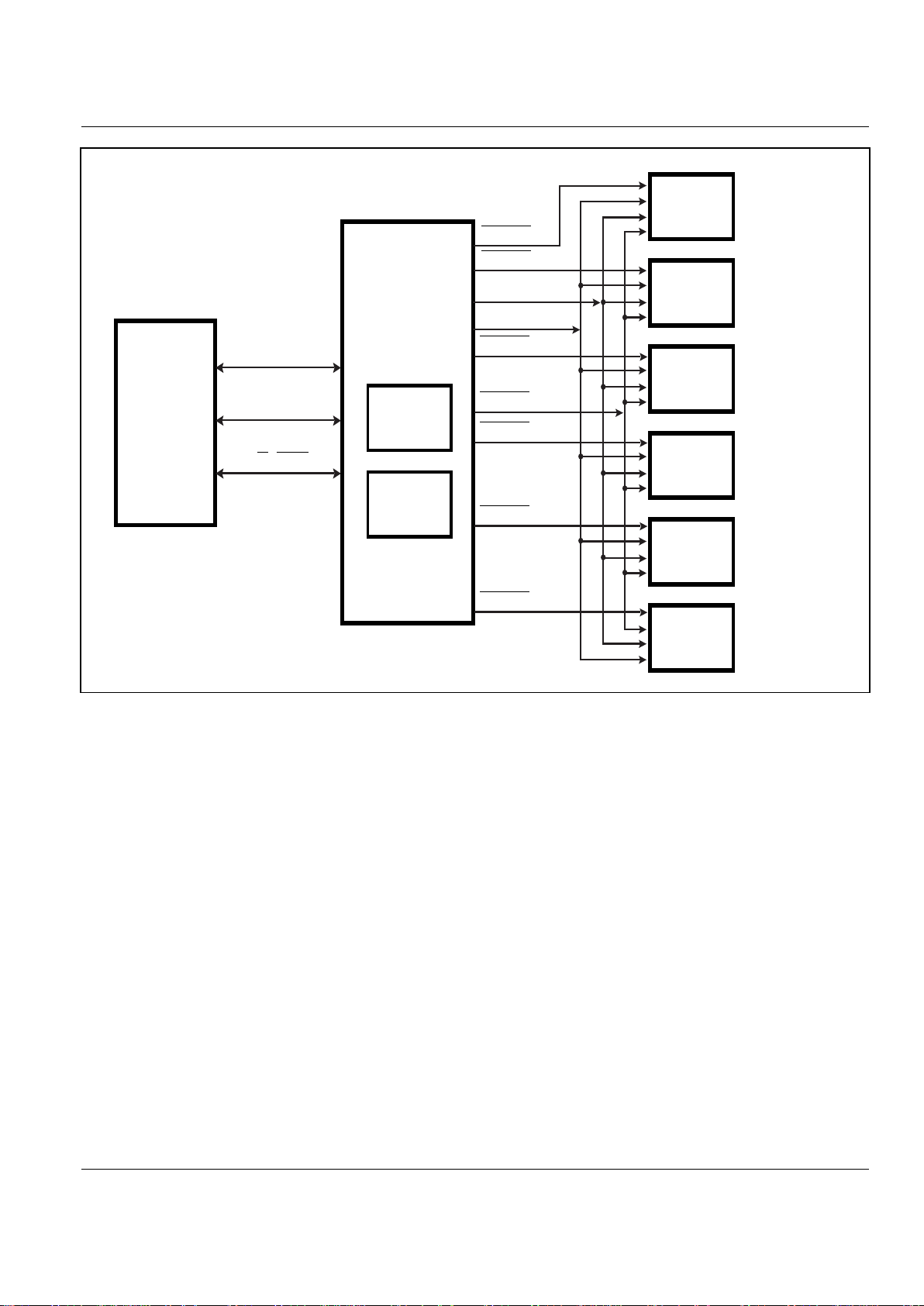
Figure 2. TrailBlazer System Block Diagram with High-Speed DSP on the Primary Bus and
the Slower Existing DSP System Components on the Secondary Bus
DSP
CSMEMs[0]
TRAILBLAZER
IS82C600
LOCAL
DEVICE 1
LOCAL
DEVICE 2
32K x 16
32K x 16
(REGISTER 0) (DEFAULT)
(REGISTER 5)
(REGISTER 4)
(REGISTER 3)
(REGISTER 2)
(REGISTER 1)
LOCAL
DEVICE 3
LOCAL
DEVICE 4
LOCAL
DEVICE 5
LOCAL
DEVICE 6
CSMEMs[1]
As[15:0]
Ap[21:0]
Dp[15:0]
R/W, STRB
Ds[15:0]
CSMEMs[2]
CSMEMs[3]
CSMEMs[4]
CSMEMs[5]
WEMEMs
4
Integrated Silicon Solution, Inc. — 1-800-379-4774
PRELIMINARY TB001-0B
01/20/99
IS82C600
ISSI
®
PIN INFORMATION
Complete pin information on the device is organized as
follows:
• Overview
• Conventions
• Pin Diagram
• Pin Assignment Table—Arranged by Pin Number
• Pin Assignment Table—Arranged by Ball Location
• Detailed Pin Descriptions
Overview
The R/W signal determines the direction of the bus
transaction.
Some processors, including TI TMS320LC54X, have three
major memory spaces. Program Space (PS); Data Space
(DS); and I/O Space (IS). The Memory Space signals (DS,
PS
, and IS) select the memory address space being
accessed (Data, Program, or I/O). No more than one of the
Memory Space signals can be asserted at the same time.
Data or Program spaces (or any part of these spaces) can
be mapped into either internal SRAM of the TrailBlazer or
any external devices. I/O space can only be mapped to
external devices. The TrailBlazer’s internal SRAM has two
32KB regions that are restricted to either DS or PS space.
Register 0 controls the decoding for the internal SRAM.
Registers 1 through 5 control the address decoding for the
external devices on the Secondary Bus. For processors
that have A15 as the MSB, the three memory
spaces are restricted to 64KB each. However, the registers
do allow for programmable address ranges in 8KB blocks.
For processors with A[21:16] as the MSB, there is a 4MB
maximum address space that can be partitioned by
programming Registers 1 to 5.
Chip Selects (
CSMEM
x) are used to select external devices
on the Secondary Bus. These signals are generated by
combinations of the Memory Space signals and Addresses
Ap[13:21].
Strobes (
MSTRB
and
IOSTRB
) validate Memory Space
selections. PS and DS have to be validated by the assertion
of
MSTRB
and IS has to be validated by the assertion of
IOSTRB
.
The following provides detailed technical information
related to the pins on the device. For ease of reference, the
pin information is presented in a table format arranged both
by pin numbers and by pin names. A pin diagram has also
been included to be used as a visual point of reference.
Conventions
Table 1 details conventions that are used to present
information on the pins.
Table 1. Pin Conventions
Convention Meaning
NC This pin is reserved for ISSI, Inc. and must
be left as a 'No Connect'
I Input-only
O Output-only
I/O Input or Output (Bi-directional)
Power Power pin
Ground Ground pin
SIGNAL
Active (or asserted) state occurs when pin
is at a low voltage
/ Multiplexed or Dual functionality
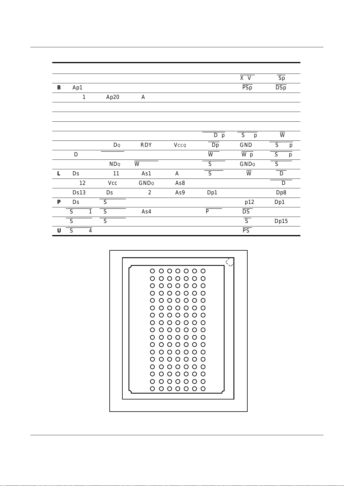
Pin Diagram
Refer to Figure 3 and Table 2 for the pin diagram for the
TrailBlazer device. It depicts the pin names and the
corresponding ball location. Pins marked as 'NC' are not
available and are defined as 'No Connect' pins. For more
detailed information on the pins refer to Table 5.
IS82C600
Integrated Silicon Solution, Inc. — 1-800-379-4774
5
PRELIMINARY TB001-0B
01/20/99
ISSI
®
Figure 3. TrailBlazer Pin Diagram
7654
BOTTOM VIEW
321
A
B
C
D
E
F
G
H
J
K
L
M
N
P
R
T
U
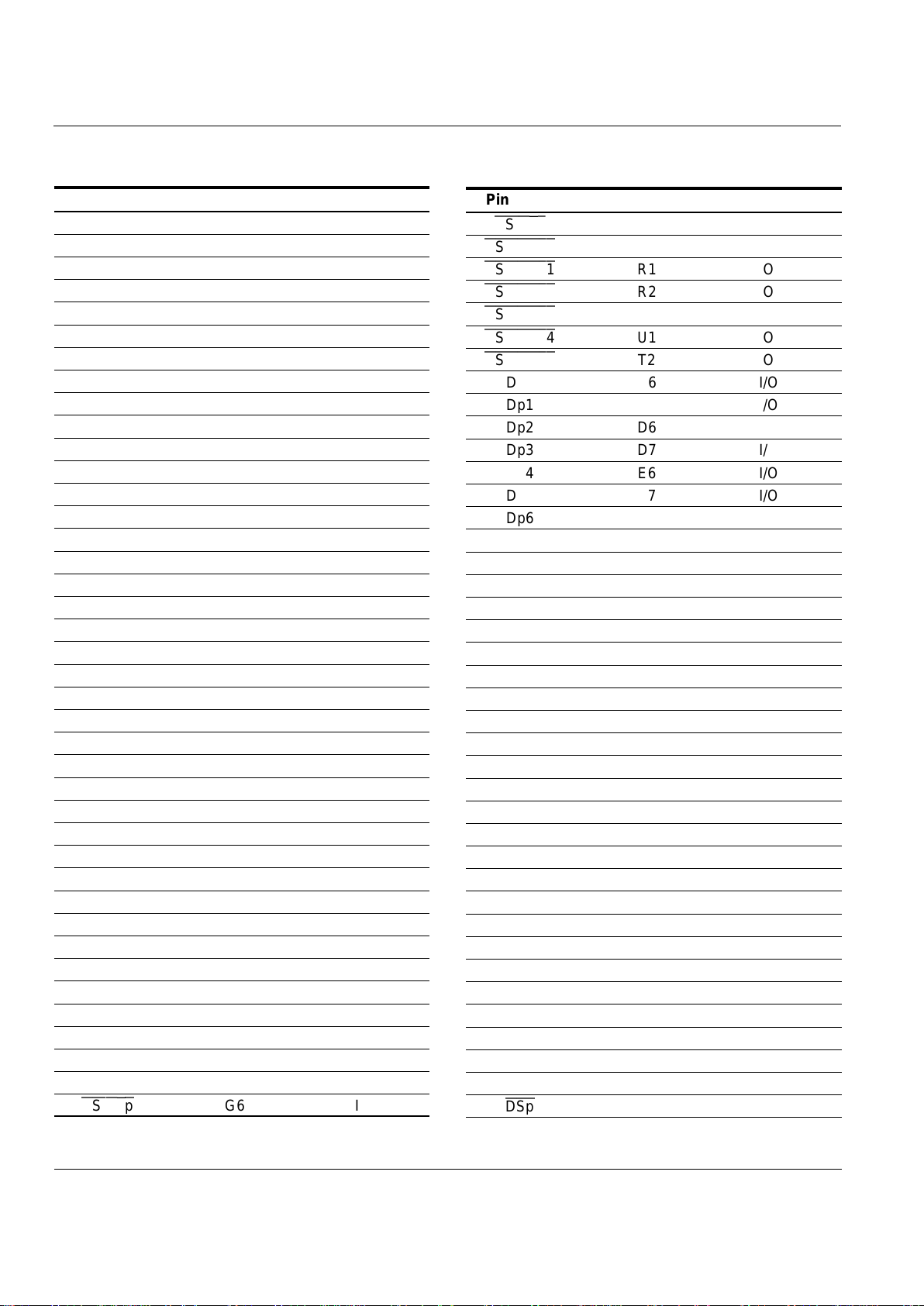
Table 2. Pin Configuration: 119-pin PBGA
1234567
AAp18 Ap16 Ap4 Ap5 Ap11
XCVR ISp
B Ap19 Ap17 Ap3 Ap6 Ap12
PSp DSp
C Ap21 Ap20 Ap2 Ap7 Ap13 Dp0 Dp1
D Ds1 Ds0 Ap1 Ap8 Ap14 Dp2 Dp3
E Ds3 Ds2 Ap0 Ap9 Ap15 Dp4 Dp5
F Ds4 GND GNDQ Ap10 GNDQ VCC Dp6
G Ds7 Ds6 Ds5 Dp7
HOLDAp CSINTp
R/Wp
H CLK GNDQ RDY VCCQ
RDp
GNDQ
IOSTRBp
J Ds8
OEMEMs
VCCQ VCCQ
WEs WEp MSTRBp
K Ds9 GNDQ
WEMEMs
VCCQ
IOSTRBs
GNDQ
MSTRBs
L Ds10 Ds11 As1 As7
CSINTs
R/Ws
RDs
M Ds12 Vcc GNDQ As8 GNDQ GND
HOLDAs
N Ds13 Ds14 As2 As9 Dp10 Dp9 Dp8
P Ds15
CSMEMs0
As3 As10 Dp13 Dp12 Dp11
R
CSMEMs1 CSMEMs2
As4 As11
PRGM DSs
Dp14
T
CSMEMs3 CSMEMs5
As5 As12 As15
ISs
Dp15
U
CSMEMs4
As0 As6 As13 As14
PSs
NC
6
Integrated Silicon Solution, Inc. — 1-800-379-4774
PRELIMINARY TB001-0B
01/20/99
IS82C600
ISSI
®
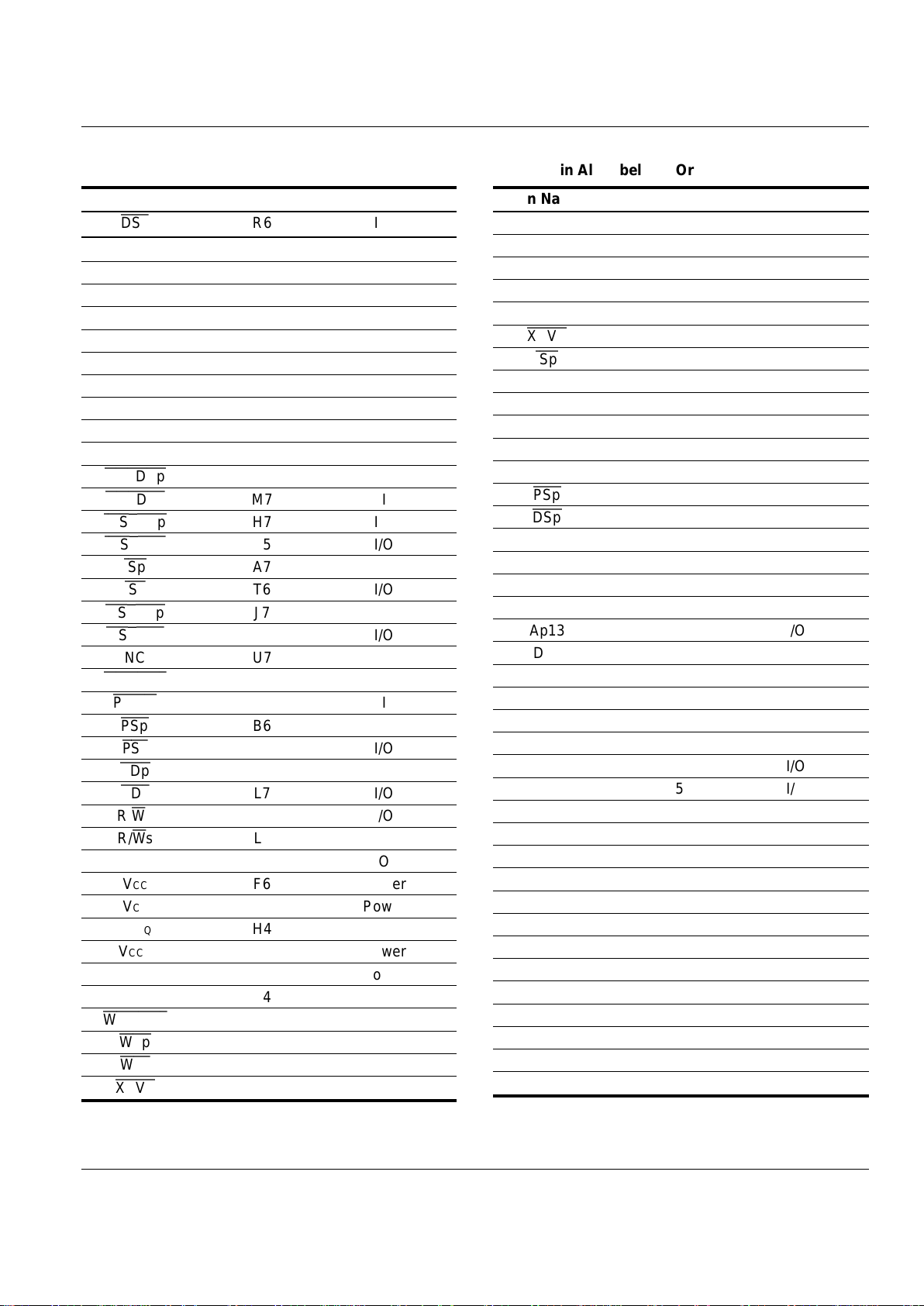
Table 3. Pin Assignment Table—Arranged by Pin
Name in Alphabetical Order
Pin Name Ball Location Pin Type
Ap0 E3 I/O
Ap1 D3 I/O
Ap2 C3 I/O
Ap3 B3 I/O
Ap4 A3 I/O
Ap5 A4 I/O
Ap6 B4 I/O
Ap7 C4 I/O
Ap8 D4 I/O
Ap9 E4 I/O
Ap10 F4 I/O
Ap11 A5 I/O
Ap12 B5 I/O
Ap13 C5 I/O
Ap14 D5 I/O
Ap15 E5 I/O
Ap16 A2 I
Ap17 B2 I
Ap18 A1 I
Ap19 B1 I
Ap20 C2 I
Ap21 C1 I
As0 U2 I/O
As1 L3 I/O
As2 N3 I/O
As3 P3 I/O
As4 R3 I/O
As5 T3 I/O
As6 U3 I/O
As7 L4 I/O
As8 M4 I/O
As9 N4 I/O
As10 P4 I/O
As11 R4 I/O
As12 T4 I/O
As13 U4 I/O
As14 U5 I/O
As15 T5 I/O
CLK H1 I
CSINTp
G6 I
Pin Name Ball Location Pin Type
CSINTs
L5 I
CSMEMs0
P2 O
CSMEMs1
R1 O
CSMEMs2
R2 O
CSMEMs3
T1 O
CSMEMs4
U1 O
CSMEMs5
T2 O
Dp0 C6 I/O
Dp1 C7 I/O
Dp2 D6 I/O
Dp3 D7 I/O
Dp4 E6 I/O
Dp5 E7 I/O
Dp6 F7 I/O
Dp7 G4 I/O
Dp8 N7 I/O
Dp9 N6 I/O
Dp10 N5 I/O
Dp11 P7 I/O
Dp12 P6 I/O
Dp13 P5 I/O
Dp14 R7 I/O
Dp15 T7 I/O
Ds0 D2 I/O
Ds1 D1 I/O
Ds2 E2 I/O
Ds3 E1 I/O
Ds4 F1 I/O
Ds5 G3 I/O
Ds6 G2 I/O
Ds7 G1 I/O
Ds8 J1 I/O
Ds9 K1 I/O
Ds10 L1 I/O
Ds11 L2 I/O
Ds12 M1 I/O
Ds13 N1 I/O
Ds14 N2 I/O
Ds15 P1 I/O
DSp
B7 I/O
IS82C600
Integrated Silicon Solution, Inc. — 1-800-379-4774
7
PRELIMINARY TB001-0B
01/20/99
ISSI
®
Table 3. Pin Assignment Table—Arranged by Pin
Name in Alphabetical Order
(continued)
Pin Name Ball Location Pin Type
DSs
R6 I/O
GND F2 Ground
GND M6 Ground
GNDQ F3 Ground
GNDQ F5 Ground
GNDQ H2 Ground
GNDQ H6 Ground
GNDQ K2 Ground
GNDQ K6 Ground
GNDQ M3 Ground
GNDQ M5 Ground
HOLDAp
G5 I
HOLDAs
M7 I
IOSTRBp
H7 I/O
IOSTRBs
K5 I/O
ISp
A7 I/O
ISs
T6 I/O
MSTRBp
J7 I/O
MSTRBs
K7 I/O
NC U7
OEMEMs
J2 O
PRGM
R5 I
PSp
B6 I/O
PSs
U6 I/O
RDp
H5 I/O
RDs
L7 I/O
R/Wp G7 I/O
R/Ws L6 I/O
RDY H3 O
VCC F6 Power
VCC M2 Power
VCCQ H4 Power
VCCQ J3 Power
VCCQ J4 Power
VCCQ K4 Power
WEMEMs
K3 O
WEp
J6 I/O
WEs
J5 I/O
XCVR
A6 I
Table 4. Pin Assignment Table—Arranged by Ball
Location in Alphabeltical Order
Pin Name Ball Location Pin Type
Ap18 A1 I
Ap16 A2 I
Ap4 A3 I/O
Ap5 A4 I/O
Ap11 A5 I/O
XCVR
A6 I
ISp
A7 I/O
Ap19 B1 I
Ap17 B2 I
Ap3 B3 I/O
Ap6 B4 I/O
Ap12 B5 I/O
PSp
B6 I/O
DSp
B7 I/O
Ap21 C1 I
Ap20 C2 I
Ap2 C3 I/O
Ap7 C4 I/O
Ap13 C5 I/O
Dp0 C6 I/O
Dp1 C7 I/O
Ds1 D1 I/O
Ds0 D2 I/O
Ap1 D3 I/O
Ap8 D4 I/O
Ap14 D5 I/O
Dp2 D6 I/O
Dp3 D7 I/O
Ds3 E1 I/O
Ds2 E2 I/O
Ap0 E3 I/O
Ap9 E4 I/O
Ap15 E5 I/O
Dp4 E6 I/O
Dp5 E7 I/O
Ds4 F1 I/O
GND F2 Ground
GNDQ F3 Ground
Ap10 F4 I/O

8
Integrated Silicon Solution, Inc. — 1-800-379-4774
PRELIMINARY TB001-0B
01/20/99
IS82C600
ISSI
®
Table 4. Pin Assignment Table—Arranged by Ball
Location in Alphabeltical Order
(continued)
Pin Name Ball Location Pin Type
GNDQ F5 Ground
VCC F6 Power
Dp6 F7 I/O
Ds7 G1 I/O
Ds6 G2 I/O
Ds5 G3 I/O
Dp7 G4 I/O
HOLDAp
G5 I
CSINTp
G6 I
R/Wp G7 I/O
CLK H1 I
GNDQ H2 Ground
RDY H3 O
VCCQ H4 Power
RDp
H5 I/O
GNDQ H6 Ground
IOSTRBp
H7 I/O
Ds8 J1 I/O
OEMEMs
J2 O
VCCQ J3 Power
VCCQ J4 Power
WEs
J5 I/O
WEp
J6 I/O
MSTRBp
J7 I/O
Ds9 K1 I/O
GNDQ K2 Ground
WEMEMs
K3 O
VCCQ K4 Power
IOSTRBs
K5 I/O
GNDQ K6 Ground
MSTRBs
K7 I/O
Ds10 L1 I/O
Ds11 L2 I/O
As1 L3 I/O
As7 L4 I/O
CSINTs
L5 I
R/Ws L6 I/O
RDs
L7 I/O
Ds12 M1 I/O
VCC M2 Power
Pin Name Ball Location Pin Type
GNDQ M3 Ground
As8 M4 I/O
GNDQ M5 Ground
GND M6 Ground
HOLDAs
M7 I
Ds13 N1 I/O
Ds14 N2 I/O
As2 N3 I/O
As9 N4 I/O
Dp10 N5 I/O
Dp9 N6 I/O
Dp8 N7 I/O
Ds15 P1 I/O
CSMEMs0
P2 O
As3 P3 I/O
As10 P4 I/O
Dp13 P5 I/O
Dp12 P6 I/O
Dp11 P7 I/O
CSMEMs1
R1 O
CSMEMs2
R2 O
As4 R3 I/O
As11 R4 I/O
PRGM
R5 I
DSs
R6 I/O
Dp14 R7 I/O
CSMEMs3
T1 O
CSMEMs5
T2 O
As5 T3 I/O
As12 T4 I/O
As15 T5 I/O
ISs
T6 I/O
Dp15 T7 I/O
CSMEMs4
U1 O
As0 U2 I/O
As6 U3 I/O
As13 U4 I/O
As14 U5 I/O
PSs
U6 I/O
NC U7 —

IS82C600
Integrated Silicon Solution, Inc. — 1-800-379-4774
9
PRELIMINARY TB001-0B
01/20/99
ISSI
®
Table 5. Primary Bus Pins
Pin Name Pin Type Pin Description
Ap[15:0] I/O ADDRESS: Primary Bus address pins. The Ap[21] is the MSB and Ap[0] is the LSB.
Ap[21:16] I
CLK I CLOCK SIGNAL (Primary): This is the high-speed clock from the processor. Used for
generation of RDY signal.
CSINTp
I INTERNAL SRAM CHIP SELECT SIGNAL (Primary): When asserted, the SRAM
access is guaranteed from the Primary Bus, irrespective of the configuration mode.
Dp[15:0] I/O DATA: Data pins Dp[15] (MSB) through Dp[0] (LSB) connected to the processor on the
Primary Bus.
DSp
I/O DATA SPACE SIGNAL (Primary): When asserted, indicates processor is accessing
the Data Space (DS) memory. It also validates address information on Ap[21:0].
HOLDAp
I HOLD ACKNOWLEDGE SIGNAL (Primary):
HOLDAp
, when asserted, indicates that
the processor or MPU on the Primary Bus is in a Hold state. This also indicates that
Ap[21:0] and Dp[15:0] are tri-stated. Typically, this signal is used in dual-processor
configurations where access to the internal SRAM is guaranteed for the processor on
the Secondary Bus.
IOSTRBp
I/O I/O STROBE (Primary): When asserted, indicates a Primary Bus access to I/O devices.
ISp
I/O I/O SP ACE SIGNAL (Primary): When asserted, indicates that processor is accessing
the I/O Space (IS). It also validates the address.
MSTRBp
I/O MEMORY STROBE (Primary): When asserted, indicates bus access to data or program
memory .
PSp
I/O PROGRAM SPACE SIGNAL (Primary): When asserted, indicates processor is
communicating with Program Space (PS) memory. It also validates the address.
RDp
I/O This pin should be pulled HIGH.
R/Wp I/O READ/WRITE SIGNAL (Primary): R/W indicates transfer direction during access from
Primary Bus. Set HIGH for a Read and LOW for a Write access.
WEp
I/O This pin should be pulled HIGH.

10
Integrated Silicon Solution, Inc. — 1-800-379-4774
PRELIMINARY TB001-0B
01/20/99
IS82C600
ISSI
®
Table 6. Secondary Bus Pins
Pin Name Pin Type Pin Description
As[15:0] I/O ADDRESS: Secondary Bus address pins. As[15] is the MSB and As[0] is the LSB.
CSINTs
I INTERNAL SRAM CHIP SELECT SIGNAL (Secondary): When asserted, the SRAM
access is guaranteed from the Secondary Bus (if
HOLDAp
= 0), irrespective of the
configuration mode.
CSMEMs[5:0]
O EXTERNAL MEMORY CHIP SELECTS (Secondary): Selects devices on the
Secondary Bus. Refer to the Register Definition Section for more details.
DSs
I/O DAT A SP ACE SIGNAL (Secondary): When asserted, indicates processor is accessing
the Data Space (DS) memory. It also validates address information on As[15:0].
HOLDA
sIHOLD ACKNOWLEDGE SIGNAL (Secondary):
HOLDA
s, when asserted, indicates
that the processor or MPU on the Secondary Bus is in a Hold state. This also indicates
that As[15:0] and Ds[15:0] are tri-stated. Typically , this signal is used in dual-processor
configurations where access to the internal SRAM is guaranteed for the processor on
the Secondary Bus.
IOSTRBs
I/O I/O STROBE (Secondary): When asserted, indicates a Secondary Bus access to I/O
devices.
ISs
I/O I/O SPACE SIGNAL (Secondary): When asserted, indicates that processor is accessing
the I/O space (IS). It also validates the address.
MSTRBs
I/O MEMORY STROBE (Secondary): When asserted, indicates bus access to data or
program memory.
PSs
I/O PROGRAM SPACE SIGNAL (Secondary): When asserted, indicates processor is
communicating with Program Space (PS) memory. It also validates the address.
RDs
I/O This pin should be pulled HIGH.
R/Ws I/O READ/WRITE SIGNAL (Secondary): R/W indicates transfer direction during access
from Secondary Bus. Set HIGH for a Read access and LOW for a Write access.
WEs
I/O This should be pulled HIGH.
WEMEMs
O EXTERNAL MEMORY WRITE ENABLE: This is the memory Write Enable signal for
external memory or peripherals on the Secondary Bus.
Table 7. Miscellaneous Pins
Pin Name Pin Type Pin Description
PRGM
I PROGRAM ENABLE: This signal latches the Secondary Address Bus, As[15:0], on its
rising edge. Typically, the
PRGM
is derived from
RESET
so that upon power-up, the
state of As[15:0] is latched. As[15:8] determine the mode of internal SRAM decode and
external memory decoding for the Secondary Bus. (See Register Descriptions for more
detail.)
RDY O RDY is asserted whenever a Secondary Bus device is able to communicate with the
TrailBlazer . RDY is programmed in Register 6 for various DS, IS, and PS memory address
spaces.
XCVR
I TRANSCEIVER MODE: This pin puts the TrailBlazer into a transceiver-like mode to
support the processor's DMA through the TrailBlazer, e.g., when a Primary Bus wants
to read the data on the Secondary Bus. In this mode, the
XCVR
is asserted, and the
HOLDAs
pin must be LOW, indicating no processors are on the Secondary Bus and the
Primary Bus processor can read from the peripheral (or memory) from the Secondary
Bus. (See Table 8, Bus Logic Truth Table for every possible combination.)
VCCQ Power Power pins for I/O buffers of TrailBlazer.
GNDQ Ground Ground pins for I/O buffers of TrailBlazer.
VCC Power Power pins for core of TrailBlazer.
GND Ground Ground pins for core of TrailBlazer
Note: 1. Typically, VCC and VCCQ are at 3.3 Volts.

IS82C600
Integrated Silicon Solution, Inc. — 1-800-379-4774
11
PRELIMINARY TB001-0B
01/20/99
ISSI
®
Table 8. Bus Logic Truth Table
XCVRXCVR
XCVRXCVR
XCVR
HOLDAHOLDA
HOLDAHOLDA
HOLDA
p
HOLDAHOLDA
HOLDAHOLDA
HOLDA
s
CSINTCSINT
CSINTCSINT
CSINT
p
CSINTCSINT
CSINTCSINT
CSINT
s Action
CSMEMCSMEM
CSMEMCSMEM
CSMEM
s[5:0]
0 0 X X X Transceiver R/W of
CSMEM
s[5:0]
Primary Bus by are not asserted.
Secondary Bus (DMA). .
0 1 X X X Transceiver R/W of
CSMEM
s[5:0]
Secondary Bus by are not asserted.
Primary Bus (DMA).
10 XX 0 R/
W
of Internal SRAM by
CSMEM
s[5:0]
the Secondary Bus only. are not asserted
11 0 0 X R/
W
of Internal SRAM by
CSMEM
s[5:0]
the Primary Bus only. are not asserted
1 1 0 1 X Primary Bus is in One of
CSMEM
s[5:0]
control. R/W from asserted, depending on
external or internal Ap[21:13] and PSp,
memory by Primary
DS
p and ISp.
Bus. Control signals
are forward to the
Secondary Bus.
11 1 0 X R/
W
of Internal SRAM by
CSMEM
s[5:0]
the Primary Bus only. are not asserted
Control signals are not
forwarded to the Secondary
Bus. Secondary Bus access
to internal memory denied.
11 1 1 X R/
W
of internal
CSMEM
s[5:0]
SRAM by Primary are not asserted
Bus. Control signals Internal SRAM
are not forwarded selection is based on
to the Secondary Bus. Ap[21:13], PSp and DSp
Secondary Bus access to
internal memory denied.
Figure 4. TrailBlazer Interface with TMS320LC54x DSP.
TRAILBLAZER
IS82C600
64K x 16
SRAM
HOLDAs
CSINTp
RDp
WEp
R/Wp
MSTRBp
IOSTRBp
HOLD
CSINT
R/W
MSTRB
IOSTRB
Vcc
Vcc
HOLDAp
A[15:0]
D[15:0]

12
Integrated Silicon Solution, Inc. — 1-800-379-4774
PRELIMINARY TB001-0B
01/20/99
IS82C600
ISSI
®
REGISTER DEFINITIONS
A set of I/O addresses is reserved in the system and is
used for TrailBlazer registers. As[15:8], when sampled by
the rising edge of
PRGM
, determine the displacement of
the starting address for the registers from location 00. A
block of 256 addresses from the starting address is not
available for the system. For example, if As[15:8] are
sampled as 80 (i.e., As[15] pulled HIGH and As[14:8]
pulled LOW) the starting I/O address is 8000h and I/O
address 8000h to( 80+255)h are reserved. Register 0 of
TrailBlazer maps to 80 and Register 1 maps to 81, and so
on. Currently, eight registers are defined and the remaining
registers are reserved.
All these registers will come up in their predetermined
default states during power-up.
Upon power-up, the mode registers are loaded by sampling
the As[15:0] (Secondary Address Bus). These bits are
sampled on the rising edge of the
PRGM
. The
PRGM
pin
can be controlled in several different ways. The simpliest
method is to tie the pin to the RESET pulse of the
processor. When
PRGM
is asserted, the entire chip will be
tri-stated and, therefore, normal functionality cannot be
maintained while this pin is active. If the system requires
a “dynamic” decoding of the address bits, the XF pin from
the processor can be used as a gate to the decoding latch.
Register 0
TrailBlazer SRAM Decode Register (default FFFF)
This register is used to set the base address for each of the
two 32K x 16 blocks of TrailBlazer SRAM. Register 0 bits
6:0 are used for setting the starting address of a 32K block
of SRAM and bit 7 determines if this block corresponds for
PS
or DS. When the DS/PS bit is 0, the block is in DS space
and if 1, the block is in PS space. Similarly, bits 15:8
programs the other 32K block.
15 14 13 12 11 10 09 08 07 06 05 04 03 02 01 00
DSDS
DSDS
DS
/
PSPS
PSPS
PS
A21 A20 A19 A18 A17 A16 A15
DSDS
DSDS
DS
/
PSPS
PSPS
PS
A21 A20 A19 A18 A17 A16 A15
Register 1
CSMEMs0CSMEMs0
CSMEMs0CSMEMs0
CSMEMs0
Pin Select Register (default 0008)
This register is used to select the decoding for
CSMEM
s0.
The decoding is on an 8K boundary and can be
programmed to respond to PS, DS, or IS address space or
a combination thereof. The
CSMEM
s0 can be used as a
chip select pin for external memory or I/O device.
Register 1 bits D[14:6] are used to set the base address
for which the decode occurs, bits 5:3 determine the space,
PS, DS
, or IS, and bits 2:0 determine the size of the
decode. Bit 15 is a reserved bit. On power-up, the register
will reset at the default state of 0008.
15 14 13 12 11 10 09 08 07 06 05 04 03 02 01 00
RSVD A21 A20 A19 A18 A17 A16 A15 A14 A13
PSPS
PSPS
PS
DSDS
DSDS
DS
ISIS
ISIS
IS
SZ2 SZ1 SZ0
Bits 14 to 6 correspond to address bits A21 to A13 and sets the starting address for which
CSMEM
s0 is active.
Bits 5 to 3 determine the space for which the pin will be active which are encoded as follows:
Bits 2 to 0 determine the size for which
CSMEM
s0 will be active starting from address as determined by bits 14 to
6. RSRVD bit should always be programmed to ZERO.

IS82C600
Integrated Silicon Solution, Inc. — 1-800-379-4774
13
PRELIMINARY TB001-0B
01/20/99
ISSI
®
PSPS
PSPS
PS
DSDS
DSDS
DS
ISIS
ISIS
IS
Space for which
CSMEMs0CSMEMs0
CSMEMs0CSMEMs0
CSMEMs0
will be active
000
CSMEMs0
will not respond to any space, i.e., disabled.
001
CSMEMs0
will be asserted for I/O space (when IS asserted) as determined by the
starting address and size bits.
010
CSMEMs0
will be asserted for DATA space (when DS asserted) as determined by
the starting address and size bits.
011
CSMEMs0
will be asserted for I/O or DATA space (when IS or DS asserted) as
determined by the starting address and size bits.
100
CSMEMs0
will be asserted for PROGRAM space (when PS asserted) as determined
by the starting address and size bits.
101
CSMEMs0
will be asserted for PROGRAM or I/O space (when PS or IS asserted) as
determined by the starting address and size bits.
110
CSMEMs0
will be asserted for PROGRAM or DATA space (when PS or DS asserted)
as determined by the starting address and size bits.
111
CSMEMs0
will be asserted for any space as determined by the starting address and
size bits.
Size for which
CSMEMs0CSMEMs0
CSMEMs0CSMEMs0
CSMEMs0
will be active starting from the programmed starting
SZ2 SZ1 SZ0
address. The sizes are in the increments of 8K Words.
00 0
CSMEMs0
will be asserted for starting address to starting address + 8K
00 1
CSMEMs0
will be asserted for starting address to starting address + 16K
01 0
CSMEMs0
will be asserted for starting address to starting address + 32K
01 1
CSMEMs0
will be asserted for starting address to starting address + 64K
10 0
CSMEMs0
will be asserted for starting address to starting address + 128K
10 1
CSMEMs0
will be asserted for starting address to starting address + 256K
11 0
CSMEMs0
will be asserted for starting address to starting address + 512K
11 1
CSMEMs0
will be asserted for starting address to starting address + 1024K
Register 2
CSMEMs1CSMEMs1
CSMEMs1CSMEMs1
CSMEMs1
Pin Select Register (default 0048):
This register is used to select the decoding for
CSMEM
s1.
The decoding is on an 8K boundary and can be programmed
to respond to PS, DS, or IS address space or a combination
thereof. The
CSMEM
s0 can be used as chip select pin for
external memory or I/O device. The bit descriptions and
programmability are identical to Register 1, except that the
default is 0048. Refer to
CSMEM
s0 bit descriptions.
15 14 13 12 11 10 09 08 07 06 05 04 03 02 01 00
RSVD A21 A20 A19 A18 A17 A16 A15 A14 A13
PSPS
PSPS
PS
DSDS
DSDS
DS
ISIS
ISIS
IS
SZ2 SZ1 SZ0

14
Integrated Silicon Solution, Inc. — 1-800-379-4774
PRELIMINARY TB001-0B
01/20/99
IS82C600
ISSI
®
Register 3
CSMEMs2CSMEMs2
CSMEMs2CSMEMs2
CSMEMs2
Pin Select Register (default 0088):
This register is used to select the decoding for
CSMEM
s2.
The decoding is on an 8K boundary and can be programmed
to respond to PS, DS, or IS address space or a combination
thereof. The
CSMEM
s2 can be used as a chip select pin for
external memory or I/O device. The bit descriptions and
programmability are identical to Register 1, except that the
default is 0088. Refer to
CSMEM
s0 bit descriptions.
15 14 13 12 11 10 09 08 07 06 05 04 03 02 01 00
RSVD A21 A20 A19 A18 A17 A16 A15 A14 A13
PSPS
PSPS
PS
DSDS
DSDS
DS
ISIS
ISIS
IS
SZ2 SZ1 SZ0
Register 4
CSMEMs3CSMEMs3
CSMEMs3CSMEMs3
CSMEMs3
Pin Select Register (default 00C8):
This register is used to select the decoding for
CSMEM
s3.
The decoding is on an 8K boundary and can be programmed
to respond to PS, DS, or IS address space or a combination
thereof. The
CSMEM
s3 can be used as a chip select pin for
external memory or I/O device The bit descriptions and
programmability are identical to Register 1, except that the
default is 00C8. Refer to
CSMEM
s0 bit descriptions.
15 14 13 12 11 10 09 08 07 06 05 04 03 02 01 00
RSVD A21 A20 A19 A18 A17 A16 A15 A14 A13
PSPS
PSPS
PS
DSDS
DSDS
DS
ISIS
ISIS
IS
SZ2 SZ1 SZ0

IS82C600
Integrated Silicon Solution, Inc. — 1-800-379-4774
15
PRELIMINARY TB001-0B
01/20/99
ISSI
®
Register 5
CSMEMs4CSMEMs4
CSMEMs4CSMEMs4
CSMEMs4
Pin Select Register (default 0112):
This register is used to select the decoding for
CSMEM
s4.
The decoding is on an 8K boundary and can be
programmed to respond to DS or IS address space or a
combination thereof. The
CSMEM
s4 can be used as a chip
select pin for external memory or I/O device. The bit
descriptions and programmability are identical to Register
1, except that the default is 0112. Refer to
CSMEM
s0 bit
descriptions.
15 14 13 12 11 10 09 08 07 06 05 04 03 02 01 00
RSVD RSVD RSVD RSVD RSVD RSVD RSVD A15 A14 A13 RSVD
DSDS
DSDS
DS
ISIS
ISIS
IS
RSVD SZ1 SZ0
DSDS
DSDS
DS
ISIS
ISIS
IS
Space for which
CSMEMs4CSMEMs4
CSMEMs4CSMEMs4
CSMEMs4
will be active
00
CSMEMs0
will not respond to any space, i.e., disabled.
01
CSMEMs0
will go active for I/O space (when IS is active) as determined by the starting
address and size bits.
10
CSMEMs0
will go active for DATA space (when DS is active) as determined by the starting
address and size bits.
11
CSMEMs0
will go active for I/O or DATA space (when IS or DS is active) as determined by
the starting address and size bits.
Size for which
CSMEMs4CSMEMs4
CSMEMs4CSMEMs4
CSMEMs4
will be active starting from the programmed starting
SZ1 SZ0
address. The sizes are in the increments of 8K Words.
00
CSMEMs0
will be active for starting address to starting address + 8K
01
CSMEMs0
will be active for starting address to starting address + 16K
10
CSMEMs0
will be active for starting address to starting address + 32K
11
CSMEMs0
will be active for starting address to starting address + 64K
CSMEMs5CSMEMs5
CSMEMs5CSMEMs5
CSMEMs5
Pin Select Register
This is a negative decode of the other chip selects, i.e., it
is active when
CSMEM
s[4:0] are HIGH.
\

16
Integrated Silicon Solution, Inc. — 1-800-379-4774
PRELIMINARY TB001-0B
01/20/99
IS82C600
ISSI
®
Register 6
RDY Generation Logic and Write Control Register
(default FFFF):
Register 6 is the signal RDY generation register for PS, DS,
and IS space. PS[4:0] (bits 4:0) determine the number of
clocks after which the RDY is generated whenever
PS
goes active. Similarly, DS[4:0] are used to program the
RDY generation in number of clocks when DS is active and
IS
[4:0] are used to generate the RDY for I/O cycles. The
RDY signal could be used to delay an access to an external
device on the Secondary Bus. Please note that if an
external RDY has to be sampled by the processor, the
processor’s access should be programmed for at least two
wait states.
15 14 13 12 11 10 09 08 07 06 05 04 03 02 01 00
WEWE
WEWE
WE
IS4 IS3 IS2 IS1 IS0 DS4 DS3 DS2 DS1 DS0 PS4 PS3 PS2 PS1 PS0
Notes:
1. The above registers are read/writable.
2. No
CSMEMs
will be active if the I/O address of the registers matches with any
CSMEMs
decodes.
Table 9. Register Accessibility
Register Number Register Address Register Compare Data Chip Select
0 Ap[15:8] = SA Ap[21:15]; DSp; PSp Internal SRAM
1 Ap[15:8] = SA+1 Ap[21:13]; DSp; PSp; Isp
CSMEM
s0
2 Ap[15:8] = SA+2 Ap[21:13]; DSp; PSp; ISp
CSMEM
s1
3 Ap[15:8] = SA+3 Ap[21:13]; DSp; PSp; ISp
CSMEM
s2
4 Ap[15:8] = SA+4 Ap[21:13]; DSp; PSp; ISp
CSMEM
s3
5 Ap[15:8] = SA+5 Ap[15:13]; DSp; ISp
CSMEM
s4
6 Ap[15:8] = SA+6
DS
p; PSp; ISp
CSMEM
s5
Notes:
1. SA = Starting address as defined by As[15:8] on the rising edge of
PRGM
.
2. Register write data: Dp[15:0].
3. Register write control:
IOSTRB
p • (R/Wp) • ISp. Some processors, including TI TMS320LC54X, have three major memory
spaces. Program Space (PS signal); Data space (DS signal); and I/O space (IS signal). The TrailBlazer’s internal SRAM has
two 32KB regions that are restricted to either DS or PS space. Register 0 controls the decoding for the internal SRAM. Registers
1 through 5 control the address decoding for the external devices on the Secondary Bus. For processors that have A15 as the
MSB, the three memory spaces are restricted to 64MB each. However, the registers do allow for programmable address ranges
in 8KB blocks. For processors with A[21:16] as the MSB, there is a 4MB maximum address space that can be partitioned by
programming Registers 1 to 5.

IS82C600
Integrated Silicon Solution, Inc. — 1-800-379-4774
17
PRELIMINARY TB001-0B
01/20/99
ISSI
®
ELECTRICAL SPECIFICATIONS
Absolute Maximum Ratings
Symbol Parameters Ratings Units
VCC Supply Voltage –0.4 to 4.1 V
TSTG Storage Temperature –65 to +150 °C
PT Power Dissipation 1.5 W
IOUT DC Output Current (Low) 20 mA
Note:
1. Stresses above the absolute maximum ratings can cause permanent damage to the device.
DC Electrical Characteristics (Over Operating Range)
Symbol Parameter Test Conditona Min Max Units
VOH Output High Voltage Vcc = Min., IOH = –4.0 mA 2.4 — V
VOL Output Low Voltage Vcc = Min., IOL = 8.0 mA — 0.4 V
VIH Input High Voltage 2.2 Vcc + 0.3 V
VIL Input Low Voltage
(1)
0.3 0.8 V
ILI Input Leakage GND ≤ VIN ≤ VCC –2 2 µA
ILO Output Leakage GND ≤ VOUT ≤ VCC, Outputs Disabled –2 2 µA
Note:
1. V
IL(min) = –2.0V for pulse width less than 10 µs.
AC Specification: 25 pF Load
Internal SRAM Cycles Primary Bus Master
-8 -9 -10
T# Parameter Min Max Min Max Min Max Units
T1 Data Access Time from
RDp
LOW — 5 — 5.5 — 6 ns
T2 Data Access Time from Address Valid (5X CPU) — 8 — 9 — 10 ns
T3 Data Access Time from Address (54X CPU) — 8 — 9 — 10 ns
T4 Data Access Time from
PS/DS/IS
—8 —9 —10 ns
T5 Data Access Time from
MSTRBp
—5 —5.5 —6 ns
T6 Data Access Time from
CSINTp
—6 —6.5 —7 ns
T7 Address to
WEp
Valid 1 — 1 — 1 — ns
T8 Write Data Setup Time before
WEp
HIGH 4 — 4 — 4 — ns
T9 Write Data Hold Time after
WEp
HIGH 0 — 0 — 0 — ns
T10 Write Data Setup Time before
MSTRB
HIGH 4 — 4 — 4 — ns
T11 Write Data Hold Time after
MSTRB
HIGH 0 — 0 — 0 — ns
Operating Range
Range Ambient Temperature Vcc
Commercial 0°C to +70°C 3.0V to 3.6V
Industrial –40°C to +85°C 3.0V to 3.6V

18
Integrated Silicon Solution, Inc. — 1-800-379-4774
PRELIMINARY TB001-0B
01/20/99
IS82C600
ISSI
®
Primary Bus Master Local Mode
T# Parameter Min Max Min Max Min Max Units
T12
MSTRBp
/
IOSTRBp
Active to 0 5 0 5.5 0 6 ns
OEMEMp
Active Delay
T13
WEp
Active to
WMEMp
Active Delay 0 5 0 5.5 0 6 ns
T14
MSTRBp
/
IOSTRBp
Active to
WEMEMp
Delay 0 5 0 5.5 0 6 ns
T15
PSp
/
DSp
/
ISp
Active to
CSMEMp
[5:0] Delay 0 5 0 5.5 0 6 ns
Primary Bus Master Remote Mode (Non-
XCVRXCVR
XCVRXCVR
XCVR
Mode)
T# Parameter Min Max Min Max Min Max Units
T16 R/Wp,
PSp, DSp, ISp, MSTRBp, IOSTRBp, RDp
, 0 5 0 5.5 0 6 ns
WEp
Delay to corresponding control signals on
Secondary Bus
T17 Dp to Ds Write Mode (R/W=0) 0 5 0 5.5 0 6 ns
T18 Ds to Dp Read Mode (R/W=1) 0 5 0 5.5 0 6 ns
T19
MSTRBp
/
IOSTRBp
Active to
OEMEMs
Active Delay 0 5 0 5.5 0 6 ns
T20
WEp
Active to
WEMEMs
Active Delay 0 5 0 5.5 0 6 ns
T21
MSTRB
/
IOSTRBp
Active to
WEMEMs
Delay 0 5 0 5.5 0 6 ns
T22
PSp
/
DSp
/
ISp
Active to
CSMEMs
[5:0] Delay 0 5 0 5.5 0 6 ns
Primary Bus Master
XCVRXCVR
XCVRXCVR
XCVR
Mode
T# Parameter Min Max Min Max Min Max Units
T23 R/Wp,
PSp, DSp, ISp, MSTRBp, IOSTRBp, RDp
,030303ns
WEp
Delay to corresponding control signals on
Secondary Bus
T24 Ds to Dp Delay (R/W=HIGH) Read 0 5 0 5.5 0 6 ns
from Secondary Bus
T25 Dp to Ds Delay (R/W=0) Write to Secondary Bus 0 5 0 5.5 0 6 ns
Note:
1. In the above list, the timing parameters are specified with the Primary Bus Master as the basis.

IS82C600
Integrated Silicon Solution, Inc. — 1-800-379-4774
19
PRELIMINARY TB001-0B
01/20/99
ISSI
®
READ CYCLE 1: Primary Bus Internal SRAM READ Cycle Timing (TI TMS320LC5x/C5x DSP)
CLKOUT
(from DSP)
Ap[15:0]
CSINTp, PSp,
DSp, ISp
RDp
Dp[15:0]
DATA VALID
ADDRESS VALID
T2
T1
READ CYCLE 2: Primary Bus Internal SRAM READ Cycle Timing (TI TMS320LC54x/C54x DSP)
CLKOUT
(from DSP)
Ap[15:0]
CSINTp, PSp,
DSp, ISp
MSTRBp
R/Wp = 1
Dp[15:0]
ADDRESS VALID
T5
T4
T3
T6
DATA VALID

20
Integrated Silicon Solution, Inc. — 1-800-379-4774
PRELIMINARY TB001-0B
01/20/99
IS82C600
ISSI
®
WRITE CYCLE 1: Primary Bus Internal SRAM WRITE Cycle Timing (TI TMS320LC5x/C5x DSP)
WRITE CYCLE 2: Primary Bus Internal SRAM WRITE Cycle Timing (TI TMS320LC54x/C54x DSP)
Ap[15:0]
WEp
Dp[15:0]
DATA VALID
ADDRESS VALID
T7
T8 T9
CLKOUT
(from DSP)
Ap[15:0]
MSTRBp
R/Wp
Dp[15:0]
ADDRESS VALID
T10 T11
DATA VALID
Note:
1. All timings are at zero wait state. However, external Writes require two cycles to prevent external bus conflicts.
(Refer to the TI TMS320LC54x/C54x Databook.)
Note:
1. All timings are at zero wait state. However, external Writes require two cycles to prevent external bus conflicts.
(Refer to the TI TMS320LC54x/C54x Databook.)

IS82C600
Integrated Silicon Solution, Inc. — 1-800-379-4774
21
PRELIMINARY TB001-0B
01/20/99
ISSI
®
Primary Bus Control Signals for
OEMEMpOEMEMp
OEMEMpOEMEMp
OEMEMp
,
WEMEMpWEMEMp
WEMEMpWEMEMp
WEMEMp
, and
CSMEMpCSMEMp
CSMEMpCSMEMp
CSMEMp
[5:0]
Primary Bus to Secondary Bus Delay
Note:
1. Tx1 = Timings from T12 through T15.
MSTRBp, IOSTRBp,
WEp, PSp, DSp, ISp
OEMEMp, WEMEMp,
CSMEMp
Tx1
MSTRBp, IOSTRBp, R/Wp,
RDp, PSp, DSp, ISp
WEp, Dp
OEMEMp, WEMEMp,
WEMEMs, CSMEMp, Ds
Tx2
Note:
1. Tx2 = Timings from T16 through T25.
ORDERING INFORMATION
Commercial Range: 0°C to +70°C
Speed (ns) Order Part Number Package
8 IS82C600-8B PBGA
9 IS82C600-9B PBGA
10 IS82C600-10B PBGA
ORDERING INFORMATION
Industrial Range: –40°C to +85°C
Speed (ns) Order Part Number Package
8 IS82C600-8BI PBGA
9 IS82C600-9BI PBGA
10 IS82C600-10BI PBGA
ISSI
®
Integrated Silicon Solution, Inc.
2231 Lawson Lane
Santa Clara, CA 95054
Tel: 1-800-379-4774
Fax: (408) 588-0806
E-mail: sales@issi.com
www.issi.com
 Loading...