

Datasheet IS61NW6432-6PQ, IS61NW6432-5TQ, IS61NW6432-5PQ, IS61NW6432-8TQ, IS61NW6432-8PQ Datasheet (ISSI)
...
IS61NW6432
IS61NW6432
®
ISSI
64K x 32 SYNCHRONOUS STATIC RAM
WITH NO-WAIT STATE BUS FEATURE
FEATURES
• Fast access time:
– 5 ns-100 MHz; 6 ns-83 MHz;
– 7 ns-75 MHz; 8 ns-66 MHz
• No wait cycles between Read and Write
• Internal self-timed write cycle
• Individual Byte Write Control
• Clock controlled, registered address, data and
control
• Pentium™ or linear burst sequence control
using MODE input
• Three chip enables for simple depth expansion
and address pipelining
• Common data inputs and data outputs
• JEDEC 100-pin TQFP and PQFP package
• Single +3.3V power supply
• Optional data strobe pin (#80) for latching data
(See page 12 for detailed timing)
DESCRIPTION
The IS61NW6432 is a high-speed, low-power synchronous
static RAM designed to provide a burstable, highperformance, 'no-wait' bus, secondary cache for the Pentium,
680X0, and Power PC microprocessors. It is organized as
65,536 words by 32 bits, fabricated with ISSI's advanced
CMOS technology.
Incorporating a 'no-wait' bus, wait cycles are eliminated when
the bus switches from read to write, or write to read. This
device integrates a 2-bit burst counter, high-speed SRAM
core, and high-drive capability outputs into a single monolithic
circuit.
All synchronous inputs pass through registers controlled by a
positive-edge-triggered clock input. Operations may be
suspended and all synchronous inputs ignored when Clock
Enable,
their previous values.
When the ADV/LD is HIGH the internal burst counter is
incremented. New external addresses can be loaded when
ADV/LD is LOW.
Write cycles are internally self-timed and are initiated by the
rising edge of the clock inputs and when RD/WE is LOW.
Separate byte enables allow individual bytes to be written.
BW1
I/O17-I/O24;
when
CEN
is HIGH. In this state the internal device will hold
controls I/O1-I/O8;
BW4
BW1, BW2, BW3
ADVANCE INFORMATION
JULY 1998
BW2
controls I/O9-I/O16;
controls I/O25-I/O32. All Bytes are written
, and
BW4
are LOW.
BW3
controls
MODE pin upon power up is in interleave burst mode. It can be
connected to GNDQ or VCCQ to alter power up state.
This document contains ADVANCE INFORMATION data. ISSI reserves the right to make changes to its products at any time without notice in order to improve design and supply the best possible
product. We assume no responsibility for any errors which may appear in this publication. © Copyright 1998, Integrated Silicon Solution, Inc.
Integrated Silicon Solution, Inc.
ADVANCE INFORMATION SR050-0B
07/15/98
1
IS61NW6432
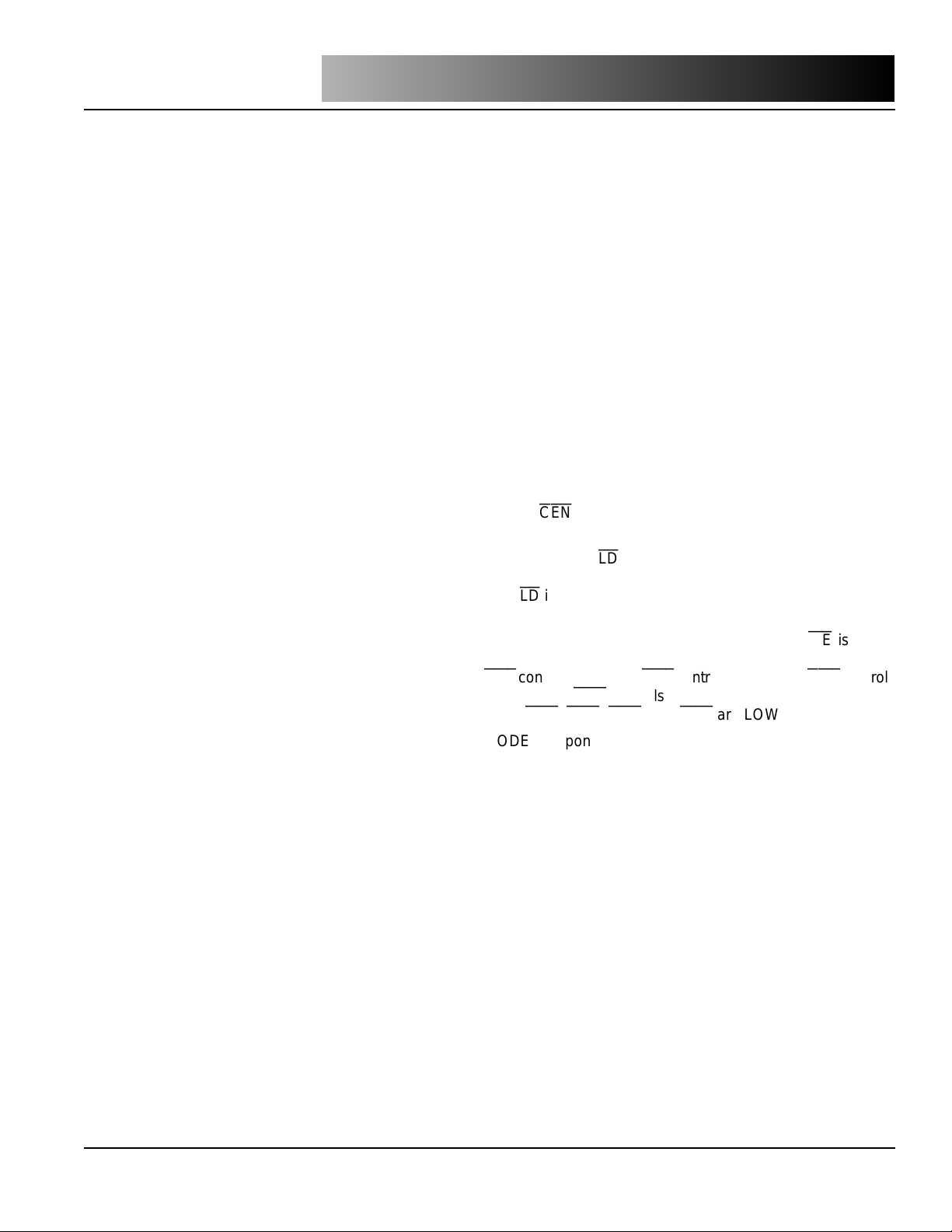
BLOCK DIAGRAM
MODE
A0-A15
CE1, CE2, CE3
64K x 32 BIT
MEMORY ARRAY
I
O
ADDRESS
R/W
CEN
ADV/LD
BW1
BW2
BW3
BW4
OE
I
O
INPUT REGISTER
O
I
CONTROL
CONTROL LOGIC
D
IN
MUX
D
OUT
SEL
I
CLOCK
OUTPUT
REGISTER
O
OE
2
GATE
DATA
I/O1-I/O32
DS
(Optional)
Integrated Silicon Solution, Inc.
ADVANCE INFORMATION SR050-0B
07/15/98
IS61NW6432
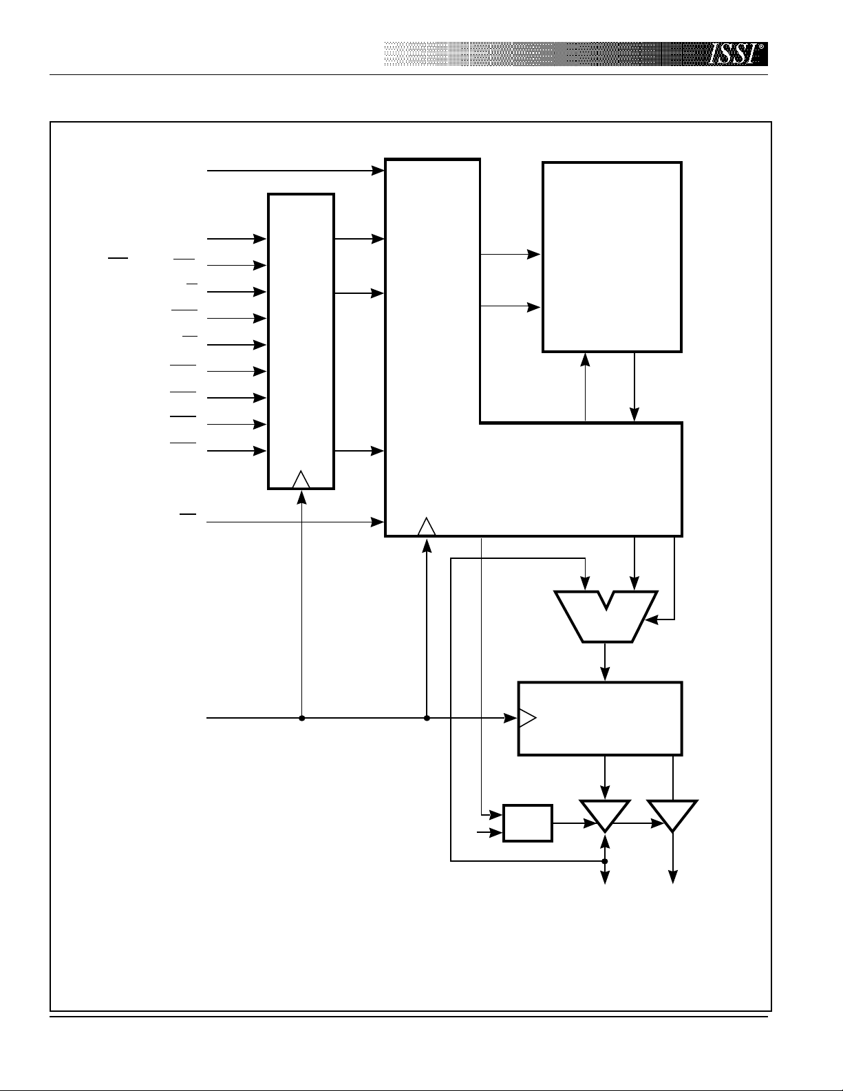
PIN CONFIGURATION
100-Pin TQFP and PQFP (Top View)
A6A7CE1
CE2
BW4
BW3
BW2
BW1
99 98 97 96 95 94 93 92 91 90 89 88 87 86 85 84 83 82 81
100
1
NC
NC
2
3
4
5
6
7
8
9
10
11
12
13
14
15
16
17
18
19
20
21
22
23
24
25
26
27
28
29
30
31 32 33 34 35 36 37 38 39 40 41 42 43 44 45
I/O17
I/O18
VCCQ
GNDQ
I/O19
I/O20
I/O21
I/O22
GNDQ
VCCQ
I/O23
I/O24
VCC
VCC
VCC
GND
I/O25
I/O26
VCCQ
GNDQ
I/O27
I/O28
I/O29
I/O30
GNDQ
VCCQ
I/O31
I/O32
CE3
VCC
GND
CLK
R/W
CENOEADV/LDNCNCA8A9
46 47 48 49 50
80
NC
79
I/O16
78
I/O15
77
VCCQ
76
GNDQ
75
I/O14
74
I/O13
73
I/O12
72
I/O11
71
GNDQ
70
VCCQ
69
I/O10
68
I/O9
67
GND
66
VCC
65
VCC
64
GND
63
I/O8
62
I/O7
61
VCCQ
60
GNDQ
59
I/O6
58
I/O5
57
I/O4
56
I/O3
55
GNDQ
54
VCCQ
53
I/O2
52
I/O1
51
NC
A5A4A3A2A1
MODE
PIN DESCRIPTIONS
A0-A15 Address Inputs
CLK Clock
CEN
ADV/
CD
BW1-BW4
R/
W
CE1
, CE2,
CE3
OE
Note:
1. Optional, NC or DS.
Integrated Silicon Solution, Inc.
ADVANCE INFORMATION SR050-0B
07/15/98
Clock Enable
Advance Load
Synchronous Byte Write Enable
Read/Write
Synchronous Chip Enable
Output Enable
A0
NC
NC
GND
VCC
NC
NC
A13
DS
A14
(1)
A15
NC
Data Strobe
A10
A11
A12
I/O1-I/O32 Data Input/Output
MODE Burst Sequence Mode
VCC +3.3V Power Supply
GND Ground
VCCQ Isolated Output Buffer Supply: +3.3V
GNDQ Isolated Output Buffer Ground
NC No Connect
3
IS61NW6432
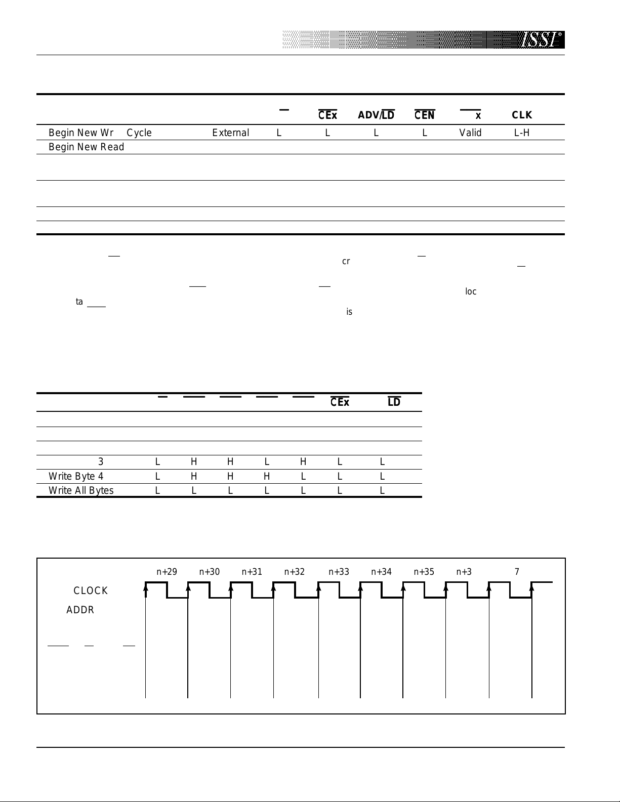
TRUTH TABLE
(1)
Address
Operation Used R/
WW
W
WW
CExCEx
CEx
CExCEx
ADV/
LDLD
LD
LDLD
CENCEN
CEN
CENCEN
BWxBWx
BWx
BWxBWx
Begin New Write Cycle External LLLLValid L-H
Begin New Read Cycle External H L L L X L-H
Advance Burst Counter
(2)
Internal X X H L Valid L-H
(Burst Write)
Advance Burst Counter Internal X X H L X L-H
(Burst Read)
Deselect (2 Cycle)
Hold/NOOP
Notes:
1. "X" Means don't care.
2. When ADV/LD signal is sampled HIGH, the internal burst counter is incremented. The R/W signal is ignored when the
counter is advanced. Therefore, the nature of the burst cycle (Read or Write) is determined by the status of the R/W signal
when the first address is loaded at the beginning of the burst cycle.
3. Deselect cycle is initiated when
tri-state two cycles after deselect is initiated.
4. When
CEN
The state of all the internal registers remains unchanged.
(3)
(4)
CEx
is sampled high at the rising edge of clock, that clock edge is blocked from propogating through the part.
X X H L L X L-H
XXXXHXL-H
is sampled HIGH and ADV/LD sampled LOW at rising edge of clock. The data bus will
CLK
PARTIAL TRUTH TABLE (Non-burst)
Function R/
W
WW
BW1BW1
BW1
BW1BW1
BW2BW2
BW2
BW2BW2
BW3BW3
BW3
BW3BW3
BW4BW4
BW4
BW4BW4
CExCEx
CEx
CExCEx
ADV/
WW
Read H XXXXL L
Write Byte 1 L L H H H L L
Write Byte 2 L H L H H L L
Write Byte 3 L H H L H L L
Write Byte 4 L H H H L L L
Write All Bytes LLLLLL L
FUNCTIONAL TIMING DIAGRAM
CYCLE
CLOCK
ADDRESS
(A0-A15)
CONTROL
(BWx, R/W, ADV/LD)
n+29 n+30 n+31 n+32 n+33 n+34 n+35 n+36 n+37
A29 A30 A31 A32 A33 A34 A35 A36 A37
C29 C30 C31 C32 C33 C34 C35 C36 C37
LDLD
LD
LDLD
4
DATA
(I/O1-I/O32)
D27 D28 D29 D30 D31 D32 D33 D34 D35
Integrated Silicon Solution, Inc.
ADVANCE INFORMATION SR050-0B
07/15/98

IS61NW6432
TYPICAL OPERATION (
Cycle Address R/
CE1, CE3
WW
W
WW
and
ADV/
CEN
are LOW, CE2 is HIGH, Non-Burst Operation)
LDLD
LD
LDLD
CExCEx
CEx
CExCEx
CENCEN
CEN
CENCEN
n A0 H L L L X ? D–2 ?
n+1 A1 L L LLL?D–1 ?
n+2 A2 H L L L X L D0 Data Out
n+3 A3 L L L L L X D1 Data In
n+4 A4 H L L L X L D2 Data Out
n+5 A5 L L L L L X D3 Data In
n+6 A6 H L L L X L D4 Data Out
n+7 A7 L L L L L X D5 Data In
n+8 A8 H L L L X L D6 Data Out
n+9 A9 L L L L L X D7 Data In
n+10 A10 H L L L X L D8 Data Out
n+11 A11 H L L L X X D9 Data In
n+12 A12 L L LLLLD10 Data Out
n+13 A13 L L LLLLD11 Data Out
n+14 A14 H L L L X X D12 Data In
n+15 A15 H L L L X X D13 Data In
n+16 A16 H L L L X L D14 Data Out
n+17 A17 L L LLLLD15 Data Out
n+18 A18 L L LLLLD16 Data Out
n+19 A19 L L L L L X D17 Data In
n+20 A20 H L L L X X D18 Data In
n+21 A21 H L L L X X D19 Data In
Note:
1. H = High; L = Low; X = Don't Care; ? = Don't Know; Z = High Impedance
BWxBWx
BWx
BWxBWx
OEOE
OE
OEOE
I/O Comments
Integrated Silicon Solution, Inc.
ADVANCE INFORMATION SR050-0B
07/15/98
5

IS61NW6432
READ OPERATION
Cycle Address R/
n A0 H L L L X X X Address and Control meet setup
n+1 X X X L L X X X Clock Setup Valid
n+2 X X X X X X L D0 Contents of Address A0 Read Out
WW
W
WW
ADV/
LDLD
LD
LDLD
CExCEx
CEx
CExCEx
CENCEN
CEN
CENCEN
BWxBWx
BWx
BWxBWx
OEOE
OE
I/O Comments
OEOE
BURST READ OPERATION
Cycle Address R/
n A0 H L L L X X X Address and Control meet setup
n+1 X X H X L X X X Clock Setup Valid, Advance Counter
n+2 X X H X L X L D0 Address A0 Read Out, Inc. Count
n+3 X X H X L X L D0+1 Address A0+1 Read Out, Inc. Count
n+4 X X H X L X L D0+2 Address A0+2 Read Out, Inc. Count
n+5 A1 H L L L X L D0+3 Address A0+3 Read Out, Load A1
n+6 X X H X L X L D0 Address A0 Read Out, Inc. Count
n+7 X X H X L X L D1 Address A1 Read Out, Inc. Count
n+8 A2 H L L L X L D1+1 Address A1+1 Read Out, Load A2
WW
W
WW
ADV/
LDLD
LD
LDLD
CExCEx
CEx
CExCEx
CENCEN
CEN
CENCEN
BWxBWx
BWx
BWxBWx
OEOE
OE
I/O Comments
OEOE
WRITE OPERATION
Cycle Address R/
n A0 L L L L L X X Address and Control meet setup
n+1 X X X L L X X X Clock Setup Valid
n+2 X X X X L X X D0 Write D0 to Address A0
WW
W
WW
ADV/LD
CExCEx
CEx
CExCEx
CENCEN
CEN
CENCEN
BWxBWx
BWx
BWxBWx
OEOE
OE
I/O Comments
OEOE
BURST WRITE OPERATION
Cycle Address R/
n A0 L L L L L X X Address and Control meet setup
n+1 X X H X L L X X Clock Setup Valid, Inc. Count
n+2 X X H X L L X D0 Address A0 Write, Inc. Count
n+3 X H H L L X X D0+1 Address A0+1 Write, Inc. Count
n+4 X X H X L L X D0+2 Address A0+2 Write, Inc. Count
n+5 A1 L L L L L X D0+3 Address A0+3 Write, Load A1
n+6 X X H X L L X D0 Address A0 Write, Inc. Count
n+7 X X H X L L X D1 Address A1 Write, Inc. Count
n+8 A2 L L L L L X D1+1 Address A1+1 Write, Load A2
Note:
1. H = High; L = Low; X = Don't Care; ? = Don't Know; Z = High Impedance
WW
W
WW
ADV/
LDLD
LD
LDLD
CExCEx
CEx
CExCEx
CENCEN
CEN
CENCEN
BWxBWx
BWx
BWxBWx
OEOE
OE
I/O Comments
OEOE
6
Integrated Silicon Solution, Inc.
ADVANCE INFORMATION SR050-0B
07/15/98

IS61NW6432
READ OPERATION WITH CLOCK ENABLE USED
Cycle Address R/
n A0 H L L L X X X Address and Control meet setup
n+1 X X X X H X X X Clock n+1 Ignored
n+2 A1 H L L L X X X Clock Valid
n+3 X X X X H X L D0 Clock Ignored. Data D0 is on the bus
n+4 X X X X H X L D0 Clock Ignored. Data D0 is on the bus
n+5 A2 H L L L X L D0 Address A0 Read Out (bus trans.)
n+6 A3 ? L L L X L D1 Address A1 Read Out (bus trans.)
n+7 A4 ? L L L X L D2 Address A2 Read Out (bus trans.)
WW
W
WW
ADV/
LDLD
LD
LDLD
CExCEx
CEx
CExCEx
CENCEN
CEN
CENCEN
BWxBWx
BWx
BWxBWx
OEOE
OE
I/O Comments
OEOE
WRITE OPERATION WITH CLOCK ENABLE USED
Cycle Address R/
n A0 L L L L L X X Address and Control meet setup
n+1 X X X X H X X X Clock n+1 Ignored
n+2 A1 L L L L L X X Clock Valid
n+3 X X X X H X L di Clock Ignored.
n+4 X X X X H X L di Clock Ignored.
n+5 A2 L L L L L L D0 Write data D0 (bus trans.)
n+6 A3 ? L L L L L D1 Write data D1 (bus trans.)
n+7 A4 ? L L L L L D2 Write data D2 (bus trans.)
Note:
1. H = High; L = Low; X = Don't Care; ? = Don't Know; Z = High Impedance; di could be D0 if desired.
WW
W
WW
ADV/
LDLD
LD
LDLD
CExCEx
CEx
CExCEx
CENCEN
CEN
CENCEN
BWxBWx
BWx
BWxBWx
OEOE
OE
I/O Comments
OEOE
Integrated Silicon Solution, Inc.
ADVANCE INFORMATION SR050-0B
07/15/98
7

IS61NW6432
INTERLEAVED BURST ADDRESS TABLE (MODE = VCCQ or No Connect)
External Address 1st Burst Address 2nd Burst Address 3rd Burst Address
A1 A0 A1 A0 A1 A0 A1 A0
00 01 10 11
01 00 11 10
10 11 00 01
11 10 01 00
LINEAR BURST ADDRESS TABLE (MODE = GNDQ)
0,0
0,1A1', A0' = 1,1
1,0
ABSOLUTE MAXIMUM RATINGS
Symbol Parameter Value Unit
TBIAS Temperature Under Bias –10 to +85 °C
TSTG Storage Temperature –55 to +150 °C
PD Power Dissipation 1.8 W
IOUT Output Current (per I/O) 100 mA
VIN, VOUT Voltage Relative to GND for I/O Pins –0.5 to VCCQ + 0.3 V
VIN Voltage Relative to GND for –0.5 to 5.5 V
for Address and Control Inputs
Notes:
1. Stress greater than those listed under ABSOLUTE MAXIMUM RATINGS may cause
permanent damage to the device. This is a stress rating only and functional operation
of the device at these or any other conditions above those indicated in the operational
sections of this specification is not implied. Exposure to absolute maximum rating
conditions for extended periods may affect reliability.
2. This device contains circuity to protect the inputs against damage due to high static
voltages or electric fields; however, precautions may be taken to avoid application of
any voltage higher than maximum rated voltages to this high-impedance circuit.
3. This device contains circuitry that will ensure the output devices are in High-Z at power
up.
(1)
8
Integrated Silicon Solution, Inc.
ADVANCE INFORMATION SR050-0B
07/15/98

IS61NW6432
OPERATING RANGE
Range Ambient Temperature VCC
Commercial 0°C to +70°C 3.3V +10%, –5%
DC ELECTRICAL CHARACTERISTICS
(1)
(Over Operating Range)
Symbol Parameter Test Conditions Min. Max. Unit
VOH Output HIGH Voltage IOH = –5.0 mA 2.4 — V
VOL Output LOW Voltage IOL = 5.0 mA — 0.4 V
VIH Input HIGH Voltage 2.0 VCCQ + 0.3 V
VIL Input LOW Voltage –0.3 0.8 V
ILI Input Leakage Current GND ≤ VIN ≤ VCCQ
(2)
Com. –5 5 µA
ILO Output Leakage Current GND ≤ VOUT ≤ VCCQ, OE = VIH Com. –5 5 µA
POWER SUPPLY CHARACTERISTICS (Over Operating Range)
-5 -6 -7 -8
Symbol Parameter Test Conditions Min. Max. Min. Max. Min. Max. Min. Max. Unit
ICC AC Operating Device Selected, Com. — 230 — 220 — 210 — 200 mA
Supply Current All Inputs = VIL or VIH
OE
= VIH, Cycle Time ≥ tKC min.
ISB Standby Current Device Deselected, Com. — 60 — 60 — 60 — 60 mA
VCC = Max.,
All Inputs = VIH or VIL
CLK Cycle Time ≥ tKC min.,
CEN
= VIH
Notes:
1. MODE pin has an internal pull up. This pin may be a No Connect, tied to GND, or tied to V
2. MODE pin should be tied to Vcc or GND. It exhibits ±30 µA maximum leakage current when
tied to ≤ GND + 0.2V or ≥ Vcc – 0.2V.
CCQ.
Integrated Silicon Solution, Inc.
ADVANCE INFORMATION SR050-0B
07/15/98
9

IS61NW6432
CAPACITANCE
(1,2)
Symbol Parameter Conditions Max. Unit
CIN Input Capacitance VIN = 0V 6 pF
COUT Input/Output Capacitance VOUT = 0V 8 pF
Notes:
1. Tested initially and after any design or process changes that may affect these parameters.
2. Test conditions: T
A = 25°C, f = 1 MHz, Vcc = 3.3V.
AC TEST CONDITIONS
Parameter Unit
Input Pulse Level 0V to 3.0V
Input Rise and Fall Times 1.5 ns
Input and Output Timing 1.5V
and Reference Level
Output Load See Figures 1 and 2
AC TEST LOADS
3.3V
317 Ω
Output
Buffer
O
= 50Ω
Z
Figure 1
30 pF
1.5V
50Ω
OUTPUT
5 pF
Including
jig and
scope
Figure 2
351 Ω
10
Integrated Silicon Solution, Inc.
ADVANCE INFORMATION SR050-0B
07/15/98

IS61NW6432
READ/WRITE CYCLE SWITCHING CHARACTERISTICS
(1)
(Over Operating Range)
-5 -6 -7 -8
Symbol Parameter Min. Max. Min. Max. Min. Max. Min. Max. Unit
fmax Clock Frequency — 100 — 83 — 75 — 66 MHz
tKC Cycle Time 10 — 12 — 13 — 15 — ns
tKH Clock High Time 4 — 4 — 6 — 6 — ns
tKL Clock Low Time 4 — 4 — 6 — 6 — ns
tKQ Clock Access Time — 5 — 6 — 7 — 8 ns
(2)
tKQX
tKQLZ
tKQHZ
Clock High to Output Invalid 1.5 — 1.5 — 1.5 — 1.5 — ns
(2,3)
Clock High to Output Low-Z 2.0 — 2.0 — 2.0 — 2.0 — ns
(2,3)
Clock High to Output High-Z 1.5 3.5 2 3.5 2 3.5 2 3.5 ns
tOEQ Output Enable to Output Valid — 5 — 6 — 6 — 6 ns
(2)
tOEQX
tOELZ
tOEHZ
Output Disable to Output Invalid 0 — 0 — 0 — 0 — ns
(2,3)
Output Enable to Output Low-Z 0 — 0 — 0 — 0 — ns
(2,3)
Output Disable to Output High-Z — 3.5 — 3.5 — 3.5 — 3.5 ns
tAS Address Setup Time 2.0 — 2.0 — 2.0 — 2.0 — ns
tWS Read/Write Setup Time 2.0 — 2.0 — 2.0 — 2.0 — ns
tCES Chip Enable Setup Time 2.0 — 2.0 — 2.0 — 2.0 — ns
tSE Clock Enable Setup Time 2.0 — 2.0 — 2.0 — 2.0 — ns
tAVS Address Advance Setup Time 2.0 — 2.0 — 2.0 — 2.0 — ns
tAH Address Hold Time 0.5 — 0.5 — 0.5 — 0.5 — ns
tHE Clock EnableHold Time 0.5 — 0.5 — 0.5 — 0.5 — ns
tWH Write Hold Time 0.5 — 0.5 — 0.5 — 0.5 — ns
tCEH Chip Enable Hold Time 0.5 — 0.5 — 0.5 — 0.5 — ns
tALS Advance/Load (ADV/LD) Setup Time 2.0 — 2.0 — 2.0 — 2.0 — ns
tALH Advance/Load (ADV/LD) Hold Time 0.5 — 0.5 — 0.5 — 0.5 — ns
tds Data Setup Time 2.0 — 2.0 — 2.0 — 2.0 — ns
tdh Data Hold Time 0.5 — 0.5 — 0.5 — 0.5 — ns
tzq I/O From Tri-State to Valid 1.5 2.5 1.5 2.5 1.5 2.5 1.5 2.5 ns
Notes:
1. Configuration signal MODE is static and must not change during normal operation.
2. Guaranteed but not 100% tested. This parameter is periodically sampled.
3. Tested with load in Figure 2.
Integrated Silicon Solution, Inc.
ADVANCE INFORMATION SR050-0B
07/15/98
11

IS61NW6432
READ/WRITE CYCLE TIMING
tKC
CLK
tSE tHE
CEN
tALS tALH
ADV/LD
tAS
A15-A0
R/W
BW4-BW1
tCES tCEH
CE1
tCES tCEH
CE2
tCES tCEH
CE3
tAH
RD1
tWS tWH
RD2 RD3
tOEQ
tKLtKH
WR1
tWS tWH
WR1
RD4
tAVS
RD5
Unselected with CE3
tOEHZ
OE
DATAOUT
DATA
STROBE
DATA
IN
High-Z
High-Z
High-Z
tOELZ
1a 2a
tZQ
tKQLZ
tKQ
3a
tKQX
tDS tDH
Single Read Single Write
tOEQX
High-Z
1a
tKQ
4a 4b 4c 4d
Burst Read
tKQX
tKQHZ
High-Z
Unselected
12
Integrated Silicon Solution, Inc.
ADVANCE INFORMATION SR050-0B
07/15/98

IS61NW6432
ORDERING INFORMATION
Commercial Range: 0°C to +70°C
Speed (ns) Order Part Number Package
5 IS61NW6432-5TQ TQFP
IS61NW6432-5PQ PQFP
6 IS61NW6432-6TQ TQFP
IS61NW6432-6PQ PQFP
7 IS61NW6432-7TQ TQFP
IS61NW6432-7PQ PQFP
8 IS61NW6432-8TQ TQFP
IS61NW6432-8PQ PQFP
NOTICE
Integrated Silicon Solution, Inc., reserves the right to make changes to the products contained in this publication in order to
improve design, performance or reliability. Integrated Silicon Solution, Inc. assumes no responsibility for the use of any
circuits described herein, conveys no license under any patent or other right, and makes no representation that the circuits
are free of patent infringement. Charts and schedules contained herein reflect representative operating parameters, and may
vary depending upon a user's specific application. While the information in this publication has been carefully checked,
Integrated Silicon Solution, Inc. shall not be liable for any damages arising as a result of any error or omission.
Integrated Silicon Solution, Inc. does not recommend the use of any of its products in life support applications where the failure
or malfunction of the product can reasonably be expected to cause failure of the life support system or to significantly affect
its safety or effectiveness. Products are not authorized for use in such applications unless Integrated Silicon Solution, Inc.
receives written assurances, to its satisfaction, that: (a) the risk of injury or damage has been minimized; (b) the user assumes
all such risks; and (c) potential liability of Integrated Silicon Solution, Inc. is adequately protected under the circumstances.
Copyright 1998 Integrated Silicon Solution, Inc.
Reproduction in whole or in part, without the prior written consent of Integrated Silicon Solution, Inc., is prohibited.
ISSI
Integrated Silicon Solution, Inc.
2231 Lawson Lane
Santa Clara, CA 95054
Tel: 1-800-379-4774
Fax: (408) 588-0806
e-mail: sales@issi.com
http://www.issi.com
®
Integrated Silicon Solution, Inc.
ADVANCE INFORMATION SR050-0B
07/15/98
13
 Loading...