

Datasheet IS61LV6464-7TQ, IS61LV6464-7PQI, IS61LV6464-6TQI, IS61LV6464-6TQ, IS61LV6464-6PQ Datasheet (ISSI)
...Page 1

IS61LV6464 ISSI
®
Integrated Silicon Solution, Inc. — 1-800-379-4774
1
Rev. A
04/17/01
ISSI reserves the right to make changes to its products at any time without notice in order to improve design and supply the best possible product. We assume no responsibility for any
errors which may appear in this publication. © Copyright 2001, Integrated Silicon Solution, Inc.
FEATURES
• Fast access time:
– -100 MHz; 6 ns-83 MHz;
7 ns-75 MHz; 8 ns-66 MHz
• Internal self-timed write cycle
• Individual Byte Write Control and Global Write
• Clock controlled, registered address, data and
control
• Pentium™ or linear burst sequence control
using MODE input
• Five chip enables for simple depth expansion
and address pipelining
• Common data inputs and data outputs
• Power-down control by ZZ input
• JEDEC 128-Pin TQFP 14mm x 20mm
package
• Single +3.3V power supply
• 2.5V V
CCQ (I/O supply)
• Control pins mode upon power-up:
– MODE in interleave burst mode
– ZZ in normal operation mode
These control pins can be connected to GND
Q
or VCCQ to alter their power-up state
DESCRIPTION
The ISSI IS61LV6464 is a high-speed, low-power synchronous static RAM designed to provide a burstable, highperformance, secondary cache for the Pentium™, 680X0™,
and PowerPC™ microprocessors. It is organized as 65,536
words by 64 bits, fabricated with ISSI's advanced CMOS
technology. The device integrates a 2-bit burst counter, highspeed SRAM core, and high-drive capability outputs into a
single monolithic circuit. All synchronous inputs pass through
registers controlled by a positive-edge-triggered single clock
input.
Write cycles are internally self-timed and are initiated by the
rising edge of the clock input. Write cycles can be from one to
eight bytes wide as controlled by the write control inputs.
Separate byte enables allow individual bytes to be written.
BW1 controls I/O1-I/O8, BW2 controls I/O9-I/O16, BW3 controls I/O17-I/O24, BW4 controls I/O25-I/O32, BW5 controls
I/O33-I/O40, BW6 controls I/O41-I/O48, BW7 controls I/O49I/O56, BW8 controls I/O57-I/O64, conditioned by BWE being
LOW. A LOW on GW input would cause all bytes to be written.
Bursts can be initiated with either ADSP (Address Status
Processor) or ADSC (Address Status Cache Controller) input
pins. Subsequent burst addresses can be generated internally by the IS61LV6464 and controlled by the ADV (burst
address advance) input pin.
Asynchronous signals include output enable (OE), sleep mode
input (ZZ), and burst mode input (MODE). A HIGH input on the
ZZ pin puts the SRAM in the power-down state. When ZZ is
pulled LOW (or no connect), the SRAM normally operates
after the wake-up period. A LOW input, i.e., GND
Q, on MODE
pin selects LINEAR Burst. A VCCQ (or no connect) on MODE
pin selects INTERLEAVED Burst.
64K x 64 SYNCHRONOUS
PIPELINE STATIC RAM
APRIL 2001
Page 2
IS61LV6464 ISSI
®
2
Integrated Silicon Solution, Inc. — 1-800-379-4774
Rev. A
04/17/01
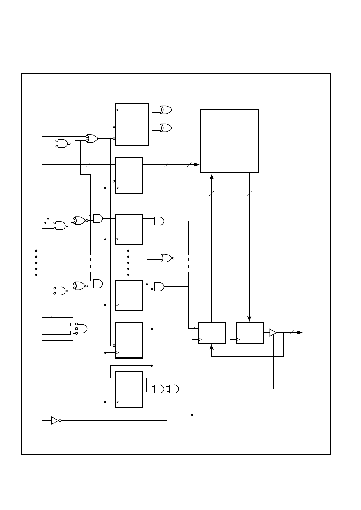
BLOCK DIAGRAM
16
BINARY
COUNTER
A15-A0
BW1
GW
CLR
CE
CLK
Q0
Q1
MODE
A0'
A0
A1
A1'
CLK
ADV
ADSC
ADSP
14 16
ADDRESS
REGISTER
CE
D
CLK
Q
DQ57-DQ64
BYTE WRITE
REGISTERS
D
CLK
Q
DQ8-DQ1
BYTE WRITE
REGISTERS
D
CLK
Q
ENABLE
REGISTER
CE
D
CLK
Q
ENABLE
DELAY
REGISTER
D
CLK
Q
BWE
BW8
CE
CE2
CE2
CE3
CE3
64K x 64
MEMORY
ARRAY
64
INPUT
REGISTERS
CLK
OUTPUT
REGISTERS
CLK
64
OE
8
64
OE
DATA[64:1]
Page 3
IS61LV6464 ISSI
®
Integrated Silicon Solution, Inc. — 1-800-379-4774
3
Rev. A
04/17/01
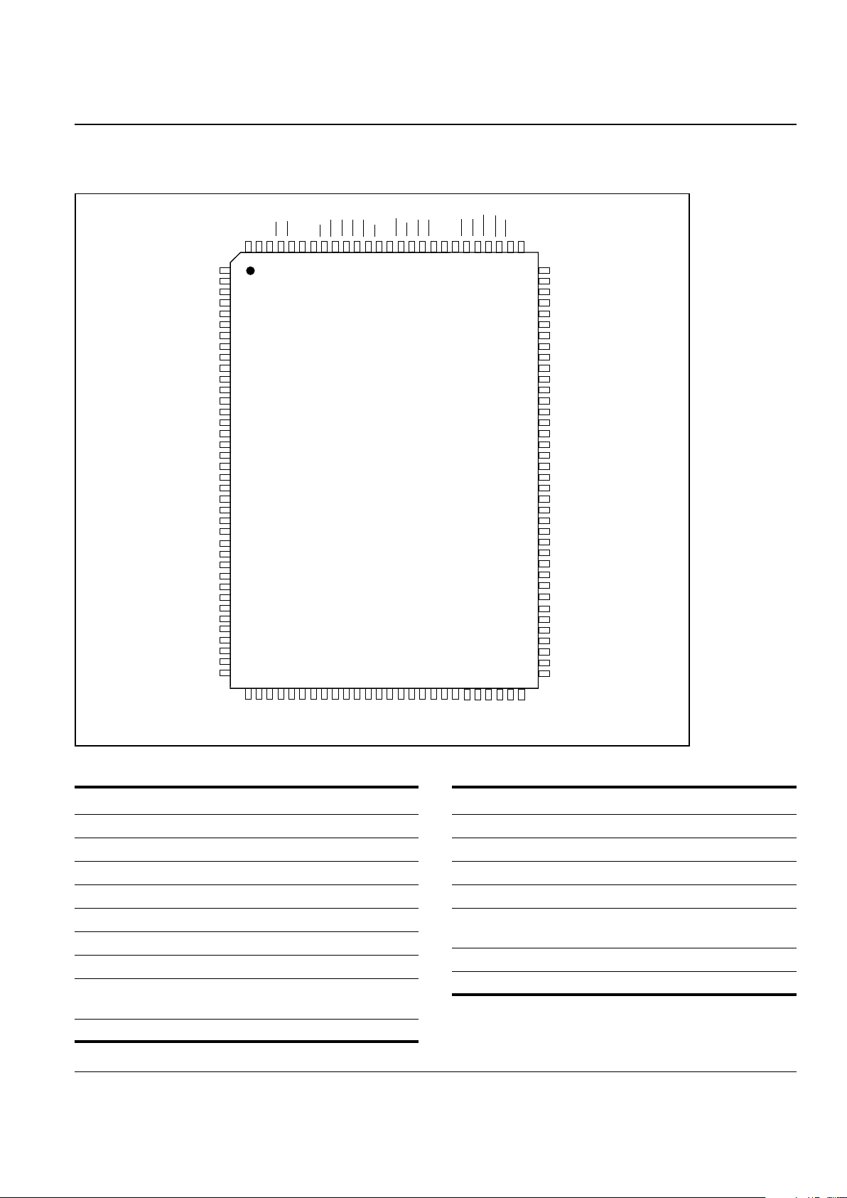
PIN CONFIGURATION
128-Pin TQFP
VCCQ
I/O
32
I/O
31
I/O
30
I/O
29
I/O
28
I/O
27
I/O
26
I/O
25
I/O
24
I/O
23
I/O
22
GNDQ
VCCQ
I/O
21
I/O
20
I/O
19
I/O
18
I/O
17
I/O
16
I/O
15
I/O
14
I/O
13
I/O
12
GNDQ
VCCQ
I/O
11
I/O
10
I/O
9
I/O
8
I/O
7
I/O
6
I/O
5
I/O
4
I/O
3
I/O
2
I/O
1
GNDQ
VCCQ
CE3
CE2
CE3
CE2
GND
VCCCEBW8
BW7
BW6
BW5OECLK
BWEGWBW4
BW3
GND
VCC
BW2
BW1
ADSC
ADSP
ADV
GNDQ
GNDQ
I/O
33
I/O
34
I/O
35
I/O
36
I/O
37
I/O
38
I/O
39
I/O
40
I/O
41
I/O
42
I/O
43
VCCQ
GNDQ
I/O
44
I/O
45
I/O
46
I/O
47
I/O
48
I/O
49
I/O
50
I/O
51
I/O
52
I/O
53
VCCQ
GNDQ
I/O
54
I/O
55
I/O
56
I/O
57
I/O
58
I/O
59
I/O
60
I/O
61
I/O
62
I/O
63
I/O
64
VCCQ
1
2
3
4
5
6
7
8
9
10
11
12
13
14
15
16
17
18
19
20
21
22
23
24
25
26
27
28
29
30
31
32
33
34
35
36
37
38
102
101
100
99
98
97
96
95
94
93
92
91
90
89
88
87
86
85
84
83
82
81
80
79
78
77
76
75
74
73
72
71
70
69
68
67
66
65
GNDQNCMODE
A15
A14
A13
VCC
GND
A12
A11
A10
A9
A8NCA7A6A5A4A3
VCC
GND
A2A1A0
ZZ
VCCQ
39404142434445464748495051525354555657585960616263
64
128
127
126
125
124
123
122
121
120
119
118
117
116
115
114
113
112
111
110
109
108
107
106
105
104
103
PIN DESCRIPTIONS
A0-A15 Address Inputs
CLK Clock
ADSP Processor Address Status
ADSC Controller Address Status
ADV Burst Address Advance
BW1-BW8 Synchronous Byte Write Enable
BWE Byte Write Enable
GW Global Write Enable
CE, CE2, CE2, Synchronous Chip Enable
CE3, CE3
OE Output Enable
DQ1-DQ64 Data Input/Output
ZZ Sleep Mode
MODE Burst Sequence Mode
VCC +3.3V Power Supply
GND Ground
VCCQ Isolated Output Buffer Supply:
+2.5V
NC No Connect
GNDQ Isolated Output Buffer Ground
Page 4

IS61LV6464 ISSI
®
4
Integrated Silicon Solution, Inc. — 1-800-379-4774
Rev. A
04/17/01
TRUTH TABLE
ADDRESS
OPERATION USED CE3 CE2 CE3 CE2 CE ADSP ADSC ADV WRITE OE CLK I/O
Deselected, Power-down None X X X X H X L X X X L-H High-Z
Deselected, Power-down None L X X X L L XXXXL-HHigh-Z
Deselected, Power-down None X L X X L L XXXXL-HHigh-Z
Deselected, Power-down None X X H X L L XXXXL-HHigh-Z
Deselected, Power-down None X X X H L L XXXXL-HHigh-Z
Deselected, Power-down None L X X X L H L X X X L-H High-Z
Deselected, Power-down None X L X X L H L X X X L-H High-Z
Deselected, Power-down None X X H X L H L X X X L-H High-Z
Deselected, Power-down None X X X H L H L X X X L-H High-Z
Read Cycle, Begin Burst External H H L L L L X X X L L-H Dout
Read Cycle, Begin Burst External H H L L L L X X X H L-H High-Z
Write Cycle, Begin Burst External H H L L L H L X L X L-H Din
Read Cycle, Begin Burst External H H L L L H L X H L L-H Dout
Read Cycle, Begin Burst External H H L L L H L X H H L-H High-Z
Read Cycle, Continue Burst Next X X X X X H H L H L L-H Dout
Read Cycle, Continue Burst Next X X X X X H H L H H L-H High-Z
Read Cycle, Continue Burst Next X X X X H X H L H L L-H Dout
Read Cycle, Continue Burst Next X X X X H X H L H H L-H High-Z
Write Cycle, Continue Burst Next X X X X X H H L L X L-H Din
Write Cycle, Continue Burst Next X X X X H X H L L X L-H Din
Read Cycle, Suspend Burst Current X X X X X HHHHLL-HDout
Read Cycle, Suspend Burst Current X X X X X HHHHHL-HHigh-Z
Read Cycle, Suspend Burst Current X X X X H X H H H L L-H Dout
Read Cycle, Suspend Burst Current X X X X H X HHHHL-HHigh-Z
Write Cycle, Suspend Burst Current X X X X X H H H L X L-H Din
Write Cycle, Suspend Burst Current X X X X H X H H L X L-H Din
Notes:
1. All inputs except OE must meet setup and hold times for the Low-to-High transition of clock (CLK).
2. Wait states are inserted by suspending burst.
3. X means don't care. WRITE=L means any one or more byte write enable signals (BW1-BW8) and BWE are LOW or GW is LOW.
WRITE=H means all byte write enable signals are HIGH.
4. For a Write operation following a Read operation, OE must be HIGH before the input data required setup time and held HIGH
throughout the input data hold time.
5. ADSP LOW always initiates an internal READ at the Low-to-High edge of clock. A WRITE is performed by setting one or more
byte write enable signals and BWE LOW or GW LOW for the subsequent L-H edge of clock.
Page 5

IS61LV6464 ISSI
®
Integrated Silicon Solution, Inc. — 1-800-379-4774
5
Rev. A
04/17/01
ASYNCHRONOUS TRUTH TABLE
Operation ZZ OE I/O STATUS
Pipelined Read L L Dout
Pipelined Read L H High-Z
Write L L High-Z
Write L H Din
Deselect L X High-Z
Sleep H X High-Z
WRITE TRUTH TABLE
Operation GW BWE BW8 BW7 BW6 BW5 BW4 BW3 BW2 BW1
Read HHXX XXXXXX
Read H LHH HHHHHH
Write all bytes H L L L L L L L L L
Write all bytes L X X X X X X X X X
Write Byte 1 H L H H H H H H H L
Write Byte 2 H L H H H H H H L H
Write Byte 3 H L H H H H H L H H
Write Byte 4 H L H H H H L H H H
Write Byte 5 H L H H H L H H H H
Write Byte 6 H L H H L H H H H H
Write Byte 7 H L H L H H H H H H
Write Byte 8 H L L H H H H H H H
Page 6
IS61LV6464 ISSI
®
6
Integrated Silicon Solution, Inc. — 1-800-379-4774
Rev. A
04/17/01
INTERLEAVED BURST ADDRESS TABLE (MODE = VCC or No Connect)
External Address 1st Burst Address 2nd Burst Address 3rd Burst Address
A1 A0 A1 A0 A1 A0 A1 A0
00 01 10 11
01 00 11 10
10 11 00 01
11 10 01 00
LINEAR BURST ADDRESS TABLE (MODE = GNDQ)
0,0
1,0
0,1A1’, A0’ = 1,1
ABSOLUTE MAXIMUM RATINGS
(1)
Symbol Parameter Value Unit
TBIAS Temperature Under Bias –10 to +85 °C
TSTG Storage Temperature –55 to +150 °C
PD Power Dissipation 1.0 W
IOUT Output Current (per I/O) 100 mA
VIN, VOUT Voltage Relative to GND for I/O Pins –0.5 to VCCQ + 0.3 V
VIN Voltage Relative to GND for –0.5 to 5.5 V
for Address and Control Inputs
VCC Voltage on Vcc Supply Relatiive to GND –0.5 to 4.6 V
Notes:
1. Stress greater than those listed under ABSOLUTE MAXIMUM RATINGS may cause
permanent damage to the device. This is a stress rating only and functional operation of the
device at these or any other conditions above those indicated in the operational sections of
this specification is not implied. Exposure to absolute maximum rating conditions for extended
periods may affect reliability.
2. This device contains circuity to protect the inputs against damage due to high static voltages
or electric fields; however, precautions may be taken to avoid application of any voltage higher
than maximum rated voltages to this high-impedance circuit.
3. This device contains circuitry that will ensure the output devices are in High-Z at power up.
Page 7

IS61LV6464 ISSI
®
Integrated Silicon Solution, Inc. — 1-800-379-4774
7
Rev. A
04/17/01
OPERATING RANGE
Range Ambient Temperature VCC VCCQ
Commercial 0°C to +70°C 3.3V +10%, –5% 2.375V min., 3.465V max.
Industrial –40°C to +85°C 3.3V +10%, –5% 2.375V min., 3.465V max.
DC ELECTRICAL CHARACTERISTICS
(1)
(Over Operating Range)
Symbol Parameter Test Conditions Min. Max. Unit
VOH Output HIGH Voltage IOH = –1.0 mA 2.0 — V
VOL Output LOW Voltage IOL = 1 mA — 0.4 V
VIH Input HIGH Voltage 1.7 VCCQ + 0.3 V
VIL Input LOW Voltage –0.3 0.8 V
I
LI Input Leakage Current GND - VIN - VCCQ
(2)
Com. –22µA
Ind. –10 10
ILO Output Leakage Current GND - VOUT - VCCQ, OE = VIH Com. –22µA
Ind. –10 10
POWER SUPPLY CHARACTERISTICS (Over Operating Range)
-100 -6-7-8
Symbol Parameter Test Conditions
Typ. Max. Typ. Max. Typ. Max. Typ. Max. Uni
t
ICC AC Operating Device Selected, Com. 210 250 190 200 160 170 140 150 mA
Supply Current All Inputs = VIL or VIH Ind. —— 200 220 170 190 160 170 mA
OE = VIH,
Cycle Time • tKC min.
ISB1 Standby Current Device Deselected, Com. 45 70 45 70 45 70 45 70 mA
TTL Inputs VCC = Max., Ind. —— 50 75 50 75 50 75 mA
All Inputs = VIH or VIL
CLK Cycle Time • tKC min.
ISB2 Standby Current Device Deselected, Com. 2 5 2 5 2 5 2 5 mA
CMOS Inputs VCC = Max., Ind. —— 510 510 510mA
VIN = VCC • 0.2V, or VIN - 0.2V
CLK Cycle Time • tKC min.
IZZ Power-Down Mode ZZ = VCCQ, CLK Running Com. 1 5 1 5 1 5 1 5 mA
Current All Inputs - GND + 0.2V Ind. —— 215 215 215mA
or • VCC – 0.2V
Note:
1. The MODE pin has an internal pullup. ZZ pin has an internal pull-down. This pin may be a No Connect, tied to GND, or tied to
VCCQ.
2. The MODE pin should be tied to Vcc or GND. It exhibits ±10 µA maximum leakage current when tied to - GND + 0.2V
or • Vcc – 0.2V.
Page 8

IS61LV6464 ISSI
®
8
Integrated Silicon Solution, Inc. — 1-800-379-4774
Rev. A
04/17/01
CAPACITANCE
(1,2)
Symbol Parameter Conditions Max. Unit
CIN Input Capacitance VIN = 0V 5 pF
COUT Input/Output Capacitance VOUT = 0V 7 pF
Notes:
1. Tested initially and after any design or process changes that may affect these parameters.
2. Test conditions: T
A = 25°C, f = 1 MHz, Vcc = 3.3V.
AC TEST CONDITIONS
Parameter Unit
Input Pulse Level for Input Pins 0V to 3.0V
Input Pulse Level for I/O Pins 0V to 2.5V
Input Rise and Fall Times 1.5 ns
Input and Output Timing 1.25V
and Reference Level
Output Load See Figures 1 and 2
AC TEST LOADS
Figure 2
317 Ω
5 pF
Including
jig and
scope
351 Ω
OUTPUT
2.5V
Figure 1
Output
Buffer
Z
O
= 50Ω
1.25V
50Ω
30 pF
Page 9

IS61LV6464 ISSI
®
Integrated Silicon Solution, Inc. — 1-800-379-4774
9
Rev. A
04/17/01
READ CYCLE SWITCHING CHARACTERISTICS (Over Operating Range)
-100 -6 -7 -8
Symbol Parameter Min. Max. Min. Max. Min. Max. Min. Max. Unit
tKC Cycle Time 10 — 12 — 13 — 15 — ns
tKH Clock High Time 4 — 4.5 — 5 — 6 — ns
tKL Clock Low Time 4 — 4.5 — 5 — 6 — ns
tKQ Clock Access Time — 5 — 6 — 7 — 8ns
tKQX
(1)
Clock High to Output Invalid 2.5 — 2.5 — 3 — 3 — ns
tKQLZ
(1,2)
Clock High to Output Low-Z 0 — 0 — 0 — 0 — ns
tKQHZ
(1,2)
Clock High to Output High-Z 2 5 2 5 2 5 2 6 ns
tOEQ Output Enable to Output Valid — 5 — 5 — 5 — 5ns
tOEQX
(1)
Output Disable to Output Invalid 0 — 0 — 0 — 0 — ns
tOELZ
(1,2)
Output Enable to Output Low-Z 0 — 0 — 0 — 0 — ns
tOEHZ
(1,2)
Output Disable to Output High-Z 2 5 2 5 2 5 2 6 ns
tAS Address Setup Time 2.5 — 2.5 — 2.5 — 2.5 — ns
tSS Address Status Setup Time 2.5 — 2.5 — 2.5 — 2.5 — ns
tWS Write Setup Time 2.5 — 2.5 — 2.5 — 2.5 — ns
tCES Chip Enable Setup Time 2.5 — 2.5 — 2.5 — 2.5 — ns
tAVS Address Advance Setup Time 2.5 — 2.5 — 2.5 — 2.5 — ns
tAH Address Hold Time 0.5 — 0.5 — 0.5 — 0.5 — ns
tSH Address Status Hold Time 0.5 — 0.5 — 0.5 — 0.5 — ns
tWH Write Hold Time 0.5 — 0.5 — 0.5 — 0.5 — ns
tCEH Chip Enable Hold Time 0.5 — 0.5 — 0.5 — 0.5 — ns
tAVH Address Advance Hold Time 0.5 — 0.5 — 0.5 — 0.5 — ns
Note:
1. Guaranteed but not 100% tested. This parameter is periodically sampled.
2. Tested with load in Figure 2.
Page 10

IS61LV6464 ISSI
®
10
Integrated Silicon Solution, Inc. — 1-800-379-4774
Rev. A
04/17/01
READ CYCLE TIMING
Single Read
High-Z
High-Z
DATAOUT
DATAIN
OE
CE2, CE3
CE2, CE3
CE
BW8-BW1
BWE
GW
A15-A0
ADV
ADSC
ADSP
CLK
RD1 RD2
1a
2c 2d 3a
Unselected
Burst Read
tKQX
tKC
tKLtKH
tSS tSH
tSS tSH
tAS tAH
tWS tWH
tWS tWH
RD3
tCES tCEH
tCES tCEH
tCES tCEH
CE3, CE2 and CE2, CE3 only sampled with ADSP or ADSC
CE Masks ADSP
Unselected with CE2, CE3
tOEQ
tOEQX
tOELZ
tKQLZ
tKQ
tOEHZ
tKQHZ
ADSC initiate read
ADSP is blocked by CE inactive
tAVH
tAVS
Suspend Burst
Pipelined Read
2a 2b
Page 11

IS61LV6464 ISSI
®
Integrated Silicon Solution, Inc. — 1-800-379-4774
11
Rev. A
04/17/01
WRITE CYCLE SWITCHING CHARACTERISTICS (Over Operating Range)
-100 -6 -7 -8
Symbol Parameter Min. Max. Min. Max. Min. Max. Min. Max. Unit
tKC Cycle Time 10 — 12 — 13 — 15 — ns
tKH Clock High Time 4 — 4.5 — 5 — 6 — ns
tKL Clock Low Time 4 — 4.5 — 5 — 6 — ns
tAS Address Setup Time 2.5 — 2.5 — 2.5 — 2.5 — ns
tSS Address Status Setup Time 2.5 — 2.5 — 2.5 — 2.5 — ns
tWS Write Setup Time 2.5 — 2.5 — 2.5 — 2.5 — ns
tDS Data In Setup Time 2.5 — 2.5 — 2.5 — 2.5 — ns
tCES Chip Enable Setup Time 2.5 — 2.5 — 2.5 — 2.5 — ns
tAVS Address Advance Setup Time 2.5 — 2.5 — 2.5 — 2.5 — ns
tAH Address Hold Time 0.5 — 0.5 — 0.5 — 0.5 — ns
tSH Address Status Hold Time 0.5 — 0.5 — 0.5 — 0.5 — ns
tDH Data In Hold Time 0.5 — 0.5 — 0.5 — 0.5 — ns
tWH Write Hold Time 0.5 — 0.5 — 0.5 — 0.5 — ns
tCEH Chip Enable Hold Time 0.5 — 0.5 — 0.5 — 0.5 — ns
tAVH Address Advance Hold Time 0.5 — 0.5 — 0.5 — 0.5 — ns
Page 12

IS61LV6464 ISSI
®
12
Integrated Silicon Solution, Inc. — 1-800-379-4774
Rev. A
04/17/01
WRITE CYCLE TIMING
Single Write
DATA
OUT
DATA
IN
OE
CE2, CE3
CE2, CE3
CE
BW8-BW1
BWE
GW
A15-A0
ADV
ADSC
ADSP
CLK
WR1 WR2
Unselected
Burst Write
t
KC
t
KL
t
KH
t
SS
t
SH
t
AS
t
AH
t
WS
t
WH
t
WS
t
WH
WR3
t
CES
t
CEH
t
CES
t
CEH
t
CES
t
CEH
CE3, CE2 and CE2, CE3 only sampled with ADSP or ADSC
CE Masks ADSP
Unselected with CE2, CE3
ADSC initiate Write
ADSP is blocked by CE inactive
t
AVH
t
AVS
ADV must be inactive for ADSP Write
WR1 WR2
t
WS
t
WH
WR3
t
WS
t
WH
High-Z
High-Z
1a
3a
t
DS
t
DH
BW8-BW1 only are applied to first cycle of WR2
Write
2c 2d2b2a
Page 13

IS61LV6464 ISSI
®
Integrated Silicon Solution, Inc. — 1-800-379-4774
13
Rev. A
04/17/01
READ/WRITE CYCLE SWITCHING CHARACTERISTICS (Over Operating Range)
-100 -6 -7 -8
Symbol Parameter Min. Max. Min. Max. Min. Max. Min. Max. Unit
tKC Cycle Time 10 — 12 — 13 — 15 — ns
tKH Clock High Time 4 — 4.5 — 5 — 6 — ns
tKL Clock Low Time 4 — 4.5 — 5 — 6 — ns
tKQ Clock Access Time — 5 — 6 — 7 — 8ns
tKQX
(1)
Clock High to Output Invalid 2.5 — 2.5 — 3 — 3 — ns
tKQLZ
(1,2)
Clock High to Output Low-Z 0 — 0 — 0 — 0 — ns
tKQHZ
(1,2)
Clock High to Output High-Z 2 5 2 5 2 5 2 6 ns
tOEQ Output Enable to Output Valid — 5 — 5 — 5 — 5ns
tOEQX
(1)
Output Disable to Output Invalid 0 — 0 — 0 — 0 — ns
tOELZ
(1,2)
Output Enable to Output Low-Z 0 — 0 — 0 — 0 — ns
tOEHZ
(1,2)
Output Disable to Output High-Z 2 5 2 5 2 5 2 6 ns
tAS Address Setup Time 2.5 — 2.5 — 2.5 — 2.5 — ns
tSS Address Status Setup Time 2.5 — 2.5 — 2.5 — 2.5 — ns
tWS Write Setup Time 2.5 — 2.5 — 2.5 — 2.5 — ns
tCES Chip Enable Setup Time 2.5 — 2.5 — 2.5 — 2.5 — ns
tAH Address Hold Time 0.5 — 0.5 — 0.5 — 0.5 — ns
tSH Address Status Hold Time 0.5 — 0.5 — 0.5 — 0.5 — ns
tWH Write Hold Time 0.5 — 0.5 — 0.5 — 0.5 — ns
tCEH Chip Enable Hold Time 0.5 — 0.5 — 0.5 — 0.5 — ns
Note:
1. Guaranteed but not 100% tested. This parameter is periodically sampled.
2. Tested with load in Figure 2.
Page 14

IS61LV6464 ISSI
®
14
Integrated Silicon Solution, Inc. — 1-800-379-4774
Rev. A
04/17/01
READ/WRITE CYCLE TIMING
Single Read
Single Write
High-Z
High-Z
DATA
OUT
DATA
IN
OE
CE2, CE3
CE2, CE3
CE
BW8-BW1
BWE
GW
A15-A0
ADV
ADSC
ADSP
CLK
RD1 WR1
WR1
1a
1a
2a 2b 2c 2d
Unselected
Burst Read
t
KQX
t
KC
t
KL
t
KH
t
SS
t
SH
ADSP is blocked by CE inactive
t
SS
t
SH
t
AS
t
AH
t
WS
t
WH
t
WS
t
WH
t
WS
t
WH
RD2 RD3
t
CES
t
CEH
t
CES
t
CEH
t
CES
t
CEH
CE2, CE3 and CE2, CE3 only sampled with ADSP or ADSC
CE Masks ADSP
Unselected with CE2, CE3
t
OEQ
t
OEQX
t
OELZ
t
KQLZ
t
KQ
t
OEHZ
t
KQX
t
KQHZ
t
DS
t
DH
t
KQHZ
Page 15

IS61LV6464 ISSI
®
Integrated Silicon Solution, Inc. — 1-800-379-4774
15
Rev. A
04/17/01
SNOOZE AND RECOVERY CYCLE SWITCHING CHARACTERISTICS (Over Operating Range)
-100 -6 -7 -8
Symbol Parameter Min. Max. Min. Max. Min. Max. Min. Max. Unit
tKC Cycle Time 10 — 12 — 13 — 15 — ns
tKH Clock High Time 4 — 4.5 — 5 — 6 — ns
tKL Clock Low Time 4 — 4.5 — 5 — 6 — ns
tKQ Clock Access Time — 5 — 6 — 7 — 8ns
tKQX
(3)
Clock High to Output Invalid 2.5 — 2.5 — 3 — 3 — ns
tKQLZ
(3,4)
Clock High to Output Low-Z 0 — 0 — 0 — 0 — ns
tKQHZ
(3,4)
Clock High to Output High-Z 2 5 2 5 2 5 2 6 ns
tOEQ Output Enable to Output Valid — 5 — 5 — 5 — 5ns
tOEQX
(3)
Output Disable to Output Invalid 0 — 0 — 0 — 0 — ns
tOELZ
(3,4)
Output Enable to Output Low-Z 0 — 0 — 0 — 0 — ns
tOEHZ
(3,4)
Output Disable to Output High-Z 2 5 2 5 2 5 2 6 ns
tAS Address Setup Time 2.5 — 2.5 — 2.5 — 2.5 — ns
tSS Address Status Setup Time 2.5 — 2.5 — 2.5 — 2.5 — ns
tCES Chip Enable Setup Time 2.5 — 2.5 — 2.5 — 2.5 — ns
tAH Address Hold Time 0.5 — 0.5 — 0.5 — 0.5 — ns
tSH Address Status Hold Time 0.5 — 0.5 — 0.5 — 0.5 — ns
tCEH Chip Enable Hold Time 0.5 — 0.5 — 0.5 — 0.5 — ns
tZZS ZZ Standby
(1)
2 — 2 — 2 — 2 — cyc
tZZREC ZZ Recovery
(2)
2 — 2 — 2 — 2 — cyc
Notes:
1. The assertion of ZZ allows the SRAM to enter a lower power state than when deselected within the time specified. Data
retention is guaranteed when ZZ is asserted and clock remains active.
2. ADSC and ADSP must not be asserted for at least 2 cyc after leaving ZZ state.
3. Guaranteed but not 100% tested. This parameter is periodically sampled.
4. Tested with load in Figure 2.
Page 16

IS61LV6464 ISSI
®
16
Integrated Silicon Solution, Inc. — 1-800-379-4774
Rev. A
04/17/01
SNOOZE AND RECOVERY CYCLE TIMING
Single Read
High-Z
High-Z
DATA
OUT
DATA
IN
OE
CE2, CE3
CE2, CE3
CE
BW8-BW1
BWE
GW
A15-A0
ADV
ADSC
ADSP
CLK
RD1
1a
Read
Snooze with Data Retention
t
KC
t
KL
t
KH
t
SS
t
SH
t
AS
t
AH
RD2
t
CES
t
CEH
t
CES
t
CEH
t
CES
t
CEH
t
OEQ
t
OEQX
t
OELZ
t
KQLZ
t
KQ
t
OEHZ
t
KQX
t
KQHZ
ZZ
t
ZZS
t
ZZREC
Page 17

IS61LV6464 ISSI
®
Integrated Silicon Solution, Inc. — 1-800-379-4774
17
Rev. A
04/17/01
ORDERING INFORMATION
Commercial Range: 0°C to +70°C
Speed (ns) Order Part Number Package
100 IS61LV6464-100TQ TQFP
100 IS61LV6464-100PQ PQFP
83 IS61LV6464-6TQ TQFP
83 IS61LV6464-6PQ PQFP
75 IS61LV6464-7TQ TQFP
75 IS61LV6464-7PQ PQFP
66 IS61LV6464-8TQ TQFP
66 IS61LV6464-8PQ PQFP
Industrial Range: –40°C to +85°C
Speed (ns) Order Part Number Package
83 IS61LV6464-6TQI TQFP
83 IS61LV6464-6PQI PQFP
75 IS61LV6464-7TQI TQFP
75 IS61LV6464-7PQI PQFP
66 IS61LV6464-8TQI TQFP
66 IS61LV6464-8PQI PQFP
ISSI
®
Integrated Silicon Solution, Inc.
2231 Lawson Lane
Santa Clara, CA 95054
Tel: 1-800-379-4774
Fax: (408) 588-0806
E-mail: sales@issi.com
www.issi.com
 Loading...