

Datasheet IS61LV12824-8TQ, IS61LV12824-12TQI, IS61LV12824-12TQ, IS61LV12824-12BI, IS61LV12824-10TQI Datasheet (ISSI)
...
IS61LV12824 ISSI
®
Integrated Silicon Solution, Inc. — 1-800-379-4774
1
Rev. B
04/17/01
ISSI reserves the right to make changes to its products at any time without notice in order to improve design and supply the best possible product. We assume no responsibility for any
errors which may appear in this publication. © Copyright 2001, Integrated Silicon Solution, Inc.
FEATURES
• High-speed access time: 8, 9, 10, 12 ns
• CMOS low power operation
— 756 mW (max.) operating @ 8 ns
— 36 mW (max.) standby @ 8 ns
• TTL compatible interface levels
• Single 3.3V power supply
• Fully static operation: no clock or refresh
required
• Three state outputs
• Available in 119-pin Plastic Ball Grid Array
(PBGA) and 100-pin TQFP packages.
• Industrial temperature available
DESCRIPTION
The ISSI IS61LV12824 is a high-speed, static RAM organized
as 131,072 words by 24 bits. It is fabricated using ISSI's highperformance CMOS technology. This highly reliable process
coupled with innovative circuit design techniques, yields access times as fast as 8 ns with low power consumption.
When CE1, CE2 are HIGH and CE2 is LOW (deselected), the
device assumes a standby mode at which the power dissipation can be reduced down with CMOS input levels.
Easy memory expansion is provided by using Chip Enable
and Output Enable inputs, CE1, CE2, CE2 and OE. The active
LOW Write Enable (WE) controls both writing and reading of
the memory.
The IS61LV12824 is packaged in the JEDEC standard
119-pin PBGA and 100-pin TQFP.
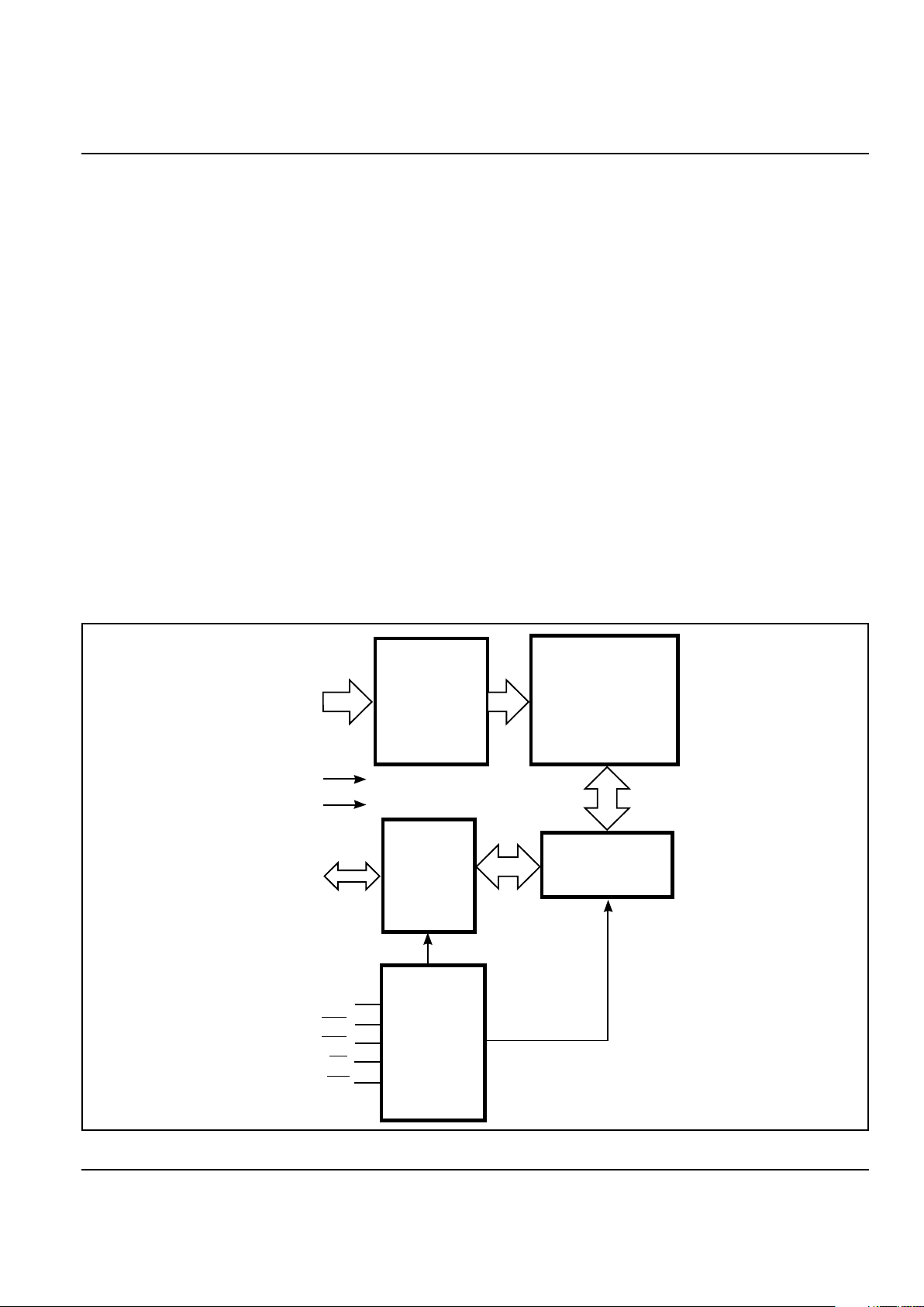
FUNCTIONAL BLOCK DIAGRAM
DECEMBER 1999
A0-A16
CE1
OE
WE
128K x 24
MEMORY ARRAY
DECODER
COLUMN I/O
CONTROL
CIRCUIT
GND
VCC
I/O
DATA
CIRCUIT
CE2
CE2
I/O0-I/O23
128K x 24 HIGH-SPEED CMOS STATIC RAM
WITH 3.3V SUPPLY
IS61LV12824
ISSI
®
2
Integrated Silicon Solution, Inc. — 1-800-379-4774
Rev. B
04/17/01
PIN CONFIGURATION - 119-pin PBGA
PIN DESCRIPTIONS
A0-A16 Address Inputs
I/O0-I/O23 Data Inputs/Outputs
CE1, CE2 Chip Enable Input LOW
CE2 Chip Enable Input HIGH
OE Output Enable Input
WE Write Enable Input
NC No Connection
Vcc Power
VCCQ I/O Power
GND Ground
1234567
A NC A11 A14 A15 A16 A4 NC
B NC A12 A13 CE1 A5 A3 NC
C I/O16 NC CE2 NC CE2 NC I/O0
D I/O17 VCCQ GND GND GND VCCQ I/O1
E I/O18 GND VCC GND VCC GND I/O2
F I/O19 VCCQ GND GND GND VCCQ I/O3
G I/O20 GND VCC GND VCC GND I/O4
H I/O21 VCCQ GND GND GND VCCQ I/O5
J VCCQ GND VCC GND VCC GND VCCQ
K I/O22 VCCQ GND GND GND VCCQ I/O6
L I/O23 GND VCC GND VCC GND I/O7
M I/O12 VCCQ GND GND GND VCCQ I/O8
N I/O13 GND VCC GND VCC GND I/O9
P I/O14 VCCQ GND GND GND VCCQ I/O10
R I/O15 NC NC NC NC NC I/O11
T NC A10 A8 WE A0 A1 NC
U NC A9 A7 OE A6 A2 NC
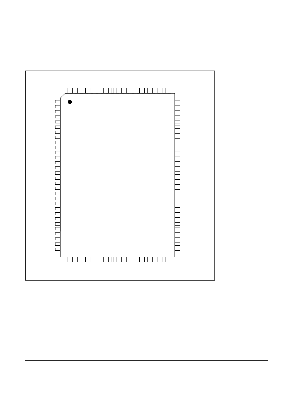
IS61LV12824
1
2
3
4
5
6
7
8
9
10
11
12
ISSI
®
Integrated Silicon Solution, Inc. — 1-800-379-4774
3
Rev. B
04/17/01
PIN CONFIGURATION
100-Pin TQFP
NC
Vcc
GND
I/O0
I/O1
GND
Vcc
Q
I/O2
I/O3
GND
Vcc
Q
I/O4
I/O5
Vcc
NC
NC
GND
I/O6
I/O7
Vcc
Q
GND
I/O8
I/O9
Vcc
Q
GND
I/O10
I/O11
Vcc
GND
NC
NCNCA11
A12
A13
A14
A15
CE2
Vcc
GND
CE2
CE1
A16A5A4A3NCNCNC
NC
NC
Vcc
GND
I/O16
I/O17
GND
Vcc
Q
I/O18
I/O19
GND
Vcc
Q
I/O20
I/O21
Vcc
NC
NC
GND
I/O22
I/O23
Vcc
Q
GND
I/O12
I/O13
Vcc
Q
GND
I/O14
I/O15
Vcc
GND
NC
1
2
3
4
5
6
7
8
9
10
11
12
13
14
15
16
17
18
19
20
21
22
23
24
25
26
27
28
29
30
80
79
78
77
76
75
74
73
72
71
70
69
68
67
66
65
64
63
62
61
60
59
58
57
56
55
54
53
52
51
100
99 98 97 96 95 94 93 92 91 90 89 88 87 86 85 84 83 82 81
31 32 33 34 35 36 37 38 39 40 41 42 43 44 45
NCNCNC
NC
A10
A9A8A7
OE
GND
Vcc
WE
A6A0A1
A2
NCNCNC
NC
46 47 48 49 50

IS61LV12824
ISSI
®
4
Integrated Silicon Solution, Inc. — 1-800-379-4774
Rev. B
04/17/01
OPERATING RANGE
Range Ambient Temperature VCC (8, 9 ns) VCC (10, 12 ns)
Commercial 0°C to +70°C 3.3V + 10%, – 5% 3.3V ± 10%
Industrial –40°C to +85°C 3.3V + 10%, – 5% 3.3V ± 10%
DC ELECTRICAL CHARACTERISTICS (Over Operating Range)
Symbol Parameter Test Conditions Min. Max. Unit
VOH Output HIGH Voltage VCC = Min., IOH = –4.0 mA 2.4 — V
VOL Output LOW Voltage VCC = Min., IOL = 8.0 mA — 0.4 V
VIH Input HIGH Voltage 2.2 VCC + 0.3 V
VIL Input LOW Voltage
(1)
–0.3 0.8 V
ILI Input Leakage GND ≤ VIN ≤ VCC –11µA
ILO Output Leakage GND ≤ VOUT ≤ VCC, Outputs Disabled –11µA
Note:
1. V
IL (min.) = –0.3V DC; VIL (min.) = –2.0V AC (pulse width ≤ 2.0 ns).
VIH (max.) = VCC + 0.3V DC; VIH (max.) = VCC + 2.0V AC (pulse width ≤ 2.0 ns).
ABSOLUTE MAXIMUM RATINGS
(1)
Symbol Parameter Value Unit
VCC Power Supply Voltage Relative to GND –0.5 to 5.0 V
VTERM Terminal Voltage with Respect to GND –0.5 to Vcc + 0.5 V
TSTG Storage Temperature –65 to + 150 °C
TBIAS Temperature Under Bias: Com. –10 to + 85 °C
Ind. –45 to + 90 °C
PT Power Dissipation 2.0 W
IOUT DC Output Current ±20 mA
Note:
1. Stress greater than those listed under ABSOLUTE MAXIMUM RATINGS may cause permanent
damage to the device. This is a stress rating only and functional operation of the device at these or
any other conditions above those indicated in the operational sections of this specification is not
implied. Exposure to absolute maximum rating conditions for extended periods may affect reliability.
TRUTH TABLE
Mode W E CE1 CE2 CE2 OE I/O0-I/O23 Vcc Current
Not Selected X H X X X High-Z ISB1, ISB2
XXLXX
XXXHX
Output Disabled H L H L H High-Z ICC
Read H L H L L DOUT ICC
Write L L H L X DIN ICC

IS61LV12824
1
2
3
4
5
6
7
8
9
10
11
12
ISSI
®
Integrated Silicon Solution, Inc. — 1-800-379-4774
5
Rev. B
04/17/01
CAPACITANCE
(1)
Symbol Parameter Conditions Max. Unit
CIN Input Capacitance VIN = 0V 6 pF
COUT Input/Output Capacitance VOUT = 0V 8 pF
Note:
1. Tested initially and after any design or process changes that may affect these parameters.
POWER SUPPLY CHARACTERISTICS
(1)
(Over Operating Range)
-8 ns -9 ns -10 ns -12 ns
Symbol Parameter Test Conditions Min. Max. Min. Max. Min. Max. Min. Max. Unit
ICC Vcc Dynamic Operating VCC = Max., Com. — 210 — 200 — 180 — 170 mA
Supply Current IOUT = 0 mA, f = fMAX Ind. —— —220 — 210 — 190
I
SB1 TTL Standby Current VCC = Max., Com. — 70 — 60 — 50 — 50 mA
(TTL Inputs) VIN = VIH or VIL, f = max. Ind. —— —70 — 55 — 55
CE1, CE2, ≥ VIH, CE2 ≤ VIL
ISB2 CMOS Standby VCC = Max., Com. — 10 — 10 — 10 — 10 mA
Current (CMOS Inputs) CE1, CE2 ≥ VCC – 0.2V, Ind. —— —20 — 20 — 20
CE2 ≤ 0.2V, VIN ≥ VCC – 0.2V,
or VIN ≤ 0.2V, f = 0
Note:
1. At f = f
MAX, address and data inputs are cycling at the maximum frequency, f = 0 means no input lines change.
AC TEST CONDITIONS
Parameter Unit
Input Pulse Level 0V to 3.0V
Input Rise and Fall Times 2 ns
Input and Output Timing 1.5V
and Reference Level
Output Load See Figures 1 and 2
AC TEST LOADS
Figure 1 Figure 2
319 Ω
5 pF
Including
jig and
scope
353 Ω
OUTPUT
3.3V
OUTPUT
Z
O
= 50Ω
1.5V
50Ω

IS61LV12824
ISSI
®
6
Integrated Silicon Solution, Inc. — 1-800-379-4774
Rev. B
04/17/01
READ CYCLE SWITCHING CHARACTERISTICS
(1)
(Over Operating Range)
-8 -9 -10 -12
Symbol Parameter Min. Max. Min. Max. Min. Max. Min. Max. Unit
tRC Read Cycle Time 8 — 9 — 10 — 12 — ns
tAA Address Access Time — 8 — 9 — 10 — 12 ns
tOHA Output Hold Time 3 — 3 — 3 — 3 — ns
tACE CE1, CE2 Access Time 8 ——9 — 10 — 12 ns
tACE2 CE2 Access Time
tDOE OE Access Time — 4 — 4 — 4 — 4ns
tHZOE
(2)
OE to High-Z Output 0 3 0 3 0 3 0 3 ns
tLZOE
(2)
OE to Low-Z Output 0 — 0 — 0 — 0 — ns
tHZCE
(2)
CE1, CE2 to High-Z Output 0 4 0 5 0 5 0 6 ns
tHZCE
2
(2)
CE2 to High-Z Output
tLZCE
(2)
CE, CE2 to Low-Z Output 3 — 3 — 3 — 3 — ns
tLZCE
2
(2)
CE2 to Low-Z Output
Notes:
1. Test conditions assume signal transition times of 2 ns or less, timing reference levels of 1.5V, input pulse levels of 0 to 3.0V and
output loading specified in Figure 1.
2. Tested with the load in Figure 2. Transition is measured ±200 mV from steady-state voltage. Not 100% tested.

IS61LV12824
1
2
3
4
5
6
7
8
9
10
11
12
ISSI
®
Integrated Silicon Solution, Inc. — 1-800-379-4774
7
Rev. B
04/17/01
READ CYCLE NO. 2
(1,3)
AC WAVEFORMS
READ CYCLE NO. 1
(1,2)
(Address Controlled) (CE1 = CE2 = OE = VIL; CE2 = VIH)
Notes:
1. WE is HIGH for a Read Cycle.
2. The device is continuously selected. OE, CE1, CE2 = V
IL. CE2 = VIH.
3. Address is valid prior to or coincident with CE1, CE2 LOW and CE2 HIGH transition.
DATA VALID
READ1.eps
PREVIOUS DATA VALID
t
AA
t
OHA
t
OHA
t
RC
D
OUT
ADDRESS
t
RC
t
OHA
t
AA
t
DOE
t
LZOE
t
ACS1
t
ACS2
t
LZCS1
t
LZCS2
t
HZOE
HIGH-Z
DATA VALID
ADDRESS
OE
CS1
CS2
D
OUT
t
HZCS1
t
HZCS2
CS2_RD2.eps

IS61LV12824
ISSI
®
8
Integrated Silicon Solution, Inc. — 1-800-379-4774
Rev. B
04/17/01
WRITE CYCLE SWITCHING CHARACTERISTICS
(1,3)
(Over Operating Range)
-8 -9 -10 -12
Symbol Parameter Min. Max. Min. Max. Min. Max. Min. Max. Unit
tWC Write Cycle Time 8 — 9 — 10 — 12 — ns
tSCE CE1, CE2 to Write End 7 — 8 — 8 — 9 — ns
tSCE
2
CE2 to Write End 7 — 8 — 8 — 9 —
tAW Address Setup Time 7 — 8 — 8 — 9 — ns
to Write End
tHA Address Hold from Write End 0 — 0 — 0 — 0 — ns
tSA Address Setup Time 0 — 0 — 0 — 0 — ns
tPWE1 WE Pulse Width (OE = HIGH) 6 — 8 — 8 — 9 — ns
tPWE2 WE Pulse Width (OE = LOW) 6 — 9 — 9 — 10 — ns
tSD Data Setup to Write End 4.5 — 5 — 5 — 5 — ns
tHD Data Hold from Write End 0 — 0 — 0 — 0 — ns
tHZWE
(2)
WE LOW to High-Z Output — 3.5 — 3.5 — 3.5 — 3.5 ns
tLZWE
(2)
WE HIGH to Low-Z Output 3 — 3 — 3 — 3 — ns
Notes:
1. Test conditions assume signal transition times of 2 ns or less, timing reference levels of 1.5V, input pulse levels of 0 to 3.0V
and output loading specified in Figure 1.
2. Tested with the load in Figure 2. Transition is measured ±200 mV from steady-state voltage. Not 100% tested.
3. The internal write time is defined by the overlap of CE1, CE2 LOW, CE2 HIGH and WE LOW. All signals must be in valid
states to initiate a Write, but any one can go inactive to terminate the Write. The Data Input Setup and Hold timing are
referenced to the rising or falling edge of the signal that terminates the write.

IS61LV12824
1
2
3
4
5
6
7
8
9
10
11
12
ISSI
®
Integrated Silicon Solution, Inc. — 1-800-379-4774
9
Rev. B
04/17/01
WRITE CYCLE NO. 1
(CE Controlled, OE = HIGH or LOW)
WRITE CYCLE NO. 2
(1)
(WE Controlled: OE = HIGH during Write Cycle)
DATA UNDEFINED
t
WC
VALID ADDRESS
t
SCE1
t
SCE2
t
PWE1
t
PWE2
t
AW
t
HA
HIGH-Z
t
HD
t
SA
t
HZWE
ADDRESS
CE1
CE2
WE
D
OUT
D
IN
DATAIN VALID
t
LZWE
t
SD
CE2_WR1.eps
DATA UNDEFINED
LOW
t
WC
VALID ADDRESS
t
PWE1
t
AW
t
HA
HIGH-Z
t
HD
t
SA
t
HZWE
ADDRESS
CE1
WE
D
OUT
D
IN
OE
DATAIN VALID
t
LZWE
t
SD
HIGH
CE2
CE2_WR2.eps

IS61LV12824
ISSI
®
10
Integrated Silicon Solution, Inc. — 1-800-379-4774
Rev. B
04/17/01
WRITE CYCLE NO. 3
(1)
(WE Controlled: OE I S LOW
DURING WRITE CYLE
)
Note:
1. The internal Write time is defined by the overlap of CE1 and CE2 = LOW, CE2 = HIGH and WE = LOW. All signals must be
in valid states to initiate a Write, but any can be deasserted to terminate the Write. The Data Input Setup and Hold timing is
referenced to the rising or falling edge of the signal that terminates the Write.
DATA UNDEFINED
t
WC
VALID ADDRESS
LOW
LOW
t
PWE2
t
AW
t
HA
HIGH-Z
t
HD
t
SA
t
HZWE
ADDRESS
CE1
WE
D
OUT
D
IN
OE
DATAIN VALID
t
LZWE
t
SD
HIGH
CE2
CE2_WR3.eps

IS61LV12824
1
2
3
4
5
6
7
8
9
10
11
12
ISSI
®
Integrated Silicon Solution, Inc. — 1-800-379-4774
11
Rev. B
04/17/01
ORDERING INFORMATION
Commercial Range: 0°C to +70°C
Speed (ns) Order Part No. Package
8 IS61LV12824-8B Plastic Ball Grid Array
IS61LV12824-8TQ TQFP
9 IS61LV12824-9B Plastic Ball Grid Array
IS61LV12824-9TQ TQFP
10 IS61LV12824-10B Plastic Ball Grid Array
IS61LV12824-10TQ TQFP
12 IS61LV12824-12B Plastic Ball Grid Array
IS61LV12824-12TQ TQFP
ORDERING INFORMATION
Industrial Range: –40°C to +85°C
Speed (ns) Order Part No. Package
9 IS61LV12824-9BI Plastic Ball Grid Array
IS61LV12824-9TQI TQFP
10 IS61LV12824-10BI Plastic Ball Grid Array
IS61LV12824-10TQI TQFP
12 IS61LV12824-12BI Plastic Ball Grid Array
IS61LV12824-12TQI TQFP
ISSI
®
Integrated Silicon Solution, Inc.
2231 Lawson Lane
Santa Clara, CA 95054
Tel: 1-800-379-4774
Fax: (408) 588-0806
E-mail: sales@issi.com
www.issi.com
 Loading...