

Datasheet IS61C64AH-25J, IS61C64AH-20U, IS61C64AH-20J, IS61C64AH-15U, IS61C64AH-25U Datasheet (ICSI)
...Page 1
IS61C64AH
8K x 8 HIGH-SPEED CMOS STATIC RAM
FEATURES
• High-speed access time: 15, 20, 25 ns
• Automatic power-down when chip is
deselected
• CMOS low power operation
— 450 mW (typical) operating
— 250 µW (typical) standby
• TTL compatible interface levels
• Single 5V power supply
• Fully static operation: no clock or refresh
required
• Three state outputs
• Two Chip Enables (CE1 and CE2) for
simple memory expansion
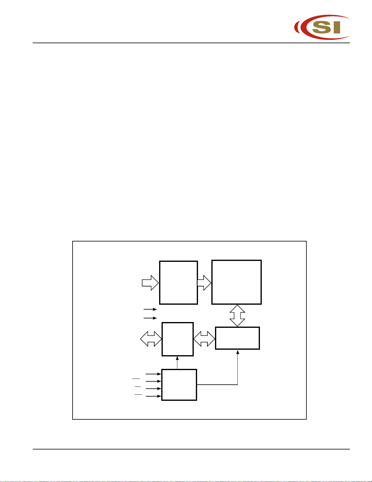
FUNCTIONAL BLOCK DIAGRAM
DESCRIPTION
The ICSI IS61C64AH is a very high-speed, low power,
8192-word by 8-bit static RAM. It is fabricated using ICSI's
high-performance CMOS technology. This highly reliable process coupled with innovative circuit design techniques, yields
access times as fast as 15 ns with low power consumption.
When CE1 is HIGH or CE2 is LOW (deselected), the device
assumes a standby mode at which the power dissipation can
be reduced down to 250 µW (typical) with CMOS input levels.
Easy memory expansion is provided by using two Chip Enable
inputs, CE1 and CE2. The active LOW Write Enable (WE)
controls both writing and reading of the memory.
The IS61C64AH is packaged in the JEDEC standard 28-pin,
300mil SOJ and 330mil SOP.
A0-A12
VCC
GND
I/O0-I/O7
CE2
CE1
OE
WE
ICSI reserves the right to make changes to its products at any time without notice in order to improve design and supply the best possible product. We assume no responsibility for any errors
which may appear in this publication. © Copyright 2000, Integrated Circuit Solution Inc.
DECODER
I/O
DATA
CIRCUIT
CONTROL
CIRCUIT
256 X 256
MEMORY ARRAY
COLUMN I/O
Integrated Circuit Solution Inc. 1
SR001-B
Page 2
IS61C64AH
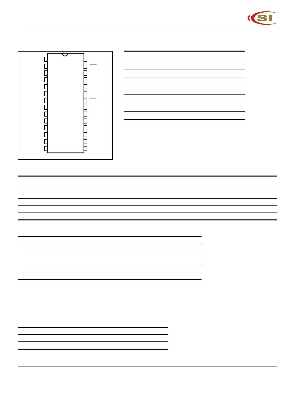
PIN CONFIGURATION
28-Pin SOJ and SOP
PIN DESCRIPTIONS
NC
A12
A7
A6
A5
A4
A3
A2
A1
A0
I/O0
I/O1
I/O2
GND
1
2
3
4
5
6
7
8
9
10
11
12
13
14
28
27
26
25
24
23
22
21
20
19
18
17
16
15
VCC
WE
CE2
A8
A9
A11
OE
A10
CE1
I/O7
I/O6
I/O5
I/O4
I/O3
A0-A12 Address Inputs
CE1 Chip Enable 1 Input
CE2 Chip Enable 2 Input
OE Output Enable Input
WE Write Enable Input
I/O0-I/O7 Input/Output
Vcc Power
GND Ground
TRUTH TABLE
Mode
WEWE
WE
WEWE
Not Selected X H X X High-Z ISB1, ISB2
(Power-down) X X L X High-Z ISB1, ISB2
Output Disabled H L H H High-Z ICC
Read H L H L DOUT ICC
Write L L H X DIN ICC
CE1CE1
CE1 CE2
CE1CE1
OEOE
OE I/O Operation Vcc Current
OEOE
ABSOLUTE MAXIMUM RATINGS
(1)
Symbol Parameter Value Unit
VTERM Terminal Voltage with Respect to GND –0.5 to +7.0 V
TBIAS Temperature Under Bias –55 to +125 °C
TSTG Storage Temperature –65 to +150 °C
PT Power Dissipation 1.0 W
IOUT DC Output Current (LOW) 20 mA
Notes:
1. Stress greater than those listed under ABSOLUTE MAXIMUM RATINGS may cause
permanent damage to the device. This is a stress rating only and functional operation of the
device at these or any other conditions above those indicated in the operational sections of
this specification is not implied. Exposure to absolute maximum rating conditions for
extended periods may affect reliability.
OPERATING RANGE
Range Ambient Temperature VCC
Commercial 0°C to +70°C 5V ± 10%
Industrial
Notes:
1. Industrial supplement specification available upon request.
2 Integrated Circuit Solution Inc.
(1)
–40°C to +85°C 5V ± 10%
SR001-B
Page 3
IS61C64AH
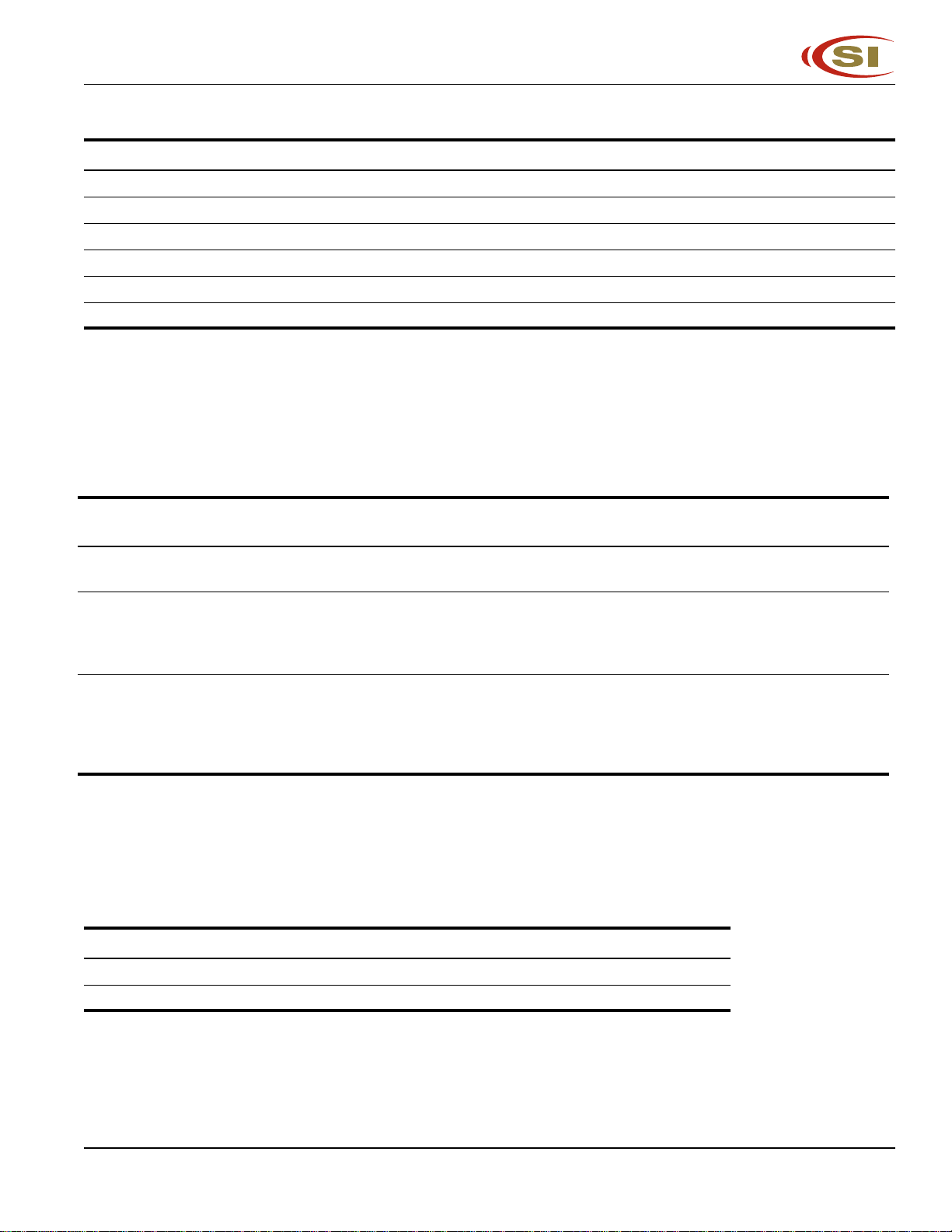
DC ELECTRICAL CHARACTERISTICS (Over Operating Range)
Symbol Parameter Test Conditions Min. Max. Unit
VOH Output HIGH Voltage VCC = Min., IOH = –4.0 mA 2.4 — V
VOL Output LOW Voltage VCC = Min., IOL = 8.0 mA — 0.4 V
VIH Input HIGH Voltage 2.2 VCC + 0.5 V
VIL Input LOW Voltage
ILI Input Leakage GND ≤ VIN ≤ VCC –2 2 µA
ILO Output Leakage GND ≤ VOUT ≤ VCC, Outputs Disabled –2 2 µA
Note:
1. VIL = –3.0V for pulse width less than 10 ns.
POWER SUPPLY CHARACTERISTICS
Symbol Parameter Test Conditions Min. Max. Min. Max. Min. Max. Unit
ICC Vcc Dynamic Operating VCC = Max., — 135 — 120 — 110 mA
Supply Current IOUT = 0 mA, f = fMAX
ISB1 TTL Standby Current VCC = Max., — 20 — 20 — 20 mA
(TTL Inputs) VIN = VIH or VIL
ISB2 CMOS Standby VCC = Max., — 6 — 6 — 6 mA
Current (CMOS Inputs) CE1 ≥ VCC – 0.2V,
(1)
(1)
CE1 ≥ VIH or
CE2 ≥ VIL, f = 0
CE2 ≤ 0.2V,
VIN ≥ VCC – 0.2V, or
VIN ≤ 0.2V, f = 0
–0.5 0.8 V
(Over Operating Range)
-15 ns -20 ns -25 ns
1
2
3
4
5
6
7
8
Note:
1. At f = f
CAPACITANCE
Notes:
1. Tested initially and after any design or process changes that may affect these parameters.
2. Test conditions: T
Integrated Circuit Solution Inc. 3
SR001-B
MAX, address and data inputs are cycling at the maximum frequency, f = 0 means no input lines change.
(1,2)
Symbol Parameter Conditions Max. Unit
CIN Input Capacitance VIN = 0V 5 pF
COUT Output Capacitance VOUT = 0V 7 pF
A = 25°C, f = 1 MHz, Vcc = 5.0V.
9
10
11
12
Page 4
IS61C64AH
READ CYCLE SWITCHING CHARACTERISTICS
(1)
(Over Operating Range)
-15 ns -20 ns -25 ns
Symbol Parameter Min. Max. Min. Max. Min. Max. Unit
tRC Read Cycle Time 15 — 20 — 25 — ns
tAA Address Access Time — 15 — 20 — 25 ns
tOHA Output Hold Time 3 — 3 — 3 — ns
tACE1 CE1 Access Time — 15 — 20 — 25 ns
tACE2 CE2 Access Time — 15 — 20 — 25 ns
tDOE OE Access Time — 7 — 7 — 9 ns
(2)
tLZOE
tHZOE
tLZCE1
tLZCE2
tHZCE
tPU
tPD
Notes:
1. Test conditions assume signal transition times of 5 ns or less, timing reference levels of 1.5V, input pulse levels of 0 to 3.0V
and output loading specified in Figure 1.
2. Tested with the load in Figure 2. Transition is measured ±500 mV from steady-state voltage. Not 100% tested.
3. Not 100% tested.
OE to Low-Z Output 0 — 0 — 0 — ns
(2)
OE to High-Z Output — 6 — 7 — 9 ns
(2)
CE1 to Low-Z Output 3 — 3 — 3 — ns
(2)
CE2 to Low-Z Output 3 — 3 — 3 — ns
(2)
CE1 or CE2 to High-Z Output — 8 — 10 — 12 ns
(3)
CE1 or CE2 to Power-Up 0 — 0 — 0 — ns
(3)
CE1 or CE2 to Power-Down — 15 — 20 — 20 ns
AC TEST CONDITIONS
Parameter Unit
Input Pulse Level 0V to 3.0V
Input Rise and Fall Times 3 ns
Input and Output Timing 1.5V
and Reference Level
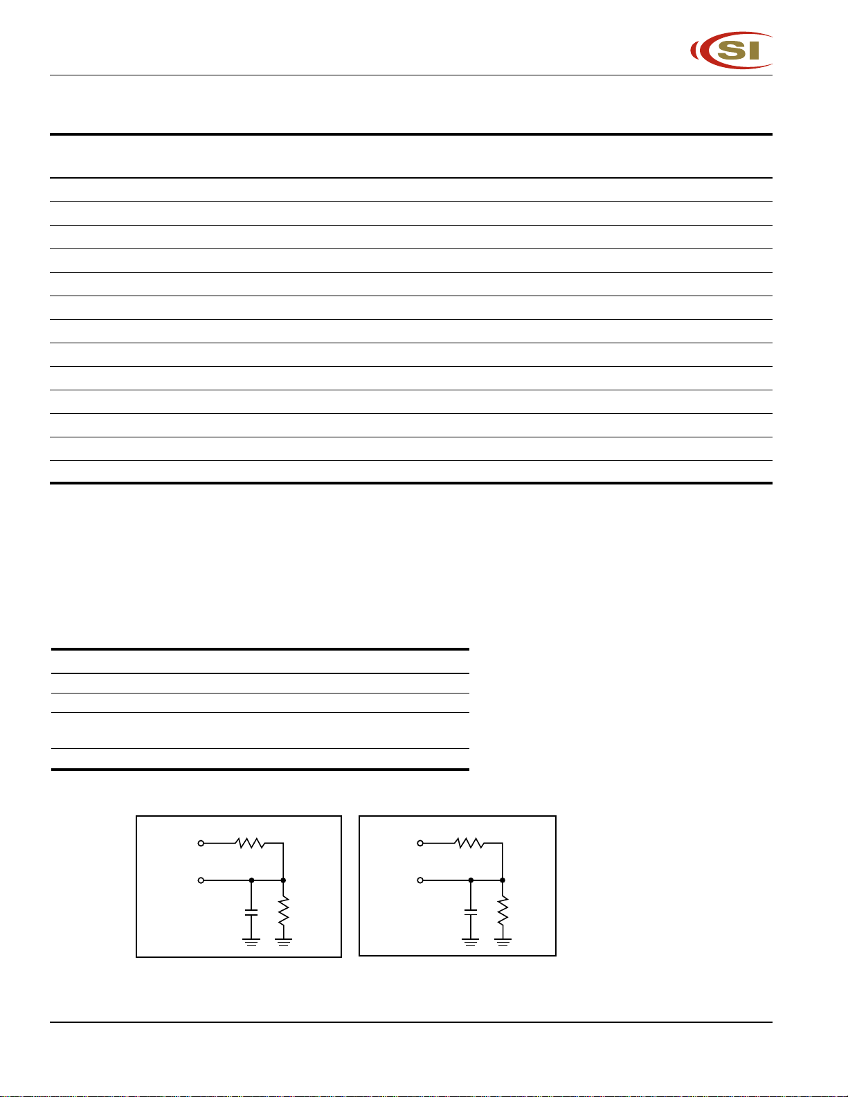
Output Load See Figures 1 and 2
AC TEST LOADS
480 Ω
5V
OUTPUT
30 pF
Including
jig and
scope
255 Ω
Figure 1. Figure 2.
OUTPUT
5V
5 pF
Including
jig and
scope
480 Ω
255 Ω
4 Integrated Circuit Solution Inc.
SR001-B
Page 5
IS61C64AH
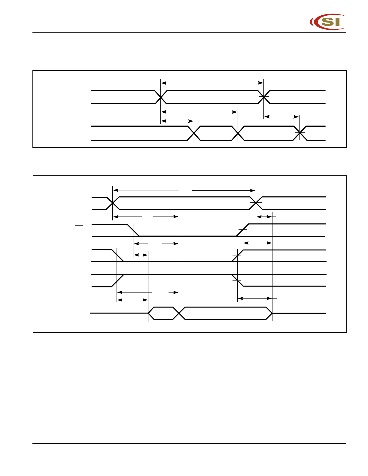
AC WAVEFORMS
READ CYCLE NO. 1
ADDRESS
D
OUT
READ CYCLE NO. 2
ADDRESS
OE
(1,2)
PREVIOUS DATA VALID
(1,3)
t
AA
t
OHA
1
t
RC
2
t
AA
DATA VALID
t
OHA
3
4
t
RC
5
t
OHA
6
t
DOE
t
CE1
CE2
t
LZCE1
t
LZCE2
D
OUT
Notes:
1. WE is HIGH for a Read Cycle.
2. The device is continuously selected. OE, CE1 = V
3. Address is valid prior to or coincident with CE1 LOW and CE2 HIGH transitions.
HIGH-Z
LZOE
t
ACE1
t
ACE2
IL, CE2 = VIH.
DATA VALID
t
HZOE
t
HZCE1
t
HZCE2
7
8
9
10
11
12
Integrated Circuit Solution Inc. 5
SR001-B
Page 6
IS61C64AH
WRITE CYCLE SWITCHING CHARACTERISTICS
(1,3)
(Over Operating Range)
-12 ns -15 ns -20 ns -25 ns
Symbol Parameter Min. Max. Min. Max. Min. Max. Min. Max. Unit
tWC Write Cycle Time 12 — 15 — 20 — 25 — ns
tSCE1 CE1 to Write End 10 — 12 — 17 — 22 — ns
tSCE2 CE2 to Write End 10 — 12 — 17 — 22 — ns
tAW Address Setup Time to Write End 10 — 12 — 15 — 20 — ns
tHA Address Hold from Write End 0 — 0 — 0 — 0 — ns
tSA Address Setup Time 0 — 0 — 0 — 0 — ns
(4)
tPWE
WE Pulse Width 8 — 10 — 12 — 15 — ns
tSD Data Setup to Write End 8 — 9 — 10 — 12 — ns
tHD Data Hold from Write End 0 — 0 — 0 — 0 — ns
(2)
tHZWE
tLZWE
Notes:
1. Test conditions assume signal transition times of 5 ns or less, timing reference levels of 1.5V, input pulse levels of 0 to 3.0V
and output loading specified in Figure 1.
2. Tested with the load in Figure 2. Transition is measured ±500 mV from steady-state voltage. Not 100% tested.
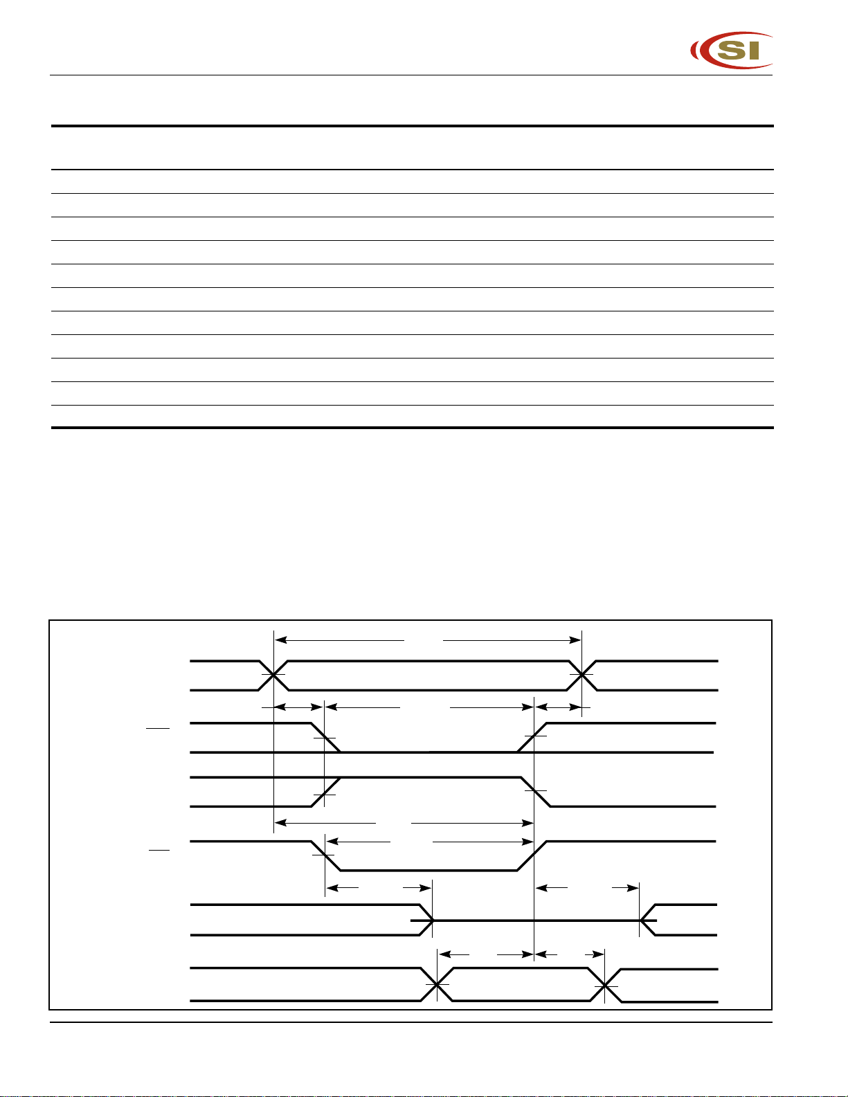
3. The internal write time is defined by the overlap of CE1 LOW, CE2 HIGH and WE LOW. All signals must be in valid states to
initiate a Write, but any one can go inactive to terminate the Write. The Data Input Setup and Hold timing are referenced to the
rising or falling edge of the signal that terminates the write.
WE LOW to High-Z Output — 6 — 8 — 10 — 12 ns
(2)
WE HIGH to Low-Z Output 0 — 0 — 0 — 0 — ns
AC WAVEFORMS
WRITE CYCLE NO. 1
ADDRESS
CE1
CE2
WE
D
OUT
DIN
(CE Controlled, OE is HIGH or LOW)
t
WC
VALID ADDRESS
t
t
SA
DATA UNDEFINED
t
HZWE
SCE1
t
SCE2
t
AW
t
PWE1
t
PWE2
(1 )
HIGH-Z
t
SD
DATAIN VALID
t
HA
t
LZWE
t
HD
6 Integrated Circuit Solution Inc.
SR001-B
Page 7
IS61C64AH
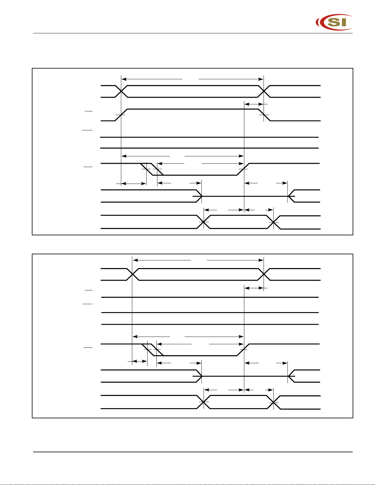
AC WAVEFORMS
WRITE CYCLE NO. 2
ADDRESS
OE
CE1
CE2
WE
OUT
D
D
IN
(OE is HIGH During Write Cycle)
VALID ADDRESS
LOW
HIGH
t
AW
t
t
SA
DATA UNDEFINED
HZWE
t
WC
t
PWE1
(1,2)
HIGH-Z
t
SD
DATAIN VALID
1
t
HA
2
3
4
t
LZWE
5
t
HD
6
WRITE CYCLE NO. 3
(OE is LOW During Write Cycle)
(1)
t WC
ADDRESS
OE
CE1
CE2
LOW
LOW
HIGH
VALID ADDRESS
t HA
t AW
t PWE2
WE
t SA
OUT
D
D
IN
Notes:
1. The internal write time is defined by the overlap of CE1 LOW, CE2 HIGH and WE LOW. All signals must be in valid states to
initiate a Write, but any one can go inactive to terminate the Write. The Data Input Setup and Hold timing are referenced to the
rising or falling edge of the signal that terminates the write.
2. I/O will assume the High-Z state if OE = V
DATA UNDEFINED
IH.
t HZWE
HIGH-Z
t SD
DATAIN VALID
t LZWE
t HD
7
8
9
10
11
12
Integrated Circuit Solution Inc. 7
SR001-B
Page 8
IS61C64AH
ORDERING INFORMATION
Commercial Range: 0°C to +70°C
Speed (ns) Order Part No. Package
15 IS61C64AH-15J 300mil SOJ
IS61C64AH-15U 330mil SOP
20 IS61C64AH-20J 300mil SOJ
IS61C64AH-20U 330mil SOP
25 IS61C64AH-25J 300mil SOJ
IS61C64AH-25U 330mil SOP
Integrated Circuit Solution Inc.
HEADQUARTER:
NO.2, TECHNOLOGY RD. V, SCIENCE-BASED INDUSTRIAL PARK,
HSIN-CHU, TAIWAN, R.O.C.
TEL: 886-3-5780333
Fax: 886-3-5783000
BRANCH OFFICE:
7F, NO. 106, SEC. 1, HSIN-TAI 5TH ROAD,
HSICHIH TAIPEI COUNTY, TAIWAN, R.O.C.
TEL: 886-2-26962140
FAX: 886-2-26962252
http://www.icsi.com.tw
8 Integrated Circuit Solution Inc.
SR001-B
 Loading...